EP2777045B1 - Schaltungsanordnung zur vorspannung der invertern-wannen zur reduzierung des energieverbrauchs eines srams - Google Patents
Schaltungsanordnung zur vorspannung der invertern-wannen zur reduzierung des energieverbrauchs eines srams Download PDFInfo
- Publication number
- EP2777045B1 EP2777045B1 EP12775242.6A EP12775242A EP2777045B1 EP 2777045 B1 EP2777045 B1 EP 2777045B1 EP 12775242 A EP12775242 A EP 12775242A EP 2777045 B1 EP2777045 B1 EP 2777045B1
- Authority
- EP
- European Patent Office
- Prior art keywords
- voltage
- circuit
- bias
- inverters
- pbias
- Prior art date
- Legal status (The legal status is an assumption and is not a legal conclusion. Google has not performed a legal analysis and makes no representation as to the accuracy of the status listed.)
- Not-in-force
Links
- 238000001514 detection method Methods 0.000 claims description 39
- 230000015654 memory Effects 0.000 claims description 31
- 230000004913 activation Effects 0.000 claims description 22
- 238000013519 translation Methods 0.000 claims description 11
- 230000010354 integration Effects 0.000 claims description 6
- KQDWMXVMXQCPIZ-UHFFFAOYSA-N 4-amino-5-(2-chloroethyl)-1-[4-hydroxy-5-(hydroxymethyl)oxolan-2-yl]pyrimidin-2-one Chemical compound C1=C(CCCl)C(N)=NC(=O)N1C1OC(CO)C(O)C1 KQDWMXVMXQCPIZ-UHFFFAOYSA-N 0.000 claims description 4
- 230000004044 response Effects 0.000 claims description 4
- 239000011159 matrix material Substances 0.000 claims description 2
- 230000010287 polarization Effects 0.000 description 17
- 238000004519 manufacturing process Methods 0.000 description 8
- 230000000737 periodic effect Effects 0.000 description 8
- 230000006399 behavior Effects 0.000 description 6
- 230000006870 function Effects 0.000 description 6
- 230000000295 complement effect Effects 0.000 description 5
- 238000013475 authorization Methods 0.000 description 4
- 230000003111 delayed effect Effects 0.000 description 4
- 101150110971 CIN7 gene Proteins 0.000 description 3
- 101150110298 INV1 gene Proteins 0.000 description 3
- 101100397044 Xenopus laevis invs-a gene Proteins 0.000 description 3
- 238000000034 method Methods 0.000 description 3
- 230000007704 transition Effects 0.000 description 3
- 238000006243 chemical reaction Methods 0.000 description 2
- 238000005516 engineering process Methods 0.000 description 2
- 238000012423 maintenance Methods 0.000 description 2
- 230000004048 modification Effects 0.000 description 2
- 238000012986 modification Methods 0.000 description 2
- 230000008569 process Effects 0.000 description 2
- 230000002441 reversible effect Effects 0.000 description 2
- 101100286980 Daucus carota INV2 gene Proteins 0.000 description 1
- 101100397045 Xenopus laevis invs-b gene Proteins 0.000 description 1
- 230000001133 acceleration Effects 0.000 description 1
- 230000006978 adaptation Effects 0.000 description 1
- 230000003044 adaptive effect Effects 0.000 description 1
- 238000013459 approach Methods 0.000 description 1
- 230000000712 assembly Effects 0.000 description 1
- 238000000429 assembly Methods 0.000 description 1
- 230000033228 biological regulation Effects 0.000 description 1
- 230000000903 blocking effect Effects 0.000 description 1
- 230000008859 change Effects 0.000 description 1
- 238000010586 diagram Methods 0.000 description 1
- 239000006185 dispersion Substances 0.000 description 1
- 230000000750 progressive effect Effects 0.000 description 1
- 230000000630 rising effect Effects 0.000 description 1
- 230000003068 static effect Effects 0.000 description 1
- 239000000758 substrate Substances 0.000 description 1
Images
Classifications
-
- H—ELECTRICITY
- H03—ELECTRONIC CIRCUITRY
- H03K—PULSE TECHNIQUE
- H03K3/00—Circuits for generating electric pulses; Monostable, bistable or multistable circuits
- H03K3/01—Details
- H03K3/012—Modifications of generator to improve response time or to decrease power consumption
-
- G—PHYSICS
- G11—INFORMATION STORAGE
- G11C—STATIC STORES
- G11C11/00—Digital stores characterised by the use of particular electric or magnetic storage elements; Storage elements therefor
- G11C11/21—Digital stores characterised by the use of particular electric or magnetic storage elements; Storage elements therefor using electric elements
- G11C11/34—Digital stores characterised by the use of particular electric or magnetic storage elements; Storage elements therefor using electric elements using semiconductor devices
- G11C11/40—Digital stores characterised by the use of particular electric or magnetic storage elements; Storage elements therefor using electric elements using semiconductor devices using transistors
- G11C11/401—Digital stores characterised by the use of particular electric or magnetic storage elements; Storage elements therefor using electric elements using semiconductor devices using transistors forming cells needing refreshing or charge regeneration, i.e. dynamic cells
- G11C11/4063—Auxiliary circuits, e.g. for addressing, decoding, driving, writing, sensing or timing
- G11C11/407—Auxiliary circuits, e.g. for addressing, decoding, driving, writing, sensing or timing for memory cells of the field-effect type
- G11C11/4074—Power supply or voltage generation circuits, e.g. bias voltage generators, substrate voltage generators, back-up power, power control circuits
-
- G—PHYSICS
- G11—INFORMATION STORAGE
- G11C—STATIC STORES
- G11C11/00—Digital stores characterised by the use of particular electric or magnetic storage elements; Storage elements therefor
- G11C11/21—Digital stores characterised by the use of particular electric or magnetic storage elements; Storage elements therefor using electric elements
- G11C11/34—Digital stores characterised by the use of particular electric or magnetic storage elements; Storage elements therefor using electric elements using semiconductor devices
- G11C11/40—Digital stores characterised by the use of particular electric or magnetic storage elements; Storage elements therefor using electric elements using semiconductor devices using transistors
- G11C11/41—Digital stores characterised by the use of particular electric or magnetic storage elements; Storage elements therefor using electric elements using semiconductor devices using transistors forming static cells with positive feedback, i.e. cells not needing refreshing or charge regeneration, e.g. bistable multivibrator or Schmitt trigger
- G11C11/412—Digital stores characterised by the use of particular electric or magnetic storage elements; Storage elements therefor using electric elements using semiconductor devices using transistors forming static cells with positive feedback, i.e. cells not needing refreshing or charge regeneration, e.g. bistable multivibrator or Schmitt trigger using field-effect transistors only
-
- G—PHYSICS
- G11—INFORMATION STORAGE
- G11C—STATIC STORES
- G11C11/00—Digital stores characterised by the use of particular electric or magnetic storage elements; Storage elements therefor
- G11C11/21—Digital stores characterised by the use of particular electric or magnetic storage elements; Storage elements therefor using electric elements
- G11C11/34—Digital stores characterised by the use of particular electric or magnetic storage elements; Storage elements therefor using electric elements using semiconductor devices
- G11C11/40—Digital stores characterised by the use of particular electric or magnetic storage elements; Storage elements therefor using electric elements using semiconductor devices using transistors
- G11C11/41—Digital stores characterised by the use of particular electric or magnetic storage elements; Storage elements therefor using electric elements using semiconductor devices using transistors forming static cells with positive feedback, i.e. cells not needing refreshing or charge regeneration, e.g. bistable multivibrator or Schmitt trigger
- G11C11/413—Auxiliary circuits, e.g. for addressing, decoding, driving, writing, sensing, timing or power reduction
- G11C11/417—Auxiliary circuits, e.g. for addressing, decoding, driving, writing, sensing, timing or power reduction for memory cells of the field-effect type
-
- G—PHYSICS
- G11—INFORMATION STORAGE
- G11C—STATIC STORES
- G11C5/00—Details of stores covered by group G11C11/00
- G11C5/14—Power supply arrangements, e.g. power down, chip selection or deselection, layout of wirings or power grids, or multiple supply levels
- G11C5/145—Applications of charge pumps; Boosted voltage circuits; Clamp circuits therefor
- G11C5/146—Substrate bias generators
-
- G—PHYSICS
- G11—INFORMATION STORAGE
- G11C—STATIC STORES
- G11C13/00—Digital stores characterised by the use of storage elements not covered by groups G11C11/00, G11C23/00, or G11C25/00
- G11C13/0002—Digital stores characterised by the use of storage elements not covered by groups G11C11/00, G11C23/00, or G11C25/00 using resistive RAM [RRAM] elements
- G11C13/0021—Auxiliary circuits
- G11C13/0038—Power supply circuits
-
- G—PHYSICS
- G11—INFORMATION STORAGE
- G11C—STATIC STORES
- G11C2207/00—Indexing scheme relating to arrangements for writing information into, or reading information out from, a digital store
- G11C2207/22—Control and timing of internal memory operations
- G11C2207/2227—Standby or low power modes
-
- G—PHYSICS
- G11—INFORMATION STORAGE
- G11C—STATIC STORES
- G11C5/00—Details of stores covered by group G11C11/00
- G11C5/14—Power supply arrangements, e.g. power down, chip selection or deselection, layout of wirings or power grids, or multiple supply levels
-
- G—PHYSICS
- G11—INFORMATION STORAGE
- G11C—STATIC STORES
- G11C5/00—Details of stores covered by group G11C11/00
- G11C5/14—Power supply arrangements, e.g. power down, chip selection or deselection, layout of wirings or power grids, or multiple supply levels
- G11C5/147—Voltage reference generators, voltage or current regulators; Internally lowered supply levels; Compensation for voltage drops
Definitions
- the invention relates to CMOS integrated circuits with very low consumption, and in particular volatile memories SRAM.
- SRAM static memory must be powered even outside of the time of use in order to keep its contents between two uses. If the power is turned off, the stored information disappears. Since the non-use phases can sometimes be much longer than the use phases, special attention must be paid to minimizing consumption during the non-use phases.
- Patent publication US-2003-080802 further described a box bias adjustment circuit in normal operation, for first optimizing the speed and secondarily the idle current leakage, which can be deteriorated if the box bias voltage is poorly adapted.
- This document describes an inverter polarization circuit of an integrated circuit respectively supplying a first and second rear biasing voltage to the casings of the NMOS and PMOS transistors of the integrated circuit.
- This circuit comprises a detection circuit providing an output signal whose value depends on a third and the second respective rear biasing voltage of the NMOS and PMOS transistors of the detection circuit, an incrementation pulse production circuit or decrementation controlled by said output signal and an integrating circuit connected to the pulse generating circuit for producing and progressively varying in increments in response to the pulses the first and second rear biasing voltage and the third rear biasing voltage of in a manner to change said output signal inversely.
- This document uses an inverter as a detector, this inverter having its output looped back on its input, and this inverter receives specific bias voltages allowing its operation as a detector.
- the present invention aims to improve the possibilities of reducing the consumption in standby mode by an adaptive action on the back bias voltage of the boxes of the NMOS and PMOS transistors that make up the inverters used in the circuit.
- the invention therefore applies to integrated circuits whose NMOS transistors, formed in boxes or above P-type doped wells, and the PMOS transistors, formed in wells or above N-type doped wells. , receive separate back bias voltages NBIAS and PBIAS.
- a bias circuit establishes these bias voltages, in particular on the two-transistor inverters of an SRAM, from a detection network which comprises numerous NMOS and PMOS transistors; the average behavior of these transistors varies as a function of the bias voltages, due to the fact that these voltages tend to modify the conduction threshold voltages of the transistors; the polarization voltages are acted upon so as to approach a desired optimal behavior.
- the optimal behavior is preferably a behavior in which the NMOS and PMOS transistors are balanced.
- balanced transistors is meant the fact that the same reference voltage, preferably equal to half of the Varray supply voltage of the inverters that are to be biased, applied to the gate of an NMOS transistor and applied to the gate of a PMOS transistor tends to circulate identical currents in the two transistors.
- the reference voltage applied to the input of the inverters of the detection network is preferably Varray / 2.
- a logic level translation circuit can be interposed between the output of the detection network and the input of the pulse generating circuit.
- the pulse generating circuit may comprise a sense amplifier and a control circuit, the control circuit having a clock circuit periodically producing an activation signal consisting of short pulses for the activation of the sense amplifier, the sense amplifier receiving a voltage derived from the detection network and acting as a comparator with respect to a reference voltage for producing on one of two outputs (OUT1, OUT2), depending on the result of the comparison, a control pulse.
- the control circuit receives the two outputs of the sense amplifier and produces four corresponding pulse signals according to the results of the comparison; these signals constitute incrementing and decrementing pulses NBIAS and BPIAS respectively; these pulses are respectively transmitted to four level translator circuits, two first level translator circuits converting two of the pulse signals into a voltage range corresponding to a desired voltage variation range for the bias voltage PBIAS, and two other translating circuits of level converting the other two pulse signals into a voltage range corresponding to a desired voltage variation range for the NBIAS bias voltage.
- the integration circuit preferably comprises a first circuit for producing the bias voltage PBIAS and a second circuit for producing the bias voltage NBIAS, the first circuit receiving on its inputs the outputs of two first level translator circuits, and the second circuit circuit receiving at its inputs the outputs of the two other level translator circuits.
- the first circuit and the second circuit can be made very simply from two series transistors, a PMOS transistor and an NMOS transistor, which receive on their gates the outputs of the level translator circuits.
- the set of two series transistors is supplied between a low voltage (Vlow_P) and a high voltage (Vhigh_P) corresponding to the desired voltage range for the variation of the voltage PBIAS.
- the set of series transistors of the second circuit being fed between a low voltage (Vlow_N) and a high voltage (Vhigh_N) corresponding to the desired voltage range for the variation of the NBIAS voltage.
- the bias voltage PBIAS or NBIAS
- the bias voltage is provided at the junction point of the NMOS transistor and the PMOS transistor.
- the bias circuit will include an authorization input that allows or prohibits the application of incrementation or decrement pulses to the integration circuit, and will be used in particular to allow this application in standby mode with reduced voltage supply of the integrated circuit (in particular the SRAM).
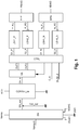
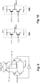
- the scheme of the figure 1 represents the polarization circuit according to the invention which is associated for example with a non-SRAM memory shown in the figure and comprising a matrix of binary storage elements, each storage element comprising at least two inverters, and each inverter comprising a PMOS transistor in series with an NMOS transistor.
- the bias circuit comprises a detection network SN comprising multiple inverters in parallel; these inverters are identical to those of the SRAM memory; they behave like those in memory with respect to their response to changes in polarization voltages.
- This detection network provides at its output SN_out a voltage value Vsn_out which represents the difference between the respective resistances of the NMOS and PMOS transistors in the inverters, that is to say the difference between the capacitances of these transistors to draw current. when their gate receives an intermediate voltage between a blocking voltage and a conduction voltage.
- this network gives an indication of the average force difference between the PMOS and NMOS transistors; for statistical reasons, this average difference represents that of the inverters of the memory to which this detection network is associated.
- This difference in average force depends on the rear biasing voltages applied to the boxes in which the transistors are built, because these rear biasing voltages act directly on the threshold voltages of the transistors.
- the rear biasing voltages NBIAS and PBIAS which are applied to the transistors of the inverters of the memory are also applied to the inverters of the detection network SN so that the detection network faithfully represents the behavior of the inverters of the memory.
- the inverters of the detection network are powered by the same general supply voltage Varray which supplies the memory points of the SRAM memory.
- the power supply is between a voltage Varray and a ground GND referenced to 0 volts.
- the voltage Varray is the reduced supply voltage (compared to the power supply voltage in the mode of normal operation) applied to the network of memory points, allowing a minimization of the consumption while ensuring a permanence of the stored information.
- the polarization circuit according to the invention will make it possible to act on the NBIAS and PBIAS rear biasing voltages of the memory in order both to minimize consumption and to guarantee a sufficient stability of the stored information.
- the inverters conventionally consist of an NMOS transistor having its source at ground, in series with a PMOS transistor having its source at Varray.
- the gates of the two transistors are combined and constitute the input of the inverter; the drains are joined and constitute the exit.
- the PMOS transistor is formed in an N-type well to which a backward bias voltage PBIAS is applied; the NMOS transistor is formed in another P type box to which a NBIAS back bias voltage is applied.
- a common voltage is applied between 0 and Varray, which will be used to evaluate the respective forces of the NMOS transistors. and PMOS.
- this reference voltage is Varray / 2. Inverters receiving on their gates this intermediate voltage tend to switch in one direction or the other depending on the respective strength of the NMOS transistor and the PMOS transistor.
- Vsn_out takes a lower value (and even close to 0) if the NMOS transistors are on average stronger; Vsn_out takes a stronger value (and even close to Varray) if the PMOS transistors are on average stronger. Even if the values of Vsn_out are not exactly 0 and Varray, Vsn_out will be considered as a low or high logic signal depending on whether Vsn_out is greater or less than Varray / 2.
- the output of the detection network SN is preferably applied to a level translator circuit CONVsn_sa which converts the level of the voltage Vsn_out, which is in the voltage range from 0 to Varray, into a logic level in a range of 0 to VDD, where VDD is the general power supply voltage of the integrated circuit.
- This translator circuit has the role of providing an output logic signal SA_in which is equal to zero or equal to VDD depending on whether the NMOS transistors are on average higher or lower than the PMOS transistors.
- CONVsn_sa which can be constituted by a simple threshold comparator whose threshold would be set between 0 and Varray (preferably Varray / 2), or which can even be deleted if the comparison with this threshold is performed. directly into the amplifier stage that follows.
- the output SA_in of this level translator circuit is connected to a sense amplifier SA, the function of which is to compare the value of the signal SA_in with a reference voltage VDD / 2 at the time of a periodic activation signal SA_clk of the following way: the amplifier SA has two outputs OUT1 and OUT2; for an idle state of the activation signal SA_clk the two outputs are pre-loaded to the same level; for an active state of the activation signal, only one of the outputs will go to zero, depending on the level of the input signal SA_in.
- the reference voltage of the SA amplifier is Varray / 2 rather than VDD / 2.
- the activation pulses SA_clk are very short, and therefore the pulses on the output OUT1 or OUT2 are very short. Their brevity makes it possible, as we will see, to periodically adjust the polarization voltages PBIAS and NBIAS by any small increments or decrements in order to guarantee the stability of the polarization.
- the pulses are at least ten times shorter than the period at which they are emitted.
- the sense amplifier therefore provides, at each cycle at the time of the clock CLK, a pulse on the output OUT1 or on the output OUT2, depending on the result of the comparison.
- a pulse on the output OUT1 will cause the incrementation of the NBIAS and PBIAS voltages.
- a pulse on the output OUT2 will cause the decrementation of these voltages.
- the outputs OUT1 and OUT2 of the amplifier SA are applied to a control circuit CTRL which also receives an authorization signal ENABLE and a clock signal CLK.
- the control circuit has two functions: first it establishes the activation signal SA_clk periodically with a period given by the clock CLK; then it establishes four logic signals S1_P, S1_N, S2_P, S2_N to level translator circuits; the two logic signals S1_P and S1_N correspond to the logic level OUT1 but are slightly delayed with respect to OUT1; these are short pulses, emitted if the sense amplifier SA has provided a pulse on OUT1.
- the two logic signals S2_P and S2_N correspond to the logical level OUT2 but are slightly delayed with respect to OUT2; they are brief pulses only if the sense amplifier has provided a pulse on OUT2. It will be seen later that the signals S1_N and S2_P can be inhibited if there is no presence of authorization by an ENABLE signal.
- the signal ENABLE is provided for example at the same time as an order to go into standby mode of the integrated circuit.
- the pulses S1_P will be used to increment the bias voltage PBIAS and at the same time the S1_N pulses will be used to increment the NBIAS polarization.
- the pulses S2_P will be used to decrement the polarization PBIAS and at the same time the S2_N pulses will be used to decrement the NBIAS polarization.
- the logic signals S1_P, S1_N, S2_P, S2_N at the output of the control circuit are in the range 0 to VDD. They are transmitted respectively to each of four level translator circuits LSH1_P, LSH1_N, LSH2_P, LSH2_N which have the following functions: they shift the output level of the signals S1_P, S1_N, S2_P, S2_N from the range 0-VDD to ranges of voltage assigned to the rear biasing voltages PBIAS and NBIAS.
- the bias voltage PBIAS must be able to vary between Varray and Varray +0.9 volts and the bias voltage NBIAS must be able to vary between 0 and -0.9 volts.
- Varray is equal to 0.2 volts, it can be envisaged that PBIAS varies between 0.9 volts and 1.1 volts.
- the level translators LSH1_P and LSH2_P provide incremental pulse logic signals P_PU and decrementation P_PD for the production of the voltage PBIAS; similarly, the level translators LSH1_N and LSH2_N provide logical signals N_PU and N_PD pulses of incrementation and decrementation for the production of NBIAS voltage.
- the signals P_PU and P_PD vary between a voltage Vlow_P and a voltage Vhigh_P, which are for example respectively Varray and Varray + 0,9volt.
- the signals N_PU and N_PD vary between a voltage Vlow_N and a voltage Vhigh_N which are for example respectively -0.9 volts and 0 volts.
- pulsed logical signals thus translated are applied to output circuits BFP and BFN which provide the bias voltages PBIAS and NBIAS.
- These output circuits are integrator circuits which integrate the small incrementation or decrementation variations imposed by the pulses applied to them.
- the pulses P_PU act to increment the voltage PBIAS
- the pulses P_PD act to decrement it.
- the signals N_PU and N_PD act one to increment, the other to decrement, the voltage NBIAS.
- the increments and decrements are small to ensure stability to bias voltages.
- a slaving of the PBIAS and NBIAS voltages thus occurs: a progressive variation of the bias voltages following the pulses in one direction will progressively increase the threshold voltage of one of the NMOS or PMOS transistors of the pair constituting an inverter and decrease that of the other.
- the signal Vsn_out will eventually switch to another logical state than the one he had before.
- This modification will reverse the pulse control signals: if the pulses came from the output OUT1, they will now go to the output OUT2 where they act in the opposite direction (decrement instead of incrementing or the opposite).
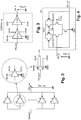
- the figure 2 represents the principle of the detector network SN: it comprises many inverters in parallel, with all their inputs combined into a common input and all their outputs combined into a common output SN_out.
- the inverters are all identical, and identical to the inverters of the SRAM memory that the bias circuit is intended to polarize.
- the inverters of the detection network are all polarized by the polarization circuit itself of which this network is a part; they are polarized in the same way as the other inverters of the integrated circuit.
- the polarization comprises the application of four potentials: the reference potential 0 of the ground GND (the reference 0 is an arbitrary reference) applied to the sources of the NMOS transistors, the potential Varray applied to the sources of the PMOS transistors, the bias voltage NBIAS applied to the P-type wells above or in which the NMOS transistors are formed, and the PBIAS voltage applied to the N-type wells above or in which the PMOS transistors are formed. It is recalled that these bias voltages affect the threshold voltages of the transistors. They therefore affect the respective conductances of the NMOS transistor and the PMOS transistor in an inverter, thus the risk of inadvertent switchover of the inverter when placing the integrated circuit in standby mode with reduced voltage Varray supply.
- the invention is applicable either to technologies in which the transistors are formed directly in boxes P-type (NMOS transistors) or N (PMOS transistors) scattered diffusers, or technologies in which the transistors are each formed above an individual box but separated from this box by other layers. In all cases, the important thing is that the bias voltage of the box influences the threshold voltage of the transistor.
- the number of inverters of the detection network is dictated by statistical considerations: it must be sufficient to correctly represent the average behavior of the inverters of the integrated circuit to be polarized. A number of one hundred will usually be sufficient. In an SRAM memory of several hundred rows and columns, it is possible to use, for example, to form the detection network, the inverters of a fictitious column (in English "dummy column") memory points, these inverters are therefore identical to inverters true memory points but connected differently.
- the figure 3 represents the level translator circuit CONVsn_sa which is recalled that it is optional. It converts the voltage range from 0 to Varray from the SN array into a range of 0 to VDD, where VDD is the general power supply voltage of the integrated circuit.
- first invertor INV1 polarized like the others by the rear biasing voltages PBIAS and NBIAS, and powered between 0 and Varray.
- This inverter receives the voltage Vsn_out; it is preferably constituted by larger transistors than the very small transistors of the SRAM memory. In this way they are less sensitive to the manufacturing dispersions conventionally experienced by small transistors.
- the geometry in terms of ratio W width to length L of the transistor is however the same as that of the transistors of the inverters of the memory.
- the voltage is simply 0 or somehow Varray even if the voltage Vsn_out has a value that is not exactly one of these two values.
- the output of the inverter INV1 is connected to the input of a second inverter INV2 which is supplied between 0 and VDD and whose NMOS transistor is intrinsically much stronger than the PMOS transistor independently of the applied rear biasing voltages: the transistor NMOS has a strong W / L ratio, and the PMOS transistor a weak W / L ratio.
- the goal is to have an inverter switchover point for an input voltage lower than Varray, so that the output of this inverter represents well, but now in the range of 0-VDD voltages, the state of the input of the first inverter.
- the figure 4 represents an embodiment of the sense amplifier SA, supplied between 0 and VDD. Its input SA_in receives the output voltage Vsa_in from the circuit of the figure 3 . It also receives a reference voltage Vref and a periodic activation input SA_clk, and it has two outputs OUT1 and OUT2.
- the reference voltage is preferably VDD / 2; however, if the floor of the figure 3 was absent, this reference voltage would be then Varray / 2 (the amplifier is then powered between 0 and Varray).
- the amplifier compares the input Vsa_in with the reference voltage Vref at times determined by the periodic activation signal SA_clk.
- the activation signal SA_clk is a periodic signal which itself depends on the outputs of the amplifier; it is constituted by a very brief periodic pulse during which the comparison is made.
- the outputs OUT1 and OUT2 are both at the same level, here a high level VDD.
- the outputs are identical when the clock is low and complementary when it is high.
- the output OUT1 goes low when the voltage Vsa_in is greater than Vref, therefore when the output voltage Vsn_out of the detection network is close to Varray; conversely, OUT2 goes low when Vsn_out is close to zero.
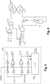
- the figure 5 represents the control circuit CTRL. This circuit receives a periodic clock signal CLK, an authorization signal ENABLE, and the logic signals of the outputs OUT1 and OUT2 of the detection amplifier.
- the signal ENABLE can come for example from a standby order.
- the control circuit comprises logic gates which process the signals OUT1 and OUT2 in a manner to be indicated, and a clock transition detection circuit CEDC which produces the pulse activation signal SA_clk from the signal d periodic clock CLK and from signals OUT1 and OUT2.
- the ENABLE signal is active at low level. It allows outputs S1_N and S2_P respectively to supply the logical values present on OUT1 and OUT2. At the high level, the signal ENABLE forces the signals S1_N and S2_P to zero, the consequence being that the bias circuit no longer performs its regulation function of NBIAS and PBIAS but forces NBIAS and PBIAS to nominal values which are preferably zero. for NBIAS and Varray for PBIAS.
- the zero crossing pulses of OUT1 are transferred to the outputs S1_N and S1_P; the OUT2 pulses are reported on the outputs S2_N and S2_P.
- the signals on the outputs S1_N and S2_N serve as a control for the detection circuit of clock transitions CEDC.
- This circuit periodically produces a very short pulse SA_clk during which the comparison is carried out in the detection amplifier.
- the circuit CEDC receives for this purpose the periodic clock CLK whose high and low slots are of identical duration. It also receives the ENABLE signal and here again we consider the case where ENABLE is active (standby mode), therefore at the low level. If ENABLE was inactive (high level) the circuit would not produce SA_clk pulses.
- the clock transition detection circuit is represented at the figure 6 .
- An AND gate 10 transmits the clock CLK and its delayed complement by one or more inverters in series to the inputs of another AND gate 12 so as to produce a short trigger pulse on the rising edge of the clock signal; this pulse, applied to a first input of a RS flip-flop (consisting of two NI gates 14 and 16 looped one over the other), switches the flip-flop, causing the output signal SA_clk to go high, initially at low level.
- the comparison process is then done in the sense amplifier during this brief pulse.
- One of the signals OUT1 or OUT2 will therefore go to zero during this pulse.
- the signals S1_N and S2_N (corresponding to signals OUT1 and OUT2 but slightly delayed) are applied to the inputs of an exclusive-OR gate 18 which supplies a logic signal in general which is zero when S1_N and S2_N are both at level 1 and which provides a logic signal high when either of OUT1 and OUT2 goes to zero.
- the passage to the high level of the output of the gate 18 makes again switch the flip-flop 14, 16 which reduces to zero the SA_clk signal, interrupting the activation signal which is very brief.
- the signal OUT1 or OUT2 which has passed to the low level returns to the high level imposed by the interruption of the activation signal; the signals S1_N, S1_P, S2_N, S2_P all return to the high level again.
- An OR gate 20 receives the ENABLE signal to block the flip-flop with SA_clk at the low level when ENABLE is at the inactive level (high level) to prohibit the servocontrol of the bias voltages.
- the pulse serves, in the manner of a charge pump, to increment or decrement the average voltage PBIAS or NBIAS by injecting a short charge or discharge current for the duration of the pulse. It is the overall natural capacity of the regions polarized by the PBIAS and NBIAS voltages that keeps the bias voltage at a mean value between two pulses.
- the signals S1_N, S1_P, S2_N, S2_P are between 0 (low level) and VDD (high level). They must be brought back to a voltage range corresponding to the voltage range in which the NBIAS and PBIAS voltages can evolve.
- the voltage Varray is 0.2 volts and it is desired that the rear biasing voltages can vary between 0 volts and -0.9 volts for NBIAS and between 0.2 volts and 1.1 volts for PBIAS.
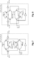
- the figure 7 represents the configuration of a LSH1_P level translator which can be used for translation to higher potentials. It receives the pulse S1_P and provides a pulse P_PU on one of its outputs; the pulse P_PU is an incrementation pulse of the voltage PBIAS and it must be, as will be seen, a pulse of passage to the low logical level because it controls a PMOS transistor.
- the circuit LSH1_P has a second output referenced P_PD, logical complement of the first, but which is not used.
- the level translator LSH2_P is strictly identical but it receives the pulse S2_P and it uses the second output P_PD and not the first; in fact, it must produce a pulse of decrementation of the voltage PBIAS and this pulse must be a pulse of passage to the logic high level because it controls an NMOS transistor.
- Vhigh_P and Vlow_P have been called voltage sources for transposing the pulse levels to the voltage range from Vlow_P to Vhigh_P.
- the zero reference potential is used in this scheme.
- Vlow_P is in principle equal to Varray;
- Vhigh_P can be equal to Varray + 0.9 volts.
- figure 8 represents a level translator LSH1_N for a translation to lower potentials. It receives the pulse S1_N and provides an N_PU pulse on one of its outputs (low-pass pulse for the control of a PMOS transistor incrementation of NBIAS); it has a complementary logical output N_PD which is not used.
- the translator LSH2_N is identical, it receives the pulse S2_N and it provides a pulse on the second output N_PD and not the first (high-pass pulse for the control of a NMOS transistor decrementation of NBIAS).
- Vhigh_N is in principle equal to 0; Vlow_N can be equal to -0.9 volts.
- the figure 9 is another example of a level translator circuit that can be used for both upward and downward level translation.
- figure 10 represents the two integrator stages of output BFP and BFN supplying the voltages PBIAS and NBIAS. These are stages each comprising an NMOS transistor in series with a PMOS transistor. These series assemblies are powered by the potentials Vhigh_P and Vlow_P for the stage supplying the potential PBIAS ( figure 10A ) or by the potentials Vhigh_N and Vlow_N for the stage supplying the potential NBIAS ( figure 10B ).
- the pulses of the P_PU and P_PD outputs of the level translators are respectively applied to the gate of the PMOS transistor and to the gate of the NMOS transistor for the stage which supplies the bias voltage PBIAS.
- the logic levels N_PU and N_PD are applied to the gates of the transistors of the stage which supplies the bias voltage PBIAS.
- the pulse P_PU (incrementation of PBIAS) is a zero crossing pulse (Vlow_P) and briefly turns on the PMOS transistor.
- the pulse P_PD (decrementation of PBIAS) is a high-pass pulse (Vhigh_P) and briefly turns on the NMOS transistor.
- the pulse N_PU (incrementation of NBIAS) is a high-pass pulse (Vhigh_N) and briefly turns on the PMOS transistor.
- the pulse N_PD (decrementation of NBIAS) is a low-pass pulse (Vlow_N) and briefly turns on the NMOS transistor.
Landscapes
- Engineering & Computer Science (AREA)
- Microelectronics & Electronic Packaging (AREA)
- Computer Hardware Design (AREA)
- Power Engineering (AREA)
- Logic Circuits (AREA)
Claims (11)
- Invertervorspannungsschaltung einer integrierten Schaltung, wobei jeder Inverter einen NMOS-Transistor und einen PMOS-Transistor umfasst, die mit einer Speisespannung Varray gespeist werden, mit Mitteln zum Anlegen einer ersten Rückwärtsvorspannung (NBAS) an die NMOS-Transistoren und einer zweiten Rückwärtsvorspannung (PBIAS) an die PMOS-Transistoren, wobei die erfindungsgemäße Vorspannungsschaltung diese Vorspannungen liefert und Folgendes umfasst:- ein Erkennungsnetz (SN), das mehrere parallel geschaltete Inverter umfasst, wobei die Inverter von der Speisespannung Varray gespeist und mit den beiden Rückwärtsvorspannungen vorgespannt werden und an ihrem Gate eine selbe Referenzspannung zwischen 0 und der Speisespannung Varray der Inverter empfangen, wobei der gemeinsame Ausgang der Inverter den Ausgang (SN_out) des Erkennungsnetzes bildet, wobei dieser Ausgang ein Logiksignal liefert, dessen Wert von von den an das Netzwerk angelegten Rückwärtsvorspannungen abhängig ist,- eine Inkrementier- oder Dekrementierimpulserzeugungsschaltung (CTRL, SA), gesteuert durch den Ausgang des Erkennungsnetzes,- und eine Integrationsschaltung (BSP, BSN), verbunden mit der Impulserzeugungsschaltung, zum Erzeugen und progressiven inkrementalen Variieren, als Reaktion auf diese Impulse, der ersten Rückwärtsvorspannung (NBIAS) und der zweiten Rückwärtsvorspannung (PBIAS) in einer Richtung, die dazu neigt, das Ausgangslogiksignal des Erkennungsnetzes umzukehren.
- Vorspannungsschaltung nach Anspruch 1, dadurch gekennzeichnet, dass die an die Gates der Transistoren der Inverter des Erkennungsnetzes angelegte Referenzspannung Varray/2 ist.
- Vorspannungsschaltung nach einem der Ansprüche 1 und 2, dadurch gekennzeichnet, dass eine Logikpegelumsetzschaltung (CONVsn_sa) zwischen den Ausgang des Erkennungsnetzes und den Eingang der Impulserzeugungsschaltung geschaltet ist.
- Vorspannungsschaltung nach einem der Ansprüche 1 bis 3, dadurch gekennzeichnet, dass die Impulserzeugungsschaltung einen Erkennungsverstärker (SA) und eine Steuerschaltung (CTRL) umfasst, wobei die Steuerschaltung eine Taktschaltung (CEDC) umfasst, die periodisch ein Aktivierungssignal erzeugt, das von kurzen Impulsen gebildet wird, die Aktivierungsimpulse des Erkennungsverstärkers sind, wobei der Erkennungsverstärker eine vom Erkennungsnetz kommende Spannung empfängt und als Komparator mit Bezug auf eine Referenzspannung agiert, um an einem von zwei Ausgängen (OUT1, OUT2) einen Steuerimpuls in Abhängigkeit vom Ergebnis des Vergleichs zu erzeugen.
- Vorspannungsschaltung nach Anspruch 4, dadurch gekennzeichnet, dass die Steuerspannung die beiden Ausgänge des Erkennungsverstärkers empfängt und vier entsprechende Impulslogiksignale erzeugt, in Abhängigkeit von den Ergebnissen des Vergleichs, jeweils gesendet zu vier Pegelumsetzschaltungen, wobei zwei erste Pegelumsetzschaltungen zwei der Signale in einen Spannungsbereich entsprechend einem gewünschten Spannungsvariationsbereich für die zweite Rückwärtsvorspannung (PBIAS) umwandelt, und wobei zwei andere Pegelumsetzschaltungen die beiden anderen Signale in einen Spannungsbereich entsprechend einem gewünschten Spannungsvariationsbereich für die erste Rückwärtsvorspannung (NBIAS) umwandeln.
- Vorspannungsschaltung nach Anspruch 5, dadurch gekennzeichnet, dass die Integrationsschaltung (BFP, BSN) eine erste Schaltung zum Erzeugen der zweiten Rückwärtsvorspannung (PBIAS) und eine zweite Schaltung zum Erzeugen der ersten Rückwärtsvorspannung (NBIAS) umfasst, wobei die erste Schaltung an ihren Eingängen die Ausgänge von zwei ersten Pegelumsetzschaltungen empfängt und die zweite Schaltung an ihren Eingängen die Ausgänge der beiden anderen Pegelumsetzschaltungen empfängt.
- Vorspannungsschaltung nach Anspruch 6, dadurch gekennzeichnet, dass die erste und die zweite Schaltung jeweils einen PMOS-Transistor in Serie mit einem NMOS-Transistor umfassen, die die zweite Vorspannung (PPIAS) bzw. die erste Vorspannung (NBIAS) am Übergangspunkt dieser beiden Transistoren liefern, wobei die Ausgänge der Pegelumsetzschaltungen an die Gates dieser Transistoren angelegt werden, wobei alle Transistoren in Serie von der ersten Schaltung mit einer Spannung zwischen einer tiefen Spannung (Vlow_P) und einer hohen Spannung (Vhigh_P) entsprechend dem gewünschten Spannungsbereich für die Variation der zweiten Vorspannung (PBIAS) gespeist werden und wobei alle Transistoren in Serie von der zweiten Schaltung mit einer Spannung zwischen einer tiefen Spannung (Vlow_N) und einer hohen Spannung (Vhigh_N) entsprechend dem gewünschten Spannungsbereich für die Variation der ersten Vorspannung (NBIAS) gespeist werden.
- Vorspannungsschaltung nach einem der Ansprüche 1 bis 7, dadurch gekennzeichnet, dass sie die zweite und erste Rückwärtsvorspannung (PBIAS, NBIAS) an die PMOS- und NMOS-Transistoren der Inverter eines SRAM anlegt.
- Vorspannungsschaltung nach Anspruch 8, dadurch gekennzeichnet, dass sie einen Autorisierungseingang (ENABLE) umfasst, der das Anlegen von Inkrementier- oder Dekrementierimpulsen an die Integrationsschaltung zulässt oder nicht zulässt, insbesondere zum Autorisieren dieses Anlegens im Standby-Modus mit reduzierter Spannungsspeisung des Speichers.
- Vorspannungsschaltung nach einem der Ansprüche 1 bis 9, dadurch gekennzeichnet, dass sie Mittel zum Anlegen der mit Bezug auf eine allgemeine Speisespannung (VDD) der integrierten Schaltung reduzierten Speisespannung Varray an die Inverter im Standby-Modus umfasst.
- Integrierte Schaltung, die einen SRAM umfasst, gebildet von einer Matrix von binären Speicherelementen und einer Vorspannungsschaltung nach einem der Ansprüche 1 bis 10, dadurch gekennzeichnet, dass jedes Speicherelement wenigstens zwei mit den Invertern des Erkennungsnetzes identische Inverter umfasst.
Applications Claiming Priority (2)
| Application Number | Priority Date | Filing Date | Title |
|---|---|---|---|
| FR1160085A FR2982417B1 (fr) | 2011-11-07 | 2011-11-07 | Circuit de polarisation arriere pour reduction de la consommation d'un circuit integre |
| PCT/EP2012/070666 WO2013068221A1 (fr) | 2011-11-07 | 2012-10-18 | Circuit de polarisation arriere d'inverseurs pour reduction de la consommation d'une mémoire sram |
Publications (2)
| Publication Number | Publication Date |
|---|---|
| EP2777045A1 EP2777045A1 (de) | 2014-09-17 |
| EP2777045B1 true EP2777045B1 (de) | 2017-09-06 |
Family
ID=47046609
Family Applications (1)
| Application Number | Title | Priority Date | Filing Date |
|---|---|---|---|
| EP12775242.6A Not-in-force EP2777045B1 (de) | 2011-11-07 | 2012-10-18 | Schaltungsanordnung zur vorspannung der invertern-wannen zur reduzierung des energieverbrauchs eines srams |
Country Status (4)
| Country | Link |
|---|---|
| US (1) | US9099993B2 (de) |
| EP (1) | EP2777045B1 (de) |
| FR (1) | FR2982417B1 (de) |
| WO (1) | WO2013068221A1 (de) |
Families Citing this family (1)
| Publication number | Priority date | Publication date | Assignee | Title |
|---|---|---|---|---|
| TWI685842B (zh) * | 2017-12-13 | 2020-02-21 | 湯朝景 | 3t1d sram細胞以及用於靜態隨機存取記憶體的存取方法及相關的裝置 |
Family Cites Families (3)
| Publication number | Priority date | Publication date | Assignee | Title |
|---|---|---|---|---|
| JP3614546B2 (ja) * | 1995-12-27 | 2005-01-26 | 富士通株式会社 | 半導体集積回路 |
| JP4090231B2 (ja) * | 2001-11-01 | 2008-05-28 | 株式会社ルネサステクノロジ | 半導体集積回路装置 |
| KR100610020B1 (ko) * | 2005-01-13 | 2006-08-08 | 삼성전자주식회사 | 반도체 메모리 장치에서의 셀 파워 스위칭 회로와 그에따른 셀 파워 전압 인가방법 |
-
2011
- 2011-11-07 FR FR1160085A patent/FR2982417B1/fr active Active
-
2012
- 2012-10-18 US US14/356,562 patent/US9099993B2/en not_active Expired - Fee Related
- 2012-10-18 WO PCT/EP2012/070666 patent/WO2013068221A1/fr not_active Ceased
- 2012-10-18 EP EP12775242.6A patent/EP2777045B1/de not_active Not-in-force
Non-Patent Citations (1)
| Title |
|---|
| None * |
Also Published As
| Publication number | Publication date |
|---|---|
| FR2982417B1 (fr) | 2014-05-16 |
| FR2982417A1 (fr) | 2013-05-10 |
| US20140334226A1 (en) | 2014-11-13 |
| EP2777045A1 (de) | 2014-09-17 |
| WO2013068221A1 (fr) | 2013-05-16 |
| US9099993B2 (en) | 2015-08-04 |
Similar Documents
| Publication | Publication Date | Title |
|---|---|---|
| EP1863179B1 (de) | Niveauverschiebungsschaltkreis | |
| EP0080394B1 (de) | Bistabile Kippschaltung mit energieunabhängiger Haltbarkeit und statischer Rücksetzung | |
| EP2047475A2 (de) | Schaltung zur auslesung eines ladungszurückhaltungselements zur zeitmessung | |
| FR2988535A1 (fr) | Circuit de pompage de charge a transistors munis de portes doubles en phase, et procédé de fonctionnement dudit circuit. | |
| EP3002788B1 (de) | Vorrichtung mit sram-speicherzellen die mitteln zur polarisierung der wannen der speicherzelltransistoren umfasst | |
| FR2762434A1 (fr) | Circuit de lecture de memoire avec dispositif de limitation de precharge | |
| EP0262013B1 (de) | Leseverstärker | |
| EP2073212B1 (de) | Lesevorrichtung eines nichtflüchtigen Speichers mit geringem Energieverbrauch und ihr Anwendungsverfahren | |
| FR2822309A1 (fr) | Circuit de translation de signaux de commutation | |
| EP1073203B1 (de) | Steuerschaltung für einen Pegelumsetzer-Hochspannungsschalter | |
| EP2777045B1 (de) | Schaltungsanordnung zur vorspannung der invertern-wannen zur reduzierung des energieverbrauchs eines srams | |
| EP1727147B1 (de) | Leseverstärker für einen dynamischen Speicher | |
| EP1818942B1 (de) | Nichtflüchtige Speichervorrichtung | |
| EP3079260A1 (de) | Verfahren und vorrichtung zur automatischen kalibrierung von multi-grid-schaltkreisen | |
| FR2768274A1 (fr) | Circuit de generation d'une haute tension de programmation ou d'effacement d'une memoire | |
| FR2750240A1 (fr) | Generateur de reference de tension | |
| EP2087592B1 (de) | Vor batterieverpolung geschützte logikausgangsstufe einer integrierten schaltung | |
| EP0678868A1 (de) | Spannungsvervielfacherschaltung | |
| FR2879375A1 (fr) | Dispositif de reinitialisation d'un circuit integre a partir d'une detection d'une chute d'une tension d'alimentation, et circuit electronique correspondant | |
| EP3182617B1 (de) | Optischer empfänger mit relativer phasendetektion | |
| EP0897182A1 (de) | Strahlungsunempfindliche statische Speicherzelle | |
| FR2967522A1 (fr) | Memoire non-volatile securisee | |
| FR2905043A1 (fr) | Circuit bistable a basculement d'etat auto-ajuste temporellement et bascule flip-flop utilisant un tel circuit bistable. | |
| EP1398793B1 (de) | MOS technologische digital integrierte Schaltung | |
| FR3055735A1 (fr) | Amplificateur de detection apte a controler une operation de lecture dans une memoire |
Legal Events
| Date | Code | Title | Description |
|---|---|---|---|
| PUAI | Public reference made under article 153(3) epc to a published international application that has entered the european phase |
Free format text: ORIGINAL CODE: 0009012 |
|
| 17P | Request for examination filed |
Effective date: 20140429 |
|
| AK | Designated contracting states |
Kind code of ref document: A1 Designated state(s): AL AT BE BG CH CY CZ DE DK EE ES FI FR GB GR HR HU IE IS IT LI LT LU LV MC MK MT NL NO PL PT RO RS SE SI SK SM TR |
|
| DAX | Request for extension of the european patent (deleted) | ||
| GRAP | Despatch of communication of intention to grant a patent |
Free format text: ORIGINAL CODE: EPIDOSNIGR1 |
|
| RIC1 | Information provided on ipc code assigned before grant |
Ipc: G11C 11/4074 20060101ALI20170126BHEP Ipc: G11C 11/41 20060101ALI20170126BHEP Ipc: G11C 11/417 20060101ALI20170126BHEP Ipc: H03K 3/012 20060101ALI20170126BHEP Ipc: G11C 5/14 20060101AFI20170126BHEP Ipc: G11C 11/412 20060101ALI20170126BHEP Ipc: G11C 13/00 20060101ALN20170126BHEP |
|
| INTG | Intention to grant announced |
Effective date: 20170216 |
|
| GRAJ | Information related to disapproval of communication of intention to grant by the applicant or resumption of examination proceedings by the epo deleted |
Free format text: ORIGINAL CODE: EPIDOSDIGR1 |
|
| RIN1 | Information on inventor provided before grant (corrected) |
Inventor name: THOMAS, OLIVIER Inventor name: VLADIMIRESCU, ANDREI Inventor name: MAKOSIEJ, ADAM |
|
| GRAP | Despatch of communication of intention to grant a patent |
Free format text: ORIGINAL CODE: EPIDOSNIGR1 |
|
| INTC | Intention to grant announced (deleted) | ||
| RIC1 | Information provided on ipc code assigned before grant |
Ipc: G11C 13/00 20060101ALN20170323BHEP Ipc: G11C 11/41 20060101ALI20170323BHEP Ipc: G11C 11/417 20060101ALI20170323BHEP Ipc: G11C 5/14 20060101AFI20170323BHEP Ipc: G11C 11/4074 20060101ALI20170323BHEP Ipc: G11C 11/412 20060101ALI20170323BHEP Ipc: H03K 3/012 20060101ALI20170323BHEP |
|
| INTG | Intention to grant announced |
Effective date: 20170410 |
|
| GRAS | Grant fee paid |
Free format text: ORIGINAL CODE: EPIDOSNIGR3 |
|
| GRAA | (expected) grant |
Free format text: ORIGINAL CODE: 0009210 |
|
| AK | Designated contracting states |
Kind code of ref document: B1 Designated state(s): AL AT BE BG CH CY CZ DE DK EE ES FI FR GB GR HR HU IE IS IT LI LT LU LV MC MK MT NL NO PL PT RO RS SE SI SK SM TR |
|
| REG | Reference to a national code |
Ref country code: GB Ref legal event code: FG4D Free format text: NOT ENGLISH |
|
| REG | Reference to a national code |
Ref country code: CH Ref legal event code: EP Ref country code: AT Ref legal event code: REF Ref document number: 926671 Country of ref document: AT Kind code of ref document: T Effective date: 20170915 |
|
| REG | Reference to a national code |
Ref country code: FR Ref legal event code: PLFP Year of fee payment: 6 |
|
| REG | Reference to a national code |
Ref country code: IE Ref legal event code: FG4D Free format text: LANGUAGE OF EP DOCUMENT: FRENCH |
|
| REG | Reference to a national code |
Ref country code: DE Ref legal event code: R096 Ref document number: 602012037003 Country of ref document: DE |
|
| REG | Reference to a national code |
Ref country code: NL Ref legal event code: MP Effective date: 20170906 |
|
| REG | Reference to a national code |
Ref country code: LT Ref legal event code: MG4D |
|
| PG25 | Lapsed in a contracting state [announced via postgrant information from national office to epo] |
Ref country code: SE Free format text: LAPSE BECAUSE OF FAILURE TO SUBMIT A TRANSLATION OF THE DESCRIPTION OR TO PAY THE FEE WITHIN THE PRESCRIBED TIME-LIMIT Effective date: 20170906 Ref country code: LT Free format text: LAPSE BECAUSE OF FAILURE TO SUBMIT A TRANSLATION OF THE DESCRIPTION OR TO PAY THE FEE WITHIN THE PRESCRIBED TIME-LIMIT Effective date: 20170906 Ref country code: NO Free format text: LAPSE BECAUSE OF FAILURE TO SUBMIT A TRANSLATION OF THE DESCRIPTION OR TO PAY THE FEE WITHIN THE PRESCRIBED TIME-LIMIT Effective date: 20171206 Ref country code: FI Free format text: LAPSE BECAUSE OF FAILURE TO SUBMIT A TRANSLATION OF THE DESCRIPTION OR TO PAY THE FEE WITHIN THE PRESCRIBED TIME-LIMIT Effective date: 20170906 Ref country code: HR Free format text: LAPSE BECAUSE OF FAILURE TO SUBMIT A TRANSLATION OF THE DESCRIPTION OR TO PAY THE FEE WITHIN THE PRESCRIBED TIME-LIMIT Effective date: 20170906 |
|
| REG | Reference to a national code |
Ref country code: AT Ref legal event code: MK05 Ref document number: 926671 Country of ref document: AT Kind code of ref document: T Effective date: 20170906 |
|
| PG25 | Lapsed in a contracting state [announced via postgrant information from national office to epo] |
Ref country code: RS Free format text: LAPSE BECAUSE OF FAILURE TO SUBMIT A TRANSLATION OF THE DESCRIPTION OR TO PAY THE FEE WITHIN THE PRESCRIBED TIME-LIMIT Effective date: 20170906 Ref country code: ES Free format text: LAPSE BECAUSE OF FAILURE TO SUBMIT A TRANSLATION OF THE DESCRIPTION OR TO PAY THE FEE WITHIN THE PRESCRIBED TIME-LIMIT Effective date: 20170906 Ref country code: LV Free format text: LAPSE BECAUSE OF FAILURE TO SUBMIT A TRANSLATION OF THE DESCRIPTION OR TO PAY THE FEE WITHIN THE PRESCRIBED TIME-LIMIT Effective date: 20170906 Ref country code: GR Free format text: LAPSE BECAUSE OF FAILURE TO SUBMIT A TRANSLATION OF THE DESCRIPTION OR TO PAY THE FEE WITHIN THE PRESCRIBED TIME-LIMIT Effective date: 20171207 Ref country code: BG Free format text: LAPSE BECAUSE OF FAILURE TO SUBMIT A TRANSLATION OF THE DESCRIPTION OR TO PAY THE FEE WITHIN THE PRESCRIBED TIME-LIMIT Effective date: 20171206 |
|
| PG25 | Lapsed in a contracting state [announced via postgrant information from national office to epo] |
Ref country code: NL Free format text: LAPSE BECAUSE OF FAILURE TO SUBMIT A TRANSLATION OF THE DESCRIPTION OR TO PAY THE FEE WITHIN THE PRESCRIBED TIME-LIMIT Effective date: 20170906 |
|
| PG25 | Lapsed in a contracting state [announced via postgrant information from national office to epo] |
Ref country code: RO Free format text: LAPSE BECAUSE OF FAILURE TO SUBMIT A TRANSLATION OF THE DESCRIPTION OR TO PAY THE FEE WITHIN THE PRESCRIBED TIME-LIMIT Effective date: 20170906 Ref country code: PL Free format text: LAPSE BECAUSE OF FAILURE TO SUBMIT A TRANSLATION OF THE DESCRIPTION OR TO PAY THE FEE WITHIN THE PRESCRIBED TIME-LIMIT Effective date: 20170906 Ref country code: CZ Free format text: LAPSE BECAUSE OF FAILURE TO SUBMIT A TRANSLATION OF THE DESCRIPTION OR TO PAY THE FEE WITHIN THE PRESCRIBED TIME-LIMIT Effective date: 20170906 |
|
| PG25 | Lapsed in a contracting state [announced via postgrant information from national office to epo] |
Ref country code: IS Free format text: LAPSE BECAUSE OF FAILURE TO SUBMIT A TRANSLATION OF THE DESCRIPTION OR TO PAY THE FEE WITHIN THE PRESCRIBED TIME-LIMIT Effective date: 20180106 Ref country code: EE Free format text: LAPSE BECAUSE OF FAILURE TO SUBMIT A TRANSLATION OF THE DESCRIPTION OR TO PAY THE FEE WITHIN THE PRESCRIBED TIME-LIMIT Effective date: 20170906 Ref country code: IT Free format text: LAPSE BECAUSE OF FAILURE TO SUBMIT A TRANSLATION OF THE DESCRIPTION OR TO PAY THE FEE WITHIN THE PRESCRIBED TIME-LIMIT Effective date: 20170906 Ref country code: SK Free format text: LAPSE BECAUSE OF FAILURE TO SUBMIT A TRANSLATION OF THE DESCRIPTION OR TO PAY THE FEE WITHIN THE PRESCRIBED TIME-LIMIT Effective date: 20170906 Ref country code: AT Free format text: LAPSE BECAUSE OF FAILURE TO SUBMIT A TRANSLATION OF THE DESCRIPTION OR TO PAY THE FEE WITHIN THE PRESCRIBED TIME-LIMIT Effective date: 20170906 Ref country code: SM Free format text: LAPSE BECAUSE OF FAILURE TO SUBMIT A TRANSLATION OF THE DESCRIPTION OR TO PAY THE FEE WITHIN THE PRESCRIBED TIME-LIMIT Effective date: 20170906 |
|
| REG | Reference to a national code |
Ref country code: CH Ref legal event code: PL |
|
| REG | Reference to a national code |
Ref country code: DE Ref legal event code: R097 Ref document number: 602012037003 Country of ref document: DE |
|
| PG25 | Lapsed in a contracting state [announced via postgrant information from national office to epo] |
Ref country code: MC Free format text: LAPSE BECAUSE OF FAILURE TO SUBMIT A TRANSLATION OF THE DESCRIPTION OR TO PAY THE FEE WITHIN THE PRESCRIBED TIME-LIMIT Effective date: 20170906 |
|
| PLBE | No opposition filed within time limit |
Free format text: ORIGINAL CODE: 0009261 |
|
| STAA | Information on the status of an ep patent application or granted ep patent |
Free format text: STATUS: NO OPPOSITION FILED WITHIN TIME LIMIT |
|
| REG | Reference to a national code |
Ref country code: IE Ref legal event code: MM4A |
|
| PG25 | Lapsed in a contracting state [announced via postgrant information from national office to epo] |
Ref country code: CH Free format text: LAPSE BECAUSE OF NON-PAYMENT OF DUE FEES Effective date: 20171031 Ref country code: LU Free format text: LAPSE BECAUSE OF NON-PAYMENT OF DUE FEES Effective date: 20171018 Ref country code: LI Free format text: LAPSE BECAUSE OF NON-PAYMENT OF DUE FEES Effective date: 20171031 Ref country code: DK Free format text: LAPSE BECAUSE OF FAILURE TO SUBMIT A TRANSLATION OF THE DESCRIPTION OR TO PAY THE FEE WITHIN THE PRESCRIBED TIME-LIMIT Effective date: 20170906 |
|
| 26N | No opposition filed |
Effective date: 20180607 |
|
| REG | Reference to a national code |
Ref country code: BE Ref legal event code: MM Effective date: 20171031 |
|
| GBPC | Gb: european patent ceased through non-payment of renewal fee |
Effective date: 20171206 |
|
| PG25 | Lapsed in a contracting state [announced via postgrant information from national office to epo] |
Ref country code: BE Free format text: LAPSE BECAUSE OF NON-PAYMENT OF DUE FEES Effective date: 20171031 Ref country code: SI Free format text: LAPSE BECAUSE OF FAILURE TO SUBMIT A TRANSLATION OF THE DESCRIPTION OR TO PAY THE FEE WITHIN THE PRESCRIBED TIME-LIMIT Effective date: 20170906 |
|
| PG25 | Lapsed in a contracting state [announced via postgrant information from national office to epo] |
Ref country code: MT Free format text: LAPSE BECAUSE OF FAILURE TO SUBMIT A TRANSLATION OF THE DESCRIPTION OR TO PAY THE FEE WITHIN THE PRESCRIBED TIME-LIMIT Effective date: 20170906 |
|
| REG | Reference to a national code |
Ref country code: FR Ref legal event code: PLFP Year of fee payment: 7 |
|
| PG25 | Lapsed in a contracting state [announced via postgrant information from national office to epo] |
Ref country code: IE Free format text: LAPSE BECAUSE OF NON-PAYMENT OF DUE FEES Effective date: 20171018 |
|
| PG25 | Lapsed in a contracting state [announced via postgrant information from national office to epo] |
Ref country code: GB Free format text: LAPSE BECAUSE OF NON-PAYMENT OF DUE FEES Effective date: 20171206 |
|
| PG25 | Lapsed in a contracting state [announced via postgrant information from national office to epo] |
Ref country code: HU Free format text: LAPSE BECAUSE OF FAILURE TO SUBMIT A TRANSLATION OF THE DESCRIPTION OR TO PAY THE FEE WITHIN THE PRESCRIBED TIME-LIMIT; INVALID AB INITIO Effective date: 20121018 |
|
| PG25 | Lapsed in a contracting state [announced via postgrant information from national office to epo] |
Ref country code: CY Free format text: LAPSE BECAUSE OF NON-PAYMENT OF DUE FEES Effective date: 20170906 |
|
| PG25 | Lapsed in a contracting state [announced via postgrant information from national office to epo] |
Ref country code: MK Free format text: LAPSE BECAUSE OF FAILURE TO SUBMIT A TRANSLATION OF THE DESCRIPTION OR TO PAY THE FEE WITHIN THE PRESCRIBED TIME-LIMIT Effective date: 20170906 |
|
| PG25 | Lapsed in a contracting state [announced via postgrant information from national office to epo] |
Ref country code: TR Free format text: LAPSE BECAUSE OF FAILURE TO SUBMIT A TRANSLATION OF THE DESCRIPTION OR TO PAY THE FEE WITHIN THE PRESCRIBED TIME-LIMIT Effective date: 20170906 |
|
| PG25 | Lapsed in a contracting state [announced via postgrant information from national office to epo] |
Ref country code: PT Free format text: LAPSE BECAUSE OF FAILURE TO SUBMIT A TRANSLATION OF THE DESCRIPTION OR TO PAY THE FEE WITHIN THE PRESCRIBED TIME-LIMIT Effective date: 20170906 |
|
| PG25 | Lapsed in a contracting state [announced via postgrant information from national office to epo] |
Ref country code: AL Free format text: LAPSE BECAUSE OF FAILURE TO SUBMIT A TRANSLATION OF THE DESCRIPTION OR TO PAY THE FEE WITHIN THE PRESCRIBED TIME-LIMIT Effective date: 20170906 |
|
| PGFP | Annual fee paid to national office [announced via postgrant information from national office to epo] |
Ref country code: DE Payment date: 20201009 Year of fee payment: 9 Ref country code: FR Payment date: 20201030 Year of fee payment: 9 |
|
| REG | Reference to a national code |
Ref country code: DE Ref legal event code: R119 Ref document number: 602012037003 Country of ref document: DE |
|
| PG25 | Lapsed in a contracting state [announced via postgrant information from national office to epo] |
Ref country code: DE Free format text: LAPSE BECAUSE OF NON-PAYMENT OF DUE FEES Effective date: 20220503 |
|
| PG25 | Lapsed in a contracting state [announced via postgrant information from national office to epo] |
Ref country code: FR Free format text: LAPSE BECAUSE OF NON-PAYMENT OF DUE FEES Effective date: 20211031 |