EP2777045B1 - Polarisation circuit of inverters wells reducing power consumption of an sram - Google Patents
Polarisation circuit of inverters wells reducing power consumption of an sram Download PDFInfo
- Publication number
- EP2777045B1 EP2777045B1 EP12775242.6A EP12775242A EP2777045B1 EP 2777045 B1 EP2777045 B1 EP 2777045B1 EP 12775242 A EP12775242 A EP 12775242A EP 2777045 B1 EP2777045 B1 EP 2777045B1
- Authority
- EP
- European Patent Office
- Prior art keywords
- voltage
- circuit
- bias
- inverters
- pbias
- Prior art date
- Legal status (The legal status is an assumption and is not a legal conclusion. Google has not performed a legal analysis and makes no representation as to the accuracy of the status listed.)
- Not-in-force
Links
- 238000001514 detection method Methods 0.000 claims description 39
- 230000015654 memory Effects 0.000 claims description 31
- 230000004913 activation Effects 0.000 claims description 22
- 238000013519 translation Methods 0.000 claims description 11
- 230000010354 integration Effects 0.000 claims description 6
- KQDWMXVMXQCPIZ-UHFFFAOYSA-N 4-amino-5-(2-chloroethyl)-1-[4-hydroxy-5-(hydroxymethyl)oxolan-2-yl]pyrimidin-2-one Chemical compound C1=C(CCCl)C(N)=NC(=O)N1C1OC(CO)C(O)C1 KQDWMXVMXQCPIZ-UHFFFAOYSA-N 0.000 claims description 4
- 230000004044 response Effects 0.000 claims description 4
- 239000011159 matrix material Substances 0.000 claims description 2
- 230000010287 polarization Effects 0.000 description 17
- 238000004519 manufacturing process Methods 0.000 description 8
- 230000000737 periodic effect Effects 0.000 description 8
- 230000006399 behavior Effects 0.000 description 6
- 230000006870 function Effects 0.000 description 6
- 230000000295 complement effect Effects 0.000 description 5
- 238000013475 authorization Methods 0.000 description 4
- 230000003111 delayed effect Effects 0.000 description 4
- 101150110971 CIN7 gene Proteins 0.000 description 3
- 101150110298 INV1 gene Proteins 0.000 description 3
- 101100397044 Xenopus laevis invs-a gene Proteins 0.000 description 3
- 238000000034 method Methods 0.000 description 3
- 230000007704 transition Effects 0.000 description 3
- 238000006243 chemical reaction Methods 0.000 description 2
- 238000005516 engineering process Methods 0.000 description 2
- 238000012423 maintenance Methods 0.000 description 2
- 230000004048 modification Effects 0.000 description 2
- 238000012986 modification Methods 0.000 description 2
- 230000008569 process Effects 0.000 description 2
- 230000002441 reversible effect Effects 0.000 description 2
- 101100286980 Daucus carota INV2 gene Proteins 0.000 description 1
- 101100397045 Xenopus laevis invs-b gene Proteins 0.000 description 1
- 230000001133 acceleration Effects 0.000 description 1
- 230000006978 adaptation Effects 0.000 description 1
- 230000003044 adaptive effect Effects 0.000 description 1
- 238000013459 approach Methods 0.000 description 1
- 230000000712 assembly Effects 0.000 description 1
- 238000000429 assembly Methods 0.000 description 1
- 230000033228 biological regulation Effects 0.000 description 1
- 230000000903 blocking effect Effects 0.000 description 1
- 230000008859 change Effects 0.000 description 1
- 238000010586 diagram Methods 0.000 description 1
- 239000006185 dispersion Substances 0.000 description 1
- 230000000750 progressive effect Effects 0.000 description 1
- 230000000630 rising effect Effects 0.000 description 1
- 230000003068 static effect Effects 0.000 description 1
- 239000000758 substrate Substances 0.000 description 1
Images
Classifications
-
- H—ELECTRICITY
- H03—ELECTRONIC CIRCUITRY
- H03K—PULSE TECHNIQUE
- H03K3/00—Circuits for generating electric pulses; Monostable, bistable or multistable circuits
- H03K3/01—Details
- H03K3/012—Modifications of generator to improve response time or to decrease power consumption
-
- G—PHYSICS
- G11—INFORMATION STORAGE
- G11C—STATIC STORES
- G11C11/00—Digital stores characterised by the use of particular electric or magnetic storage elements; Storage elements therefor
- G11C11/21—Digital stores characterised by the use of particular electric or magnetic storage elements; Storage elements therefor using electric elements
- G11C11/34—Digital stores characterised by the use of particular electric or magnetic storage elements; Storage elements therefor using electric elements using semiconductor devices
- G11C11/40—Digital stores characterised by the use of particular electric or magnetic storage elements; Storage elements therefor using electric elements using semiconductor devices using transistors
- G11C11/401—Digital stores characterised by the use of particular electric or magnetic storage elements; Storage elements therefor using electric elements using semiconductor devices using transistors forming cells needing refreshing or charge regeneration, i.e. dynamic cells
- G11C11/4063—Auxiliary circuits, e.g. for addressing, decoding, driving, writing, sensing or timing
- G11C11/407—Auxiliary circuits, e.g. for addressing, decoding, driving, writing, sensing or timing for memory cells of the field-effect type
- G11C11/4074—Power supply or voltage generation circuits, e.g. bias voltage generators, substrate voltage generators, back-up power, power control circuits
-
- G—PHYSICS
- G11—INFORMATION STORAGE
- G11C—STATIC STORES
- G11C11/00—Digital stores characterised by the use of particular electric or magnetic storage elements; Storage elements therefor
- G11C11/21—Digital stores characterised by the use of particular electric or magnetic storage elements; Storage elements therefor using electric elements
- G11C11/34—Digital stores characterised by the use of particular electric or magnetic storage elements; Storage elements therefor using electric elements using semiconductor devices
- G11C11/40—Digital stores characterised by the use of particular electric or magnetic storage elements; Storage elements therefor using electric elements using semiconductor devices using transistors
- G11C11/41—Digital stores characterised by the use of particular electric or magnetic storage elements; Storage elements therefor using electric elements using semiconductor devices using transistors forming static cells with positive feedback, i.e. cells not needing refreshing or charge regeneration, e.g. bistable multivibrator or Schmitt trigger
- G11C11/412—Digital stores characterised by the use of particular electric or magnetic storage elements; Storage elements therefor using electric elements using semiconductor devices using transistors forming static cells with positive feedback, i.e. cells not needing refreshing or charge regeneration, e.g. bistable multivibrator or Schmitt trigger using field-effect transistors only
-
- G—PHYSICS
- G11—INFORMATION STORAGE
- G11C—STATIC STORES
- G11C11/00—Digital stores characterised by the use of particular electric or magnetic storage elements; Storage elements therefor
- G11C11/21—Digital stores characterised by the use of particular electric or magnetic storage elements; Storage elements therefor using electric elements
- G11C11/34—Digital stores characterised by the use of particular electric or magnetic storage elements; Storage elements therefor using electric elements using semiconductor devices
- G11C11/40—Digital stores characterised by the use of particular electric or magnetic storage elements; Storage elements therefor using electric elements using semiconductor devices using transistors
- G11C11/41—Digital stores characterised by the use of particular electric or magnetic storage elements; Storage elements therefor using electric elements using semiconductor devices using transistors forming static cells with positive feedback, i.e. cells not needing refreshing or charge regeneration, e.g. bistable multivibrator or Schmitt trigger
- G11C11/413—Auxiliary circuits, e.g. for addressing, decoding, driving, writing, sensing, timing or power reduction
- G11C11/417—Auxiliary circuits, e.g. for addressing, decoding, driving, writing, sensing, timing or power reduction for memory cells of the field-effect type
-
- G—PHYSICS
- G11—INFORMATION STORAGE
- G11C—STATIC STORES
- G11C5/00—Details of stores covered by group G11C11/00
- G11C5/14—Power supply arrangements, e.g. power down, chip selection or deselection, layout of wirings or power grids, or multiple supply levels
- G11C5/145—Applications of charge pumps; Boosted voltage circuits; Clamp circuits therefor
- G11C5/146—Substrate bias generators
-
- G—PHYSICS
- G11—INFORMATION STORAGE
- G11C—STATIC STORES
- G11C13/00—Digital stores characterised by the use of storage elements not covered by groups G11C11/00, G11C23/00, or G11C25/00
- G11C13/0002—Digital stores characterised by the use of storage elements not covered by groups G11C11/00, G11C23/00, or G11C25/00 using resistive RAM [RRAM] elements
- G11C13/0021—Auxiliary circuits
- G11C13/0038—Power supply circuits
-
- G—PHYSICS
- G11—INFORMATION STORAGE
- G11C—STATIC STORES
- G11C2207/00—Indexing scheme relating to arrangements for writing information into, or reading information out from, a digital store
- G11C2207/22—Control and timing of internal memory operations
- G11C2207/2227—Standby or low power modes
-
- G—PHYSICS
- G11—INFORMATION STORAGE
- G11C—STATIC STORES
- G11C5/00—Details of stores covered by group G11C11/00
- G11C5/14—Power supply arrangements, e.g. power down, chip selection or deselection, layout of wirings or power grids, or multiple supply levels
-
- G—PHYSICS
- G11—INFORMATION STORAGE
- G11C—STATIC STORES
- G11C5/00—Details of stores covered by group G11C11/00
- G11C5/14—Power supply arrangements, e.g. power down, chip selection or deselection, layout of wirings or power grids, or multiple supply levels
- G11C5/147—Voltage reference generators, voltage or current regulators; Internally lowered supply levels; Compensation for voltage drops
Definitions
- the invention relates to CMOS integrated circuits with very low consumption, and in particular volatile memories SRAM.
- SRAM static memory must be powered even outside of the time of use in order to keep its contents between two uses. If the power is turned off, the stored information disappears. Since the non-use phases can sometimes be much longer than the use phases, special attention must be paid to minimizing consumption during the non-use phases.
- Patent publication US-2003-080802 further described a box bias adjustment circuit in normal operation, for first optimizing the speed and secondarily the idle current leakage, which can be deteriorated if the box bias voltage is poorly adapted.
- This document describes an inverter polarization circuit of an integrated circuit respectively supplying a first and second rear biasing voltage to the casings of the NMOS and PMOS transistors of the integrated circuit.
- This circuit comprises a detection circuit providing an output signal whose value depends on a third and the second respective rear biasing voltage of the NMOS and PMOS transistors of the detection circuit, an incrementation pulse production circuit or decrementation controlled by said output signal and an integrating circuit connected to the pulse generating circuit for producing and progressively varying in increments in response to the pulses the first and second rear biasing voltage and the third rear biasing voltage of in a manner to change said output signal inversely.
- This document uses an inverter as a detector, this inverter having its output looped back on its input, and this inverter receives specific bias voltages allowing its operation as a detector.
- the present invention aims to improve the possibilities of reducing the consumption in standby mode by an adaptive action on the back bias voltage of the boxes of the NMOS and PMOS transistors that make up the inverters used in the circuit.
- the invention therefore applies to integrated circuits whose NMOS transistors, formed in boxes or above P-type doped wells, and the PMOS transistors, formed in wells or above N-type doped wells. , receive separate back bias voltages NBIAS and PBIAS.
- a bias circuit establishes these bias voltages, in particular on the two-transistor inverters of an SRAM, from a detection network which comprises numerous NMOS and PMOS transistors; the average behavior of these transistors varies as a function of the bias voltages, due to the fact that these voltages tend to modify the conduction threshold voltages of the transistors; the polarization voltages are acted upon so as to approach a desired optimal behavior.
- the optimal behavior is preferably a behavior in which the NMOS and PMOS transistors are balanced.
- balanced transistors is meant the fact that the same reference voltage, preferably equal to half of the Varray supply voltage of the inverters that are to be biased, applied to the gate of an NMOS transistor and applied to the gate of a PMOS transistor tends to circulate identical currents in the two transistors.
- the reference voltage applied to the input of the inverters of the detection network is preferably Varray / 2.
- a logic level translation circuit can be interposed between the output of the detection network and the input of the pulse generating circuit.
- the pulse generating circuit may comprise a sense amplifier and a control circuit, the control circuit having a clock circuit periodically producing an activation signal consisting of short pulses for the activation of the sense amplifier, the sense amplifier receiving a voltage derived from the detection network and acting as a comparator with respect to a reference voltage for producing on one of two outputs (OUT1, OUT2), depending on the result of the comparison, a control pulse.
- the control circuit receives the two outputs of the sense amplifier and produces four corresponding pulse signals according to the results of the comparison; these signals constitute incrementing and decrementing pulses NBIAS and BPIAS respectively; these pulses are respectively transmitted to four level translator circuits, two first level translator circuits converting two of the pulse signals into a voltage range corresponding to a desired voltage variation range for the bias voltage PBIAS, and two other translating circuits of level converting the other two pulse signals into a voltage range corresponding to a desired voltage variation range for the NBIAS bias voltage.
- the integration circuit preferably comprises a first circuit for producing the bias voltage PBIAS and a second circuit for producing the bias voltage NBIAS, the first circuit receiving on its inputs the outputs of two first level translator circuits, and the second circuit circuit receiving at its inputs the outputs of the two other level translator circuits.
- the first circuit and the second circuit can be made very simply from two series transistors, a PMOS transistor and an NMOS transistor, which receive on their gates the outputs of the level translator circuits.
- the set of two series transistors is supplied between a low voltage (Vlow_P) and a high voltage (Vhigh_P) corresponding to the desired voltage range for the variation of the voltage PBIAS.
- the set of series transistors of the second circuit being fed between a low voltage (Vlow_N) and a high voltage (Vhigh_N) corresponding to the desired voltage range for the variation of the NBIAS voltage.
- the bias voltage PBIAS or NBIAS
- the bias voltage is provided at the junction point of the NMOS transistor and the PMOS transistor.
- the bias circuit will include an authorization input that allows or prohibits the application of incrementation or decrement pulses to the integration circuit, and will be used in particular to allow this application in standby mode with reduced voltage supply of the integrated circuit (in particular the SRAM).
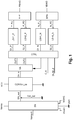
- the scheme of the figure 1 represents the polarization circuit according to the invention which is associated for example with a non-SRAM memory shown in the figure and comprising a matrix of binary storage elements, each storage element comprising at least two inverters, and each inverter comprising a PMOS transistor in series with an NMOS transistor.
- the bias circuit comprises a detection network SN comprising multiple inverters in parallel; these inverters are identical to those of the SRAM memory; they behave like those in memory with respect to their response to changes in polarization voltages.
- This detection network provides at its output SN_out a voltage value Vsn_out which represents the difference between the respective resistances of the NMOS and PMOS transistors in the inverters, that is to say the difference between the capacitances of these transistors to draw current. when their gate receives an intermediate voltage between a blocking voltage and a conduction voltage.
- this network gives an indication of the average force difference between the PMOS and NMOS transistors; for statistical reasons, this average difference represents that of the inverters of the memory to which this detection network is associated.
- This difference in average force depends on the rear biasing voltages applied to the boxes in which the transistors are built, because these rear biasing voltages act directly on the threshold voltages of the transistors.
- the rear biasing voltages NBIAS and PBIAS which are applied to the transistors of the inverters of the memory are also applied to the inverters of the detection network SN so that the detection network faithfully represents the behavior of the inverters of the memory.
- the inverters of the detection network are powered by the same general supply voltage Varray which supplies the memory points of the SRAM memory.
- the power supply is between a voltage Varray and a ground GND referenced to 0 volts.
- the voltage Varray is the reduced supply voltage (compared to the power supply voltage in the mode of normal operation) applied to the network of memory points, allowing a minimization of the consumption while ensuring a permanence of the stored information.
- the polarization circuit according to the invention will make it possible to act on the NBIAS and PBIAS rear biasing voltages of the memory in order both to minimize consumption and to guarantee a sufficient stability of the stored information.
- the inverters conventionally consist of an NMOS transistor having its source at ground, in series with a PMOS transistor having its source at Varray.
- the gates of the two transistors are combined and constitute the input of the inverter; the drains are joined and constitute the exit.
- the PMOS transistor is formed in an N-type well to which a backward bias voltage PBIAS is applied; the NMOS transistor is formed in another P type box to which a NBIAS back bias voltage is applied.
- a common voltage is applied between 0 and Varray, which will be used to evaluate the respective forces of the NMOS transistors. and PMOS.
- this reference voltage is Varray / 2. Inverters receiving on their gates this intermediate voltage tend to switch in one direction or the other depending on the respective strength of the NMOS transistor and the PMOS transistor.
- Vsn_out takes a lower value (and even close to 0) if the NMOS transistors are on average stronger; Vsn_out takes a stronger value (and even close to Varray) if the PMOS transistors are on average stronger. Even if the values of Vsn_out are not exactly 0 and Varray, Vsn_out will be considered as a low or high logic signal depending on whether Vsn_out is greater or less than Varray / 2.
- the output of the detection network SN is preferably applied to a level translator circuit CONVsn_sa which converts the level of the voltage Vsn_out, which is in the voltage range from 0 to Varray, into a logic level in a range of 0 to VDD, where VDD is the general power supply voltage of the integrated circuit.
- This translator circuit has the role of providing an output logic signal SA_in which is equal to zero or equal to VDD depending on whether the NMOS transistors are on average higher or lower than the PMOS transistors.
- CONVsn_sa which can be constituted by a simple threshold comparator whose threshold would be set between 0 and Varray (preferably Varray / 2), or which can even be deleted if the comparison with this threshold is performed. directly into the amplifier stage that follows.
- the output SA_in of this level translator circuit is connected to a sense amplifier SA, the function of which is to compare the value of the signal SA_in with a reference voltage VDD / 2 at the time of a periodic activation signal SA_clk of the following way: the amplifier SA has two outputs OUT1 and OUT2; for an idle state of the activation signal SA_clk the two outputs are pre-loaded to the same level; for an active state of the activation signal, only one of the outputs will go to zero, depending on the level of the input signal SA_in.
- the reference voltage of the SA amplifier is Varray / 2 rather than VDD / 2.
- the activation pulses SA_clk are very short, and therefore the pulses on the output OUT1 or OUT2 are very short. Their brevity makes it possible, as we will see, to periodically adjust the polarization voltages PBIAS and NBIAS by any small increments or decrements in order to guarantee the stability of the polarization.
- the pulses are at least ten times shorter than the period at which they are emitted.
- the sense amplifier therefore provides, at each cycle at the time of the clock CLK, a pulse on the output OUT1 or on the output OUT2, depending on the result of the comparison.
- a pulse on the output OUT1 will cause the incrementation of the NBIAS and PBIAS voltages.
- a pulse on the output OUT2 will cause the decrementation of these voltages.
- the outputs OUT1 and OUT2 of the amplifier SA are applied to a control circuit CTRL which also receives an authorization signal ENABLE and a clock signal CLK.
- the control circuit has two functions: first it establishes the activation signal SA_clk periodically with a period given by the clock CLK; then it establishes four logic signals S1_P, S1_N, S2_P, S2_N to level translator circuits; the two logic signals S1_P and S1_N correspond to the logic level OUT1 but are slightly delayed with respect to OUT1; these are short pulses, emitted if the sense amplifier SA has provided a pulse on OUT1.
- the two logic signals S2_P and S2_N correspond to the logical level OUT2 but are slightly delayed with respect to OUT2; they are brief pulses only if the sense amplifier has provided a pulse on OUT2. It will be seen later that the signals S1_N and S2_P can be inhibited if there is no presence of authorization by an ENABLE signal.
- the signal ENABLE is provided for example at the same time as an order to go into standby mode of the integrated circuit.
- the pulses S1_P will be used to increment the bias voltage PBIAS and at the same time the S1_N pulses will be used to increment the NBIAS polarization.
- the pulses S2_P will be used to decrement the polarization PBIAS and at the same time the S2_N pulses will be used to decrement the NBIAS polarization.
- the logic signals S1_P, S1_N, S2_P, S2_N at the output of the control circuit are in the range 0 to VDD. They are transmitted respectively to each of four level translator circuits LSH1_P, LSH1_N, LSH2_P, LSH2_N which have the following functions: they shift the output level of the signals S1_P, S1_N, S2_P, S2_N from the range 0-VDD to ranges of voltage assigned to the rear biasing voltages PBIAS and NBIAS.
- the bias voltage PBIAS must be able to vary between Varray and Varray +0.9 volts and the bias voltage NBIAS must be able to vary between 0 and -0.9 volts.
- Varray is equal to 0.2 volts, it can be envisaged that PBIAS varies between 0.9 volts and 1.1 volts.
- the level translators LSH1_P and LSH2_P provide incremental pulse logic signals P_PU and decrementation P_PD for the production of the voltage PBIAS; similarly, the level translators LSH1_N and LSH2_N provide logical signals N_PU and N_PD pulses of incrementation and decrementation for the production of NBIAS voltage.
- the signals P_PU and P_PD vary between a voltage Vlow_P and a voltage Vhigh_P, which are for example respectively Varray and Varray + 0,9volt.
- the signals N_PU and N_PD vary between a voltage Vlow_N and a voltage Vhigh_N which are for example respectively -0.9 volts and 0 volts.
- pulsed logical signals thus translated are applied to output circuits BFP and BFN which provide the bias voltages PBIAS and NBIAS.
- These output circuits are integrator circuits which integrate the small incrementation or decrementation variations imposed by the pulses applied to them.
- the pulses P_PU act to increment the voltage PBIAS
- the pulses P_PD act to decrement it.
- the signals N_PU and N_PD act one to increment, the other to decrement, the voltage NBIAS.
- the increments and decrements are small to ensure stability to bias voltages.
- a slaving of the PBIAS and NBIAS voltages thus occurs: a progressive variation of the bias voltages following the pulses in one direction will progressively increase the threshold voltage of one of the NMOS or PMOS transistors of the pair constituting an inverter and decrease that of the other.
- the signal Vsn_out will eventually switch to another logical state than the one he had before.
- This modification will reverse the pulse control signals: if the pulses came from the output OUT1, they will now go to the output OUT2 where they act in the opposite direction (decrement instead of incrementing or the opposite).
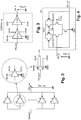
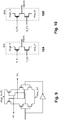
- the figure 2 represents the principle of the detector network SN: it comprises many inverters in parallel, with all their inputs combined into a common input and all their outputs combined into a common output SN_out.
- the inverters are all identical, and identical to the inverters of the SRAM memory that the bias circuit is intended to polarize.
- the inverters of the detection network are all polarized by the polarization circuit itself of which this network is a part; they are polarized in the same way as the other inverters of the integrated circuit.
- the polarization comprises the application of four potentials: the reference potential 0 of the ground GND (the reference 0 is an arbitrary reference) applied to the sources of the NMOS transistors, the potential Varray applied to the sources of the PMOS transistors, the bias voltage NBIAS applied to the P-type wells above or in which the NMOS transistors are formed, and the PBIAS voltage applied to the N-type wells above or in which the PMOS transistors are formed. It is recalled that these bias voltages affect the threshold voltages of the transistors. They therefore affect the respective conductances of the NMOS transistor and the PMOS transistor in an inverter, thus the risk of inadvertent switchover of the inverter when placing the integrated circuit in standby mode with reduced voltage Varray supply.
- the invention is applicable either to technologies in which the transistors are formed directly in boxes P-type (NMOS transistors) or N (PMOS transistors) scattered diffusers, or technologies in which the transistors are each formed above an individual box but separated from this box by other layers. In all cases, the important thing is that the bias voltage of the box influences the threshold voltage of the transistor.
- the number of inverters of the detection network is dictated by statistical considerations: it must be sufficient to correctly represent the average behavior of the inverters of the integrated circuit to be polarized. A number of one hundred will usually be sufficient. In an SRAM memory of several hundred rows and columns, it is possible to use, for example, to form the detection network, the inverters of a fictitious column (in English "dummy column") memory points, these inverters are therefore identical to inverters true memory points but connected differently.
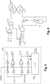
- the figure 3 represents the level translator circuit CONVsn_sa which is recalled that it is optional. It converts the voltage range from 0 to Varray from the SN array into a range of 0 to VDD, where VDD is the general power supply voltage of the integrated circuit.
- first invertor INV1 polarized like the others by the rear biasing voltages PBIAS and NBIAS, and powered between 0 and Varray.
- This inverter receives the voltage Vsn_out; it is preferably constituted by larger transistors than the very small transistors of the SRAM memory. In this way they are less sensitive to the manufacturing dispersions conventionally experienced by small transistors.
- the geometry in terms of ratio W width to length L of the transistor is however the same as that of the transistors of the inverters of the memory.
- the voltage is simply 0 or somehow Varray even if the voltage Vsn_out has a value that is not exactly one of these two values.
- the output of the inverter INV1 is connected to the input of a second inverter INV2 which is supplied between 0 and VDD and whose NMOS transistor is intrinsically much stronger than the PMOS transistor independently of the applied rear biasing voltages: the transistor NMOS has a strong W / L ratio, and the PMOS transistor a weak W / L ratio.
- the goal is to have an inverter switchover point for an input voltage lower than Varray, so that the output of this inverter represents well, but now in the range of 0-VDD voltages, the state of the input of the first inverter.
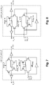
- the figure 4 represents an embodiment of the sense amplifier SA, supplied between 0 and VDD. Its input SA_in receives the output voltage Vsa_in from the circuit of the figure 3 . It also receives a reference voltage Vref and a periodic activation input SA_clk, and it has two outputs OUT1 and OUT2.
- the reference voltage is preferably VDD / 2; however, if the floor of the figure 3 was absent, this reference voltage would be then Varray / 2 (the amplifier is then powered between 0 and Varray).
- the amplifier compares the input Vsa_in with the reference voltage Vref at times determined by the periodic activation signal SA_clk.
- the activation signal SA_clk is a periodic signal which itself depends on the outputs of the amplifier; it is constituted by a very brief periodic pulse during which the comparison is made.
- the outputs OUT1 and OUT2 are both at the same level, here a high level VDD.
- the outputs are identical when the clock is low and complementary when it is high.
- the output OUT1 goes low when the voltage Vsa_in is greater than Vref, therefore when the output voltage Vsn_out of the detection network is close to Varray; conversely, OUT2 goes low when Vsn_out is close to zero.
- the figure 5 represents the control circuit CTRL. This circuit receives a periodic clock signal CLK, an authorization signal ENABLE, and the logic signals of the outputs OUT1 and OUT2 of the detection amplifier.
- the signal ENABLE can come for example from a standby order.
- the control circuit comprises logic gates which process the signals OUT1 and OUT2 in a manner to be indicated, and a clock transition detection circuit CEDC which produces the pulse activation signal SA_clk from the signal d periodic clock CLK and from signals OUT1 and OUT2.
- the ENABLE signal is active at low level. It allows outputs S1_N and S2_P respectively to supply the logical values present on OUT1 and OUT2. At the high level, the signal ENABLE forces the signals S1_N and S2_P to zero, the consequence being that the bias circuit no longer performs its regulation function of NBIAS and PBIAS but forces NBIAS and PBIAS to nominal values which are preferably zero. for NBIAS and Varray for PBIAS.
- the zero crossing pulses of OUT1 are transferred to the outputs S1_N and S1_P; the OUT2 pulses are reported on the outputs S2_N and S2_P.
- the signals on the outputs S1_N and S2_N serve as a control for the detection circuit of clock transitions CEDC.
- This circuit periodically produces a very short pulse SA_clk during which the comparison is carried out in the detection amplifier.
- the circuit CEDC receives for this purpose the periodic clock CLK whose high and low slots are of identical duration. It also receives the ENABLE signal and here again we consider the case where ENABLE is active (standby mode), therefore at the low level. If ENABLE was inactive (high level) the circuit would not produce SA_clk pulses.
- the clock transition detection circuit is represented at the figure 6 .
- An AND gate 10 transmits the clock CLK and its delayed complement by one or more inverters in series to the inputs of another AND gate 12 so as to produce a short trigger pulse on the rising edge of the clock signal; this pulse, applied to a first input of a RS flip-flop (consisting of two NI gates 14 and 16 looped one over the other), switches the flip-flop, causing the output signal SA_clk to go high, initially at low level.
- the comparison process is then done in the sense amplifier during this brief pulse.
- One of the signals OUT1 or OUT2 will therefore go to zero during this pulse.
- the signals S1_N and S2_N (corresponding to signals OUT1 and OUT2 but slightly delayed) are applied to the inputs of an exclusive-OR gate 18 which supplies a logic signal in general which is zero when S1_N and S2_N are both at level 1 and which provides a logic signal high when either of OUT1 and OUT2 goes to zero.
- the passage to the high level of the output of the gate 18 makes again switch the flip-flop 14, 16 which reduces to zero the SA_clk signal, interrupting the activation signal which is very brief.
- the signal OUT1 or OUT2 which has passed to the low level returns to the high level imposed by the interruption of the activation signal; the signals S1_N, S1_P, S2_N, S2_P all return to the high level again.
- An OR gate 20 receives the ENABLE signal to block the flip-flop with SA_clk at the low level when ENABLE is at the inactive level (high level) to prohibit the servocontrol of the bias voltages.
- the pulse serves, in the manner of a charge pump, to increment or decrement the average voltage PBIAS or NBIAS by injecting a short charge or discharge current for the duration of the pulse. It is the overall natural capacity of the regions polarized by the PBIAS and NBIAS voltages that keeps the bias voltage at a mean value between two pulses.
- the signals S1_N, S1_P, S2_N, S2_P are between 0 (low level) and VDD (high level). They must be brought back to a voltage range corresponding to the voltage range in which the NBIAS and PBIAS voltages can evolve.
- the voltage Varray is 0.2 volts and it is desired that the rear biasing voltages can vary between 0 volts and -0.9 volts for NBIAS and between 0.2 volts and 1.1 volts for PBIAS.
- the figure 7 represents the configuration of a LSH1_P level translator which can be used for translation to higher potentials. It receives the pulse S1_P and provides a pulse P_PU on one of its outputs; the pulse P_PU is an incrementation pulse of the voltage PBIAS and it must be, as will be seen, a pulse of passage to the low logical level because it controls a PMOS transistor.
- the circuit LSH1_P has a second output referenced P_PD, logical complement of the first, but which is not used.
- the level translator LSH2_P is strictly identical but it receives the pulse S2_P and it uses the second output P_PD and not the first; in fact, it must produce a pulse of decrementation of the voltage PBIAS and this pulse must be a pulse of passage to the logic high level because it controls an NMOS transistor.
- Vhigh_P and Vlow_P have been called voltage sources for transposing the pulse levels to the voltage range from Vlow_P to Vhigh_P.
- the zero reference potential is used in this scheme.
- Vlow_P is in principle equal to Varray;
- Vhigh_P can be equal to Varray + 0.9 volts.
- figure 8 represents a level translator LSH1_N for a translation to lower potentials. It receives the pulse S1_N and provides an N_PU pulse on one of its outputs (low-pass pulse for the control of a PMOS transistor incrementation of NBIAS); it has a complementary logical output N_PD which is not used.
- the translator LSH2_N is identical, it receives the pulse S2_N and it provides a pulse on the second output N_PD and not the first (high-pass pulse for the control of a NMOS transistor decrementation of NBIAS).
- Vhigh_N is in principle equal to 0; Vlow_N can be equal to -0.9 volts.
- the figure 9 is another example of a level translator circuit that can be used for both upward and downward level translation.
- figure 10 represents the two integrator stages of output BFP and BFN supplying the voltages PBIAS and NBIAS. These are stages each comprising an NMOS transistor in series with a PMOS transistor. These series assemblies are powered by the potentials Vhigh_P and Vlow_P for the stage supplying the potential PBIAS ( figure 10A ) or by the potentials Vhigh_N and Vlow_N for the stage supplying the potential NBIAS ( figure 10B ).
- the pulses of the P_PU and P_PD outputs of the level translators are respectively applied to the gate of the PMOS transistor and to the gate of the NMOS transistor for the stage which supplies the bias voltage PBIAS.
- the logic levels N_PU and N_PD are applied to the gates of the transistors of the stage which supplies the bias voltage PBIAS.
- the pulse P_PU (incrementation of PBIAS) is a zero crossing pulse (Vlow_P) and briefly turns on the PMOS transistor.
- the pulse P_PD (decrementation of PBIAS) is a high-pass pulse (Vhigh_P) and briefly turns on the NMOS transistor.
- the pulse N_PU (incrementation of NBIAS) is a high-pass pulse (Vhigh_N) and briefly turns on the PMOS transistor.
- the pulse N_PD (decrementation of NBIAS) is a low-pass pulse (Vlow_N) and briefly turns on the NMOS transistor.
Landscapes
- Engineering & Computer Science (AREA)
- Microelectronics & Electronic Packaging (AREA)
- Computer Hardware Design (AREA)
- Power Engineering (AREA)
- Logic Circuits (AREA)
Description
L'invention concerne les circuits intégrés CMOS à très faible consommation, et notamment les mémoires volatiles SRAM.The invention relates to CMOS integrated circuits with very low consumption, and in particular volatile memories SRAM.
Des circuits intégrés de plus en plus complexes sont utilisés dans des applications où la disponibilité d'énergie est très limitée. C'est le cas des téléphones portables, des ordinateurs de poche, et autres appareils électroniques alimentés par des batteries. Il est important de minimiser leur consommation par tous les moyens possibles si on veut disposer d'une autonomie de fonctionnement suffisante. Or, les circuits intégrés consomment d'autant plus de puissance qu'ils comportent un plus grand nombre de transistors, et on fait aujourd'hui des circuits intégrés comportant des centaines de millions, voire des milliards de transistors. Des mémoires volatiles de type SRAM sont en particulier utilisées dans ces appareils, et leur capacité peut atteindre des millions ou milliards de points-mémoire, chaque point mémoire ayant par exemple six transistors.Increasingly complex integrated circuits are used in applications where the availability of energy is very limited. This is the case for mobile phones, handheld computers, and other electronic devices powered by batteries. It is important to minimize their consumption by all possible means if we want to have sufficient autonomy of operation. However, integrated circuits consume more power than they contain a greater number of transistors, and today we make integrated circuits with hundreds of millions, even billions of transistors. Volatile memories of the SRAM type are in particular used in these devices, and their capacity can reach millions or billions of memory points, each memory point having for example six transistors.
Les mémoires statiques SRAM doivent être alimentées en énergie même en dehors des moments d'utilisation pour pouvoir conserver leur contenu entre deux utilisations. Si l'alimentation est coupée, l'information mémorisée disparaît. Comme les phases de non-utilisation peuvent parfois être beaucoup plus longues que les phases d'utilisation, il faut faire tout spécialement attention à minimiser la consommation pendant les phases de non-utilisation.SRAM static memory must be powered even outside of the time of use in order to keep its contents between two uses. If the power is turned off, the stored information disappears. Since the non-use phases can sometimes be much longer than the use phases, special attention must be paid to minimizing consumption during the non-use phases.
De manière générale, il est courant de réduire la tension d'alimentation des circuits intégrés, et notamment des mémoires SRAM dans un mode de veille entre deux utilisations ; on rétablit ensuite la tension normale, permettant un fonctionnement actif de la mémoire en lecture ou écriture lorsqu'on veut à nouveau utiliser l'appareil. Mais il faut quand même conserver une tension d'alimentation suffisante en mode de veille pour garantir le maintien de l'information stockée en mémoire. La limite de cette méthode se trouve donc dans le choix d'une tension de veille bien adaptée, à la fois suffisamment faible pour limiter la consommation et suffisante pour garantir le maintien de l'information stockée.In general, it is common to reduce the supply voltage of the integrated circuits, including SRAMs in a sleep mode between two uses; the normal voltage is then restored, allowing active operation of the read or write memory when the device is to be used again. But it is still necessary to maintain a sufficient supply voltage in standby mode to ensure the maintenance of the information stored in memory. The limit of this method is therefore in the choice of a well adapted standby voltage, both low enough to limit consumption and sufficient to ensure the maintenance of the stored information.
On a également proposé de modifier les tensions de polarisation de face arrière du substrat de circuit intégré en fonction de l'utilisation plus ou moins active de l'appareil : mode normal, mode de veille, ou même mode de fonctionnement accéléré.It has also been proposed to modify the rear-face biasing voltages of the integrated circuit substrate according to the more or less active use of the apparatus: normal mode, standby mode, or even accelerated mode of operation.
La publication de brevet
La présente invention vise à améliorer les possibilités de réduction de la consommation en mode de veille par une action adaptative sur la tension de polarisation arrière des caissons des transistors NMOS et PMOS qui composent les inverseurs utilisés dans le circuit.The present invention aims to improve the possibilities of reducing the consumption in standby mode by an adaptive action on the back bias voltage of the boxes of the NMOS and PMOS transistors that make up the inverters used in the circuit.
L'invention s'applique donc à des circuits intégrés dont les transistors NMOS, formés dans des caissons ou au-dessus de caissons dopés de type P, et les transistors PMOS, formés dans des caissons ou au-dessus de caissons dopés de type N, reçoivent des tensions de polarisation arrière distinctes NBIAS et PBIAS. Un circuit de polarisation établit ces tensions de polarisation notamment sur les inverseurs à deux transistors d'une mémoire SRAM, à partir d'un réseau de détection qui comprend de nombreux transistors NMOS et PMOS ; le comportement moyen de ces transistors varie en fonction des tensions de polarisation, en raison du fait que ces tensions tendent à modifier les tensions de seuil de mise en conduction des transistors ; on agit sur les tensions de polarisation de manière à s'approcher d'un comportement optimal désiré. Le comportement optimal est de préférence un comportement dans lequel les transistors NMOS et PMOS sont équilibrés. Par transistors équilibrés, on entend le fait qu'une même tension de référence, de préférence égale à la moitié de la tension d'alimentation Varray des inverseurs qui sont à polariser, appliquée à la grille d'un transistor NMOS et appliquée à la grille d'un transistor PMOS tend à faire circuler des courants identiques dans les deux transistors.The invention therefore applies to integrated circuits whose NMOS transistors, formed in boxes or above P-type doped wells, and the PMOS transistors, formed in wells or above N-type doped wells. , receive separate back bias voltages NBIAS and PBIAS. A bias circuit establishes these bias voltages, in particular on the two-transistor inverters of an SRAM, from a detection network which comprises numerous NMOS and PMOS transistors; the average behavior of these transistors varies as a function of the bias voltages, due to the fact that these voltages tend to modify the conduction threshold voltages of the transistors; the polarization voltages are acted upon so as to approach a desired optimal behavior. The optimal behavior is preferably a behavior in which the NMOS and PMOS transistors are balanced. By balanced transistors is meant the fact that the same reference voltage, preferably equal to half of the Varray supply voltage of the inverters that are to be biased, applied to the gate of an NMOS transistor and applied to the gate of a PMOS transistor tends to circulate identical currents in the two transistors.
Par conséquent, l'invention propose un circuit de polarisation des inverseurs d'un circuit intégré, chaque inverseur comprenant un transistor NMOS et un transistor PMOS alimentés par une tension d'alimentation Varray, avec des moyens pour appliquer une première tension de polarisation arrière NBIAS aux caissons des transistors NMOS et une deuxième tension de polarisation arrière PBIAS aux caissons des transistors PMOS, le circuit de polarisation selon l'invention fournissant ces tensions de polarisation et comprenant :
- un réseau de détection comprenant pluralité d' inverseurs montés en parallèle, les inverseurs étant alimentés par la tension d'alimentation Varray et polarisés par les deux tensions de polarisation arrière et recevant sur leur grilles une même tension de référence comprise entre 0 et la tension d'alimentation Varray des inverseurs, la sortie commune des inverseurs constituant la sortie du réseau de détection, cette sortie fournissant un signal logique dont la valeur dépend des tensions de polarisation arrière appliquées au réseau,
- un circuit de production d'impulsions d'incrémentation ou décrémentation, commandé en fonction de la tension de sortie du réseau de détection,
- et un circuit d'intégration relié au circuit de production d'impulsions, pour produire et faire varier progressivement par incréments en réponse à ces impulsions, la première tension de polarisation arrière NBIAS et la deuxième tension de polarisation arrière PBIAS dans un sens tendant à inverser le niveau du signal logique de sortie du réseau de détecteur.
- a detection network comprising a plurality of inverters connected in parallel, the inverters being powered by the supply voltage Varray and biased by the two rear biasing voltages and receiving on their gates the same reference voltage of between 0 and the voltage d Varrier supply of the inverters, the common output of the inverters constituting the output of the detection network, this output providing a logic signal whose value depends on the rear biasing voltages applied to the network,
- an incrementation or decrement pulse generation circuit, controlled as a function of the output voltage of the detection network,
- and an integrating circuit connected to the pulse generating circuit, for producing and progressively varying in increments in response to these pulses, the first rear biasing voltage NBIAS and the second rear biasing voltage PBIAS in a direction tending to reverse the level of the logic output signal of the detector array.
La tension de référence appliquée à l'entrée des inverseurs du réseau de détection est de préférence Varray/2.The reference voltage applied to the input of the inverters of the detection network is preferably Varray / 2.
Un circuit de translation de niveau logique peut être interposé entre la sortie du réseau de détection et l'entrée du circuit de production d'impulsions.A logic level translation circuit can be interposed between the output of the detection network and the input of the pulse generating circuit.
Le circuit de production d'impulsions peut comprendre un amplificateur de détection et un circuit de contrôle, le circuit de contrôle comportant un circuit d'horloge produisant périodiquement un signal d'activation constitué par des impulsions brèves servant à l'activation de l'amplificateur de détection, l'amplificateur de détection recevant une tension issue du réseau de détection et agissant comme un comparateur par rapport à une tension de référence pour produire sur l'une de deux sorties (OUT1, OUT2), en fonction du résultat de la comparaison, une impulsion de commande.The pulse generating circuit may comprise a sense amplifier and a control circuit, the control circuit having a clock circuit periodically producing an activation signal consisting of short pulses for the activation of the sense amplifier, the sense amplifier receiving a voltage derived from the detection network and acting as a comparator with respect to a reference voltage for producing on one of two outputs (OUT1, OUT2), depending on the result of the comparison, a control pulse.
Le circuit de contrôle reçoit les deux sorties de l'amplificateur de détection et il produit quatre signaux impulsionnels correspondants en fonction des résultats de la comparaison ; ces signaux constituent des impulsions d'incrémentation et de décrémentation des tensions NBIAS et BPIAS respectivement ; ces impulsions sont transmises respectivement à quatre circuits translateurs de niveau, deux premiers circuits translateurs de niveau convertissant deux des signaux impulsionnels dans une plage de tensions correspondant à une plage de variation de tension désirée pour la tension de polarisation PBIAS, et deux autres circuits translateurs de niveau convertissant les deux autres signaux impulsionnels dans une plage de tensions correspondant à une plage de variation de tension désirée pour la tension de polarisation NBIAS.The control circuit receives the two outputs of the sense amplifier and produces four corresponding pulse signals according to the results of the comparison; these signals constitute incrementing and decrementing pulses NBIAS and BPIAS respectively; these pulses are respectively transmitted to four level translator circuits, two first level translator circuits converting two of the pulse signals into a voltage range corresponding to a desired voltage variation range for the bias voltage PBIAS, and two other translating circuits of level converting the other two pulse signals into a voltage range corresponding to a desired voltage variation range for the NBIAS bias voltage.
Le circuit d'intégration comprend de préférence un premier circuit pour produire la tension de polarisation PBIAS et un deuxième circuit pour produire la tension de polarisation NBIAS, le premier circuit recevant sur ses entrées les sorties de deux premiers circuits translateurs de niveau, et le deuxième circuit recevant sur ses entrées les sorties des deux autres circuits translateurs de niveau.The integration circuit preferably comprises a first circuit for producing the bias voltage PBIAS and a second circuit for producing the bias voltage NBIAS, the first circuit receiving on its inputs the outputs of two first level translator circuits, and the second circuit circuit receiving at its inputs the outputs of the two other level translator circuits.
Le premier circuit et le deuxième circuits peuvent être réalisés très simplement à partir de deux transistors en série, un transistor PMOS et un transistor NMOS, qui reçoivent sur leurs grilles les sorties des circuits translateurs de niveau. Pour le premier circuit, l'ensemble de deux transistors en série est alimenté entre une tension basse (Vlow_P) et une tension haute (Vhigh_P) correspondant à la plage de tensions désirée pour la variation de la tension PBIAS. Pour le deuxième circuit, l'ensemble de transistors en série du deuxième circuit étant alimenté entre une tension basse (Vlow_N) et une tension haute (Vhigh_N) correspondant à la plage de tensions désirée pour la variation de la tension NBIAS. Dans les deux circuits, la tension de polarisation (PBIAS ou NBIAS) est fournie au point de jonction du transistor NMOS et du transistor PMOS.The first circuit and the second circuit can be made very simply from two series transistors, a PMOS transistor and an NMOS transistor, which receive on their gates the outputs of the level translator circuits. For the first circuit, the set of two series transistors is supplied between a low voltage (Vlow_P) and a high voltage (Vhigh_P) corresponding to the desired voltage range for the variation of the voltage PBIAS. For the second circuit, the set of series transistors of the second circuit being fed between a low voltage (Vlow_N) and a high voltage (Vhigh_N) corresponding to the desired voltage range for the variation of the NBIAS voltage. In both circuits, the bias voltage (PBIAS or NBIAS) is provided at the junction point of the NMOS transistor and the PMOS transistor.
En général (mais pas obligatoirement), le circuit de polarisation comprendra une entrée d'autorisation qui autorise ou interdit l'application d'impulsions d'incrémentation ou décrémentation au circuit d'intégration, et on s'en servira notamment pour autoriser cette application en mode de veille avec alimentation en tension réduite du circuit intégré (notamment de la mémoire SRAM).In general (but not necessarily), the bias circuit will include an authorization input that allows or prohibits the application of incrementation or decrement pulses to the integration circuit, and will be used in particular to allow this application in standby mode with reduced voltage supply of the integrated circuit (in particular the SRAM).
D'autres caractéristiques et avantages de l'invention apparaîtront à la lecture de la description détaillée qui suit et qui est faite en référence aux dessins annexés dans lesquels :
- la
figure 1 représente l'architecture générale du circuit de polarisation selon l'invention ; - la
figure 2 représente la constitution du réseau de détection composé de multiples inverseurs en parallèle ; - la
figure 3 représente un étage de conversion de niveau logique (facultatif) en sortie du réseau de détection ; - la
figure 4 représente la constitution de l'amplificateur de détection ; - la
figure 5 représente le circuit de contrôle qui génère quatre signaux impulsionnels complémentaires et qui génère aussi de brèves impulsions d'activation à destination de l'amplificateur de détection ; - la
figure 6 représente le circuit qui produit les brèves impulsions d'activation ; - la
figure 7 représente un circuit translateur de niveau pour transposer les signaux logiques vers une plage de tensions plus élevée ; - la
figure 8 représente un circuit translateur de niveau pour transposer les signaux logiques vers une plage de tensions plus basse ; - la
figure 9 représente une variante de circuit translateur de niveau ; - la
figure 10 représente le circuit d'intégration qui produit les tensions PBIAS et NBIAS à partir des impulsions d'incrémentation ou de décrémentation reçues.
- the
figure 1 represents the general architecture of the polarization circuit according to the invention; - the
figure 2 represents the constitution of the detection network composed of multiple inverters in parallel; - the
figure 3 represents a logical level conversion stage (optional) at the output of the detection network; - the
figure 4 represents the constitution of the sense amplifier; - the
figure 5 represents the control circuit which generates four complementary pulse signals and which also generates brief activation pulses to the sense amplifier; - the
figure 6 represents the circuit that produces the brief activation pulses; - the
figure 7 represents a level translator circuit for transposing the logic signals to a higher voltage range; - the
figure 8 represents a level translator circuit for transposing the logic signals to a lower voltage range; - the
figure 9 represents a variant of a level translator circuit; - the
figure 10 represents the integration circuit that produces the PBIAS and NBIAS voltages from the incrementing or decrementing pulses received.
Le schéma de la
Le circuit de polarisation comporte un réseau de détection SN comprenant de multiples inverseurs en parallèle ; ces inverseurs sont identiques à ceux de la mémoire SRAM ; ils se comportent donc comme ceux de la mémoire en ce qui concerne leur réponse à des changements de tensions de polarisation. Ce réseau de détection fournit sur sa sortie SN_out une valeur de tension Vsn_out qui représente la différence entre les résistances respectives des transistors NMOS et PMOS dans les inverseurs, c'est-à-dire la différence entre les aptitudes de ces transistors à tirer du courant lorsque leur grille reçoit une tension intermédiaire entre une tension de blocage et une tension de mise en conduction. En utilisant de multiples inverseurs, au moins vingt et de préférence cent ou plus), ce réseau donne une indication de la différence de force moyenne entre les transistors PMOS et NMOS ; pour des raisons statistiques, cette différence moyenne représente celle des inverseurs de la mémoire à laquelle ce réseau de détection est associé. Cette différence de force moyenne dépend des tensions de polarisation arrière appliquées aux caissons dans lesquels sont construits les transistors, car ces tensions de polarisation arrière agissent directement sur les tensions de seuil des transistors. Les tensions de polarisation arrière NBIAS et PBIAS qui sont appliquées aux transistors des inverseurs de la mémoire sont également appliquées aux inverseurs du réseau de détection SN afin que le réseau de détection représente fidèlement le comportement des inverseurs de la mémoire. De même, les inverseurs du réseau de détection sont alimentés par la même tension d'alimentation générale Varray qui alimente les points-mémoire de la mémoire SRAM.The bias circuit comprises a detection network SN comprising multiple inverters in parallel; these inverters are identical to those of the SRAM memory; they behave like those in memory with respect to their response to changes in polarization voltages. This detection network provides at its output SN_out a voltage value Vsn_out which represents the difference between the respective resistances of the NMOS and PMOS transistors in the inverters, that is to say the difference between the capacitances of these transistors to draw current. when their gate receives an intermediate voltage between a blocking voltage and a conduction voltage. Using multiple inverters, at least twenty, preferably one hundred or more), this network gives an indication of the average force difference between the PMOS and NMOS transistors; for statistical reasons, this average difference represents that of the inverters of the memory to which this detection network is associated. This difference in average force depends on the rear biasing voltages applied to the boxes in which the transistors are built, because these rear biasing voltages act directly on the threshold voltages of the transistors. The rear biasing voltages NBIAS and PBIAS which are applied to the transistors of the inverters of the memory are also applied to the inverters of the detection network SN so that the detection network faithfully represents the behavior of the inverters of the memory. Similarly, the inverters of the detection network are powered by the same general supply voltage Varray which supplies the memory points of the SRAM memory.
On considérera ci-après que l'alimentation se fait entre une tension Varray et une masse GND référencée à 0 volt.It will be considered below that the power supply is between a voltage Varray and a ground GND referenced to 0 volts.
Dans ce qui suit on s'intéresse principalement au cas où la mémoire fonctionne en mode de veille, et la tension Varray est la tension d'alimentation réduite (par rapport à la tension d'alimentation en mode de fonctionnement normal) appliquée au réseau de points mémoire, permettant une minimisation de la consommation tout en assurant une permanence de l'information stockée. Le circuit de polarisation selon l'invention va permettre d'agir sur les tensions de polarisation arrière NBIAS et PBIAS de la mémoire pour à la fois minimiser la consommation et garantir une stabilité suffisante de l'information stockée.In what follows, we are mainly interested in the case where the memory operates in standby mode, and the voltage Varray is the reduced supply voltage (compared to the power supply voltage in the mode of normal operation) applied to the network of memory points, allowing a minimization of the consumption while ensuring a permanence of the stored information. The polarization circuit according to the invention will make it possible to act on the NBIAS and PBIAS rear biasing voltages of the memory in order both to minimize consumption and to guarantee a sufficient stability of the stored information.
Les inverseurs sont classiquement constitués par un transistor NMOS ayant sa source à la masse, en série avec un transistor PMOS ayant sa source à Varray. Les grilles des deux transistors sont réunies et constituent l'entrée de l'inverseur ; les drains sont réunis et constituent la sortie. Le transistor PMOS est formé dans un caisson de type N auquel on applique une tension de polarisation arrière PBIAS ; le transistor NMOS est formé dans un autre caisson de type P auquel on applique une tension de polarisation arrière NBIAS.The inverters conventionally consist of an NMOS transistor having its source at ground, in series with a PMOS transistor having its source at Varray. The gates of the two transistors are combined and constitute the input of the inverter; the drains are joined and constitute the exit. The PMOS transistor is formed in an N-type well to which a backward bias voltage PBIAS is applied; the NMOS transistor is formed in another P type box to which a NBIAS back bias voltage is applied.
On applique à l'entrée de tous les inverseurs du réseau de détection, sur les grilles réunies des transistors NMOS et PMOS qui constituent ce réseau, une tension commune, intermédiaire entre 0 et Varray, qui va servir à évaluer les forces respectives des transistors NMOS et PMOS. De préférence cette tension de référence est Varray/2. Les inverseurs recevant sur leurs grilles cette tension intermédiaire ont tendance à basculer dans un sens ou dans l'autre selon la force respective du transistor NMOS et du transistor PMOS. Globalement, la tension de sortie du réseau de multiples inverseurs en parallèle tend à prendre une valeur Vsn_out qui découle de cette différence entre les forces des transistors NMOS et PMOS : Vsn_out prend une valeur plus faible (et même proche de 0) si les transistors NMOS sont en moyenne plus forts ; Vsn_out prend une valeur plus forte (et même proche de Varray) si les transistors PMOS sont en moyenne plus forts. Même si les valeurs de Vsn_out ne sont pas exactement 0 et Varray, on considérera que Vsn_out est un signal logique de niveau bas ou de niveau haut selon que Vsn_out est supérieur ou inférieur à Varray/2.At the input of all the inverters of the detection network, on the combined gates of the NMOS and PMOS transistors which constitute this network, a common voltage is applied between 0 and Varray, which will be used to evaluate the respective forces of the NMOS transistors. and PMOS. Preferably this reference voltage is Varray / 2. Inverters receiving on their gates this intermediate voltage tend to switch in one direction or the other depending on the respective strength of the NMOS transistor and the PMOS transistor. Overall, the output voltage of the network of multiple inverters in parallel tends to take a value Vsn_out which results from this difference between the forces of the NMOS and PMOS transistors: Vsn_out takes a lower value (and even close to 0) if the NMOS transistors are on average stronger; Vsn_out takes a stronger value (and even close to Varray) if the PMOS transistors are on average stronger. Even if the values of Vsn_out are not exactly 0 and Varray, Vsn_out will be considered as a low or high logic signal depending on whether Vsn_out is greater or less than Varray / 2.
La sortie du réseau de détection SN est appliquée de préférence à un circuit translateur de niveau CONVsn_sa qui convertit le niveau de la tension Vsn_out, qui est dans la gamme de tension de 0 à Varray, en un niveau logique dans une gamme de 0 à VDD, où VDD est la tension d'alimentation générale du circuit intégré. Ce circuit translateur a pour rôle de fournir un signal logique de sortie SA_in qui est égale à zéro ou égale à VDD selon que les transistors NMOS sont en moyenne plus forts ou plus faibles que les transistors PMOS. On reviendra plus loin sur ce circuit translateur CONVsn_sa qui peut être constitué par un simple comparateur à seuil dont le seuil serait fixé entre 0 et Varray (de préférence Varray/2), ou qui peut même être supprimé si la comparaison avec ce seuil est effectuée directement dans l'étage amplificateur qui suit.The output of the detection network SN is preferably applied to a level translator circuit CONVsn_sa which converts the level of the voltage Vsn_out, which is in the voltage range from 0 to Varray, into a logic level in a range of 0 to VDD, where VDD is the general power supply voltage of the integrated circuit. This translator circuit has the role of providing an output logic signal SA_in which is equal to zero or equal to VDD depending on whether the NMOS transistors are on average higher or lower than the PMOS transistors. We will return later to this translator circuit CONVsn_sa which can be constituted by a simple threshold comparator whose threshold would be set between 0 and Varray (preferably Varray / 2), or which can even be deleted if the comparison with this threshold is performed. directly into the amplifier stage that follows.
La sortie SA_in de ce circuit translateur de niveau est connectée à un amplificateur de détection SA, dont la fonction est de comparer la valeur du signal SA_in à une tension de référence VDD/2 au moment d'un signal d'activation périodique SA_clk de la manière suivante : l'amplificateur SA a deux sorties OUT1 et OUT2 ; pour un état inactif du signal d'activation SA_clk les deux sorties sont pré-chargées à un même niveau ; pour un état actif du signal d'activation, l'une des sorties seulement passera à zéro, selon le niveau du signal d'entrée SA_in. Dans le cas où on ne prévoit pas d'étage translateur de niveau CONVsn_sa, la tension de référence de l'amplificateur SA est Varray/2 plutôt que VDD/2.The output SA_in of this level translator circuit is connected to a sense amplifier SA, the function of which is to compare the value of the signal SA_in with a reference voltage VDD / 2 at the time of a periodic activation signal SA_clk of the following way: the amplifier SA has two outputs OUT1 and OUT2; for an idle state of the activation signal SA_clk the two outputs are pre-loaded to the same level; for an active state of the activation signal, only one of the outputs will go to zero, depending on the level of the input signal SA_in. In the case where a CONVsn_sa level translator stage is not provided, the reference voltage of the SA amplifier is Varray / 2 rather than VDD / 2.
Les impulsions d'activation SA_clk sont très brèves, et par conséquent, les impulsions sur la sortie OUT1 ou OUT2 sont très brèves. Leur brièveté permet, comme on le verra, d'ajuster périodiquement les tensions de polarisation PBIAS et NBIAS par tout petits incréments ou décréments afin de garantir la stabilité de la polarisation. De préférence les impulsions sont au moins dix fois plus courtes que la période à laquelle elles sont émises.The activation pulses SA_clk are very short, and therefore the pulses on the output OUT1 or OUT2 are very short. Their brevity makes it possible, as we will see, to periodically adjust the polarization voltages PBIAS and NBIAS by any small increments or decrements in order to guarantee the stability of the polarization. Preferably the pulses are at least ten times shorter than the period at which they are emitted.
L'amplificateur de détection fournit donc, à chaque cycle à la période de l'horloge CLK, une impulsion sur la sortie OUT1 ou sur la sortie OUT2, dépendant du résultat de la comparaison. Une impulsion sur la sortie OUT1 provoquera l'incrémentation des tensions NBIAS et PBIAS. Une impulsion sur la sortie OUT2 provoquera la décrémentation de ces tensions.The sense amplifier therefore provides, at each cycle at the time of the clock CLK, a pulse on the output OUT1 or on the output OUT2, depending on the result of the comparison. A pulse on the output OUT1 will cause the incrementation of the NBIAS and PBIAS voltages. A pulse on the output OUT2 will cause the decrementation of these voltages.
Les sorties OUT1 et OUT2 de l'amplificateur SA sont appliquées à un circuit de contrôle CTRL qui reçoit en outre un signal d'autorisation ENABLE et un signal d'horloge CLK. Le circuit de contrôle a deux fonctions : d'abord il établit le signal d'activation SA_clk périodiquement avec une période donnée par l'horloge CLK ; ensuite il établit quatre signaux logiques S1_P, S1_N, S2_P, S2_N à destination de circuits translateurs de niveau ; les deux signaux logiques S1_P et S1_N correspondent au niveau logique OUT1 mais sont légèrement retardés par rapport à OUT1 ; ce sont des impulsions brèves, émises si l'amplificateur de détection SA a fourni une impulsion sur OUT1. De même, les deux signaux logiques S2_P et S2_N correspondent au niveau logique OUT2 mais sont légèrement retardés par rapport à OUT2 ; ce sont des impulsions brèves émises seulement si l'amplificateur de détection a fourni une impulsion sur OUT2. On verra plus loin que les signaux S1_N et S2_P peuvent être inhibés s'il n'y a pas la présence d'une autorisation par un signal ENABLE. Le signal ENABLE est fourni par exemple en même temps qu'un ordre de passage en mode de veille du circuit intégré.The outputs OUT1 and OUT2 of the amplifier SA are applied to a control circuit CTRL which also receives an authorization signal ENABLE and a clock signal CLK. The control circuit has two functions: first it establishes the activation signal SA_clk periodically with a period given by the clock CLK; then it establishes four logic signals S1_P, S1_N, S2_P, S2_N to level translator circuits; the two logic signals S1_P and S1_N correspond to the logic level OUT1 but are slightly delayed with respect to OUT1; these are short pulses, emitted if the sense amplifier SA has provided a pulse on OUT1. Likewise, the two logic signals S2_P and S2_N correspond to the logical level OUT2 but are slightly delayed with respect to OUT2; they are brief pulses only if the sense amplifier has provided a pulse on OUT2. It will be seen later that the signals S1_N and S2_P can be inhibited if there is no presence of authorization by an ENABLE signal. The signal ENABLE is provided for example at the same time as an order to go into standby mode of the integrated circuit.
Les impulsions S1_P vont servir à incrémenter la tension de polarisation PBIAS et en même temps les impulsions S1_N vont servir à incrémenter la polarisation NBIAS. Les impulsions S2_P vont servir à décrémenter la polarisation PBIAS et en même temps les impulsions S2_N vont servir à décrémenter la polarisation NBIAS.The pulses S1_P will be used to increment the bias voltage PBIAS and at the same time the S1_N pulses will be used to increment the NBIAS polarization. The pulses S2_P will be used to decrement the polarization PBIAS and at the same time the S2_N pulses will be used to decrement the NBIAS polarization.
Les signaux logiques S1_P, S1_N, S2_P, S2_N en sortie du circuit de contrôle sont dans la plage 0 à VDD. Ils sont transmis respectivement à chacun de quatre circuits translateurs de niveau LSH1_P, LSH1_N, LSH2_P, LSH2_N qui ont les fonctions suivantes : ils décalent le niveau de sortie des signaux S1_P, S1_N, S2_P, S2_N de la plage 0-VDD vers des plages de tension attribuées aux tensions de polarisation arrière PBIAS et NBIAS. Par exemple, la tension de polarisation PBIAS doit pouvoir varier entre Varray et Varray+0,9 volt et la tension de polarisation NBIAS doit pouvoir varier entre 0 et -0,9 volt. Par exemple, si Varray est égal à 0,2 volt, on peut envisager que PBIAS varie entre 0,9 volt et 1,1 volt.The logic signals S1_P, S1_N, S2_P, S2_N at the output of the control circuit are in the range 0 to VDD. They are transmitted respectively to each of four level translator circuits LSH1_P, LSH1_N, LSH2_P, LSH2_N which have the following functions: they shift the output level of the signals S1_P, S1_N, S2_P, S2_N from the range 0-VDD to ranges of voltage assigned to the rear biasing voltages PBIAS and NBIAS. For example, the bias voltage PBIAS must be able to vary between Varray and Varray +0.9 volts and the bias voltage NBIAS must be able to vary between 0 and -0.9 volts. For example, if Varray is equal to 0.2 volts, it can be envisaged that PBIAS varies between 0.9 volts and 1.1 volts.
Ainsi, les translateurs de niveau LSH1_P et LSH2_P fournissent des signaux logiques impulsionnels d'incrémentation P_PU et de décrémentation P_PD pour la production de la tension PBIAS ; de même, les translateurs de niveau LSH1_N et LSH2_N fournissent des signaux logiques impulsionnels N_PU et N_PD d'incrémentation et de décrémentation pour la production de la tension NBIAS.Thus, the level translators LSH1_P and LSH2_P provide incremental pulse logic signals P_PU and decrementation P_PD for the production of the voltage PBIAS; similarly, the level translators LSH1_N and LSH2_N provide logical signals N_PU and N_PD pulses of incrementation and decrementation for the production of NBIAS voltage.
Les signaux P_PU et P_PD varient entre une tension Vlow_P et une tension Vhigh_P, qui sont par exemple respectivement Varray et Varray+0,9volt. Les signaux N_PU et N_PD varient entre une tension Vlow_N et une tension Vhigh_N qui sont par exemple respectivement -0,9 volt et 0 volt.The signals P_PU and P_PD vary between a voltage Vlow_P and a voltage Vhigh_P, which are for example respectively Varray and Varray + 0,9volt. The signals N_PU and N_PD vary between a voltage Vlow_N and a voltage Vhigh_N which are for example respectively -0.9 volts and 0 volts.
Ces signaux logiques impulsionnels ainsi translatés sont appliqués à des circuits de sortie BFP et BFN qui fournissent les tensions de polarisation PBIAS et NBIAS. Ces circuits de sortie sont des circuits intégrateurs qui intègrent les petites variations d'incrémentation ou de décrémentation imposées par les impulsions qui leur sont appliquées. Les impulsions P_PU agissent pour incrémenter la tension PBIAS , les impulsions P_PD agissent pour la décrémenter. De même, les signaux N_PU et N_PD agissent l'un pour incrémenter, l'autre pour décrémenter, la tension NBIAS. Les incréments et décréments sont faibles pour assurer une stabilité aux tensions de polarisation.These pulsed logical signals thus translated are applied to output circuits BFP and BFN which provide the bias voltages PBIAS and NBIAS. These output circuits are integrator circuits which integrate the small incrementation or decrementation variations imposed by the pulses applied to them. The pulses P_PU act to increment the voltage PBIAS, the pulses P_PD act to decrement it. Similarly, the signals N_PU and N_PD act one to increment, the other to decrement, the voltage NBIAS. The increments and decrements are small to ensure stability to bias voltages.
Un asservissement des tensions PBIAS et NBIAS se produit de ce fait : une variation progressive des tensions de polarisation à la suite des impulsions dans un sens va progressivement augmenter la tension de seuil de l'un des transistors NMOS ou PMOS de la paire constituant un inverseur et diminuer celle de l'autre. Lorsque cette variation sera suffisante, le signal Vsn_out va finir par basculer dans un autre état logique que celui qu'il avait auparavant. Cette modification va inverser les signaux de commande impulsionnels : si les impulsions venaient de la sortie OUT1, elles vont maintenant passer sur la sortie OUT2 où elles agissent en sens contraire (décrémentation au lieu de incrémentation ou le contraire).A slaving of the PBIAS and NBIAS voltages thus occurs: a progressive variation of the bias voltages following the pulses in one direction will progressively increase the threshold voltage of one of the NMOS or PMOS transistors of the pair constituting an inverter and decrease that of the other. When this variation is sufficient, the signal Vsn_out will eventually switch to another logical state than the one he had before. This modification will reverse the pulse control signals: if the pulses came from the output OUT1, they will now go to the output OUT2 where they act in the opposite direction (decrement instead of incrementing or the opposite).
On va maintenant décrire le détail des circuits qui composent le schéma de la
La
On notera que l'invention est applicable soit à des technologies dans lesquels les transistors sont formés directement dans des caissons individuels diffusés de type P (transistors NMOS) ou N (transistors PMOS), soit à des technologies dans lesquels les transistors sont formés chacun au-dessus d'un caisson individuel mais séparés de ce caisson par d'autres couches. Dans tous les cas, l'important est que la tension de polarisation du caisson influe sur la tension de seuil du transistor.It should be noted that the invention is applicable either to technologies in which the transistors are formed directly in boxes P-type (NMOS transistors) or N (PMOS transistors) scattered diffusers, or technologies in which the transistors are each formed above an individual box but separated from this box by other layers. In all cases, the important thing is that the bias voltage of the box influences the threshold voltage of the transistor.
Le nombre d'inverseurs du réseau de détection est dicté par des considérations statistiques : il doit être suffisant pour représenter correctement le comportement moyen des inverseurs du circuit intégré à polariser. Un nombre de cent sera en général suffisant. Dans une mémoire SRAM de plusieurs centaines de lignes et colonnes, on pourra utiliser par exemple, pour former le réseau de détection, les inverseurs d'une colonne fictive (en anglais "dummy column") de points mémoire, ces inverseurs étant donc identiques aux inverseurs des véritables points mémoire mais connectés différemment.The number of inverters of the detection network is dictated by statistical considerations: it must be sufficient to correctly represent the average behavior of the inverters of the integrated circuit to be polarized. A number of one hundred will usually be sufficient. In an SRAM memory of several hundred rows and columns, it is possible to use, for example, to form the detection network, the inverters of a fictitious column (in English "dummy column") memory points, these inverters are therefore identical to inverters true memory points but connected differently.
La
Il comprend de préférence d'abord un premier inverseur INV1 polarisé comme les autres par les tensions de polarisation arrière PBIAS et NBIAS, et alimenté entre 0 et Varray. Cet inverseur reçoit la tension Vsn_out ; il est constitué de préférence par des transistors plus gros que les tout petits transistors de la mémoire SRAM. De cette manière ils sont moins sensibles aux dispersions de fabrication classiquement subies par les petits transistors. La géométrie en terme de rapport largeur W sur longueur L du transistor est cependant la même que celle des transistors des inverseurs de la mémoire. A la sortie de cet inverseur INV1, la tension est franchement 0 ou franchement Varray même si la tension Vsn_out a une valeur qui n'est pas exactement l'une de ces deux valeurs.It preferably comprises first a first invertor INV1 polarized like the others by the rear biasing voltages PBIAS and NBIAS, and powered between 0 and Varray. This inverter receives the voltage Vsn_out; it is preferably constituted by larger transistors than the very small transistors of the SRAM memory. In this way they are less sensitive to the manufacturing dispersions conventionally experienced by small transistors. The geometry in terms of ratio W width to length L of the transistor is however the same as that of the transistors of the inverters of the memory. At the output of this inverter INV1, the voltage is frankly 0 or frankly Varray even if the voltage Vsn_out has a value that is not exactly one of these two values.
La sortie de l'inverseur INV1 est reliée à l'entrée d'un deuxième inverseur INV2 qui est alimenté entre 0 et VDD et dont le transistor NMOS est intrinsèquement beaucoup plus fort que le transistor PMOS indépendamment des tensions de polarisation arrière appliquées : le transistor NMOS a un fort rapport W/L, et le transistor PMOS un faible rapport W/L. Le but est d'avoir un point de basculement de l'inverseur pour une tension d'entrée inférieure à Varray, afin que la sortie de cet inverseur représente bien, mais maintenant dans la gamme de tensions 0-VDD, l'état de l'entrée du premier inverseur.The output of the inverter INV1 is connected to the input of a second inverter INV2 which is supplied between 0 and VDD and whose NMOS transistor is intrinsically much stronger than the PMOS transistor independently of the applied rear biasing voltages: the transistor NMOS has a strong W / L ratio, and the PMOS transistor a weak W / L ratio. The goal is to have an inverter switchover point for an input voltage lower than Varray, so that the output of this inverter represents well, but now in the range of 0-VDD voltages, the state of the input of the first inverter.
La
L'amplificateur compare l'entrée Vsa_in à la tension de référence Vref à des moments déterminés par le signal d'activation périodique SA_clk. Le signal d'activation SA_clk est un signal périodique qui dépend lui-même des sorties de l'amplificateur ; il est constitué par une impulsion périodique très brève pendant laquelle la comparaison est effectuée.The amplifier compares the input Vsa_in with the reference voltage Vref at times determined by the periodic activation signal SA_clk. The activation signal SA_clk is a periodic signal which itself depends on the outputs of the amplifier; it is constituted by a very brief periodic pulse during which the comparison is made.
Si le signal d'activation SA_clk est au niveau bas (inactif), les sorties OUT1 et OUT2 sont toutes deux au même niveau, ici un niveau haut VDD.If the activation signal SA_clk is low (inactive), the outputs OUT1 and OUT2 are both at the same level, here a high level VDD.
Si le signal d'activation est au niveau haut (actif), l'une des sorties change d'état, mais pas l'autre. La sortie qui change d'état dépend du résultat de la comparaison entre Vsa_in et Vref.If the activation signal is high (active), one of the outputs changes state, but not the other. The output that changes state depends on the result of the comparison between Vsa_in and Vref.
Les sorties sont donc identiques lorsque l'horloge est au niveau bas et complémentaires lorsqu'elle est au niveau haut. Dans la configuration représentée à la
La
Le signal ENABLE peut provenir par exemple d'un ordre de passage en mode de veille.The signal ENABLE can come for example from a standby order.
Le circuit de contrôle comprend des portes logiques qui traitent les signaux OUT1 et OUT2 d'une manière qu'on va indiquer, et un circuit de détection de transitions d'horloge CEDC qui produit le signal d'activation impulsionnel SA_clk à partir du signal d'horloge périodique CLK et à partir des signaux OUT1 et OUT2.The control circuit comprises logic gates which process the signals OUT1 and OUT2 in a manner to be indicated, and a clock transition detection circuit CEDC which produces the pulse activation signal SA_clk from the signal d periodic clock CLK and from signals OUT1 and OUT2.
Outre le signal d'activation SA_clk, le circuit de contrôle produit quatre signaux de sortie :
- S1_N et S2_N qui vont servir à la production de la tension de polarisation NBIAS, l'un d'eux servant à incrémenter cette tension, l'autre servant à la décrémenter ;
- et S1_P et S2_P qui vont servir à la production de la tension de polarisation PBIAS, l'un pour l'incrémenter, l'autre pour la décrémenter.
- S1_N and S2_N which will be used to produce the bias voltage NBIAS, one of them used to increment this voltage, the other used to decrement it;
- and S1_P and S2_P which will be used to produce the polarization voltage PBIAS, one to increment it, the other to decrement it.
Le signal ENABLE est actif au niveau bas. Il autorise les sorties S1_N et S2_P respectivement à fournir les valeurs logiques présentes sur OUT1 et OUT2. Au niveau haut, le signal ENABLE force à zéro les signaux S1_N et S2_P, la conséquence étant que le circuit de polarisation n'assure plus sa fonction de régulation de NBIAS et PBIAS mais force NBIAS et PBIAS à des valeurs nominales qui sont de préférence zéro pour NBIAS et Varray pour PBIAS.The ENABLE signal is active at low level. It allows outputs S1_N and S2_P respectively to supply the logical values present on OUT1 and OUT2. At the high level, the signal ENABLE forces the signals S1_N and S2_P to zero, the consequence being that the bias circuit no longer performs its regulation function of NBIAS and PBIAS but forces NBIAS and PBIAS to nominal values which are preferably zero. for NBIAS and Varray for PBIAS.
On s'intéresse ci-après à ce qui se passe lorsque le signal ENABLE est actif.What follows is what happens when the ENABLE signal is active.
Les impulsions de passage à zéro de OUT1 sont reportées sur les sorties S1_N et S1_P ; les impulsions OUT2 sont reportées sur les sorties S2_N et S2_P.The zero crossing pulses of OUT1 are transferred to the outputs S1_N and S1_P; the OUT2 pulses are reported on the outputs S2_N and S2_P.
Les signaux sur les sorties S1_N et S2_N (ce pourrait être aussi S2_N et S2_P) servent de commande au circuit de détection de transitions d'horloge CEDC. Ce circuit élabore périodiquement une impulsion SA_clk très brève pendant laquelle on effectue la comparaison dans l'amplificateur de détection.The signals on the outputs S1_N and S2_N (this could also be S2_N and S2_P) serve as a control for the detection circuit of clock transitions CEDC. This circuit periodically produces a very short pulse SA_clk during which the comparison is carried out in the detection amplifier.
Le circuit CEDC reçoit à cet effet l'horloge périodique CLK dont les créneaux haut et bas sont de durée identique. Il reçoit aussi le signal ENABLE et on considère ici encore le cas où ENABLE est actif (mode de veille), donc au niveau bas. Si ENABLE était au niveau inactif (niveau haut) le circuit ne produirait pas d'impulsions SA_clk.The circuit CEDC receives for this purpose the periodic clock CLK whose high and low slots are of identical duration. It also receives the ENABLE signal and here again we consider the case where ENABLE is active (standby mode), therefore at the low level. If ENABLE was inactive (high level) the circuit would not produce SA_clk pulses.
Le circuit de détection de transition d'horloge est représenté à la
Le processus de comparaison est alors fait dans l'amplificateur de détection pendant cette impulsion brève. L'un des signaux OUT1 ou OUT2 va donc passer à zéro pendant cette impulsion. Les signaux S1_N et S2_N (correspondant aux signaux OUT1 et OUT2 mais légèrement retardés) sont appliqués aux entrées d'une porte OU-Exclusif 18 qui fournit un signal logique en général nul quand S1_N et S2_N sont tous deux au niveau 1 et qui fournit un signal logique haut quand l'un ou l'autre de OUT1 et OUT2 passe à zéro.The comparison process is then done in the sense amplifier during this brief pulse. One of the signals OUT1 or OUT2 will therefore go to zero during this pulse. The signals S1_N and S2_N (corresponding to signals OUT1 and OUT2 but slightly delayed) are applied to the inputs of an exclusive-
Le passage au niveau haut de la sortie de la porte 18 fait à nouveau basculer la bascule 14, 16 qui ramène à zéro le signal SA_clk, interrompant le signal d'activation qui est donc très bref. Le signal OUT1 ou OUT2 qui était passé au niveau bas revient au niveau haut que lui impose l'interruption du signal d'activation ; les signaux S1_N, S1_P, S2_N, S2_P reviennent à nouveau tous au niveau haut.The passage to the high level of the output of the
Le résultat est qu'on a périodiquement une impulsion brève soit sur la sortie S1_N et la sortie S1_P soit sur la sortie S2_N et la sortie S2_P, selon qu'il faut incrémenter ou décrémenter les tensions de polarisation PBIAS et NBIAS.The result is that one periodically has a brief pulse either on the output S1_N and the output S1_P is on the output S2_N and the output S2_P, depending on whether to increment or decrement the polarization voltages PBIAS and NBIAS.
Une porte OU 20 reçoit le signal ENABLE pour bloquer la bascule avec SA_clk au niveau bas lorsque ENABLE est au niveau inactif (niveau haut) pour interdire l'asservissement des tensions de polarisation.An OR
L'impulsion sert, à la manière d'une pompe de charge, à incrémenter ou décrémenter la tension moyenne PBIAS ou NBIAS par injection d'un courant de charge ou décharge bref pendant la durée de l'impulsion. C'est la capacité naturelle globale des régions polarisées par les tensions PBIAS et NBIAS qui maintient la tension de polarisation à une valeur moyenne entre deux impulsions.The pulse serves, in the manner of a charge pump, to increment or decrement the average voltage PBIAS or NBIAS by injecting a short charge or discharge current for the duration of the pulse. It is the overall natural capacity of the regions polarized by the PBIAS and NBIAS voltages that keeps the bias voltage at a mean value between two pulses.
Mais les signaux S1_N, S1_P, S2_N, S2_P sont entre 0 (niveau bas) et VDD (niveau haut). Il faut les ramener à une plage de tension correspondant à la plage de tension dans laquelle peuvent évoluer les tensions NBIAS et PBIAS.But the signals S1_N, S1_P, S2_N, S2_P are between 0 (low level) and VDD (high level). They must be brought back to a voltage range corresponding to the voltage range in which the NBIAS and PBIAS voltages can evolve.
Par exemple, la tension Varray est de 0,2 volt et on souhaite que les tensions de polarisation arrière puissent varier entre 0 volt et -0,9 volt pour NBIAS et entre 0,2 volt et 1,1 volt pour PBIAS.For example, the voltage Varray is 0.2 volts and it is desired that the rear biasing voltages can vary between 0 volts and -0.9 volts for NBIAS and between 0.2 volts and 1.1 volts for PBIAS.
C'est la raison de la présence des translateurs de niveau LSH1_P, LSH2_P, LSH1_N, LSH2_N sur la
La
Sur ce schéma on a appelé Vhigh_P et Vlow_P des sources de tension permettant la transposition des niveaux d'impulsions vers la plage de tension de Vlow_P à Vhigh_P. Le potentiel de référence zéro est utilisé dans ce schéma. Vlow_P est en principe égal à Varray ; Vhigh_P peut être égal à Varray+0,9 volt.In this scheme Vhigh_P and Vlow_P have been called voltage sources for transposing the pulse levels to the voltage range from Vlow_P to Vhigh_P. The zero reference potential is used in this scheme. Vlow_P is in principle equal to Varray; Vhigh_P can be equal to Varray + 0.9 volts.
De même, la
La
Enfin, la
Les impulsions des sorties P_PU et P_PD des translateurs de niveau sont appliquées respectivement à la grille du transistor PMOS et à la grille du transistor NMOS pour l'étage qui fournit la tension de polarisation PBIAS. Les niveaux logiques N_PU et N_PD sont appliqués aux grilles des transistors de l'étage qui fournit la tension de polarisation PBIAS.The pulses of the P_PU and P_PD outputs of the level translators are respectively applied to the gate of the PMOS transistor and to the gate of the NMOS transistor for the stage which supplies the bias voltage PBIAS. The logic levels N_PU and N_PD are applied to the gates of the transistors of the stage which supplies the bias voltage PBIAS.
L'impulsion P_PU (incrémentation de PBIAS) est une impulsion de passage à zéro (Vlow_P) et rend brièvement conducteur le transistor PMOS.The pulse P_PU (incrementation of PBIAS) is a zero crossing pulse (Vlow_P) and briefly turns on the PMOS transistor.
L'impulsion P_PD (décrémentation de PBIAS) est une impulsion de passage au niveau haut (Vhigh_P) et rend brièvement conducteur le transistor NMOS.The pulse P_PD (decrementation of PBIAS) is a high-pass pulse (Vhigh_P) and briefly turns on the NMOS transistor.
L'impulsion N_PU (incrémentation de NBIAS) est une impulsion de passage au niveau haut (Vhigh_N) et rend brièvement conducteur le transistor PMOS.The pulse N_PU (incrementation of NBIAS) is a high-pass pulse (Vhigh_N) and briefly turns on the PMOS transistor.
L'impulsion N_PD (décrémentation de NBIAS) est une impulsion de passage au niveau bas (Vlow_N) et rend brièvement conducteur le transistor NMOS.The pulse N_PD (decrementation of NBIAS) is a low-pass pulse (Vlow_N) and briefly turns on the NMOS transistor.
Claims (11)
- Bias circuit for inverters of an integrated circuit, each inverter comprising an NMOS transistor and a PMOS transistor powered by a power supply voltage Varray, with means for applying a first rear bias voltage (NBIAS) to the wells of the NMOS transistors and a second rear bias voltage (PBIAS) to the wells of the PMOS transistors, the bias circuit according to the invention supplying these bias voltages and comprising:- a detection array (SN) comprising a plurality of inverters mounted in parallel, the inverters being powered by the power supply voltage Varray and biased by the two rear bias voltages and receiving on the gates thereof the same reference voltage between 0 and the power supply voltage Varray of the inverters, the common output of the inverters forming the output (SN_out) of the detection array, this output providing a logic signal whose value depends on the rear bias voltages applied to the array,- a circuit (CTRL, SA) for producing incrementation or decrementation pulses, controlled by the output of the detection array,- and an integration circuit (BFP, BFN) connected to the pulse-producing circuit in order to produce and vary, progressively by increments in response to these pulses, the first rear bias voltage (NBIAS) and the second rear bias voltage (PBIAS) in a direction tending to invert the output logic signal of the detector array.
- Bias circuit according to claim 1, characterised in that the reference voltage applied to the gates of the transistors of the inverters of the detection array is Varray/2.
- Bias circuit according to either claim 1 or claim 2, characterised in that a logic level translation circuit (CONVsn_sa) is interposed between the output of the detection array and the input of the pulse-producing circuit.
- Bias circuit according to any one of claims 1 to 3, characterised in that the pulse-producing circuit comprises a detection amplifier (SA) and a control circuit (CTRL), the control circuit comprising a clock circuit (CEDC) periodically producing an activation signal constituted by brief pulses which are activation pulses of the detection amplifier, the detection amplifier receiving a voltage from the detection array and acting as a comparator relative to a reference voltage in order to produce a control pulse on one of two outputs (OUT1, OUT2) in accordance with the result of the comparison.
- Bias circuit according to claim 4, characterised in that the control circuit receives the two outputs of the detection amplifier and produces four corresponding pulsed logic signals, in accordance with the results of the comparison, which are transmitted to four level translation circuits, respectively, two first level translation circuits converting two of the signals into a voltage range corresponding to a voltage variation range desired for the second rear bias voltage (PBIAS), and two other level translation circuits converting the other two signals into a voltage range corresponding to a voltage variation range desired for the first rear bias voltage (NBIAS).
- Bias circuit according to claim 5, characterised in that the integration circuit (BFP, BFN) comprises a first circuit for producing the second rear bias voltage (PBIAS) and a second circuit for producing the first rear bias voltage (NBIAS), the first circuit receiving on the inputs thereof the outputs of two first level translation circuits, and the second circuit receiving on the inputs thereof the outputs of the other two level translation circuits.
- Bias circuit according to claim 6, characterised in that the first and the second circuits each comprise a PMOS transistor in series with an NMOS transistor, supplying the second bias voltage (PBIAS) or the first bias voltage (NBIAS) at the junction point of these two transistors, respectively, the outputs of the level translation circuits being applied to the gates of these transistors, the set of series transistors of the first circuit being powered between a low voltage (Vlow_P) and a high voltage (Vhigh_P) corresponding to the desired voltage range for the variation of the second bias voltage (PBIAS), and the set of series transistors of the second circuit being powered between a low voltage (Vlow_N) and a high voltage (Vhigh_N) corresponding to the desired voltage range for the variation of the first bias voltage (NBIAS).
- Bias circuit according to any one of claims 1 to 7, characterised in that it supplies the second and first rear bias voltages (PBIAS, NBIAS) to the PMOS and NMOS transistors of the inverters of an SRAM memory.
- Bias circuit according to claim 8, characterised in that it comprises an enable input (ENABLE) which enables or disables the application of incrementation or decrementation pulses to the integration circuit, in particular in order to enable this application in standby mode with reduced voltage power supply for the memory.
- Bias circuit according to any one of claims 1 to 9, characterised in that it comprises means for applying, to the inverters in standby mode, the reduced power supply voltage Varray compared with a general power supply voltage (VDD) of the integrated circuit.
- Integrated circuit comprising an SRAM memory constituted by a matrix of binary storage elements and a bias circuit according to any one of claims 1 to 10, characterised in that each storage element comprises at least two inverters identical to the inverters of the detection array.
Applications Claiming Priority (2)
| Application Number | Priority Date | Filing Date | Title |
|---|---|---|---|
| FR1160085A FR2982417B1 (en) | 2011-11-07 | 2011-11-07 | REAR POLARIZATION CIRCUIT FOR REDUCING THE CONSUMPTION OF AN INTEGRATED CIRCUIT |
| PCT/EP2012/070666 WO2013068221A1 (en) | 2011-11-07 | 2012-10-18 | Circuit for reverse biasing inverters for reducing the power consumption of an sram memory |
Publications (2)
| Publication Number | Publication Date |
|---|---|
| EP2777045A1 EP2777045A1 (en) | 2014-09-17 |
| EP2777045B1 true EP2777045B1 (en) | 2017-09-06 |
Family
ID=47046609
Family Applications (1)
| Application Number | Title | Priority Date | Filing Date |
|---|---|---|---|
| EP12775242.6A Not-in-force EP2777045B1 (en) | 2011-11-07 | 2012-10-18 | Polarisation circuit of inverters wells reducing power consumption of an sram |
Country Status (4)
| Country | Link |
|---|---|
| US (1) | US9099993B2 (en) |
| EP (1) | EP2777045B1 (en) |
| FR (1) | FR2982417B1 (en) |
| WO (1) | WO2013068221A1 (en) |
Families Citing this family (1)
| Publication number | Priority date | Publication date | Assignee | Title |
|---|---|---|---|---|
| TWI685842B (en) * | 2017-12-13 | 2020-02-21 | 湯朝景 | 3t1d sram cell and access method and associated device for sram |
Family Cites Families (3)
| Publication number | Priority date | Publication date | Assignee | Title |
|---|---|---|---|---|
| JP3614546B2 (en) * | 1995-12-27 | 2005-01-26 | 富士通株式会社 | Semiconductor integrated circuit |
| JP4090231B2 (en) * | 2001-11-01 | 2008-05-28 | 株式会社ルネサステクノロジ | Semiconductor integrated circuit device |
| KR100610020B1 (en) * | 2005-01-13 | 2006-08-08 | 삼성전자주식회사 | Cell Power Switching Circuit and Its Application Method for Cell Power Voltage in Semiconductor Memory Device |
-
2011
- 2011-11-07 FR FR1160085A patent/FR2982417B1/en active Active
-
2012
- 2012-10-18 US US14/356,562 patent/US9099993B2/en not_active Expired - Fee Related
- 2012-10-18 WO PCT/EP2012/070666 patent/WO2013068221A1/en not_active Ceased
- 2012-10-18 EP EP12775242.6A patent/EP2777045B1/en not_active Not-in-force
Non-Patent Citations (1)
| Title |
|---|
| None * |
Also Published As
| Publication number | Publication date |
|---|---|
| FR2982417B1 (en) | 2014-05-16 |
| FR2982417A1 (en) | 2013-05-10 |
| US20140334226A1 (en) | 2014-11-13 |
| EP2777045A1 (en) | 2014-09-17 |
| WO2013068221A1 (en) | 2013-05-16 |
| US9099993B2 (en) | 2015-08-04 |
Similar Documents
| Publication | Publication Date | Title |
|---|---|---|
| EP1863179B1 (en) | Level-converter circuit | |
| EP0080394B1 (en) | Non-volatile latch with static reset | |
| EP2047475A2 (en) | Circuit for reading a charge retention element for temporal measurement | |
| FR2988535A1 (en) | TRANSISTOR LOAD PUMP CIRCUIT WITH DOUBLE PHASE DOORS AND METHOD OF OPERATING SAID CIRCUIT. | |
| EP3002788B1 (en) | Device with sram memory cells comprising means for polarising the wells of the memory cell transistors | |
| FR2762434A1 (en) | MEMORY READING CIRCUIT WITH PRELOAD LIMITATION DEVICE | |
| EP0262013B1 (en) | Sense amplifier | |
| EP2073212B1 (en) | Low-consumption device for reading from a non-volatile memory, and method of activating same | |
| FR2822309A1 (en) | Circuit for translating input switching signals, comprises bistable circuit with two branches and associated current mirror circuits for accelerating the switching of bistable circuit | |
| EP1073203B1 (en) | Device for controlling a high voltage switch of the translator type | |
| EP2777045B1 (en) | Polarisation circuit of inverters wells reducing power consumption of an sram | |
| EP1727147B1 (en) | Sense amplifier for dynamic memory | |
| EP1818942B1 (en) | Non-volatile memory device | |
| EP3079260A1 (en) | Method and device for self-calibration of multi-gate circuits | |
| FR2768274A1 (en) | CIRCUIT FOR GENERATING A HIGH VOLTAGE FOR PROGRAMMING OR ERASING A MEMORY | |
| FR2750240A1 (en) | VOLTAGE REFERENCE GENERATOR | |
| EP2087592B1 (en) | Logic output stage of integrated circuit protected against battery inversion | |
| EP0678868A1 (en) | Voltage multiplying circuit | |
| FR2879375A1 (en) | DEVICE FOR RESETTING AN INTEGRATED CIRCUIT FROM DETECTION OF A FALL FROM A POWER SUPPLY VOLTAGE, AND CORRESPONDING ELECTRONIC CIRCUIT | |
| EP3182617B1 (en) | Optical receiver comprising a relative phase detector | |
| EP0897182A1 (en) | Static memory cell insensitive to radiation | |
| FR2967522A1 (en) | SECURE NON-VOLATILE MEMORY | |
| FR2905043A1 (en) | Bistable circuit for e.g. hybrid latch flip-flop, has delay chain defining temporal window around pulse front of clock signal and comprising transistors for temporally adjusting duration of window during discharging of intermediate node | |
| EP1398793B1 (en) | MOS technology fabricated digital integrated circuit | |
| FR3055735A1 (en) | DETECTION AMPLIFIER CAPABLE OF CONTROLLING A READING OPERATION IN A MEMORY |
Legal Events
| Date | Code | Title | Description |
|---|---|---|---|
| PUAI | Public reference made under article 153(3) epc to a published international application that has entered the european phase |
Free format text: ORIGINAL CODE: 0009012 |
|
| 17P | Request for examination filed |
Effective date: 20140429 |
|
| AK | Designated contracting states |
Kind code of ref document: A1 Designated state(s): AL AT BE BG CH CY CZ DE DK EE ES FI FR GB GR HR HU IE IS IT LI LT LU LV MC MK MT NL NO PL PT RO RS SE SI SK SM TR |
|
| DAX | Request for extension of the european patent (deleted) | ||
| GRAP | Despatch of communication of intention to grant a patent |
Free format text: ORIGINAL CODE: EPIDOSNIGR1 |
|
| RIC1 | Information provided on ipc code assigned before grant |
Ipc: G11C 11/4074 20060101ALI20170126BHEP Ipc: G11C 11/41 20060101ALI20170126BHEP Ipc: G11C 11/417 20060101ALI20170126BHEP Ipc: H03K 3/012 20060101ALI20170126BHEP Ipc: G11C 5/14 20060101AFI20170126BHEP Ipc: G11C 11/412 20060101ALI20170126BHEP Ipc: G11C 13/00 20060101ALN20170126BHEP |
|
| INTG | Intention to grant announced |
Effective date: 20170216 |
|
| GRAJ | Information related to disapproval of communication of intention to grant by the applicant or resumption of examination proceedings by the epo deleted |
Free format text: ORIGINAL CODE: EPIDOSDIGR1 |
|
| RIN1 | Information on inventor provided before grant (corrected) |
Inventor name: THOMAS, OLIVIER Inventor name: VLADIMIRESCU, ANDREI Inventor name: MAKOSIEJ, ADAM |
|
| GRAP | Despatch of communication of intention to grant a patent |
Free format text: ORIGINAL CODE: EPIDOSNIGR1 |
|
| INTC | Intention to grant announced (deleted) | ||
| RIC1 | Information provided on ipc code assigned before grant |
Ipc: G11C 13/00 20060101ALN20170323BHEP Ipc: G11C 11/41 20060101ALI20170323BHEP Ipc: G11C 11/417 20060101ALI20170323BHEP Ipc: G11C 5/14 20060101AFI20170323BHEP Ipc: G11C 11/4074 20060101ALI20170323BHEP Ipc: G11C 11/412 20060101ALI20170323BHEP Ipc: H03K 3/012 20060101ALI20170323BHEP |
|
| INTG | Intention to grant announced |
Effective date: 20170410 |
|
| GRAS | Grant fee paid |
Free format text: ORIGINAL CODE: EPIDOSNIGR3 |
|
| GRAA | (expected) grant |
Free format text: ORIGINAL CODE: 0009210 |
|
| AK | Designated contracting states |
Kind code of ref document: B1 Designated state(s): AL AT BE BG CH CY CZ DE DK EE ES FI FR GB GR HR HU IE IS IT LI LT LU LV MC MK MT NL NO PL PT RO RS SE SI SK SM TR |
|
| REG | Reference to a national code |
Ref country code: GB Ref legal event code: FG4D Free format text: NOT ENGLISH |
|
| REG | Reference to a national code |
Ref country code: CH Ref legal event code: EP Ref country code: AT Ref legal event code: REF Ref document number: 926671 Country of ref document: AT Kind code of ref document: T Effective date: 20170915 |
|
| REG | Reference to a national code |
Ref country code: FR Ref legal event code: PLFP Year of fee payment: 6 |
|
| REG | Reference to a national code |
Ref country code: IE Ref legal event code: FG4D Free format text: LANGUAGE OF EP DOCUMENT: FRENCH |
|
| REG | Reference to a national code |
Ref country code: DE Ref legal event code: R096 Ref document number: 602012037003 Country of ref document: DE |
|
| REG | Reference to a national code |
Ref country code: NL Ref legal event code: MP Effective date: 20170906 |
|
| REG | Reference to a national code |
Ref country code: LT Ref legal event code: MG4D |
|
| PG25 | Lapsed in a contracting state [announced via postgrant information from national office to epo] |
Ref country code: SE Free format text: LAPSE BECAUSE OF FAILURE TO SUBMIT A TRANSLATION OF THE DESCRIPTION OR TO PAY THE FEE WITHIN THE PRESCRIBED TIME-LIMIT Effective date: 20170906 Ref country code: LT Free format text: LAPSE BECAUSE OF FAILURE TO SUBMIT A TRANSLATION OF THE DESCRIPTION OR TO PAY THE FEE WITHIN THE PRESCRIBED TIME-LIMIT Effective date: 20170906 Ref country code: NO Free format text: LAPSE BECAUSE OF FAILURE TO SUBMIT A TRANSLATION OF THE DESCRIPTION OR TO PAY THE FEE WITHIN THE PRESCRIBED TIME-LIMIT Effective date: 20171206 Ref country code: FI Free format text: LAPSE BECAUSE OF FAILURE TO SUBMIT A TRANSLATION OF THE DESCRIPTION OR TO PAY THE FEE WITHIN THE PRESCRIBED TIME-LIMIT Effective date: 20170906 Ref country code: HR Free format text: LAPSE BECAUSE OF FAILURE TO SUBMIT A TRANSLATION OF THE DESCRIPTION OR TO PAY THE FEE WITHIN THE PRESCRIBED TIME-LIMIT Effective date: 20170906 |
|
| REG | Reference to a national code |
Ref country code: AT Ref legal event code: MK05 Ref document number: 926671 Country of ref document: AT Kind code of ref document: T Effective date: 20170906 |
|
| PG25 | Lapsed in a contracting state [announced via postgrant information from national office to epo] |
Ref country code: RS Free format text: LAPSE BECAUSE OF FAILURE TO SUBMIT A TRANSLATION OF THE DESCRIPTION OR TO PAY THE FEE WITHIN THE PRESCRIBED TIME-LIMIT Effective date: 20170906 Ref country code: ES Free format text: LAPSE BECAUSE OF FAILURE TO SUBMIT A TRANSLATION OF THE DESCRIPTION OR TO PAY THE FEE WITHIN THE PRESCRIBED TIME-LIMIT Effective date: 20170906 Ref country code: LV Free format text: LAPSE BECAUSE OF FAILURE TO SUBMIT A TRANSLATION OF THE DESCRIPTION OR TO PAY THE FEE WITHIN THE PRESCRIBED TIME-LIMIT Effective date: 20170906 Ref country code: GR Free format text: LAPSE BECAUSE OF FAILURE TO SUBMIT A TRANSLATION OF THE DESCRIPTION OR TO PAY THE FEE WITHIN THE PRESCRIBED TIME-LIMIT Effective date: 20171207 Ref country code: BG Free format text: LAPSE BECAUSE OF FAILURE TO SUBMIT A TRANSLATION OF THE DESCRIPTION OR TO PAY THE FEE WITHIN THE PRESCRIBED TIME-LIMIT Effective date: 20171206 |
|
| PG25 | Lapsed in a contracting state [announced via postgrant information from national office to epo] |
Ref country code: NL Free format text: LAPSE BECAUSE OF FAILURE TO SUBMIT A TRANSLATION OF THE DESCRIPTION OR TO PAY THE FEE WITHIN THE PRESCRIBED TIME-LIMIT Effective date: 20170906 |
|
| PG25 | Lapsed in a contracting state [announced via postgrant information from national office to epo] |
Ref country code: RO Free format text: LAPSE BECAUSE OF FAILURE TO SUBMIT A TRANSLATION OF THE DESCRIPTION OR TO PAY THE FEE WITHIN THE PRESCRIBED TIME-LIMIT Effective date: 20170906 Ref country code: PL Free format text: LAPSE BECAUSE OF FAILURE TO SUBMIT A TRANSLATION OF THE DESCRIPTION OR TO PAY THE FEE WITHIN THE PRESCRIBED TIME-LIMIT Effective date: 20170906 Ref country code: CZ Free format text: LAPSE BECAUSE OF FAILURE TO SUBMIT A TRANSLATION OF THE DESCRIPTION OR TO PAY THE FEE WITHIN THE PRESCRIBED TIME-LIMIT Effective date: 20170906 |
|
| PG25 | Lapsed in a contracting state [announced via postgrant information from national office to epo] |
Ref country code: IS Free format text: LAPSE BECAUSE OF FAILURE TO SUBMIT A TRANSLATION OF THE DESCRIPTION OR TO PAY THE FEE WITHIN THE PRESCRIBED TIME-LIMIT Effective date: 20180106 Ref country code: EE Free format text: LAPSE BECAUSE OF FAILURE TO SUBMIT A TRANSLATION OF THE DESCRIPTION OR TO PAY THE FEE WITHIN THE PRESCRIBED TIME-LIMIT Effective date: 20170906 Ref country code: IT Free format text: LAPSE BECAUSE OF FAILURE TO SUBMIT A TRANSLATION OF THE DESCRIPTION OR TO PAY THE FEE WITHIN THE PRESCRIBED TIME-LIMIT Effective date: 20170906 Ref country code: SK Free format text: LAPSE BECAUSE OF FAILURE TO SUBMIT A TRANSLATION OF THE DESCRIPTION OR TO PAY THE FEE WITHIN THE PRESCRIBED TIME-LIMIT Effective date: 20170906 Ref country code: AT Free format text: LAPSE BECAUSE OF FAILURE TO SUBMIT A TRANSLATION OF THE DESCRIPTION OR TO PAY THE FEE WITHIN THE PRESCRIBED TIME-LIMIT Effective date: 20170906 Ref country code: SM Free format text: LAPSE BECAUSE OF FAILURE TO SUBMIT A TRANSLATION OF THE DESCRIPTION OR TO PAY THE FEE WITHIN THE PRESCRIBED TIME-LIMIT Effective date: 20170906 |
|
| REG | Reference to a national code |
Ref country code: CH Ref legal event code: PL |
|
| REG | Reference to a national code |
Ref country code: DE Ref legal event code: R097 Ref document number: 602012037003 Country of ref document: DE |
|
| PG25 | Lapsed in a contracting state [announced via postgrant information from national office to epo] |
Ref country code: MC Free format text: LAPSE BECAUSE OF FAILURE TO SUBMIT A TRANSLATION OF THE DESCRIPTION OR TO PAY THE FEE WITHIN THE PRESCRIBED TIME-LIMIT Effective date: 20170906 |
|
| PLBE | No opposition filed within time limit |
Free format text: ORIGINAL CODE: 0009261 |
|
| STAA | Information on the status of an ep patent application or granted ep patent |
Free format text: STATUS: NO OPPOSITION FILED WITHIN TIME LIMIT |
|
| REG | Reference to a national code |
Ref country code: IE Ref legal event code: MM4A |
|
| PG25 | Lapsed in a contracting state [announced via postgrant information from national office to epo] |
Ref country code: CH Free format text: LAPSE BECAUSE OF NON-PAYMENT OF DUE FEES Effective date: 20171031 Ref country code: LU Free format text: LAPSE BECAUSE OF NON-PAYMENT OF DUE FEES Effective date: 20171018 Ref country code: LI Free format text: LAPSE BECAUSE OF NON-PAYMENT OF DUE FEES Effective date: 20171031 Ref country code: DK Free format text: LAPSE BECAUSE OF FAILURE TO SUBMIT A TRANSLATION OF THE DESCRIPTION OR TO PAY THE FEE WITHIN THE PRESCRIBED TIME-LIMIT Effective date: 20170906 |
|
| 26N | No opposition filed |
Effective date: 20180607 |
|
| REG | Reference to a national code |
Ref country code: BE Ref legal event code: MM Effective date: 20171031 |
|
| GBPC | Gb: european patent ceased through non-payment of renewal fee |
Effective date: 20171206 |
|
| PG25 | Lapsed in a contracting state [announced via postgrant information from national office to epo] |
Ref country code: BE Free format text: LAPSE BECAUSE OF NON-PAYMENT OF DUE FEES Effective date: 20171031 Ref country code: SI Free format text: LAPSE BECAUSE OF FAILURE TO SUBMIT A TRANSLATION OF THE DESCRIPTION OR TO PAY THE FEE WITHIN THE PRESCRIBED TIME-LIMIT Effective date: 20170906 |
|
| PG25 | Lapsed in a contracting state [announced via postgrant information from national office to epo] |
Ref country code: MT Free format text: LAPSE BECAUSE OF FAILURE TO SUBMIT A TRANSLATION OF THE DESCRIPTION OR TO PAY THE FEE WITHIN THE PRESCRIBED TIME-LIMIT Effective date: 20170906 |
|
| REG | Reference to a national code |
Ref country code: FR Ref legal event code: PLFP Year of fee payment: 7 |
|
| PG25 | Lapsed in a contracting state [announced via postgrant information from national office to epo] |
Ref country code: IE Free format text: LAPSE BECAUSE OF NON-PAYMENT OF DUE FEES Effective date: 20171018 |
|
| PG25 | Lapsed in a contracting state [announced via postgrant information from national office to epo] |
Ref country code: GB Free format text: LAPSE BECAUSE OF NON-PAYMENT OF DUE FEES Effective date: 20171206 |
|
| PG25 | Lapsed in a contracting state [announced via postgrant information from national office to epo] |
Ref country code: HU Free format text: LAPSE BECAUSE OF FAILURE TO SUBMIT A TRANSLATION OF THE DESCRIPTION OR TO PAY THE FEE WITHIN THE PRESCRIBED TIME-LIMIT; INVALID AB INITIO Effective date: 20121018 |
|
| PG25 | Lapsed in a contracting state [announced via postgrant information from national office to epo] |
Ref country code: CY Free format text: LAPSE BECAUSE OF NON-PAYMENT OF DUE FEES Effective date: 20170906 |
|
| PG25 | Lapsed in a contracting state [announced via postgrant information from national office to epo] |
Ref country code: MK Free format text: LAPSE BECAUSE OF FAILURE TO SUBMIT A TRANSLATION OF THE DESCRIPTION OR TO PAY THE FEE WITHIN THE PRESCRIBED TIME-LIMIT Effective date: 20170906 |
|
| PG25 | Lapsed in a contracting state [announced via postgrant information from national office to epo] |
Ref country code: TR Free format text: LAPSE BECAUSE OF FAILURE TO SUBMIT A TRANSLATION OF THE DESCRIPTION OR TO PAY THE FEE WITHIN THE PRESCRIBED TIME-LIMIT Effective date: 20170906 |
|
| PG25 | Lapsed in a contracting state [announced via postgrant information from national office to epo] |
Ref country code: PT Free format text: LAPSE BECAUSE OF FAILURE TO SUBMIT A TRANSLATION OF THE DESCRIPTION OR TO PAY THE FEE WITHIN THE PRESCRIBED TIME-LIMIT Effective date: 20170906 |
|
| PG25 | Lapsed in a contracting state [announced via postgrant information from national office to epo] |
Ref country code: AL Free format text: LAPSE BECAUSE OF FAILURE TO SUBMIT A TRANSLATION OF THE DESCRIPTION OR TO PAY THE FEE WITHIN THE PRESCRIBED TIME-LIMIT Effective date: 20170906 |
|
| PGFP | Annual fee paid to national office [announced via postgrant information from national office to epo] |
Ref country code: DE Payment date: 20201009 Year of fee payment: 9 Ref country code: FR Payment date: 20201030 Year of fee payment: 9 |
|
| REG | Reference to a national code |
Ref country code: DE Ref legal event code: R119 Ref document number: 602012037003 Country of ref document: DE |
|
| PG25 | Lapsed in a contracting state [announced via postgrant information from national office to epo] |
Ref country code: DE Free format text: LAPSE BECAUSE OF NON-PAYMENT OF DUE FEES Effective date: 20220503 |
|
| PG25 | Lapsed in a contracting state [announced via postgrant information from national office to epo] |
Ref country code: FR Free format text: LAPSE BECAUSE OF NON-PAYMENT OF DUE FEES Effective date: 20211031 |