EP2775524A1 - Semiconductor device - Google Patents
Semiconductor device Download PDFInfo
- Publication number
- EP2775524A1 EP2775524A1 EP14152231.8A EP14152231A EP2775524A1 EP 2775524 A1 EP2775524 A1 EP 2775524A1 EP 14152231 A EP14152231 A EP 14152231A EP 2775524 A1 EP2775524 A1 EP 2775524A1
- Authority
- EP
- European Patent Office
- Prior art keywords
- control
- ipm
- semiconductor device
- terminals
- printed substrate
- Prior art date
- Legal status (The legal status is an assumption and is not a legal conclusion. Google has not performed a legal analysis and makes no representation as to the accuracy of the status listed.)
- Granted
Links
Images




Classifications
-
- H—ELECTRICITY
- H05—ELECTRIC TECHNIQUES NOT OTHERWISE PROVIDED FOR
- H05K—PRINTED CIRCUITS; CASINGS OR CONSTRUCTIONAL DETAILS OF ELECTRIC APPARATUS; MANUFACTURE OF ASSEMBLAGES OF ELECTRICAL COMPONENTS
- H05K1/00—Printed circuits
- H05K1/18—Printed circuits structurally associated with non-printed electric components
-
- H—ELECTRICITY
- H10—SEMICONDUCTOR DEVICES; ELECTRIC SOLID-STATE DEVICES NOT OTHERWISE PROVIDED FOR
- H10W—GENERIC PACKAGES, INTERCONNECTIONS, CONNECTORS OR OTHER CONSTRUCTIONAL DETAILS OF DEVICES COVERED BY CLASS H10
- H10W76/00—Containers; Fillings or auxiliary members therefor; Seals
- H10W76/10—Containers or parts thereof
- H10W76/12—Containers or parts thereof characterised by their shape
- H10W76/15—Containers comprising an insulating or insulated base
-
- H—ELECTRICITY
- H10—SEMICONDUCTOR DEVICES; ELECTRIC SOLID-STATE DEVICES NOT OTHERWISE PROVIDED FOR
- H10W—GENERIC PACKAGES, INTERCONNECTIONS, CONNECTORS OR OTHER CONSTRUCTIONAL DETAILS OF DEVICES COVERED BY CLASS H10
- H10W90/00—Package configurations
-
- H—ELECTRICITY
- H10—SEMICONDUCTOR DEVICES; ELECTRIC SOLID-STATE DEVICES NOT OTHERWISE PROVIDED FOR
- H10W—GENERIC PACKAGES, INTERCONNECTIONS, CONNECTORS OR OTHER CONSTRUCTIONAL DETAILS OF DEVICES COVERED BY CLASS H10
- H10W72/00—Interconnections or connectors in packages
- H10W72/50—Bond wires
- H10W72/541—Dispositions of bond wires
- H10W72/5445—Dispositions of bond wires being orthogonal to a side surface of the chip, e.g. parallel arrangements
-
- H—ELECTRICITY
- H10—SEMICONDUCTOR DEVICES; ELECTRIC SOLID-STATE DEVICES NOT OTHERWISE PROVIDED FOR
- H10W—GENERIC PACKAGES, INTERCONNECTIONS, CONNECTORS OR OTHER CONSTRUCTIONAL DETAILS OF DEVICES COVERED BY CLASS H10
- H10W90/00—Package configurations
- H10W90/701—Package configurations characterised by the relative positions of pads or connectors relative to package parts
- H10W90/751—Package configurations characterised by the relative positions of pads or connectors relative to package parts of bond wires
- H10W90/756—Package configurations characterised by the relative positions of pads or connectors relative to package parts of bond wires between a chip and a stacked lead frame, conducting package substrate or heat sink
Definitions
- the present invention relates to a semiconductor device, and particularly to a power module on which power semiconductor elements are mounted.
- a power module has a structure in which power semiconductor elements which convert power are mounted on an insulating circuit substrate in which a main circuit pattern is embedded, and mounted on a metal base plate for heat release, and furthermore, the outer periphery of the metal base plate is covered with a resin case.
Landscapes
- Engineering & Computer Science (AREA)
- Microelectronics & Electronic Packaging (AREA)
- Structures Or Materials For Encapsulating Or Coating Semiconductor Devices Or Solid State Devices (AREA)
- Connection Or Junction Boxes (AREA)
Abstract
Description
- The present invention relates to a semiconductor device, and particularly to a power module on which power semiconductor elements are mounted.
- A semiconductor device called a power module, used for power control in an inverter or the like, on which are mounted a plurality of power semiconductor elements such as insulated gate bipolar transistors (IGBTs), power MOSFETs, or free wheel diodes (FWDs), is being widely used in the industrial field.
- In general, a power module has a structure in which power semiconductor elements which convert power are mounted on an insulating circuit substrate in which a main circuit pattern is embedded, and mounted on a metal base plate for heat release, and furthermore, the outer periphery of the metal base plate is covered with a resin case.
- Also, a semiconductor device called an intelligent power module (IPM), in which various kinds of control functions are added to the power module, incorporates therein an insulating circuit substrate for a main circuit, and in addition, a printed substrate having a control element and control circuit pattern.
- In the IPM, a structure of two separate tiers of the insulating circuit substrate and printed substrate is generally adopted, and it is necessary to electrically connect the two substrates, the substrates and external terminals, and the like. Because of this, inside the device, an electrical connection is performed using metal plates called lead frames, bonding wires, any kind of soldering material, or the like, thus establishing a circuit necessary for the semiconductor device to function normally. Further, control signals supplied from the exterior of the IPM through control terminals are supplied to a control circuit in the IPM, thus driving the power semiconductor elements of the main circuit based on signals output from the control circuit, and it is thereby possible to carry out effective power control.
- With regard to control signal internal wiring of the IPM, a technology described in
JP-A-11-68035 JP-A-2000-68446
Fig. 6 is a sectional view of a heretofore knownIPM 100. Aninsulating circuit substrate 112 is placed on ametal base plate 111, and furthermore,power semiconductor elements 113 are placed on theinsulating circuit substrate 112. Aresin case 120 molded integrally withcontrol terminals 130 and connectingterminals metal base plate 111 so as to surround theinsulating circuit substrate 112. - The
power semiconductor elements 113 are each furnished with main circuit wiring and control wiring using bonding wires or the like, and are connected to a printedsubstrate 150 usingbonding wires 140 and the connectingterminals - Furthermore, the control wiring between the printed
substrate 150 and the exterior of the IPM is carried out using the U-shapedcontrol terminals 130. Thecontrol terminals 130 are configured so as to be embedded in acase sidewall 120a. The inner portion of theIPM 100 is sealed with an insulating gel (not shown) or the like, and acover 160 for foreign matter exclusion is placed on the upper portion of theIPM 100. - Next, a description will be given of a method of manufacturing the
IPM 100. Firstly, thepower semiconductor elements 113 are mounted on theinsulating circuit substrate 112 using a solder or the like, and furthermore, mounted on themetal base plate 111 using a solder or the like. - Meanwhile, the
control terminal 130 and connectingterminals case 120. The moldedcase 120 is mounted using an adhesive or the like so as to surround theinsulating circuit substrate 112 on themetal base plate 111. In this condition, the connectingterminals power semiconductor elements 113 are connected by thebonding wires 140. - A plan view at this stage is shown in
Fig. 7 , and a sectional view along the line VIII-VIII' ofFig. 7 is shown inFig. 8 . As shown inFig. 7 , the connectingterminals case 120, and thecontrol terminals 130 are provided on one side. - Subsequently, the printed
substrate 150 is mounted so that thecontrol terminals 130 and connectingterminals substrate 150. Furthermore, by, for example, soldering the connections of the through holes and their respective terminals, the electrical connection between the printedsubstrate 150 and each terminal is secured, and the printedsubstrate 150 is fixed in theIPM 100. - Finally, the insulating gel (not shown) is injected into the inner portion, and the
cover 160 is mounted using an adhesive or the like, thereby completing theIPM 100. - With regard to the main circuit wiring of the
IPM 100, various kinds of wires are furnished with so as to be led out to the exterior of the IPM, in the same way as with the control wiring, but an illustration and description are omitted here. - However, as a result of an earnest investigation by the present inventor, it is revealed that the IPM of the heretofore known structure has various problems. Details will be described hereafter.
- An IPM is eventually used by being incorporated inside each kind of device necessary for power control, but when the area used exclusively by the IPM is large, a device in which the IPM is incorporated also increases in size, meaning that a further reduction in the size of the IPM has been strongly demanded in recent years. Meanwhile, the
case sidewall 120a has to hold thecontrol terminals 130 using insert molding, and it is not possible to make the thickness of thecase side wall 120a smaller than a thickness enough to be able to hold thecontrol terminals 130. Also, as thecontrol terminals 130 are disposed on thecase sidewall 120a, as shown inFig. 6 , wiring extending in a horizontal direction from the printedsubstrate 150 is necessary, but it is also necessary to secure a space for this extension wiring. It has thus been revealed that the necessity of the sidewall thickness and horizontal wiring prevents a reduction in the area used exclusively by the IPM. - Furthermore, as there exists no standard relating to positions on the IPM in which the control terminals are mounted, it is necessary to mount the
control terminals 130 in different positions required depending on use applications. Meanwhile, as thecontrol terminals 130 are mounted on thecase 120 by insert molding, as previously described, it is necessary to prepare various kinds of insert molding tools corresponding to the different mounting positions of thecontrol terminals 130. In this way, the necessity of preparing various kinds of mold tools leads to an increase in the manufacturing cost of the IPM. - The invention, having been contrived bearing in mind these kinds of points, has an object of providing a semiconductor device in which it is possible to reduce the area used exclusively by an IPM, and furthermore, it is possible to provide different positions in which are mounted control terminals without preparing various kinds of mold tools.
- In order to achieve the object, one aspect of the invention is a semiconductor device including power semiconductor elements; an insulating circuit substrate on which the power semiconductor elements are placed; a printed substrate, electrically connected to the power semiconductor elements, which has a control circuit; a case having control terminal insertion holes in the bottom portion thereof; and control terminals which electrically connect the printed substrate and the exterior of the semiconductor device. A configuration is such that the printed substrate has a tiered structure with the insulating circuit substrate and case bottom portion, and the control terminals, having a linear shape, are inserted in the control terminal insertion holes and the through holes of the printed substrate.
- According to the semiconductor device of the aspect, the structure in which the linearly shaped control terminals are caused to stand upright by being inserted in the control terminal insertion holes provided in the case bottom portion and the through holes of the printed substrates is adopted, thereby eliminating the need for the resin thickness, of a case sidewall of the previously described heretofore known structure, enough to hold the insert molded control terminals, and it is possible to reduce the thickness of the sidewall. Also, as horizontal extension wiring for connecting the control terminals and printed substrate, which has been needed in the heretofore known structure, is also no longer necessary, it is also no longer necessary to secure a space for the extension wiring. Because of these, it is possible to reduce the area used exclusively by the IPM.
-
-
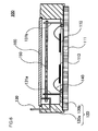
Fig. 1 is a sectional view of a semiconductor device according to a working example of the invention. -
Fig. 2 is a manufacturing flow diagram of the semiconductor device according to the working example of the invention. -
Fig. 3 is a plan view of the semiconductor device according to the working example of the invention at a manufacturing stage. -
Fig. 4 is a sectional view of the semiconductor device according to the working example of the invention at the manufacturing stage. -
Fig. 5A and 5B are a plan view and sectional view of control terminal insertion holes according to the working example of the invention. -
Fig. 6 is a sectional view of a semiconductor device according to a heretofore known example of the invention. -
Fig. 7 is a plan view of the semiconductor device according to the heretofore known example of the invention at a manufacturing stage. -
Fig. 8 is a sectional view of the semiconductor device according to the heretofore known example of the invention at the manufacturing stage. - Hereafter, a description will be given, based on the drawings, of a preferred embodiment (working example) of the invention.
- The same components will be given the same reference signs throughout the embodiment, and a redundant description will be omitted.
- The working example, not being limited to the described embodiment, can be changed into various forms without departing from the scope of the technical idea shown in the claims.
-
Fig. 1 is a sectional view of anIPM 1 which is a semiconductor device according to the working example of the invention. A description will be given hereafter of a configuration of the device. - An
insulating circuit substrate 12 is placed on ametal base plate 11 configured from a high thermal conductive metal such as copper or aluminum. Herein, theinsulating circuit substrate 12 is configured so that a metal thin film made of copper or the like is bonded to the lower surface of an insulating plate formed from insulating and high thermal conductive ceramics, such as alumina or silicone nitride, or the like, and a metal thin film, made of copper, on which is provided an electric circuit pattern for a main circuit is bonded to the upper surface of the insulating plate. The insulatingcircuit substrate 12 is also called a direct copper bonding (DCB) substrate or a metal insulating substrate. -
Power semiconductor elements 13, such as IGBTs, power MOSFETs, or FWDs, are placed on the electric circuit pattern thin film of the insulatingcircuit substrate 12. - Also, a
resin case 20 molded integrally withmetal connecting terminals metal base plate 11 so that the insulatingcircuit substrate 12 is surrounded by a casebottom portion 20b. The insulatingcircuit substrate 12 and casebottom portion 20b, as both of them are placed on themetal base plate 11, are disposed on substantially the same level. - The
power semiconductor elements 13 are each furnished with main circuit wiring and control wiring using bonding wires, lead frames, or the like, and are connected to a printedsubstrate 50 usingbonding wires 40 and the connectingterminals - As shown in
Fig. 1 , the printedsubstrate 50 is disposed on a level different from that of the insulatingcircuit substrate 12 and casebottom portion 20b, that is, they have a tiered structure. This is because it is possible to reduce the area used exclusively by the IPM as compared with when the printedsubstrate 50 is disposed on the same level as that of the insulatingcircuit substrate 12. - Control semiconductor elements and passive elements (not shown) are fixed to a surface of the printed
substrate 50, and these parts are connected by electric wiring. Also, in order to enable the electrical connection between the electric wiring and various kinds of terminals, through holes whose inner walls are subjected to a conductive treatment are provided in portions corresponding to the various kinds of terminals. - The control wiring between the printed
substrate 50 and the exterior of theIPM 1 is carried out using linearly shapedcontrol terminals 30. Thecontrol terminals 30 are held by being inserted in control terminal insertion holes 32 provided in thebottom portion 20b of thecase 20 and the through holes of the printedsubstrate 50. - Furthermore, the inner portion of the
IPM 1 is sealed with an insulating gel (not shown) or the like, and acover 60 for foreign material exclusion or the like is placed on the upper portion of theIPM 1. - The structure in which the linearly shaped
control terminals 30 are caused to stand upright by being inserted in the control terminal insertion holes 32 provided in the casebottom portion 20b and the through holes of the printedsubstrate 50 in this way is adopted, thereby eliminating the need for the resin thickness of acase sidewall 20a enough to hold the insert molded control terminals, thus enabling a reduction in the thickness of thecase sidewall 20a. Also, as horizontal extension wiring for connecting the control terminals and printed substrate, which has been needed in a heretofore known structure, is also no longer necessary, it is also no longer necessary to secure a space for the extension wiring. Because of these, it is possible to reduce the area used exclusively by the IPM as compared with in the heretofore known structure. - It is more effective to cause the
control terminals 30 to stand vertically from the casebottom portion 20b because it is thereby possible to minimize the area used exclusively by theIPM 1 as compared with when the control terminals are caused to stand on a slant or formed into a bent shape. - Subsequently, a description will be given of a method of manufacturing the
IPM 1.Fig. 2 is a manufacturing flow diagram of theIPM 1 according to the working example of the invention. Details will be described hereafter. - Firstly, the
power semiconductor elements 13 are mounted on the electric circuit pattern thin film of the insulatingcircuit substrate 12 by soldering or the like. The reason for using soldering here is to secure the electrical connection between thepower semiconductor elements 13 and the electric circuit pattern thin film of the insulatingcircuit substrate 12. - Furthermore, the insulating
circuit substrate 12 on which are mounted thepower semiconductor elements 13 is mounted on themetal base plate 11 by soldering or the like. The reason for using soldering here is to effectively release heat, generated from thepower semiconductor elements 13 when the IPM operates, to themetal base plate 11. - Meanwhile, the connecting
terminals case 20. The control terminal insertion holes 32 are also molded in the casebottom portion 20b simultaneously with the insert molding. - The molded
case 20 is mounted in a position on themetal base plate 11, in which the casebottom portion 20b surrounds the insulatingcircuit substrate 12, using an adhesive or the like. - In this condition, the connecting
terminals power semiconductor elements 13 are connected by thebonding wires 40 configured from aluminum, copper, or the like. Furthermore, the linearly shapedmetal control terminals 30 are mounted by being press fitted into the control terminal insertion holes 32 in predetermined positions. A plan view at this stage is shown inFig. 3 , and a sectional view along the line IV-IV' ofFig. 3 is shown inFig. 4 . - As shown in
Fig. 3 , the connectingterminals case 20. Also, a large number of the control terminal insertion holes 32 are in advance prepared at equal pitches on one side, and thecontrol terminals 30 are mounted in holes, of the control terminal insertion holes 32, corresponding to positions on the IPM appropriate to their respective use applications. - Subsequently, the printed
substrate 50 is mounted so that thecontrol terminals 30 and connectingterminals substrate 50. Furthermore, by, for example, soldering the connections of the through holes and their respective terminals, the electrical connection between the printedsubstrate 50 and each terminal is secured, and the printedsubstrate 50 is fixed in theIPM 1. - Finally, the insulating gel (not shown) is injected into the inner portion, and the
cover 60 is mounted, thereby completing theIPM 1. In the same way as in the previously described heretofore known technology, with regard to the main circuit wiring of theIPM 1 too, various kinds of wires are furnished with so as to be led out to the exterior, but an illustration and description are omitted here. - By enabling the mounting by preparing in advance the large number of control terminal insertion holes 32 at equal pitches, and press fitting the
control terminals 30 into the holes corresponding to their respective necessary positions on the IPM, in this way, it is possible to optionally set the combination of the terminal pitches and dispositions of thecontrol terminals 30. Because of this, there is an advantage that it is no longer necessary to prepare various kinds of case molding tools depending on a large number of uses, and that the degree of freedom of mounting the IPM on an external device also increases. - Also, when attempting to mount the control terminals on the insulating circuit substrate, the printed substrate, or the surface of the metal base plate, it is necessary to fix the end portions of the control terminals using a solder or adhesive, but in the invention, as the technique of fixing the end portions by press fitting the control terminals into the control terminal insertion holes is employed, man-hours decrease as compared with when using a solder or adhesive, meaning that it is also possible to obtain a cost reduction effect.
- Subsequently, a description will be given of the shape of the control terminal insertion holes 32.
Figs. 5A and 5B are each a plan view and sectional view of the controlterminal insertion hole 32 according to the working example of the invention. -
Fig. 5A shows a circular cylindrically shaped hole. It is effective to form the insertion holes 32 into a circular cylindrical shape or the like because it is thereby possible to easily carry out resin molding. It is necessary to make the diameter of the insertion holes 32 equal to or smaller than the diameter of thecontrol terminals 30.Fig. 5B shows a quadratic cylindrically shaped insertion hole. It is effective to employ the quadraticcylindrical control terminals 30 because the area of contact with the inner surfaces of the holes increases, as a result of which it is possible to strengthen a holding force even using only press fitting. - It is effective to configure each control
terminal insertion hole 32 into a cylindrical protruding portion such as protrudes from the surface of the casebottom portion 20b and covers the end portion of thecontrol terminal 30, as shown inFigs. 5A and 5B , because it is thereby easy for the control terminal insertion holes 32 to change in shape as compared with when simply providing holes in the surface of the casebottom portion 20b, and thus easy to press fit thecontrol terminals 30 even when variation occurs in the diameters of thecontrol terminals 30. Furthermore, the control terminal insertion holes 32 need a depth equal to or greater than a certain depth in order to enable thecontrol terminals 30 to be held even by only being press fitted, but it is possible to reduce the thickness of the casebottom portion 20b as compare with when simply providing holes in the casebottom portion 20b. Because of this, it is possible to reduce members necessary for molding thecase 20, and thus possible to contribute to a reduction in manufacturing cost. - The control terminal insertion holes 32 are configured so that the end portions of the
control terminals 30 are mounted by only being press fitted, but it is also possible to mount the end portions by adding an adhesive or the like. In this case, it is possible to further strengthen the holding force as compared with when the end portions are only press fitted, which is effective in improving the long-term reliability of the IPM. - Features, components and specific details of the structures of the above-described embodiments may be exchanged or combined to form further embodiments optimized for the respective application. As far as those modifications are readily apparent for an expert skilled in the art they shall be disclosed implicitly by the above description without specifying explicitly every possible combination, for the sake of conciseness of the present description.
Claims (5)
- A semiconductor device, comprising:power semiconductor elements;an insulating circuit substrate (12) on which the power semiconductor elements (13) are placed;a printed substrate (50), electrically connected to the power semiconductor elements (13), which has a control circuit;a case (20) having control terminal insertion holes (32) in the bottom portion (20b) thereof; andcontrol terminals (30) which electrically connect the printed substrate (50) and the exterior of the semiconductor device, whereinthe printed substrate (50) has a tiered structure with the insulating circuit substrate (12) and case bottom portion (20b), andthe control terminals (30), having a linear shape, are inserted in the control terminal insertion holes (32) and the through holes of the printed substrate (50).
- The semiconductor device according to claim 1, wherein
the number of control terminal insertion holes (32) is larger than the number of control terminals (30). - The semiconductor device according to claim 1 or 2, wherein
the control terminals (30) stand vertically from the case bottom portion (20b). - The semiconductor device according to at least one of claims 1 to 3, wherein
the control terminal insertion holes (32) are configured so as to protrude from the surface of the case bottom portion (20b) and enclose one end of each control terminal (30). - The semiconductor device according to at least one of claims 1 to 4, wherein
the insertion openings of the control terminal insertion holes (32) have a circular cylindrical structure or a quadratic cylindrical structure.
Applications Claiming Priority (1)
| Application Number | Priority Date | Filing Date | Title |
|---|---|---|---|
| JP2013046277A JP6119313B2 (en) | 2013-03-08 | 2013-03-08 | Semiconductor device |
Publications (2)
| Publication Number | Publication Date |
|---|---|
| EP2775524A1 true EP2775524A1 (en) | 2014-09-10 |
| EP2775524B1 EP2775524B1 (en) | 2022-05-11 |
Family
ID=49958381
Family Applications (1)
| Application Number | Title | Priority Date | Filing Date |
|---|---|---|---|
| EP14152231.8A Active EP2775524B1 (en) | 2013-03-08 | 2014-01-23 | Method for manufacturing a semiconductor device |
Country Status (4)
| Country | Link |
|---|---|
| US (1) | US9750137B2 (en) |
| EP (1) | EP2775524B1 (en) |
| JP (1) | JP6119313B2 (en) |
| CN (1) | CN104037147A (en) |
Cited By (1)
| Publication number | Priority date | Publication date | Assignee | Title |
|---|---|---|---|---|
| DE102017206195B4 (en) * | 2016-04-19 | 2020-11-26 | Mitsubishi Electric Corporation | Semiconductor device |
Families Citing this family (13)
| Publication number | Priority date | Publication date | Assignee | Title |
|---|---|---|---|---|
| SG10201504274SA (en) * | 2015-05-29 | 2016-12-29 | Delta Electronics Int’L Singapore Pte Ltd | Package assembly |
| JP2017028174A (en) * | 2015-07-24 | 2017-02-02 | サンケン電気株式会社 | Semiconductor device |
| JP6682824B2 (en) * | 2015-11-25 | 2020-04-15 | 富士電機株式会社 | Semiconductor device |
| EP3413348B1 (en) * | 2016-02-03 | 2021-05-26 | Shindengen Electric Manufacturing Co., Ltd. | Semiconductor device and method for manufacturing semiconductor device |
| JP6825306B2 (en) * | 2016-11-02 | 2021-02-03 | 富士電機株式会社 | Semiconductor device |
| CN110178219B (en) * | 2017-01-17 | 2022-11-22 | 三菱电机株式会社 | Semiconductor device and power conversion device |
| JP6981033B2 (en) * | 2017-04-19 | 2021-12-15 | 富士電機株式会社 | Semiconductor devices and methods for manufacturing semiconductor devices |
| JP6764389B2 (en) * | 2017-10-12 | 2020-09-30 | 矢崎総業株式会社 | Semiconductor module unit |
| CN108809056B (en) * | 2018-06-15 | 2019-11-19 | 西安微电子技术研究所 | A three-dimensional integrated intelligent power module and its manufacturing method |
| FR3084557B1 (en) * | 2018-07-30 | 2020-07-31 | Safran Electrical & Power | ELECTRICAL CONTROL DEVICE |
| JP7224272B2 (en) * | 2019-10-30 | 2023-02-17 | 三菱電機株式会社 | power semiconductor equipment |
| JP7577955B2 (en) * | 2020-09-25 | 2024-11-06 | 富士電機株式会社 | Semiconductor Device |
| CN116075080A (en) * | 2021-11-04 | 2023-05-05 | 光宝科技新加坡私人有限公司 | power module |
Citations (6)
| Publication number | Priority date | Publication date | Assignee | Title |
|---|---|---|---|---|
| JPH08204120A (en) * | 1995-01-20 | 1996-08-09 | Sansha Electric Mfg Co Ltd | Power semiconductor module |
| JPH1168035A (en) | 1997-06-12 | 1999-03-09 | Hitachi Ltd | Power semiconductor module |
| JP2000068446A (en) | 1998-08-25 | 2000-03-03 | Hitachi Ltd | Power semiconductor module |
| US6421244B1 (en) * | 1999-12-28 | 2002-07-16 | Mitsubishi Denki Kabushiki Kaisha | Power module |
| US20070284947A1 (en) * | 2006-04-20 | 2007-12-13 | Fairchild Korea Semiconductor, Ltd. | Power system module and method of fabricating the same |
| US20090096081A1 (en) * | 2007-10-15 | 2009-04-16 | Fuji Electric Device Technology Co., Ltd. | Semiconductor device |
Family Cites Families (17)
| Publication number | Priority date | Publication date | Assignee | Title |
|---|---|---|---|---|
| JP2936855B2 (en) * | 1991-12-26 | 1999-08-23 | 富士電機株式会社 | Power semiconductor device |
| EP0884781A3 (en) * | 1997-06-12 | 1999-06-30 | Hitachi, Ltd. | Power semiconductor module |
| JP3547333B2 (en) * | 1999-02-22 | 2004-07-28 | 株式会社日立産機システム | Power converter |
| JP4218193B2 (en) * | 2000-08-24 | 2009-02-04 | 三菱電機株式会社 | Power module |
| JP4151209B2 (en) * | 2000-08-29 | 2008-09-17 | 三菱電機株式会社 | Power semiconductor device |
| JPWO2002082542A1 (en) * | 2001-04-02 | 2004-07-29 | 三菱電機株式会社 | Power semiconductor devices |
| JP4129717B2 (en) * | 2001-05-30 | 2008-08-06 | 株式会社ルネサステクノロジ | Semiconductor device |
| DE10232566B4 (en) * | 2001-07-23 | 2015-11-12 | Fuji Electric Co., Ltd. | Semiconductor device |
| JP3845333B2 (en) * | 2002-04-30 | 2006-11-15 | 三菱電機株式会社 | Semiconductor power module |
| JP4886355B2 (en) * | 2006-05-02 | 2012-02-29 | 日本トムソン株式会社 | Slide device with built-in movable magnet type linear motor |
| TWI402952B (en) * | 2007-09-27 | 2013-07-21 | 三洋電機股份有限公司 | Circuit device and method of manufacturing same |
| US7944033B2 (en) * | 2007-10-18 | 2011-05-17 | Infineon Technologies Ag | Power semiconductor module |
| KR20090108954A (en) * | 2008-04-14 | 2009-10-19 | 삼성전자주식회사 | Semiconductor package and manufacturing method thereof |
| CN102439720B (en) | 2009-06-25 | 2014-08-27 | 富士电机株式会社 | Semiconductor device |
| CN102576706B (en) * | 2010-03-16 | 2015-07-22 | 富士电机株式会社 | Semiconductor device |
| JP5691475B2 (en) * | 2010-12-15 | 2015-04-01 | 富士電機株式会社 | Semiconductor device and manufacturing method thereof |
| JP6501606B2 (en) * | 2015-05-19 | 2019-04-17 | ルネサスエレクトロニクス株式会社 | Semiconductor device |
-
2013
- 2013-03-08 JP JP2013046277A patent/JP6119313B2/en not_active Expired - Fee Related
-
2014
- 2014-01-23 EP EP14152231.8A patent/EP2775524B1/en active Active
- 2014-02-12 CN CN201410049108.XA patent/CN104037147A/en active Pending
- 2014-02-14 US US14/181,503 patent/US9750137B2/en not_active Expired - Fee Related
Patent Citations (6)
| Publication number | Priority date | Publication date | Assignee | Title |
|---|---|---|---|---|
| JPH08204120A (en) * | 1995-01-20 | 1996-08-09 | Sansha Electric Mfg Co Ltd | Power semiconductor module |
| JPH1168035A (en) | 1997-06-12 | 1999-03-09 | Hitachi Ltd | Power semiconductor module |
| JP2000068446A (en) | 1998-08-25 | 2000-03-03 | Hitachi Ltd | Power semiconductor module |
| US6421244B1 (en) * | 1999-12-28 | 2002-07-16 | Mitsubishi Denki Kabushiki Kaisha | Power module |
| US20070284947A1 (en) * | 2006-04-20 | 2007-12-13 | Fairchild Korea Semiconductor, Ltd. | Power system module and method of fabricating the same |
| US20090096081A1 (en) * | 2007-10-15 | 2009-04-16 | Fuji Electric Device Technology Co., Ltd. | Semiconductor device |
Cited By (1)
| Publication number | Priority date | Publication date | Assignee | Title |
|---|---|---|---|---|
| DE102017206195B4 (en) * | 2016-04-19 | 2020-11-26 | Mitsubishi Electric Corporation | Semiconductor device |
Also Published As
| Publication number | Publication date |
|---|---|
| JP2014175444A (en) | 2014-09-22 |
| US9750137B2 (en) | 2017-08-29 |
| JP6119313B2 (en) | 2017-04-26 |
| EP2775524B1 (en) | 2022-05-11 |
| CN104037147A (en) | 2014-09-10 |
| US20140254116A1 (en) | 2014-09-11 |
Similar Documents
| Publication | Publication Date | Title |
|---|---|---|
| EP2775524B1 (en) | Method for manufacturing a semiconductor device | |
| US8975740B2 (en) | Semiconductor module | |
| CN105612613B (en) | Semiconductor device | |
| EP3288075B1 (en) | Power semiconductor module | |
| US20140029201A1 (en) | Power package module and manufacturing method thereof | |
| US9735086B2 (en) | Power semiconductor module having a two-part housing | |
| WO2016031462A1 (en) | Power semiconductor module | |
| KR20070103876A (en) | Power system module and its manufacturing method | |
| CN103872036A (en) | Semiconductor module and method of manufacturing the same | |
| JP2016012604A (en) | Semiconductor device manufacturing method | |
| CN112750801A (en) | Power semiconductor device | |
| CN108538825A (en) | Power module | |
| JP2013171870A (en) | Semiconductor module and manufacturing method thereof | |
| CN103858228A (en) | Semiconductor device and method of manufacture thereof | |
| CN104600051B (en) | Semiconductor module | |
| JP2015023226A (en) | Wide gap semiconductor device | |
| US8471370B2 (en) | Semiconductor element with semiconductor die and lead frames | |
| CN101501843A (en) | Molded housing used in force fit method | |
| KR101983165B1 (en) | Semiconductor package | |
| US10653020B2 (en) | Electronic module and method for producing an electronic module | |
| JP2012074588A (en) | Semiconductor power module and method for manufacturing the same | |
| JP6769556B2 (en) | Semiconductor devices and semiconductor modules | |
| US12489095B2 (en) | Semiconductor apparatus | |
| EP4148789A1 (en) | Power semiconductor modules | |
| KR20140139649A (en) | Intergral terminal frame and power module having the same |
Legal Events
| Date | Code | Title | Description |
|---|---|---|---|
| PUAI | Public reference made under article 153(3) epc to a published international application that has entered the european phase |
Free format text: ORIGINAL CODE: 0009012 |
|
| 17P | Request for examination filed |
Effective date: 20140123 |
|
| AK | Designated contracting states |
Kind code of ref document: A1 Designated state(s): AL AT BE BG CH CY CZ DE DK EE ES FI FR GB GR HR HU IE IS IT LI LT LU LV MC MK MT NL NO PL PT RO RS SE SI SK SM TR |
|
| AX | Request for extension of the european patent |
Extension state: BA ME |
|
| R17P | Request for examination filed (corrected) |
Effective date: 20150310 |
|
| RBV | Designated contracting states (corrected) |
Designated state(s): AL AT BE BG CH CY CZ DE DK EE ES FI FR GB GR HR HU IE IS IT LI LT LU LV MC MK MT NL NO PL PT RO RS SE SI SK SM TR |
|
| STAA | Information on the status of an ep patent application or granted ep patent |
Free format text: STATUS: EXAMINATION IS IN PROGRESS |
|
| 17Q | First examination report despatched |
Effective date: 20190508 |
|
| GRAP | Despatch of communication of intention to grant a patent |
Free format text: ORIGINAL CODE: EPIDOSNIGR1 |
|
| STAA | Information on the status of an ep patent application or granted ep patent |
Free format text: STATUS: GRANT OF PATENT IS INTENDED |
|
| RIC1 | Information provided on ipc code assigned before grant |
Ipc: H01L 23/053 20060101ALI20211018BHEP Ipc: H01L 25/16 20060101AFI20211018BHEP |
|
| INTG | Intention to grant announced |
Effective date: 20211122 |
|
| GRAS | Grant fee paid |
Free format text: ORIGINAL CODE: EPIDOSNIGR3 |
|
| GRAA | (expected) grant |
Free format text: ORIGINAL CODE: 0009210 |
|
| STAA | Information on the status of an ep patent application or granted ep patent |
Free format text: STATUS: THE PATENT HAS BEEN GRANTED |
|
| AK | Designated contracting states |
Kind code of ref document: B1 Designated state(s): AL AT BE BG CH CY CZ DE DK EE ES FI FR GB GR HR HU IE IS IT LI LT LU LV MC MK MT NL NO PL PT RO RS SE SI SK SM TR |
|
| REG | Reference to a national code |
Ref country code: GB Ref legal event code: FG4D |
|
| REG | Reference to a national code |
Ref country code: CH Ref legal event code: EP |
|
| REG | Reference to a national code |
Ref country code: AT Ref legal event code: REF Ref document number: 1492193 Country of ref document: AT Kind code of ref document: T Effective date: 20220515 |
|
| REG | Reference to a national code |
Ref country code: DE Ref legal event code: R096 Ref document number: 602014083660 Country of ref document: DE |
|
| REG | Reference to a national code |
Ref country code: IE Ref legal event code: FG4D |
|
| REG | Reference to a national code |
Ref country code: LT Ref legal event code: MG9D |
|
| REG | Reference to a national code |
Ref country code: NL Ref legal event code: MP Effective date: 20220511 |
|
| REG | Reference to a national code |
Ref country code: AT Ref legal event code: MK05 Ref document number: 1492193 Country of ref document: AT Kind code of ref document: T Effective date: 20220511 |
|
| PG25 | Lapsed in a contracting state [announced via postgrant information from national office to epo] |
Ref country code: SE Free format text: LAPSE BECAUSE OF FAILURE TO SUBMIT A TRANSLATION OF THE DESCRIPTION OR TO PAY THE FEE WITHIN THE PRESCRIBED TIME-LIMIT Effective date: 20220511 Ref country code: PT Free format text: LAPSE BECAUSE OF FAILURE TO SUBMIT A TRANSLATION OF THE DESCRIPTION OR TO PAY THE FEE WITHIN THE PRESCRIBED TIME-LIMIT Effective date: 20220912 Ref country code: NO Free format text: LAPSE BECAUSE OF FAILURE TO SUBMIT A TRANSLATION OF THE DESCRIPTION OR TO PAY THE FEE WITHIN THE PRESCRIBED TIME-LIMIT Effective date: 20220811 Ref country code: NL Free format text: LAPSE BECAUSE OF FAILURE TO SUBMIT A TRANSLATION OF THE DESCRIPTION OR TO PAY THE FEE WITHIN THE PRESCRIBED TIME-LIMIT Effective date: 20220511 Ref country code: LT Free format text: LAPSE BECAUSE OF FAILURE TO SUBMIT A TRANSLATION OF THE DESCRIPTION OR TO PAY THE FEE WITHIN THE PRESCRIBED TIME-LIMIT Effective date: 20220511 Ref country code: HR Free format text: LAPSE BECAUSE OF FAILURE TO SUBMIT A TRANSLATION OF THE DESCRIPTION OR TO PAY THE FEE WITHIN THE PRESCRIBED TIME-LIMIT Effective date: 20220511 Ref country code: GR Free format text: LAPSE BECAUSE OF FAILURE TO SUBMIT A TRANSLATION OF THE DESCRIPTION OR TO PAY THE FEE WITHIN THE PRESCRIBED TIME-LIMIT Effective date: 20220812 Ref country code: FI Free format text: LAPSE BECAUSE OF FAILURE TO SUBMIT A TRANSLATION OF THE DESCRIPTION OR TO PAY THE FEE WITHIN THE PRESCRIBED TIME-LIMIT Effective date: 20220511 Ref country code: ES Free format text: LAPSE BECAUSE OF FAILURE TO SUBMIT A TRANSLATION OF THE DESCRIPTION OR TO PAY THE FEE WITHIN THE PRESCRIBED TIME-LIMIT Effective date: 20220511 Ref country code: BG Free format text: LAPSE BECAUSE OF FAILURE TO SUBMIT A TRANSLATION OF THE DESCRIPTION OR TO PAY THE FEE WITHIN THE PRESCRIBED TIME-LIMIT Effective date: 20220811 Ref country code: AT Free format text: LAPSE BECAUSE OF FAILURE TO SUBMIT A TRANSLATION OF THE DESCRIPTION OR TO PAY THE FEE WITHIN THE PRESCRIBED TIME-LIMIT Effective date: 20220511 |
|
| PG25 | Lapsed in a contracting state [announced via postgrant information from national office to epo] |
Ref country code: RS Free format text: LAPSE BECAUSE OF FAILURE TO SUBMIT A TRANSLATION OF THE DESCRIPTION OR TO PAY THE FEE WITHIN THE PRESCRIBED TIME-LIMIT Effective date: 20220511 Ref country code: PL Free format text: LAPSE BECAUSE OF FAILURE TO SUBMIT A TRANSLATION OF THE DESCRIPTION OR TO PAY THE FEE WITHIN THE PRESCRIBED TIME-LIMIT Effective date: 20220511 Ref country code: LV Free format text: LAPSE BECAUSE OF FAILURE TO SUBMIT A TRANSLATION OF THE DESCRIPTION OR TO PAY THE FEE WITHIN THE PRESCRIBED TIME-LIMIT Effective date: 20220511 Ref country code: IS Free format text: LAPSE BECAUSE OF FAILURE TO SUBMIT A TRANSLATION OF THE DESCRIPTION OR TO PAY THE FEE WITHIN THE PRESCRIBED TIME-LIMIT Effective date: 20220911 |
|
| PG25 | Lapsed in a contracting state [announced via postgrant information from national office to epo] |
Ref country code: SM Free format text: LAPSE BECAUSE OF FAILURE TO SUBMIT A TRANSLATION OF THE DESCRIPTION OR TO PAY THE FEE WITHIN THE PRESCRIBED TIME-LIMIT Effective date: 20220511 Ref country code: SK Free format text: LAPSE BECAUSE OF FAILURE TO SUBMIT A TRANSLATION OF THE DESCRIPTION OR TO PAY THE FEE WITHIN THE PRESCRIBED TIME-LIMIT Effective date: 20220511 Ref country code: RO Free format text: LAPSE BECAUSE OF FAILURE TO SUBMIT A TRANSLATION OF THE DESCRIPTION OR TO PAY THE FEE WITHIN THE PRESCRIBED TIME-LIMIT Effective date: 20220511 Ref country code: EE Free format text: LAPSE BECAUSE OF FAILURE TO SUBMIT A TRANSLATION OF THE DESCRIPTION OR TO PAY THE FEE WITHIN THE PRESCRIBED TIME-LIMIT Effective date: 20220511 Ref country code: DK Free format text: LAPSE BECAUSE OF FAILURE TO SUBMIT A TRANSLATION OF THE DESCRIPTION OR TO PAY THE FEE WITHIN THE PRESCRIBED TIME-LIMIT Effective date: 20220511 Ref country code: CZ Free format text: LAPSE BECAUSE OF FAILURE TO SUBMIT A TRANSLATION OF THE DESCRIPTION OR TO PAY THE FEE WITHIN THE PRESCRIBED TIME-LIMIT Effective date: 20220511 |
|
| REG | Reference to a national code |
Ref country code: DE Ref legal event code: R097 Ref document number: 602014083660 Country of ref document: DE |
|
| PLBE | No opposition filed within time limit |
Free format text: ORIGINAL CODE: 0009261 |
|
| STAA | Information on the status of an ep patent application or granted ep patent |
Free format text: STATUS: NO OPPOSITION FILED WITHIN TIME LIMIT |
|
| PG25 | Lapsed in a contracting state [announced via postgrant information from national office to epo] |
Ref country code: AL Free format text: LAPSE BECAUSE OF FAILURE TO SUBMIT A TRANSLATION OF THE DESCRIPTION OR TO PAY THE FEE WITHIN THE PRESCRIBED TIME-LIMIT Effective date: 20220511 |
|
| 26N | No opposition filed |
Effective date: 20230214 |
|
| PG25 | Lapsed in a contracting state [announced via postgrant information from national office to epo] |
Ref country code: SI Free format text: LAPSE BECAUSE OF FAILURE TO SUBMIT A TRANSLATION OF THE DESCRIPTION OR TO PAY THE FEE WITHIN THE PRESCRIBED TIME-LIMIT Effective date: 20220511 |
|
| PGFP | Annual fee paid to national office [announced via postgrant information from national office to epo] |
Ref country code: DE Payment date: 20230131 Year of fee payment: 10 |
|
| REG | Reference to a national code |
Ref country code: CH Ref legal event code: PL |
|
| GBPC | Gb: european patent ceased through non-payment of renewal fee |
Effective date: 20230123 |
|
| PG25 | Lapsed in a contracting state [announced via postgrant information from national office to epo] |
Ref country code: LU Free format text: LAPSE BECAUSE OF NON-PAYMENT OF DUE FEES Effective date: 20230123 |
|
| REG | Reference to a national code |
Ref country code: BE Ref legal event code: MM Effective date: 20230131 |
|
| PG25 | Lapsed in a contracting state [announced via postgrant information from national office to epo] |
Ref country code: LI Free format text: LAPSE BECAUSE OF NON-PAYMENT OF DUE FEES Effective date: 20230131 Ref country code: GB Free format text: LAPSE BECAUSE OF NON-PAYMENT OF DUE FEES Effective date: 20230123 Ref country code: CH Free format text: LAPSE BECAUSE OF NON-PAYMENT OF DUE FEES Effective date: 20230131 |
|
| PG25 | Lapsed in a contracting state [announced via postgrant information from national office to epo] |
Ref country code: FR Free format text: LAPSE BECAUSE OF NON-PAYMENT OF DUE FEES Effective date: 20230131 Ref country code: BE Free format text: LAPSE BECAUSE OF NON-PAYMENT OF DUE FEES Effective date: 20230131 |
|
| PG25 | Lapsed in a contracting state [announced via postgrant information from national office to epo] |
Ref country code: IT Free format text: LAPSE BECAUSE OF FAILURE TO SUBMIT A TRANSLATION OF THE DESCRIPTION OR TO PAY THE FEE WITHIN THE PRESCRIBED TIME-LIMIT Effective date: 20220511 Ref country code: IE Free format text: LAPSE BECAUSE OF NON-PAYMENT OF DUE FEES Effective date: 20230123 |
|
| PG25 | Lapsed in a contracting state [announced via postgrant information from national office to epo] |
Ref country code: MC Free format text: LAPSE BECAUSE OF FAILURE TO SUBMIT A TRANSLATION OF THE DESCRIPTION OR TO PAY THE FEE WITHIN THE PRESCRIBED TIME-LIMIT Effective date: 20220511 |
|
| PG25 | Lapsed in a contracting state [announced via postgrant information from national office to epo] |
Ref country code: MC Free format text: LAPSE BECAUSE OF FAILURE TO SUBMIT A TRANSLATION OF THE DESCRIPTION OR TO PAY THE FEE WITHIN THE PRESCRIBED TIME-LIMIT Effective date: 20220511 |
|
| REG | Reference to a national code |
Ref country code: DE Ref legal event code: R119 Ref document number: 602014083660 Country of ref document: DE |
|
| PG25 | Lapsed in a contracting state [announced via postgrant information from national office to epo] |
Ref country code: DE Free format text: LAPSE BECAUSE OF NON-PAYMENT OF DUE FEES Effective date: 20240801 |
|
| PG25 | Lapsed in a contracting state [announced via postgrant information from national office to epo] |
Ref country code: DE Free format text: LAPSE BECAUSE OF NON-PAYMENT OF DUE FEES Effective date: 20240801 |
|
| PG25 | Lapsed in a contracting state [announced via postgrant information from national office to epo] |
Ref country code: BG Free format text: LAPSE BECAUSE OF FAILURE TO SUBMIT A TRANSLATION OF THE DESCRIPTION OR TO PAY THE FEE WITHIN THE PRESCRIBED TIME-LIMIT Effective date: 20220511 |
|
| PG25 | Lapsed in a contracting state [announced via postgrant information from national office to epo] |
Ref country code: BG Free format text: LAPSE BECAUSE OF FAILURE TO SUBMIT A TRANSLATION OF THE DESCRIPTION OR TO PAY THE FEE WITHIN THE PRESCRIBED TIME-LIMIT Effective date: 20220511 |
|
| PG25 | Lapsed in a contracting state [announced via postgrant information from national office to epo] |
Ref country code: CY Free format text: LAPSE BECAUSE OF FAILURE TO SUBMIT A TRANSLATION OF THE DESCRIPTION OR TO PAY THE FEE WITHIN THE PRESCRIBED TIME-LIMIT; INVALID AB INITIO Effective date: 20140123 |
|
| PG25 | Lapsed in a contracting state [announced via postgrant information from national office to epo] |
Ref country code: HU Free format text: LAPSE BECAUSE OF FAILURE TO SUBMIT A TRANSLATION OF THE DESCRIPTION OR TO PAY THE FEE WITHIN THE PRESCRIBED TIME-LIMIT; INVALID AB INITIO Effective date: 20140123 |
|
| PG25 | Lapsed in a contracting state [announced via postgrant information from national office to epo] |
Ref country code: TR Free format text: LAPSE BECAUSE OF FAILURE TO SUBMIT A TRANSLATION OF THE DESCRIPTION OR TO PAY THE FEE WITHIN THE PRESCRIBED TIME-LIMIT Effective date: 20220511 |