EP2772936B1 - Method of wire bonding parallel bond wires aswell as a reshaping process of the same, and the related apparatus - Google Patents
Method of wire bonding parallel bond wires aswell as a reshaping process of the same, and the related apparatus Download PDFInfo
- Publication number
- EP2772936B1 EP2772936B1 EP14157235.4A EP14157235A EP2772936B1 EP 2772936 B1 EP2772936 B1 EP 2772936B1 EP 14157235 A EP14157235 A EP 14157235A EP 2772936 B1 EP2772936 B1 EP 2772936B1
- Authority
- EP
- European Patent Office
- Prior art keywords
- wires
- interconnection
- elements
- length
- interconnected
- Prior art date
- Legal status (The legal status is an assumption and is not a legal conclusion. Google has not performed a legal analysis and makes no representation as to the accuracy of the status listed.)
- Active
Links
- 238000000034 method Methods 0.000 title claims description 62
- 238000007493 shaping process Methods 0.000 claims description 25
- 239000011248 coating agent Substances 0.000 claims description 12
- 238000000576 coating method Methods 0.000 claims description 12
- 239000003989 dielectric material Substances 0.000 claims description 12
- 239000012212 insulator Substances 0.000 claims 2
- 239000000758 substrate Substances 0.000 description 8
- 230000005540 biological transmission Effects 0.000 description 7
- 238000004519 manufacturing process Methods 0.000 description 6
- 230000006978 adaptation Effects 0.000 description 5
- 238000004026 adhesive bonding Methods 0.000 description 4
- 238000009413 insulation Methods 0.000 description 4
- 238000005476 soldering Methods 0.000 description 4
- 238000007906 compression Methods 0.000 description 3
- 230000017525 heat dissipation Effects 0.000 description 3
- 230000000007 visual effect Effects 0.000 description 3
- 230000000712 assembly Effects 0.000 description 2
- 238000000429 assembly Methods 0.000 description 2
- 239000000463 material Substances 0.000 description 2
- 239000011159 matrix material Substances 0.000 description 2
- 239000011325 microbead Substances 0.000 description 2
- 230000003071 parasitic effect Effects 0.000 description 2
- 239000004020 conductor Substances 0.000 description 1
- 230000008878 coupling Effects 0.000 description 1
- 238000010168 coupling process Methods 0.000 description 1
- 238000005859 coupling reaction Methods 0.000 description 1
- 238000002788 crimping Methods 0.000 description 1
- 239000012777 electrically insulating material Substances 0.000 description 1
- 238000009434 installation Methods 0.000 description 1
- 239000011810 insulating material Substances 0.000 description 1
- 230000035939 shock Effects 0.000 description 1
- 238000003466 welding Methods 0.000 description 1
Images


Classifications
-
- H—ELECTRICITY
- H01—ELECTRIC ELEMENTS
- H01L—SEMICONDUCTOR DEVICES NOT COVERED BY CLASS H10
- H01L24/00—Arrangements for connecting or disconnecting semiconductor or solid-state bodies; Methods or apparatus related thereto
- H01L24/01—Means for bonding being attached to, or being formed on, the surface to be connected, e.g. chip-to-package, die-attach, "first-level" interconnects; Manufacturing methods related thereto
- H01L24/42—Wire connectors; Manufacturing methods related thereto
- H01L24/47—Structure, shape, material or disposition of the wire connectors after the connecting process
- H01L24/48—Structure, shape, material or disposition of the wire connectors after the connecting process of an individual wire connector
-
- H—ELECTRICITY
- H01—ELECTRIC ELEMENTS
- H01L—SEMICONDUCTOR DEVICES NOT COVERED BY CLASS H10
- H01L23/00—Details of semiconductor or other solid state devices
- H01L23/58—Structural electrical arrangements for semiconductor devices not otherwise provided for, e.g. in combination with batteries
- H01L23/64—Impedance arrangements
- H01L23/66—High-frequency adaptations
-
- H—ELECTRICITY
- H01—ELECTRIC ELEMENTS
- H01L—SEMICONDUCTOR DEVICES NOT COVERED BY CLASS H10
- H01L24/00—Arrangements for connecting or disconnecting semiconductor or solid-state bodies; Methods or apparatus related thereto
- H01L24/01—Means for bonding being attached to, or being formed on, the surface to be connected, e.g. chip-to-package, die-attach, "first-level" interconnects; Manufacturing methods related thereto
- H01L24/42—Wire connectors; Manufacturing methods related thereto
- H01L24/47—Structure, shape, material or disposition of the wire connectors after the connecting process
- H01L24/49—Structure, shape, material or disposition of the wire connectors after the connecting process of a plurality of wire connectors
-
- H—ELECTRICITY
- H01—ELECTRIC ELEMENTS
- H01L—SEMICONDUCTOR DEVICES NOT COVERED BY CLASS H10
- H01L24/00—Arrangements for connecting or disconnecting semiconductor or solid-state bodies; Methods or apparatus related thereto
- H01L24/74—Apparatus for manufacturing arrangements for connecting or disconnecting semiconductor or solid-state bodies
- H01L24/78—Apparatus for connecting with wire connectors
-
- H—ELECTRICITY
- H01—ELECTRIC ELEMENTS
- H01L—SEMICONDUCTOR DEVICES NOT COVERED BY CLASS H10
- H01L24/00—Arrangements for connecting or disconnecting semiconductor or solid-state bodies; Methods or apparatus related thereto
- H01L24/80—Methods for connecting semiconductor or other solid state bodies using means for bonding being attached to, or being formed on, the surface to be connected
- H01L24/85—Methods for connecting semiconductor or other solid state bodies using means for bonding being attached to, or being formed on, the surface to be connected using a wire connector
-
- H—ELECTRICITY
- H01—ELECTRIC ELEMENTS
- H01L—SEMICONDUCTOR DEVICES NOT COVERED BY CLASS H10
- H01L2223/00—Details relating to semiconductor or other solid state devices covered by the group H01L23/00
- H01L2223/58—Structural electrical arrangements for semiconductor devices not otherwise provided for
- H01L2223/64—Impedance arrangements
- H01L2223/66—High-frequency adaptations
- H01L2223/6605—High-frequency electrical connections
- H01L2223/6611—Wire connections
-
- H—ELECTRICITY
- H01—ELECTRIC ELEMENTS
- H01L—SEMICONDUCTOR DEVICES NOT COVERED BY CLASS H10
- H01L2224/00—Indexing scheme for arrangements for connecting or disconnecting semiconductor or solid-state bodies and methods related thereto as covered by H01L24/00
- H01L2224/01—Means for bonding being attached to, or being formed on, the surface to be connected, e.g. chip-to-package, die-attach, "first-level" interconnects; Manufacturing methods related thereto
- H01L2224/02—Bonding areas; Manufacturing methods related thereto
- H01L2224/04—Structure, shape, material or disposition of the bonding areas prior to the connecting process
- H01L2224/05—Structure, shape, material or disposition of the bonding areas prior to the connecting process of an individual bonding area
- H01L2224/0554—External layer
- H01L2224/0555—Shape
- H01L2224/05552—Shape in top view
- H01L2224/05554—Shape in top view being square
-
- H—ELECTRICITY
- H01—ELECTRIC ELEMENTS
- H01L—SEMICONDUCTOR DEVICES NOT COVERED BY CLASS H10
- H01L2224/00—Indexing scheme for arrangements for connecting or disconnecting semiconductor or solid-state bodies and methods related thereto as covered by H01L24/00
- H01L2224/01—Means for bonding being attached to, or being formed on, the surface to be connected, e.g. chip-to-package, die-attach, "first-level" interconnects; Manufacturing methods related thereto
- H01L2224/42—Wire connectors; Manufacturing methods related thereto
- H01L2224/44—Structure, shape, material or disposition of the wire connectors prior to the connecting process
- H01L2224/45—Structure, shape, material or disposition of the wire connectors prior to the connecting process of an individual wire connector
- H01L2224/45001—Core members of the connector
- H01L2224/4501—Shape
- H01L2224/45012—Cross-sectional shape
- H01L2224/45014—Ribbon connectors, e.g. rectangular cross-section
-
- H—ELECTRICITY
- H01—ELECTRIC ELEMENTS
- H01L—SEMICONDUCTOR DEVICES NOT COVERED BY CLASS H10
- H01L2224/00—Indexing scheme for arrangements for connecting or disconnecting semiconductor or solid-state bodies and methods related thereto as covered by H01L24/00
- H01L2224/01—Means for bonding being attached to, or being formed on, the surface to be connected, e.g. chip-to-package, die-attach, "first-level" interconnects; Manufacturing methods related thereto
- H01L2224/42—Wire connectors; Manufacturing methods related thereto
- H01L2224/44—Structure, shape, material or disposition of the wire connectors prior to the connecting process
- H01L2224/45—Structure, shape, material or disposition of the wire connectors prior to the connecting process of an individual wire connector
- H01L2224/4554—Coating
- H01L2224/45565—Single coating layer
-
- H—ELECTRICITY
- H01—ELECTRIC ELEMENTS
- H01L—SEMICONDUCTOR DEVICES NOT COVERED BY CLASS H10
- H01L2224/00—Indexing scheme for arrangements for connecting or disconnecting semiconductor or solid-state bodies and methods related thereto as covered by H01L24/00
- H01L2224/01—Means for bonding being attached to, or being formed on, the surface to be connected, e.g. chip-to-package, die-attach, "first-level" interconnects; Manufacturing methods related thereto
- H01L2224/42—Wire connectors; Manufacturing methods related thereto
- H01L2224/47—Structure, shape, material or disposition of the wire connectors after the connecting process
- H01L2224/48—Structure, shape, material or disposition of the wire connectors after the connecting process of an individual wire connector
- H01L2224/4801—Structure
- H01L2224/48011—Length
-
- H—ELECTRICITY
- H01—ELECTRIC ELEMENTS
- H01L—SEMICONDUCTOR DEVICES NOT COVERED BY CLASS H10
- H01L2224/00—Indexing scheme for arrangements for connecting or disconnecting semiconductor or solid-state bodies and methods related thereto as covered by H01L24/00
- H01L2224/01—Means for bonding being attached to, or being formed on, the surface to be connected, e.g. chip-to-package, die-attach, "first-level" interconnects; Manufacturing methods related thereto
- H01L2224/42—Wire connectors; Manufacturing methods related thereto
- H01L2224/47—Structure, shape, material or disposition of the wire connectors after the connecting process
- H01L2224/48—Structure, shape, material or disposition of the wire connectors after the connecting process of an individual wire connector
- H01L2224/481—Disposition
- H01L2224/48105—Connecting bonding areas at different heights
-
- H—ELECTRICITY
- H01—ELECTRIC ELEMENTS
- H01L—SEMICONDUCTOR DEVICES NOT COVERED BY CLASS H10
- H01L2224/00—Indexing scheme for arrangements for connecting or disconnecting semiconductor or solid-state bodies and methods related thereto as covered by H01L24/00
- H01L2224/01—Means for bonding being attached to, or being formed on, the surface to be connected, e.g. chip-to-package, die-attach, "first-level" interconnects; Manufacturing methods related thereto
- H01L2224/42—Wire connectors; Manufacturing methods related thereto
- H01L2224/47—Structure, shape, material or disposition of the wire connectors after the connecting process
- H01L2224/48—Structure, shape, material or disposition of the wire connectors after the connecting process of an individual wire connector
- H01L2224/481—Disposition
- H01L2224/48135—Connecting between different semiconductor or solid-state bodies, i.e. chip-to-chip
- H01L2224/48137—Connecting between different semiconductor or solid-state bodies, i.e. chip-to-chip the bodies being arranged next to each other, e.g. on a common substrate
-
- H—ELECTRICITY
- H01—ELECTRIC ELEMENTS
- H01L—SEMICONDUCTOR DEVICES NOT COVERED BY CLASS H10
- H01L2224/00—Indexing scheme for arrangements for connecting or disconnecting semiconductor or solid-state bodies and methods related thereto as covered by H01L24/00
- H01L2224/01—Means for bonding being attached to, or being formed on, the surface to be connected, e.g. chip-to-package, die-attach, "first-level" interconnects; Manufacturing methods related thereto
- H01L2224/42—Wire connectors; Manufacturing methods related thereto
- H01L2224/47—Structure, shape, material or disposition of the wire connectors after the connecting process
- H01L2224/48—Structure, shape, material or disposition of the wire connectors after the connecting process of an individual wire connector
- H01L2224/4899—Auxiliary members for wire connectors, e.g. flow-barriers, reinforcing structures, spacers, alignment aids
- H01L2224/48996—Auxiliary members for wire connectors, e.g. flow-barriers, reinforcing structures, spacers, alignment aids being formed on an item to be connected not being a semiconductor or solid-state body
-
- H—ELECTRICITY
- H01—ELECTRIC ELEMENTS
- H01L—SEMICONDUCTOR DEVICES NOT COVERED BY CLASS H10
- H01L2224/00—Indexing scheme for arrangements for connecting or disconnecting semiconductor or solid-state bodies and methods related thereto as covered by H01L24/00
- H01L2224/01—Means for bonding being attached to, or being formed on, the surface to be connected, e.g. chip-to-package, die-attach, "first-level" interconnects; Manufacturing methods related thereto
- H01L2224/42—Wire connectors; Manufacturing methods related thereto
- H01L2224/47—Structure, shape, material or disposition of the wire connectors after the connecting process
- H01L2224/49—Structure, shape, material or disposition of the wire connectors after the connecting process of a plurality of wire connectors
- H01L2224/4905—Shape
- H01L2224/4909—Loop shape arrangement
- H01L2224/49095—Loop shape arrangement parallel in plane
- H01L2224/49096—Loop shape arrangement parallel in plane horizontal
-
- H—ELECTRICITY
- H01—ELECTRIC ELEMENTS
- H01L—SEMICONDUCTOR DEVICES NOT COVERED BY CLASS H10
- H01L2224/00—Indexing scheme for arrangements for connecting or disconnecting semiconductor or solid-state bodies and methods related thereto as covered by H01L24/00
- H01L2224/01—Means for bonding being attached to, or being formed on, the surface to be connected, e.g. chip-to-package, die-attach, "first-level" interconnects; Manufacturing methods related thereto
- H01L2224/42—Wire connectors; Manufacturing methods related thereto
- H01L2224/47—Structure, shape, material or disposition of the wire connectors after the connecting process
- H01L2224/49—Structure, shape, material or disposition of the wire connectors after the connecting process of a plurality of wire connectors
- H01L2224/491—Disposition
- H01L2224/4912—Layout
- H01L2224/4917—Crossed wires
-
- H—ELECTRICITY
- H01—ELECTRIC ELEMENTS
- H01L—SEMICONDUCTOR DEVICES NOT COVERED BY CLASS H10
- H01L2224/00—Indexing scheme for arrangements for connecting or disconnecting semiconductor or solid-state bodies and methods related thereto as covered by H01L24/00
- H01L2224/01—Means for bonding being attached to, or being formed on, the surface to be connected, e.g. chip-to-package, die-attach, "first-level" interconnects; Manufacturing methods related thereto
- H01L2224/42—Wire connectors; Manufacturing methods related thereto
- H01L2224/47—Structure, shape, material or disposition of the wire connectors after the connecting process
- H01L2224/49—Structure, shape, material or disposition of the wire connectors after the connecting process of a plurality of wire connectors
- H01L2224/491—Disposition
- H01L2224/4912—Layout
- H01L2224/49175—Parallel arrangements
-
- H—ELECTRICITY
- H01—ELECTRIC ELEMENTS
- H01L—SEMICONDUCTOR DEVICES NOT COVERED BY CLASS H10
- H01L2224/00—Indexing scheme for arrangements for connecting or disconnecting semiconductor or solid-state bodies and methods related thereto as covered by H01L24/00
- H01L2224/74—Apparatus for manufacturing arrangements for connecting or disconnecting semiconductor or solid-state bodies and for methods related thereto
- H01L2224/78—Apparatus for connecting with wire connectors
- H01L2224/7855—Mechanical means, e.g. for severing, pressing, stamping
-
- H—ELECTRICITY
- H01—ELECTRIC ELEMENTS
- H01L—SEMICONDUCTOR DEVICES NOT COVERED BY CLASS H10
- H01L2224/00—Indexing scheme for arrangements for connecting or disconnecting semiconductor or solid-state bodies and methods related thereto as covered by H01L24/00
- H01L2224/80—Methods for connecting semiconductor or other solid state bodies using means for bonding being attached to, or being formed on, the surface to be connected
- H01L2224/85—Methods for connecting semiconductor or other solid state bodies using means for bonding being attached to, or being formed on, the surface to be connected using a wire connector
- H01L2224/852—Applying energy for connecting
- H01L2224/85201—Compression bonding
- H01L2224/85203—Thermocompression bonding
-
- H—ELECTRICITY
- H01—ELECTRIC ELEMENTS
- H01L—SEMICONDUCTOR DEVICES NOT COVERED BY CLASS H10
- H01L2224/00—Indexing scheme for arrangements for connecting or disconnecting semiconductor or solid-state bodies and methods related thereto as covered by H01L24/00
- H01L2224/80—Methods for connecting semiconductor or other solid state bodies using means for bonding being attached to, or being formed on, the surface to be connected
- H01L2224/85—Methods for connecting semiconductor or other solid state bodies using means for bonding being attached to, or being formed on, the surface to be connected using a wire connector
- H01L2224/852—Applying energy for connecting
- H01L2224/85201—Compression bonding
- H01L2224/85205—Ultrasonic bonding
- H01L2224/85207—Thermosonic bonding
-
- H—ELECTRICITY
- H01—ELECTRIC ELEMENTS
- H01L—SEMICONDUCTOR DEVICES NOT COVERED BY CLASS H10
- H01L2224/00—Indexing scheme for arrangements for connecting or disconnecting semiconductor or solid-state bodies and methods related thereto as covered by H01L24/00
- H01L2224/80—Methods for connecting semiconductor or other solid state bodies using means for bonding being attached to, or being formed on, the surface to be connected
- H01L2224/85—Methods for connecting semiconductor or other solid state bodies using means for bonding being attached to, or being formed on, the surface to be connected using a wire connector
- H01L2224/858—Bonding techniques
- H01L2224/85801—Soldering or alloying
-
- H—ELECTRICITY
- H01—ELECTRIC ELEMENTS
- H01L—SEMICONDUCTOR DEVICES NOT COVERED BY CLASS H10
- H01L2224/00—Indexing scheme for arrangements for connecting or disconnecting semiconductor or solid-state bodies and methods related thereto as covered by H01L24/00
- H01L2224/80—Methods for connecting semiconductor or other solid state bodies using means for bonding being attached to, or being formed on, the surface to be connected
- H01L2224/85—Methods for connecting semiconductor or other solid state bodies using means for bonding being attached to, or being formed on, the surface to be connected using a wire connector
- H01L2224/858—Bonding techniques
- H01L2224/8585—Bonding techniques using a polymer adhesive, e.g. an adhesive based on silicone, epoxy, polyimide, polyester
-
- H—ELECTRICITY
- H01—ELECTRIC ELEMENTS
- H01L—SEMICONDUCTOR DEVICES NOT COVERED BY CLASS H10
- H01L2224/00—Indexing scheme for arrangements for connecting or disconnecting semiconductor or solid-state bodies and methods related thereto as covered by H01L24/00
- H01L2224/80—Methods for connecting semiconductor or other solid state bodies using means for bonding being attached to, or being formed on, the surface to be connected
- H01L2224/85—Methods for connecting semiconductor or other solid state bodies using means for bonding being attached to, or being formed on, the surface to be connected using a wire connector
- H01L2224/85909—Post-treatment of the connector or wire bonding area
- H01L2224/8592—Applying permanent coating, e.g. protective coating
-
- H—ELECTRICITY
- H01—ELECTRIC ELEMENTS
- H01L—SEMICONDUCTOR DEVICES NOT COVERED BY CLASS H10
- H01L2224/00—Indexing scheme for arrangements for connecting or disconnecting semiconductor or solid-state bodies and methods related thereto as covered by H01L24/00
- H01L2224/80—Methods for connecting semiconductor or other solid state bodies using means for bonding being attached to, or being formed on, the surface to be connected
- H01L2224/85—Methods for connecting semiconductor or other solid state bodies using means for bonding being attached to, or being formed on, the surface to be connected using a wire connector
- H01L2224/85909—Post-treatment of the connector or wire bonding area
- H01L2224/8593—Reshaping, e.g. for severing the wire, modifying the wedge or ball or the loop shape
- H01L2224/85947—Reshaping, e.g. for severing the wire, modifying the wedge or ball or the loop shape by mechanical means, e.g. "pull-and-cut", pressing, stamping
-
- H—ELECTRICITY
- H01—ELECTRIC ELEMENTS
- H01L—SEMICONDUCTOR DEVICES NOT COVERED BY CLASS H10
- H01L2924/00—Indexing scheme for arrangements or methods for connecting or disconnecting semiconductor or solid-state bodies as covered by H01L24/00
- H01L2924/0001—Technical content checked by a classifier
- H01L2924/00014—Technical content checked by a classifier the subject-matter covered by the group, the symbol of which is combined with the symbol of this group, being disclosed without further technical details
-
- H—ELECTRICITY
- H01—ELECTRIC ELEMENTS
- H01L—SEMICONDUCTOR DEVICES NOT COVERED BY CLASS H10
- H01L2924/00—Indexing scheme for arrangements or methods for connecting or disconnecting semiconductor or solid-state bodies as covered by H01L24/00
- H01L2924/10—Details of semiconductor or other solid state devices to be connected
- H01L2924/146—Mixed devices
- H01L2924/1461—MEMS
-
- H—ELECTRICITY
- H01—ELECTRIC ELEMENTS
- H01L—SEMICONDUCTOR DEVICES NOT COVERED BY CLASS H10
- H01L2924/00—Indexing scheme for arrangements or methods for connecting or disconnecting semiconductor or solid-state bodies as covered by H01L24/00
- H01L2924/19—Details of hybrid assemblies other than the semiconductor or other solid state devices to be connected
- H01L2924/191—Disposition
- H01L2924/19101—Disposition of discrete passive components
- H01L2924/19107—Disposition of discrete passive components off-chip wires
-
- H—ELECTRICITY
- H01—ELECTRIC ELEMENTS
- H01L—SEMICONDUCTOR DEVICES NOT COVERED BY CLASS H10
- H01L2924/00—Indexing scheme for arrangements or methods for connecting or disconnecting semiconductor or solid-state bodies as covered by H01L24/00
- H01L2924/30—Technical effects
- H01L2924/301—Electrical effects
- H01L2924/3011—Impedance
Definitions
- the present invention relates to an interconnection method for electronic circuits, in particular microwave electronic circuits, by coupled parallel wires.
- a subject of the present invention is also a tool for producing an interconnection by means of the method. It applies in particular to electronic links between different electronic circuits.
- the present invention relates to applications for which electrical connections are required, between different electronic circuits.
- electronic circuit can be in the form of an electronic module, for example a chip, of a micromechanical system, usually designated by the acronym of "MEMS", for the English expression of "Micro-Electro-Mechanical System", of an integrated circuit in a package, of a module of simple printed boards or stacked, of a three-dimensional module, etc.
- MEMS micromechanical system
- connections can electrically connect electronic circuits that are physically homogeneous: for example chips between them, or else physically heterogeneous electronic circuits, when it is a question for example of electrically connecting a chip to an interconnection support with a substrate, a printed card, case, etc.
- the signals considered can be fast digital in character or microwave analog.
- the present invention relates to applications in which the aforementioned electrical connections are intended for the transmission of electrical signals occupying a wide band of frequencies, and / or which are located in high frequencies with regard to the dimensions of the connections to be made. , and / or which have high powers.
- the signals considered can be analog or digital in nature. It is for example considered that high frequencies with regard to the dimensions of the connections to be made, respond to the inequality ll> 3.10 9 /1000.f, It represents the link length in meters, and f the frequency of the transmitted signal, in Hertz.
- the electronic circuits which must be electrically connected are placed as close as possible to each other.
- the fixings between the elements are for example made by thermo-compression or thermo-sound techniques. Consequently, the dimensions and the tolerances which are associated therewith and which are associated with the positioning of the elements, are reduced, to the detriment of the production costs and the production yields.
- the electronic circuits are connected by wires, it is always difficult to control the spacing of the connecting wires, and a substantial approach of the connecting wires can cause them to come into contact, and hence a short-circuit. Consequently, the characteristic impedance of a two-wire line produced by means of wires can typically be much greater than 50 Ohms.
- a dimension string can be defined as the sum of the distance from the connection pad. on the substrate from the edge of the substrate, the distance from the edge of the substrate to the edge of the chip or module, and the distance from the edge of the chip or module, to the bond pad on the chip or module .
- a fine tolerance associated with such a chain of dimensions is achievable in practice, but at the cost of necessarily expensive manufacturing and control processes, and at the risk of low efficiency.
- connection pins the shapes of which can be various. These connection pins can for example be through points, lyres, or even flat pins mounted on the surface of printed circuits.
- a drawback of this technique is that it is not efficient for the transmission of high frequency signals, and for the dissipation of high powers.
- a second known technique consists in using micro-wiring comprising a plurality of conductor wires in parallel, usually two wires. Such a technique is however often limited by the area available on the connection pads, the area of which is limited by the frequency of the signals to be transmitted. It is also limited by the phenomenon of mutual inductance between the conducting wires.
- a third known technique consists in using micro-cabling comprising micro-ribbons.
- this technique also has the drawback of being limited by the area available on the connection pads, the area of which is limited by the frequency of the signals to be transmitted.
- Another drawback of this technique is that it is much more expensive to implement industrially, in comparison with the second aforementioned wire technique.
- a fourth known technique consists in using conductive microbeads, brazed between metallized areas of modules mounted upside down with respect to one another.
- This technique is known under the name of “flip-chip” technique, and more usually designated according to the English terminology “flip-chip”.
- flip-chip For example, an electronic chip or a module equipped with a matrix of conductive balls - often designated by the acronym BGA, from the Anglo-Saxon expression “Ball Grid Array” - mounted upside down on a substrate.
- BGA Anglo-Saxon expression “Ball Grid Array” - mounted upside down on a substrate.
- This technique is advantageous for links at very high frequency, and / or at very wide frequency band.
- this technique is expensive to implement industrially, and requires additional steps in the manufacturing process of the devices implementing them.
- this technique has the drawback of not being efficient in terms of heat dissipation, when it is applied to monolithic electronic circuits, of chip type. It can prove to be effective when it is applied to modules incorporating a heat sink, but in such cases the technique turns out to be very expensive overall to implement industrially.
- This technique also has the drawback of requiring chips or modules designed specifically for this type of assembly.
- it has a drawback linked to the difficulty, or even the impossibility, of carrying out visual checks on the connections after assembly.
- a fifth known technique consists in using micro-connection pads, assembled directly by soldering or by gluing on electronic circuits mounted upside down with respect to one another.
- This technique is similar to the fourth known technique using microbeads, described above.
- LGA metallized connection micro-pads
- This technique also allows very high frequency and / or very wide band connections to be made.
- this technique is not effective in ensuring the adaptation of the differences in expansion coefficients between the different electronic circuits.
- this technique has the drawback of not being effective in terms of heat dissipation, when it is applied to monolithic electronic circuits, of chip type. It can also prove to be effective when it is applied to modules integrating a heat sink, but at the cost of a very expensive implementation.
- This technique also has the drawback of requiring chips or modules designed specifically for this type of assembly. She also has a drawback linked to the difficulty, or even the impossibility, of carrying out visual checks of the connections after assembly, even when some connections are made with areas which go up on the sides, for example for modules provided with castellations, according to techniques specific to the LGA.
- a sixth known technique consists in using micro-connection pads intended for making connections by thermo-compression or by gluing. This technique enables very high frequency and / or very wide frequency band connections to be made. However, this technique does not make it possible to ensure efficient heat dissipation. It also has a drawback linked to the difficulty, or even the impossibility, of carrying out visual checks of the connections after assembly.
- a seventh known technique consists of automatic tape bonding, this technique is usually designated by the acronym "TAB", for the English expression of "Tape Automated Bonding".
- TAB Automatic tape bonding
- This technique is based on an electrical circuit produced on a thin and flexible substrate, the tracks of which protrude and are directly micro-wired to the interconnection pads of the elements to be connected, for example by thermo-compression or by collective soldering.
- This technique allows a collective connection mode, that is to say that all the connection operations for the same printed circuit, can be carried out simultaneously.
- the TAB technique makes it possible, for example, to make connections with coplanar transmission lines, of the mass / signal / mass type.
- Such lines have the drawback of being sensitive to dissymmetries, of requiring a minimum of six contact points per connection, of requiring ground planes with a large surface area, as well as great finesse in the production of the central line, in terms of track width and distance from the ground lines, with the aim of obtaining typical characteristic impedances of the order of 50 ⁇ .
- Japanese patent applications JP2004296468 A , JP2009158839 A , the Japanese patent JP2897086 B2 and the US patent application US2009079081 A1 describe various interconnect wire shaping apparatus.
- An aim of the present invention is to alleviate the drawbacks specific to the aforementioned known devices, by proposing an interconnection method for microwave electronic circuits, formed by at least two conducting wires, the wires being, brought together and / or shaped like so that the bond thus being able to replace the known techniques interconnection, most often wired, or also to coplanar transmission lines of mass / signal / mass type used for making connections according to TAB type techniques.
- An interconnection method according to the invention allows the transmission of electrical signals occupying a wide frequency band and / or located at high frequencies with regard to the dimensions to be achieved and / or having high powers, with a level of adaptation. raised.
- the present invention proposes to electrically connect the electronic circuits by means of an element forming a transmission line of appropriate length and characteristic impedance, formed by coupled parallel wires.
- An advantage of the invention is that it allows electrical connections of the transmission line type, the dimensions of which make it possible to relax the elements of a chain of dimensions, and to move the interconnected elements away.
- Yet another advantage of the invention is that it makes it possible to tolerate variations in dimensions linked to possible variations in temperature and to the various coefficients of expansion of the materials used, which can typically induce relative movements of the order of a micron.
- Yet another advantage of the invention is that a device according to one of the embodiments described can be produced by means of standard micro-wiring tools.
- a tool for shaping the wires is available for each of the possible embodiments.
- These relatively simple tools can be implemented on most micro-wiring or automated electronic component placement equipment.
- the shapes of the proposed devices are closely linked to the proposed formatting tools.
- the subject of the invention is an interconnection method according to claim 1.
- the wires overlap over at least part of their length along which at least one wire is covered with the insulation.
- the wires at the end of the shaping step, have a rectilinear configuration, the wires being at least on this portion arranged substantially in parallel with one another.
- the threads are brought together over the greatest available length thereof.
- the shaping step can be followed by a coating step during which at least one wire is coated with a dielectric material over at least part of its length.
- the dielectric material can globally coat said at least two wires over at least part of their length.
- each wire can be independently coated at least over part of its length with the dielectric material.
- the coating step may in turn be followed by an additional step of arranging conductive elements placed in contact with the outer diameters of said at least two wires; between the wires, the number and nature of the conductive elements being configured so as to provide a desired impedance match to the interconnection device.
- the subject of the invention is also a tool according to claim 9.
- the elements can remain stationary and the tool moves. Equivalently, the tool can be fixed and the movements are applied to the elements to be interconnected.
- the relative translational movements can be horizontal and vertical.
- the head of the tool is able to move relatively with respect to said at least two wires in translation along at least part of the length of said at least two wires and comprises two grooves adapted to receive each of said at least two sons.
- the head of the tool is able to move relatively with respect to said at least two wires in translation and in rotation along at least part of the length of said at least two wires and includes two cylindrical pawns.
- the figure 1 presents a perspective view illustrating in a simplified manner an interconnection device 100 according to an exemplary embodiment of the invention.
- the interconnection device 100 allows in the example illustrated by the figure, the interconnection between two elements 110, 120, for example electronic circuits or modules.
- Each element to be interconnected 110, 120 can include interconnection areas.
- the first element 110 can comprise two interconnection pads 110a, 110b and the second element 120 can comprise two interconnection pads 120a, 120b.
- the interconnection device may comprise a two-wire line formed by a first wire 101, for example ground wire, coupled to a second film 103, for example signal wire.
- the first wire 101 can be connected to the first element 110 via the first interconnection pad 110a thereof, and to the second element 120 via the first interconnection pad 120a thereof.
- the second wire 103 may be connected to the first element 110 via the second interconnection pad 110b thereof, and to the second element 120 via the second interconnection pad 120b thereof.
- the two wires 101, 103 are in the example illustrated by the figure substantially parallel, at least over a portion thereof.
- at least one of the two wires 101, 103 is covered with a layer of an electrically insulating material.
- Wires covered with insulation are in themselves known, and can be provided according to known supply circuits.
- the length of the electrical connection provided by the interconnection device 100 may be of the order of 100 ⁇ m, to a few millimeters.
- the thickness of the insulating layer on at least one of the wires can be of the order of a micrometer.
- the insulating material allows the wires 101, 103 to be possibly physically in contact, without an electrical connection being able to as well be established between the two wires 101, 103.
- the two wires 101, 103 can be covered with insulation.
- the wires 101, 103 can be arranged and shaped according to micro-cabling techniques known per se, that is to say a method of implementing an interconnection device, called for the subsequent interconnection method according to the present invention can be derived from a known method of micro-wiring.
- the wires 101, 103 can for example be arranged in a first micro-wiring step, then shaped in a shaping step, so as to be brought closer to one another and so as to obtain an adaptation. impedance desired for the intended application.
- the wires 101, 103 can be brought together over the greatest available length thereof, that is to say that the mutual reconciliation of the wires 101, 103 is carried out as close as possible to the interconnection areas 110a, 110b and 120a , 120b.
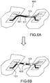
- figure 1 has a rectilinear configuration of the wires 101, 103, but a multitude of alternative shapes can be envisaged, the wires 101, 103 being able for example to overlap, as in the example illustrated by the figures 3 , 4B Where 6B .
- the son 101, 103 can, during a shaping step, be worn in an arrangement illustrated by a third configuration C, similar to the arrangement described above with reference to figure 1 , by means of an appropriate tool 200.
- the tool 200 can in particular comprise a head which can be brought during the shaping step into contact with the two wires 101, 103.
- a vertical translational movement can be applied to the head of the tool 200 so that the wires 101, 103 are shaped over a determined length, advantageously as long as possible as described above.
- the head of the tool 200 can be profiled so as to accommodate the outside diameters of the two wires 101, 103.
- the head of the tool 200 may include two grooves 201, 203 provided for this purpose.
- the vertical translation is conventionally defined with respect to a horizontal plane in which the interconnection areas 110a, 110b of the first element 110 can be located as well as the interconnection areas 120a, 120b of the second element 120.
- the bottom of each of the grooves 201 and 203 is arranged in a horizontal plane.
- characteristic impedances typically much greater than 50 Ohms.
- the figure 3 presents perspective views illustrating the shaping of an interconnection device by means of specific tooling, in another exemplary embodiment of the invention.
- the figure 3 presents three configurations A, B and C respectively reflecting an interconnection device at the end of a micro-wiring step, during a shaping step, and at the end of the shaping step.
- the arrangement of the wires 101, 103 at the end of the shaping step is, in the example of figure 3 , different from the provision presented in figure 2 or the figure 1 .
- the wires 101, 103 can overlap at least over part of their length, so as to promote coupling between the wires and also to reinforce the two-wire structure.
- a two-wire structure produced in this way has the particular advantage of being less sensitive to vibrations and mechanical shocks. It also makes it possible to ensure greater interconnection lengths.
- the twisted wires are wound up relative to each other before finalizing the cabling operations.
- the two wires of a pair of twisted wires must be cut to length, stripped and connected to the pads simultaneously. This is very difficult to achieve, in particular for wire lengths less than 1mm.
- the overlap is achieved using two separate unit wires cut to length, stripped and connected separately from one another. After connecting the two wires on their respective interconnection pads, the overlap consists in passing one of the wires above the other at least over part of its length.
- Such shaping can be obtained by applying a specific tool 300 comprising at least one head, the head of the tool 300 being configured so as to be able to guarantee the desired shaping to the two wires 101, 103, for example when the head of the tool 300 is driven by a rotational movement around its main axis by appropriate means, not shown in the figure, as well as a vertical translational movement along the portion of interest of the son 101, 103, that is to say along the portion along which it is desired that the son 101, 103 are overlapped.
- the profile of the head can be formed by two cylindrical pins 301, 303 or rollers, the outer diameters of which come into contact with the outer diameters of the wires 101, 103.
- each of the wires 101 and 103 may have a vertex, 101a and 103a respectively.
- Summit 101a is located closer to the element 120 than the element 110.
- the vertex 103a is disposed closer to the element 110 than to the element 120.
- the vertices 101a and 103a are arranged at different dimensions. measured along the wires from the first element 110 to the second element 120.
- the interconnection pads may or may not be arranged in the same horizontal plane.
- the shapes of the grooves 201 and 203 are adapted accordingly.
- the elements can remain stationary and the corresponding tool moves. Equivalently, the tool can be fixed and the movements are applied to the elements to be interconnected.
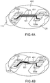
- FIGS. 4A and 4B present perspective views illustrating in a simplified manner interconnection devices according to alternative embodiments of the invention.
- an interconnection device 400 can be formed by a two-wire line comprising two wires 101, 103 in a configuration similar to the configuration described above with reference to figure 1 .
- at least part of the length of the bifilar line for example at least part of the portion of the wires 101, 103 along which they are substantially rectilinear and parallel to one another in this example embodiment, can be globally coated with a dielectric material 401.
- the coating by the dielectric 401 can extend even more widely, for example over the entire length of the wires 101, 103, or even also over the interconnection areas 110a, 110b and 120a, 120b respectively of the two elements to be interconnect 110, 120, that is to say in a region illustrated by the dotted lines in the figure 4A .
- the same characteristics can also be applied to an alternative configuration of the wires 101, 103 in which the wires 101, 103 overlap alternately, like the embodiment described above with reference to figure 3 .
- at least part of the length of the bifilar line for example at least part of the portion of the threads 101, 103 along which the latter are overlapped in this exemplary embodiment, can be generally coated with a material. dielectric 401.
- the coating by the dielectric 401 can extend even more widely, for example over the entire length of the wires 101, 103, or even also over the interconnection areas 110a, 110b and 120a, 120b respectively of the two elements to be interconnect 110, 120, that is to say in a region illustrated by the dotted lines in the figure 4A .
- An interconnection by an interconnection device 400 according to one of the embodiments illustrated by the figures 4A and 4B can be carried out by a method in which an additional coating step, following the aforementioned shaping step, allows the production of the dielectric coating 401.
- the embodiments illustrated by figures 4A and 4B can allow the achievement of characteristic impedances close to or greater than 50 Ohms.
- FIGS. 5A and 5B present perspective views illustrating in a simplified manner interconnection devices according to alternative embodiments of the invention.
- an interconnection device 500 can be formed by a two-wire line comprising two wires 101, 103 in a configuration similar to the configuration described above, for example with reference to figure 1 .
- at least part of the length of each wire 101, 103 for example at least part of the portion of each wire 101, 103 along which the wires 101, 103 are substantially rectilinear and parallel to one another.
- at least one wire can be insulated like the embodiments described above, or even the two wires 101, 103 may not be insulated and simply encased in dielectric material.
- an interconnection device 500 as described above can advantageously comprise one or a plurality of conductive elements 505 arranged in contact with the outer diameters of the wires 101, 103 covered with dielectric material 501, 503.
- the conductive elements 505 make it possible to adjust the impedance matching.
- An interconnection by means of interconnection devices according to the embodiments described above with reference to figures 5B and 6B can be carried out by means of a method comprising, in addition to the aforementioned micro-wiring, shaping and coating steps, an additional step of arranging the conductive elements .
- the conductive elements can for example be arranged by crimping, gluing, welding or by any other suitable technique.
- the two-wire connections are produced exclusively by means of the wires, their insulation and possibly a localized overall coating and / or a dielectric coating and / or conductive elements. These structures in particular do not require the presence of external shielding.
- connections for the interconnection of several elements for example three elements, by means of a plurality of wires having several zones capable of being fixed and electrically connected to the interconnection areas of the elements to be interconnected.
- a two-wire link can be formed by two conductive wires, the ends of each of which are connected to interconnection pads of two first elements to be interconnected, like the embodiments described above, and part of which center of each is stripped so as to be able to be fixed to the connection pads of a third element to be interconnected, disposed substantially between the first two elements to be interconnected.
- Another advantage of the present invention is that it allows interconnection of elements whose interconnection pads are arranged at different heights, for example with respect to the main plane of an electronic circuit board on which the elements to be interconnected. are fixed.
- the interconnection thus produced is also robust with respect to possible variations in temperature which may generate variations in the relative heights or distances of the various elements to be interconnected, or else to vibrations or other mechanical stresses.
Description
La présente invention concerne un procédé d'interconnexion pour circuits électroniques, notamment des circuits électroniques hyperfréquence, par fils parallèles couplés. La présente invention a également pour objet un outillage pour la réalisation d'une interconnexion au moyen du procédé. Elle s'applique notamment aux liaisons électroniques entre différents circuits électroniques.The present invention relates to an interconnection method for electronic circuits, in particular microwave electronic circuits, by coupled parallel wires. A subject of the present invention is also a tool for producing an interconnection by means of the method. It applies in particular to electronic links between different electronic circuits.
La présente invention concerne des applications pour lesquelles des liaisons électriques sont requises, entre différents circuits électroniques. Pour la suite, la notion de circuit électronique est à comprendre dans son acception la plus large, c'est-à-dire qu'un circuit électronique peut se présenter sous la forme d'un module électronique, par exemple d'une puce, d'un microsystème électromécanique, habituellement désigné sous l'acronyme de "MEMS", pour l'expression anglo-saxonne de "Micro-Electro-Mechanical System", d'un circuit intégré en boîtier, d'un module de cartes imprimées simples ou empilées, d'un module tridimensionnel, etc. Ces liaisons peuvent relier électriquement des circuits électroniques physiquement homogènes : par exemple des puces entre elles, ou bien des circuits électroniques physiquement hétérogènes, lorsqu'il s'agit par exemple de relier électriquement une puce à un support d'interconnexion avec un substrat, une carte imprimée, un boîtier, etc. Les signaux considérés peuvent être de caractère numérique rapide ou bien analogique hyperfréquence.The present invention relates to applications for which electrical connections are required, between different electronic circuits. For the following, the notion of electronic circuit is to be understood in its broadest sense, that is to say that an electronic circuit can be in the form of an electronic module, for example a chip, of a micromechanical system, usually designated by the acronym of "MEMS", for the English expression of "Micro-Electro-Mechanical System", of an integrated circuit in a package, of a module of simple printed boards or stacked, of a three-dimensional module, etc. These connections can electrically connect electronic circuits that are physically homogeneous: for example chips between them, or else physically heterogeneous electronic circuits, when it is a question for example of electrically connecting a chip to an interconnection support with a substrate, a printed card, case, etc. The signals considered can be fast digital in character or microwave analog.
Plus particulièrement, la présente invention se rapporte à des applications dans lesquelles les liaisons électriques précitées sont destinées à la transmission de signaux électriques occupant une large bande de fréquences, et/ou qui se situent dans des fréquences élevées en regard des dimensions des liaisons à réaliser, et/ou qui présentent des puissances élevées. Les signaux considérés peuvent être de nature analogique ou numérique. Il est par exemple considéré que des fréquences élevées en regard des dimensions des liaisons à réaliser, répondent à l'inégalité ll>3.109/1000.f, Il représentant la longueur de liaison en mètres, et f la fréquence du signal transmis, en Hertz.More particularly, the present invention relates to applications in which the aforementioned electrical connections are intended for the transmission of electrical signals occupying a wide band of frequencies, and / or which are located in high frequencies with regard to the dimensions of the connections to be made. , and / or which have high powers. The signals considered can be analog or digital in nature. It is for example considered that high frequencies with regard to the dimensions of the connections to be made, respond to the inequality ll> 3.10 9 /1000.f, It represents the link length in meters, and f the frequency of the transmitted signal, in Hertz.
Lorsque cette inégalité n'est pas satisfaite, la liaison réalisée est d'autant plus difficile à compenser que l'impédance caractéristique des interfaces est faible, que le niveau d'adaptation requis est élevé, et que la bande de fréquences d'intérêt est large. L'implantation d'un réseau d'adaptation n'est pas toujours possible, soit parce que la place disponible est insuffisante, soit parce que les éléments à interconnecter sont figés et non modifiables.When this inequality is not satisfied, the link produced is all the more difficult to compensate for the lower the characteristic impedance of the interfaces, the higher the level of adaptation required, and the higher the frequency band of interest. large. The installation of an adaptation network is not always possible, either because the available space is insufficient, or because the elements to be interconnected are fixed and not modifiable.
Dans le but de limiter l'influence parasite des éléments de liaison, réalisés par exemple sous la forme de fils ou de rubans, les circuits électroniques qui doivent être reliés électriquement sont placés à la plus grande proximité possible les uns des autres. Les fixations entre les éléments sont par exemple réalisées par des techniques de thermo-compression ou de thermo-sonie. En conséquence, les dimensions et les tolérances qui y sont associées et qui sont associées au positionnement des éléments, sont réduites, au détriment des coûts de réalisation et des rendements de fabrication. Lorsque les circuits électroniques sont reliés par des fils, il est toujours délicat de maîtriser l'écartement des fils de liaison, et un approchement substantiel de fils de liaison peut entraîner une mise en contact de ceux-ci, et partant un court-circuit. Dès lors, l'impédance caractéristique d'une ligne bifilaire réalisée au moyen de fils peut être typiquement très supérieure à 50 Ohms.In order to limit the parasitic influence of the connecting elements, produced for example in the form of wires or tapes, the electronic circuits which must be electrically connected are placed as close as possible to each other. The fixings between the elements are for example made by thermo-compression or thermo-sound techniques. Consequently, the dimensions and the tolerances which are associated therewith and which are associated with the positioning of the elements, are reduced, to the detriment of the production costs and the production yields. When the electronic circuits are connected by wires, it is always difficult to control the spacing of the connecting wires, and a substantial approach of the connecting wires can cause them to come into contact, and hence a short-circuit. Consequently, the characteristic impedance of a two-wire line produced by means of wires can typically be much greater than 50 Ohms.
Cet inconvénient est d'autant plus critique que les assemblages considérés sont complexes et que de longues chaînes de dimensions sont impliquées. Par exemple, dans un cas relativement simple où des puces ou des modules de puissance sont montés sur des dissipateurs thermiques, au travers de cavités réalisées dans un substrat, une chaîne de dimensions peut être définie comme la somme de la distance de la plage de connexion sur le substrat par rapport au bord du substrat, de la distance du bord du substrat au bord de la puce ou du module, et de la distance du bord de la puce ou du module, à la plage de connexion sur la puce ou le module. Une tolérance fine associée à une telle chaîne de dimensions est réalisable en pratique, mais au prix de procédés de fabrication et de contrôle nécessairement coûteux, et au risque d'un rendement faible.This drawback is all the more critical as the assemblies considered are complex and as long chains of dimensions are involved. For example, in a relatively simple case where chips or power modules are mounted on heat sinks, through cavities made in a substrate, a dimension string can be defined as the sum of the distance from the connection pad. on the substrate from the edge of the substrate, the distance from the edge of the substrate to the edge of the chip or module, and the distance from the edge of the chip or module, to the bond pad on the chip or module . A fine tolerance associated with such a chain of dimensions is achievable in practice, but at the cost of necessarily expensive manufacturing and control processes, and at the risk of low efficiency.
Un autre problème se posant dans ce contexte, est lié au fait qu'il est parfois nécessaire de relier des composants dans des assemblages dans lesquels ceux-ci présentent des points de fixation situés à des hauteurs différentes. Dans de tels cas, non seulement la différence de hauteur entre les composants ou circuits accroit la longueur de liaison, mais en outre la réalisation d'un retour de masse s'avère délicate.Another problem that arises in this context is linked to the fact that it is sometimes necessary to connect components in assemblies in which they have fixing points located at different heights. In such cases, not only does the difference in height between the components or circuits increase the link length, but also the realization of a ground return is difficult.
Il existe des solutions connues de l'état de la technique, mises en œuvre pour limiter l'influence des phénomènes parasites ou la désadaptation des connexions.There are solutions known from the state of the art, implemented to limit the influence of parasitic phenomena or the mismatching of the connections.
Une première technique connue consiste à utiliser des broches de connexion, dont les formes peuvent être diverses. Ces broches de connexion peuvent par exemple être des pointes traversantes, des lyres, ou encore des broches plates montées en surface de circuits imprimés. Un inconvénient de cette technique est qu'elle n'est pas efficace pour la transmission de signaux à haute fréquence, et pour la dissipation de fortes puissances.A first known technique consists in using connection pins, the shapes of which can be various. These connection pins can for example be through points, lyres, or even flat pins mounted on the surface of printed circuits. A drawback of this technique is that it is not efficient for the transmission of high frequency signals, and for the dissipation of high powers.
Une deuxième technique connue consiste à utiliser un micro-câblage comprenant une pluralité de fils conducteurs en parallèle, habituellement deux fils. Une telle technique est cependant souvent limitée par la surface disponible sur les plages de connexion, dont la surface est limitée par la fréquence des signaux à transmettre. Elle est également limitée par le phénomène d'inductance mutuelle entre les fils conducteurs.A second known technique consists in using micro-wiring comprising a plurality of conductor wires in parallel, usually two wires. Such a technique is however often limited by the area available on the connection pads, the area of which is limited by the frequency of the signals to be transmitted. It is also limited by the phenomenon of mutual inductance between the conducting wires.
Une troisième technique connue consiste à utiliser un micro-câblage comprenant des micro-rubans. Cette technique présente cependant également l'inconvénient d'être limitée par la surface disponible sur les plages de connexion, dont la surface est limitée par la fréquence des signaux à transmettre. Un autre inconvénient de cette technique est qu'elle est nettement plus coûteuse à mettre en œuvre de manière industrielle, en comparaison avec la deuxième technique filaire précitée.A third known technique consists in using micro-cabling comprising micro-ribbons. However, this technique also has the drawback of being limited by the area available on the connection pads, the area of which is limited by the frequency of the signals to be transmitted. Another drawback of this technique is that it is much more expensive to implement industrially, in comparison with the second aforementioned wire technique.
Une quatrième technique connue consiste à utiliser des microbilles conductrices, brasées entre des plages métallisées de modules montés retournés les uns par rapport aux autres. Cette technique est connue sous le nom de technique de "puce retournée", et plus habituellement désignée selon la terminologie anglo-saxonne "flip-chip". Par exemple, une puce électronique ou un module équipé d'une matrice de billes conductrices - souvent désignée selon le sigle BGA, de l'expression anglo-saxonne "Ball Grid Array" - monté retourné sur un substrat. Cette technique est avantageuse pour des liaisons à très haute fréquence, et/ou à très large bande de fréquences. Cependant, cette technique est coûteuse à mettre en œuvre de manière industrielle, et requiert des étapes supplémentaires dans le procédé de fabrication des dispositifs les mettant en œuvre. En outre, cette technique présente l'inconvénient de ne pas être efficace en termes de dissipation thermique, lorsqu'elle est appliquée à des circuits électroniques monolithiques, de type puce. Elle peut s'avérer efficace lorsqu'elle est appliquée à des modules intégrant un dissipateur thermique, mais dans de tels cas la technique s'avère globalement très coûteuse à mettre en œuvre de manière industrielle. Cette technique présente également l'inconvénient de nécessiter des puces ou des modules conçus spécifiquement pour ce type d'assemblages. Elle présente enfin un inconvénient lié à la difficulté, voire l'impossibilité, de réaliser des contrôles visuels sur les liaisons après assemblage.A fourth known technique consists in using conductive microbeads, brazed between metallized areas of modules mounted upside down with respect to one another. This technique is known under the name of “flip-chip” technique, and more usually designated according to the English terminology “flip-chip”. For example, an electronic chip or a module equipped with a matrix of conductive balls - often designated by the acronym BGA, from the Anglo-Saxon expression “Ball Grid Array” - mounted upside down on a substrate. This technique is advantageous for links at very high frequency, and / or at very wide frequency band. However, this technique is expensive to implement industrially, and requires additional steps in the manufacturing process of the devices implementing them. In addition, this technique has the drawback of not being efficient in terms of heat dissipation, when it is applied to monolithic electronic circuits, of chip type. It can prove to be effective when it is applied to modules incorporating a heat sink, but in such cases the technique turns out to be very expensive overall to implement industrially. This technique also has the drawback of requiring chips or modules designed specifically for this type of assembly. Finally, it has a drawback linked to the difficulty, or even the impossibility, of carrying out visual checks on the connections after assembly.
Une cinquième technique connue consiste à utiliser des micro-plages de connexion, assemblées directement par brasure ou par collage sur des circuits électroniques montés retournés l'une par rapport à l'autre. Cette technique est similaire à la quatrième technique connue utilisant des microbilles, décrite ci-dessus. Par exemple, une puce électronique ou un module équipé d'une matrice de micro-plages métallisées de connexion - souvent désignée selon le sigle LGA, de l'expression anglo-saxonne "Land Grid Array" - monté retourné sur un substrat. Cette technique permet également de réaliser des liaisons à très haute fréquence et/ou très large bande. En revanche, cette technique n'est pas efficace pour assurer l'adaptation des différences de coefficients de dilatation entre les différents circuits électroniques. D'une manière similaire à la quatrième technique décrite ci-dessus, cette technique présente l'inconvénient de ne pas être efficace en termes de dissipation thermique, lorsqu'elle est appliquée à des circuits électroniques monolithiques, de type puce. Elle peut également s'avérer efficace lorsqu'elle est appliquée à des modules intégrant un dissipateur thermique, mais au prix d'une mise en œuvre très coûteuse. Cette technique présente également l'inconvénient de nécessiter des puces ou des modules conçus spécifiquement pour ce type d'assemblages. Elle présente également un inconvénient lié à la difficulté, voire l'impossibilité, de réaliser des contrôles visuels des liaisons après assemblage, même lorsque certaines liaisons sont réalisées avec des plages qui remontent sur les côtés, par exemple pour des modules munis de castellations, selon des techniques spécifiques au LGA.A fifth known technique consists in using micro-connection pads, assembled directly by soldering or by gluing on electronic circuits mounted upside down with respect to one another. This technique is similar to the fourth known technique using microbeads, described above. For example, an electronic chip or a module equipped with a matrix of metallized connection micro-pads - often designated by the acronym LGA, from the English expression “Land Grid Array” - mounted upside down on a substrate. This technique also allows very high frequency and / or very wide band connections to be made. On the other hand, this technique is not effective in ensuring the adaptation of the differences in expansion coefficients between the different electronic circuits. In a manner similar to the fourth technique described above, this technique has the drawback of not being effective in terms of heat dissipation, when it is applied to monolithic electronic circuits, of chip type. It can also prove to be effective when it is applied to modules integrating a heat sink, but at the cost of a very expensive implementation. This technique also has the drawback of requiring chips or modules designed specifically for this type of assembly. She also has a drawback linked to the difficulty, or even the impossibility, of carrying out visual checks of the connections after assembly, even when some connections are made with areas which go up on the sides, for example for modules provided with castellations, according to techniques specific to the LGA.
Une sixième technique connue consiste à utiliser des micro-plots de connexion destinés à la réalisation de liaisons par thermo-compression ou par collage. Cette technique permet la réalisation de liaisons à très haute fréquence et/ou à très large bande de fréquences. Cependant, cette technique ne permet pas d'assurer une dissipation thermique efficace. Elle présente également un inconvénient lié à la difficulté, voire l'impossibilité, de réaliser des contrôles visuels des liaisons après assemblage.A sixth known technique consists in using micro-connection pads intended for making connections by thermo-compression or by gluing. This technique enables very high frequency and / or very wide frequency band connections to be made. However, this technique does not make it possible to ensure efficient heat dissipation. It also has a drawback linked to the difficulty, or even the impossibility, of carrying out visual checks of the connections after assembly.
Une septième technique connue consiste en un collage automatique par bande, cette technique est habituellement désignée selon l'acronyme "TAB", pour l'expression anglo-saxonne de "Tape Automated Bonding". Cette technique se base sur un circuit électrique réalisé sur un substrat fin et souple, dont les pistes dépassent et sont directement micro-câblées sur les plots d'interconnexion des éléments à relier, par exemple par thermo-compression ou par brasure collective. Cette technique permet un mode de liaison collectif, c'est-à-dire que toutes les opérations de connexion pour un même circuit imprimé, peuvent être réalisées de manière simultanée. La technique TAB permet par exemple la réalisation de liaisons avec des lignes de transmission coplanaires, de type masse / signal / masse. De telles lignes présentent l'inconvénient d'être sensibles aux dissymétries, de nécessiter un minimum de six points de contact par liaison, de nécessiter des plans de masse de large surface, ainsi qu'une grande finesse dans la réalisation de la ligne centrale, en termes de largeur de piste et d'écart avec les lignes de masse, dans le but d'obtenir des impédances caractéristiques typiques de l'ordre de 50 Ω.A seventh known technique consists of automatic tape bonding, this technique is usually designated by the acronym "TAB", for the English expression of "Tape Automated Bonding". This technique is based on an electrical circuit produced on a thin and flexible substrate, the tracks of which protrude and are directly micro-wired to the interconnection pads of the elements to be connected, for example by thermo-compression or by collective soldering. This technique allows a collective connection mode, that is to say that all the connection operations for the same printed circuit, can be carried out simultaneously. The TAB technique makes it possible, for example, to make connections with coplanar transmission lines, of the mass / signal / mass type. Such lines have the drawback of being sensitive to dissymmetries, of requiring a minimum of six contact points per connection, of requiring ground planes with a large surface area, as well as great finesse in the production of the central line, in terms of track width and distance from the ground lines, with the aim of obtaining typical characteristic impedances of the order of 50 Ω.
Les demandes de brevets japonaises
Un but de la présente invention est de pallier les inconvénients propres aux dispositifs connus précités, en proposant un procédé d'interconnexion pour circuits électroniques hyperfréquence, formé par au moins deux fils conducteurs, les fils étant, rapprochés et/ou mis en forme de sorte que la liaison ainsi pouvant se substituer aux techniques connues d'interconnexion, le plus souvent filaires, ou également aux lignes de transmission coplanaires de type masse / signal / masse utilisées pour la réalisation de liaisons selon des techniques de type TAB. Un procédé d'interconnexion selon l'invention permet la transmission de signaux électriques occupant une large bande de fréquences et/ou se situant à des fréquences élevées en regard des dimensions à réaliser et/ou présentant des puissances élevées, avec un niveau d'adaptation élevé.An aim of the present invention is to alleviate the drawbacks specific to the aforementioned known devices, by proposing an interconnection method for microwave electronic circuits, formed by at least two conducting wires, the wires being, brought together and / or shaped like so that the bond thus being able to replace the known techniques interconnection, most often wired, or also to coplanar transmission lines of mass / signal / mass type used for making connections according to TAB type techniques. An interconnection method according to the invention allows the transmission of electrical signals occupying a wide frequency band and / or located at high frequencies with regard to the dimensions to be achieved and / or having high powers, with a level of adaptation. raised.
La présente invention propose de relier électriquement les circuits électroniques au moyen d'un élément formant une ligne de transmission de longueur et d'impédance caractéristique appropriées, formé par des fils parallèles couplés.The present invention proposes to electrically connect the electronic circuits by means of an element forming a transmission line of appropriate length and characteristic impedance, formed by coupled parallel wires.
Un avantage de l'invention est de permettre la réalisation de liaisons électriques de type ligne à transmission, dont les dimensions permettent de relâcher les éléments d'une chaîne de dimensions, et d'éloigner les éléments interconnectés.An advantage of the invention is that it allows electrical connections of the transmission line type, the dimensions of which make it possible to relax the elements of a chain of dimensions, and to move the interconnected elements away.
Encore un autre avantage de l'invention est qu'elle permet de tolérer des variations de dimensions liées aux possibles variations de températures et aux différents coefficients de dilatation des matériaux mis en œuvre, pouvant typiquement induire des mouvements relatifs de l'ordre du micron.Yet another advantage of the invention is that it makes it possible to tolerate variations in dimensions linked to possible variations in temperature and to the various coefficients of expansion of the materials used, which can typically induce relative movements of the order of a micron.
Encore un autre avantage de l'invention est qu'un dispositif selon l'un des modes de réalisation décrits peut être réalisé au moyen d'un outillage usuel de micro-câblage. Un outillage de mise en forme des fils est proposé pour chacune des réalisations possibles. Ces outillages relativement simples peuvent être mis en œuvre sur la plupart des équipements de micro-câblage ou de placement automatisé de composants électroniques. Les formes des dispositifs proposés sont étroitement liées aux outils de mise en forme proposés.Yet another advantage of the invention is that a device according to one of the embodiments described can be produced by means of standard micro-wiring tools. A tool for shaping the wires is available for each of the possible embodiments. These relatively simple tools can be implemented on most micro-wiring or automated electronic component placement equipment. The shapes of the proposed devices are closely linked to the proposed formatting tools.
A cet effet, l'invention a pour objet un procédé d'interconnexion selon la revendication 1.To this end, the subject of the invention is an interconnection method according to claim 1.
Dans un mode de réalisation du procédé, à l'issue de l'étape de mise en forme, les fils se chevauchent sur au moins une partie de leur longueur le long de laquelle au moins un fil est recouvert de l'isolant.In one embodiment of the method, at the end of the shaping step, the wires overlap over at least part of their length along which at least one wire is covered with the insulation.
Dans un autre mode de réalisation du procédé, à l'issue de l'étape de mise en forme, les fils présentent une configuration rectiligne, les fils étant au moins sur cette portion disposés sensiblement en parallèle l'un de l'autre.In another embodiment of the method, at the end of the shaping step, the wires have a rectilinear configuration, the wires being at least on this portion arranged substantially in parallel with one another.
Avantageusement, à l'issue de l'étape de mise en forme, les fils sont rapprochés sur la plus grande longueur disponible de ceux-ci.Advantageously, at the end of the shaping step, the threads are brought together over the greatest available length thereof.
L'étape de mise en forme peut être suivie d'une étape d'enrobage lors de laquelle au moins un fil est enrobé d'un matériau diélectrique sur au moins une partie de sa longueur.The shaping step can be followed by a coating step during which at least one wire is coated with a dielectric material over at least part of its length.
Le matériau diélectrique peut enrober globalement lesdits au moins deux fils sur au moins une partie de leur longueur. Alternativement, chaque fil peut être indépendamment enrobé au moins sur une partie de sa longueur du matériau diélectrique.The dielectric material can globally coat said at least two wires over at least part of their length. Alternatively, each wire can be independently coated at least over part of its length with the dielectric material.
L'étape d'enrobage peut être à son tour suivie d'une étape additionnelle de disposition d'éléments conducteurs disposés au contact des diamètres extérieurs desdits au moins deux fils ; entre les fils, le nombre et la nature des éléments conducteurs étant configurés de manière à procurer une adaptation d'impédance souhaitée au dispositif d'interconnexion.The coating step may in turn be followed by an additional step of arranging conductive elements placed in contact with the outer diameters of said at least two wires; between the wires, the number and nature of the conductive elements being configured so as to provide a desired impedance match to the interconnection device.
L'invention a également pour objet un outil selon la revendication 9.The subject of the invention is also a tool according to claim 9.
Dans une machine portant l'outil et les éléments à interconnecter, les éléments peuvent rester fixes et l'outil se déplace. De façon équivalente, l'outil peut être fixe et les mouvements sont appliqués aux éléments à interconnecter.In a machine carrying the tool and the elements to be interconnected, the elements can remain stationary and the tool moves. Equivalently, the tool can be fixed and the movements are applied to the elements to be interconnected.
Les mouvements relatifs de translation peuvent être horizontaux et verticaux.The relative translational movements can be horizontal and vertical.
Avantageusement, la tête de l'outil est apte à se déplacer relativement par rapport auxdits au moins deux fils en translation le long d'au moins une partie de la longueur desdits au moins deux fils et comprend deux gorges aptes à recevoir chacun desdits au moins deux fils.Advantageously, the head of the tool is able to move relatively with respect to said at least two wires in translation along at least part of the length of said at least two wires and comprises two grooves adapted to receive each of said at least two sons.
Dans le mode de réalisation du dispositif où les fils se chevauchent la tête de l'outil est apte à se déplacer relativement par rapport auxdits au moins deux fils en translation et en rotation le long d'au moins une partie de la longueur desdits au moins deux fils et comprend deux pions cylindriques.In the embodiment of the device where the wires overlap, the head of the tool is able to move relatively with respect to said at least two wires in translation and in rotation along at least part of the length of said at least two wires and includes two cylindrical pawns.
D'autres caractéristiques et avantages de l'invention apparaîtront à la lecture de la description, donnée à titre d'exemple, faite en regard des dessins annexés qui représentent :
- la
figure 1 , une vue en perspective illustrant de manière simplifiée un dispositif d'interconnexion suivant un exemple de réalisation de l'invention ; - la
figure 2 , des vues en perspective illustrant la mise en forme d'un dispositif d'interconnexion au moyen d'un outillage spécifique, dans un exemple de réalisation de l'invention ; - la
figure 3 , des vues en perspective illustrant la mise en forme d'un dispositif d'interconnexion au moyen d'un outillage spécifique, dans un autre exemple de réalisation de l'invention ; - les
figures 4A et 4B , des vues en perspective illustrant de manière simplifiée des dispositifs d'interconnexions suivant des exemples de réalisation alternatifs de l'invention ; - les
figures 5A et 5B , des vues en perspective illustrant de manière simplifiée des dispositifs d'interconnexions suivant des exemples de réalisation alternatifs de l'invention ; - les
figures 6A, 6B , des vues en perspective illustrant de manière simplifiée des dispositifs d'interconnexions suivant des exemples de réalisation alternatifs de l'invention.
- the
figure 1 , a perspective view illustrating in a simplified manner an interconnection device according to an exemplary embodiment of the invention; - the
figure 2 , perspective views illustrating the shaping of an interconnection device by means of specific tooling, in an exemplary embodiment of the invention; - the
figure 3 , perspective views illustrating the shaping of an interconnection device by means of specific tooling, in another exemplary embodiment of the invention; - the
figures 4A and 4B , perspective views illustrating in a simplified manner interconnection devices according to alternative embodiments of the invention; - the
figures 5A and 5B , perspective views illustrating in a simplified manner interconnection devices according to alternative embodiments of the invention; - the
figures 6A, 6B , perspective views illustrating in a simplified manner interconnection devices according to alternative embodiments of the invention.
La
Le dispositif d'interconnexion 100 permet dans l'exemple illustré par la figure, l'interconnexion entre deux éléments 110, 120, par exemple des circuits ou modules électroniques. Chaque élément à interconnecter 110, 120 peut comprendre des plages d'interconnexion. Dans l'exemple illustré par la
Le dispositif d'interconnexion peut comprendre une ligne bifilaire formée par un premier fil 101, par exemple fil de masse, couplé à un second film 103, par exemple fil de signal. Le premier fil 101 peut être connecté au premier élément 110 via la première plage d'interconnexion 110a de celui-ci, et au second élément 120 via la première plage d'interconnexion 120a de ce dernier. D'une manière similaire, le second fil 103 peut être connecté au premier élément 110 via la seconde plage d'interconnexion 110b de celui-ci, et au second élément 120 via la seconde plage d'interconnexion 120b de ce dernier.The interconnection device may comprise a two-wire line formed by a
Les deux fils 101, 103 sont dans l'exemple illustré par la figure sensiblement parallèle, au moins sur une portion de ceux-ci. Selon une spécificité de la présente invention, au moins un des deux fils 101, 103 est recouvert d'une couche d'un matériau électriquement isolant. Des fils recouverts d'isolant sont en eux-mêmes connus, et peuvent être pourvus selon des circuits d'approvisionnement connus. D'une manière typique, la longueur de la liaison électrique assurée par le dispositif d'interconnexion 100 peut être de l'ordre de 100 µm, à quelques millimètres. L'épaisseur de la couche d'isolant sur au moins un des fils peut être de l'ordre du micromètre.The two
Le matériau isolant permet aux fils 101, 103 d'être possiblement physiquement en contact, sans qu'une liaison électrique ne puisse pour autant être établie entre les deux fils 101, 103. Avantageusement, les deux fils 101, 103 peuvent être recouverts d'isolant.The insulating material allows the
Les fils 101, 103 peuvent être disposés et mis en forme suivant des techniques de micro-câblage en elles-mêmes connues, c'est-à-dire qu'un procédé de mise en œuvre d'un dispositif d'interconnexion, dit pour la suite procédé d'interconnexion suivant la présente invention peut être dérivé d'un procédé connu de micro-câblage. Les fils 101, 103 peuvent par exemple être disposés dans une première étape de micro-câblage, puis mis en forme dans une étape de mise en forme, de manière à être approchés l'un de l'autre et de façon à obtenir une adaptation d'impédance souhaitée pour l'application envisagée. Les fils 101, 103 peuvent être rapprochés sur la plus grande longueur disponible de ceux-ci, c'est-à-dire que le rapprochement mutuel des fils 101, 103 est réalisé au plus près des plages d'interconnexion 110a, 110b et 120a, 120b.The
L'exemple illustré par la
D'une manière typique, la gamme d'impédances pouvant être réalisée au moyen d'un dispositif d'interconnexion suivant la présente invention peut notamment couvrir les valeurs typiques nominales de 30, 50 et 75 Ohms. La bande de fréquence visée peut être de l'ordre de quelques dizaines de GHz ou plus.
- La
figure 2 présente des vues en perspective illustrant la mise en forme d'un dispositif d'interconnexion au moyen d'un outillage spécifique, dans un exemple de réalisation de l'invention. - La
figure 2 présente une première configuration A dans laquelle deux éléments à interconnecter 110, 120 ont été reliés lors d'une étape de micro-câblage par une liaison bifilaire comprenant unpremier fil 101 et unsecond fil 103, les extrémités des fils 101, 103 ayant été fixées à des plages d'interconnexion, par exemple ou moyen de soudure, de brasure, de collage ou de tout autre moyen approprié.
- The
figure 2 presents perspective views illustrating the shaping of an interconnection device by means of specific tooling, in an exemplary embodiment of the invention. - The
figure 2 presents a first configuration A in which two elements to be interconnected 110, 120 have been connected during a micro-wiring step by a two-wire connection comprising afirst wire 101 and asecond wire 103, the ends of thewires
Dans une deuxième configuration B illustrée par la
La translation verticale est de façon conventionnelle définie par rapport à un plan horizontal dans lequel peuvent se situer les plages d'interconnexion 110a, 110b du premier élément 110 ainsi que les plages d'interconnexion 120a, 120b du second élément 120. Dans ce cas, le fond de chacune des gorges 201 et 203 est disposé dans un plan horizontal.The vertical translation is conventionally defined with respect to a horizontal plane in which the
Il est également possible de réaliser l'interconnexion d'éléments dont les plages sont situées à des hauteurs différentes, c'est-à-dire dans des plans horizontaux différents, voire dans des plans inclinés par rapport à un plan horizontal. Les formes des gorges 201 et 203 sont adaptées en conséquence et sont alors disposées dans des plans inclinés par rapport à un plan horizontal.It is also possible to interconnect elements whose areas are located at different heights, that is to say in different horizontal planes, or even in planes inclined with respect to a horizontal plane. The shapes of the
Il est possible de réaliser au moyen d'une telle structure des impédances caractéristiques typiquement très supérieures à 50 Ohms.It is possible to achieve by means of such a structure characteristic impedances typically much greater than 50 Ohms.
La
D'une manière similaire à la
Il ne s'agit pas d'une paire de fils torsadés qui serait beaucoup plus compliquée à mettre en œuvre. En effet, les fils torsadés sont enroulés l'un par rapport à l'autre avant de finaliser les opérations de câblage. Les deux fils d'une paire de fils torsadés doivent être mis à longueur, dénudés et raccordés sur les plages simultanément. Ceci est très délicat à réaliser notamment pour des longueurs de fils inférieures à 1mm. Le chevauchement est en revanche réalisé à l'aide de deux fils unitaires séparés mis à longueur, dénudés et raccordés séparément l'un de l'autre. Après raccordement des deux fils sur leurs plages d'interconnexion respectives, le chevauchement consiste à faire passer un des fils au dessus de l'autre au moins sur une partie de sa longueur.It is not a twisted pair of wires which would be much more complicated to implement. In fact, the twisted wires are wound up relative to each other before finalizing the cabling operations. The two wires of a pair of twisted wires must be cut to length, stripped and connected to the pads simultaneously. This is very difficult to achieve, in particular for wire lengths less than 1mm. On the other hand, the overlap is achieved using two separate unit wires cut to length, stripped and connected separately from one another. After connecting the two wires on their respective interconnection pads, the overlap consists in passing one of the wires above the other at least over part of its length.
Une telle mise en forme peut être obtenue par l'application d'un outil spécifique 300 comprenant au moins une tête, la tête de l'outil 300 étant configurée de manière à pouvoir garantir la mise en forme souhaitée aux deux fils 101, 103, par exemple lorsque la tête de l'outil 300 est animée d'un mouvement de rotation autour de son axe principal par des moyens appropriés, non représentés sur la figure, ainsi que d'un mouvement de translation verticale le long de la portion d'intérêt des fils 101, 103, c'est-à-dire le long de la portion le long de laquelle il est souhaité que les fils 101, 103 soient chevauchés. Ainsi que dans l'exemple illustré par la
Pour faciliter le chevauchement alternatif des deux fils 101 et 103, il est possible de former les fils 101 et 103 de façon non parallèle lors de leur raccordement sur leurs plages respectives avant application de l'outil 300. Plus précisément, chacun des fils 101 et 103 peut posséder un sommet, respectivement 101a et 103a. Le sommet 101a est disposé plus près de l'élément 120 que de l'élément 110. Inversement, le sommet 103a est disposé plus près de l'élément 110 que de l'élément 120. De façon plus générale, les sommets 101a et 103a sont disposés à des cotes différentes, cotes mesurées le long des fils du premier élément 110 vers le second élément 120. Ainsi, lors de l'application de l'outil 300, le sommet 101a recouvre facilement le fil 103 et le sommet 103a recouvre facilement le fil 101.To facilitate the alternating overlap of the two
Comme précédemment, les plages interconnexion peuvent ou non être disposées dans un même plan horizontal. Les formes des gorges 201 et 203 sont adaptées en conséquence.As previously, the interconnection pads may or may not be arranged in the same horizontal plane. The shapes of the
Dans une machine portant les outils représentés sur les
Les
En référence à la
Avantageusement encore, l'enrobage par le diélectrique 401 peut s'étendre plus largement encore, par exemple sur toute la longueur des fils 101, 103, voire également sur les plages d'interconnexion 110a, 110b et 120a, 120b respectivement des deux éléments à interconnecter 110, 120, c'est-à-dire dans une région illustrée par les traits pointillés dans la
Maintenant en référence à la
Avantageusement encore, l'enrobage par le diélectrique 401 peut s'étendre plus largement encore, par exemple sur toute la longueur des fils 101, 103, voire également sur les plages d'interconnexion 110a, 110b et 120a, 120b respectivement des deux éléments à interconnecter 110, 120, c'est-à-dire dans une région illustrée par les traits pointillés dans la
Une interconnexion par un dispositif d'interconnexion 400 suivant l'un des modes de réalisation illustrés par les
D'une manière typique, les modes de réalisation illustrés par les
Les
En référence à la
Maintenant en référence à la
Un dispositif d'interconnexion 500 selon le mode de réalisation décrit en référence à la
- Les
figures 6A et 6B présentent des vues en perspective illustrant de manière simplifiée des dispositifs d'interconnexions suivant des exemples de réalisation alternatifs de l'invention. - La
figure 6A présente un mode de réalisation similaire au mode de réalisation illustré par lafigure 4B décrite précédemment, dans lequel les fils 101, 103 formant la ligne bifilaire d'un dispositif d'interconnexion 600 sont chevauchés, et recouverts d'un matériau diélectrique 601. - La
figure 6B illustre un dispositif d'interconnexion similaire au dispositif d'interconnexion 600 illustré par lafigure 6A , comprenant en outre un ou une pluralité d'éléments conducteurs 605 disposés au contact de la surface extérieure de l'enrobage de matériau diélectrique 601 réalisé autour des fils 101, 103.
- The
figures 6A and 6B present perspective views illustrating in a simplified manner interconnection devices according to alternative embodiments of the invention. - The
figure 6A presents an embodiment similar to the embodiment illustrated byfigure 4B described above, in which thewires interconnection device 600 are overlapped, and covered with adielectric material 601. - The
figure 6B illustrates an interconnection device similar to theinterconnection device 600 illustrated byfigure 6A , further comprising one or a plurality ofconductive elements 605 disposed in contact with the outer surface of the coating ofdielectric material 601 formed around thewires
Une interconnexion au moyen de dispositifs d'interconnexion suivant les modes de réalisation décrits ci-dessus en référence aux
Il est à noter que dans les différents modes de réalisation présentés ci-dessus, les liaisons bifilaires sont réalisées exclusivement au moyen des fils, de leur isolant et possiblement d'un enrobage global localisé et/ou d'un enrobage de diélectrique et/ou d'éléments conducteurs. Ces structures ne requièrent notamment pas la présence d'un blindage externe.It should be noted that in the various embodiments presented above, the two-wire connections are produced exclusively by means of the wires, their insulation and possibly a localized overall coating and / or a dielectric coating and / or conductive elements. These structures in particular do not require the presence of external shielding.
Il est à observer que les modes de réalisation décrits précédemment sont des exemples non-limitatifs de la présente invention. Des combinaisons des caractéristiques présentées dans les différents modes de réalisation peuvent notamment être combinées. Selon le même concept inventif, il est également notamment possible de réaliser des liaisons tri-filaires ou multifilaires, par exemple des liaisons de type Masse / Signal / Masse.It should be observed that the embodiments described above are non-limiting examples of the present invention. Combinations of the characteristics presented in the various embodiments can in particular be combined. According to the same inventive concept, it is also in particular possible to produce three-wire or multi-wire connections, for example connections of the Ground / Signal / Ground type.
Egalement, il est possible de réaliser des liaisons pour l'interconnexion de plusieurs éléments, par exemple trois éléments, au moyen d'une pluralité de fils présentant plusieurs zones aptes à être fixées et reliées électriquement à des plages d'interconnexion des éléments à interconnecter. Par exemple, une liaison bifilaire peut être formée par deux fils conducteurs dont les extrémités de chacun sont reliées à des plages d'interconnexion de deux premiers éléments à interconnecter, à l'instar des modes de réalisation décrits ci-dessus, et dont une partie centrale de chacun est dénudée de manière à pouvoir être fixée à des plages de connexion d'un troisième élément à interconnecter, disposé sensiblement entre les deux premiers éléments à interconnecter.Also, it is possible to make connections for the interconnection of several elements, for example three elements, by means of a plurality of wires having several zones capable of being fixed and electrically connected to the interconnection areas of the elements to be interconnected. . For example, a two-wire link can be formed by two conductive wires, the ends of each of which are connected to interconnection pads of two first elements to be interconnected, like the embodiments described above, and part of which center of each is stripped so as to be able to be fixed to the connection pads of a third element to be interconnected, disposed substantially between the first two elements to be interconnected.
Un autre avantage de la présente invention est qu'elle permet une interconnexion d'éléments dont les plages d'interconnexion sont disposées à des hauteurs différentes, par exemple par rapport au plan principal d'une carte de circuit électronique sur laquelle les éléments à interconnecter sont fixés. L'interconnexion ainsi réalisée est en outre robuste vis-à-vis de possibles variations de température pouvant engendrer des variations des hauteurs ou distances relatives des différents éléments à interconnecter, ou bien à des vibrations ou autres sollicitations mécaniques.Another advantage of the present invention is that it allows interconnection of elements whose interconnection pads are arranged at different heights, for example with respect to the main plane of an electronic circuit board on which the elements to be interconnected. are fixed. The interconnection thus produced is also robust with respect to possible variations in temperature which may generate variations in the relative heights or distances of the various elements to be interconnected, or else to vibrations or other mechanical stresses.
Claims (11)
- An interconnection method for conveying microwave signals between elements (110, 120) to be interconnected, such as electronic modules or circuits, comprising at least two coupled lines formed by at least two wires (101, 103) capable of being electrically connected to interconnection areas (110a, 110b, 120a, 120b) of the elements (110, 120) to be interconnected, with at least one of the wires being covered by an insulator on at least one portion thereof, characterised in that it comprises at least one step of micro-wiring, during which step the wires (101, 103) are connected to the interconnection areas (110a, 110b, 120a, 120b) of the elements (110, 120) to be interconnected, followed by a step of bringing together and/or of shaping said at least two wires (101, 103), during which step said at least two wires (101, 103) are disposed in their desired configuration so as to provide desired impedance matching between the elements (110, 120) to be interconnected.
- The interconnection method as claimed in claim 1, characterised in that, on completion of the shaping step, the wires (101, 103) overlap on at least part of the length thereof, along which at least one wire is covered with insulator.
- The interconnection method as claimed in claim 1, characterised in that, on completion of the shaping step, the wires (101, 103) have a straight configuration, the wires (101, 103) being disposed, at least on this portion, substantially parallel to each other.
- The method as claimed in any one of the preceding claims, characterised in that, on completion of the shaping step, the wires (101, 103) are brought together on the longest available length thereof.
- The method as claimed in any of the preceding claims, characterised in that the shaping step is followed by a coating step, during which step at least one wire (101, 103) is coated with a dielectric material (401, 501, 503, 601) on at least part of the length thereof.
- The interconnection method as claimed in claim 5, characterised in that the dielectric material (401) generally coats said at least two wires (101, 103) on at least part of the length thereof.
- The interconnection method as claimed in claim 5, characterised in that each wire (101, 103) is independently coated with the dielectric material (401) on at least part of the length thereof.
- The interconnection method as claimed in any of claims 5 to 7, characterised in that the coating step is followed by an additional step of arranging conductive elements (505, 605) arranged in contact with the external diameters of said at least two wires (101, 103), between the wires (101, 103), with the number and the nature of the conductive elements (505, 605) being configured so as to provide the interconnection device (100, 500) with desired impedance matching.
- A tool (200, 300) for implementing an interconnection method according to any one of the preceding claims, comprising a head capable of moving relatively in relation to said at least two wires (101, 103) by translation and/or by rotation along at least part of the length of said at least two wires (101, 103), the profile of the head being configured to bring together and/or shape the wires (101, 103) so that they can be supported in a desired configuration during the movement of the head, so as to provide desired impedance matching between the elements (110, 120) to be interconnected.
- The tool (200) as claimed in claim 9, characterised in that the head is capable of moving relatively in relation to said at least two wires (101, 103) by translation, and comprises two grooves (201, 203) capable of accommodating each of said at least two wires (101, 103).
- The tool (300) as claimed in claim 9, characterised in that the head is capable of moving relatively in relation to said at least two wires (101, 103) by translation and by rotation, and comprises two cylindrical pins (301, 303).
Applications Claiming Priority (1)
| Application Number | Priority Date | Filing Date | Title |
|---|---|---|---|
| FR1300465A FR3002814B1 (en) | 2013-03-01 | 2013-03-01 | INTERCONNECTION DEVICE FOR ELECTRONIC CIRCUITS BY COUPLED PARALLEL THREADS, AND METHOD AND TOOLING RELATING THERETO |
Publications (3)
| Publication Number | Publication Date |
|---|---|
| EP2772936A2 EP2772936A2 (en) | 2014-09-03 |
| EP2772936A3 EP2772936A3 (en) | 2017-02-08 |
| EP2772936B1 true EP2772936B1 (en) | 2021-12-29 |
Family
ID=48979790
Family Applications (1)
| Application Number | Title | Priority Date | Filing Date |
|---|---|---|---|
| EP14157235.4A Active EP2772936B1 (en) | 2013-03-01 | 2014-02-28 | Method of wire bonding parallel bond wires aswell as a reshaping process of the same, and the related apparatus |
Country Status (3)
| Country | Link |
|---|---|
| EP (1) | EP2772936B1 (en) |
| ES (1) | ES2907023T3 (en) |
| FR (1) | FR3002814B1 (en) |
Families Citing this family (1)
| Publication number | Priority date | Publication date | Assignee | Title |
|---|---|---|---|---|
| CN112701092A (en) * | 2020-12-24 | 2021-04-23 | 北京国联万众半导体科技有限公司 | Millimeter wave monolithic integrated circuit packaging structure and packaging method thereof |
Family Cites Families (10)
| Publication number | Priority date | Publication date | Assignee | Title |
|---|---|---|---|---|
| JP2897086B2 (en) * | 1991-06-21 | 1999-05-31 | 株式会社村田製作所 | Positioning and fixing of lead wires to electronic components |
| JP2763445B2 (en) * | 1992-04-03 | 1998-06-11 | 三菱電機株式会社 | High frequency signal wiring and bonding device therefor |
| US5459284A (en) * | 1993-08-31 | 1995-10-17 | Motorola, Inc. | Twisted-pair wire bond and method thereof |
| JP2000323907A (en) * | 1999-05-07 | 2000-11-24 | Nec Corp | Microwave ic connection line |
| JP3915723B2 (en) * | 2003-03-25 | 2007-05-16 | 株式会社デンソー | Wire bonding method |
| JP2005064248A (en) * | 2003-08-12 | 2005-03-10 | Renesas Technology Corp | Semiconductor device and manufacturing method thereof |
| US6992377B2 (en) * | 2004-02-26 | 2006-01-31 | Freescale Semiconductor, Inc. | Semiconductor package with crossing conductor assembly and method of manufacture |
| US20060175712A1 (en) * | 2005-02-10 | 2006-08-10 | Microbonds, Inc. | High performance IC package and method |
| US7741720B2 (en) * | 2007-09-25 | 2010-06-22 | Silverbrook Research Pty Ltd | Electronic device with wire bonds adhered between integrated circuits dies and printed circuit boards |
| JP2009158839A (en) * | 2007-12-27 | 2009-07-16 | Sharp Corp | Semiconductor package, semiconductor device and wire bonding method |
-
2013
- 2013-03-01 FR FR1300465A patent/FR3002814B1/en not_active Expired - Fee Related
-
2014
- 2014-02-28 ES ES14157235T patent/ES2907023T3/en active Active
- 2014-02-28 EP EP14157235.4A patent/EP2772936B1/en active Active
Also Published As
| Publication number | Publication date |
|---|---|
| FR3002814B1 (en) | 2016-06-24 |
| EP2772936A3 (en) | 2017-02-08 |
| ES2907023T3 (en) | 2022-04-21 |
| EP2772936A2 (en) | 2014-09-03 |
| FR3002814A1 (en) | 2014-09-05 |
Similar Documents
| Publication | Publication Date | Title |
|---|---|---|
| FR2945895A1 (en) | INTERCONNECTION DEVICE FOR ELECTRONIC CIRCUITS, ESPECIALLY HYPERFREQUENCY ELECTRONIC CIRCUITS | |
| EP0734063A2 (en) | Integrated circuit micromodule obtained by continuous assembly of patterned strips | |
| FR2596607A1 (en) | METHOD FOR MOUNTING AN INTEGRATED CIRCUIT ON A CIRCUIT BOARD, INTEGRATED CIRCUIT BOX AND INTEGRATED CIRCUIT BOARD FOR IMPLEMENTING THE METHOD | |
| EP2158604A2 (en) | Assemblage of radiofrequency chips | |
| EP0424262B1 (en) | Portable electronics with connectable components | |
| EP3579286B1 (en) | Photonic chip penetrated by a via | |
| FR3007403A1 (en) | METHOD FOR PRODUCING A MECHANICALLY AUTONOMOUS MICROELECTRONIC DEVICE | |
| EP0335783A1 (en) | Casing for an electronic circuit | |
| EP2747528B1 (en) | Interconnection device for electronic circuits, in particular hyperfrequency electronic circuits | |
| FR2812453A1 (en) | DISTRIBUTED SHIELDING AND / OR DECOUPLING PROCESS FOR AN ELECTRONIC DEVICE WITH THREE-DIMENSIONAL INTERCONNECTION, DEVICE THUS OBTAINED AND PROCEDURE FOR OBTAINING THE SAME | |
| EP0044247B1 (en) | Method of producing a carrier for electronic components for the interconnection of integrated-circuit chips | |
| EP0353114B1 (en) | Interconnection device between an integrated circuit and an electrical circuit and method of manufacturing the device | |
| EP2772936B1 (en) | Method of wire bonding parallel bond wires aswell as a reshaping process of the same, and the related apparatus | |
| EP2273425A1 (en) | Method of electrically connecting two elements | |
| FR2963849A1 (en) | METHOD OF MANUFACTURING AN ELECTRIC CIRCUIT AND CIRCUIT OBTAINED | |
| FR2547112A1 (en) | METHOD FOR PRODUCING A HYBRID CIRCUIT AND LOGIC OR ANALOGIC HYBRID CIRCUIT | |
| EP0884797A1 (en) | Antenna array with radiating slots | |
| EP2162908B1 (en) | Reconstituted electronic device fabrication process and corresponding reconstituted electronic device | |
| EP0969410B1 (en) | Chip card comprising an antenna | |
| WO2000077731A1 (en) | Device and method for making devices comprising at least a chip mounted on a support | |
| EP1623367A1 (en) | Method for making a pre-laminated inlet | |
| EP3020068B1 (en) | Electronic module and method for manufacturing same | |
| CN104142541B (en) | Light circuit board, the manufacture method of light circuit board and optical module | |
| EP0795907A1 (en) | Multilayer high-frequency circuit with integrated active elements | |
| EP1210690A1 (en) | Electronic device comprising a chip fixed on a support and method for making same |
Legal Events
| Date | Code | Title | Description |
|---|---|---|---|
| PUAI | Public reference made under article 153(3) epc to a published international application that has entered the european phase |
Free format text: ORIGINAL CODE: 0009012 |
|
| 17P | Request for examination filed |
Effective date: 20140228 |
|
| AK | Designated contracting states |
Kind code of ref document: A2 Designated state(s): AL AT BE BG CH CY CZ DE DK EE ES FI FR GB GR HR HU IE IS IT LI LT LU LV MC MK MT NL NO PL PT RO RS SE SI SK SM TR |
|
| AX | Request for extension of the european patent |
Extension state: BA ME |
|
| PUAL | Search report despatched |
Free format text: ORIGINAL CODE: 0009013 |
|
| AK | Designated contracting states |
Kind code of ref document: A3 Designated state(s): AL AT BE BG CH CY CZ DE DK EE ES FI FR GB GR HR HU IE IS IT LI LT LU LV MC MK MT NL NO PL PT RO RS SE SI SK SM TR |
|
| AX | Request for extension of the european patent |
Extension state: BA ME |
|
| RIC1 | Information provided on ipc code assigned before grant |
Ipc: H01L 23/49 20060101AFI20170103BHEP Ipc: H01L 23/66 20060101ALI20170103BHEP |
|
| STAA | Information on the status of an ep patent application or granted ep patent |
Free format text: STATUS: REQUEST FOR EXAMINATION WAS MADE |
|
| R17P | Request for examination filed (corrected) |
Effective date: 20170807 |
|
| RBV | Designated contracting states (corrected) |
Designated state(s): AL AT BE BG CH CY CZ DE DK EE ES FI FR GB GR HR HU IE IS IT LI LT LU LV MC MK MT NL NO PL PT RO RS SE SI SK SM TR |
|
| STAA | Information on the status of an ep patent application or granted ep patent |
Free format text: STATUS: EXAMINATION IS IN PROGRESS |
|
| 17Q | First examination report despatched |
Effective date: 20210309 |
|
| GRAP | Despatch of communication of intention to grant a patent |
Free format text: ORIGINAL CODE: EPIDOSNIGR1 |
|
| STAA | Information on the status of an ep patent application or granted ep patent |
Free format text: STATUS: GRANT OF PATENT IS INTENDED |
|
| INTG | Intention to grant announced |
Effective date: 20210802 |
|
| GRAS | Grant fee paid |
Free format text: ORIGINAL CODE: EPIDOSNIGR3 |
|
| GRAA | (expected) grant |
Free format text: ORIGINAL CODE: 0009210 |
|
| STAA | Information on the status of an ep patent application or granted ep patent |
Free format text: STATUS: THE PATENT HAS BEEN GRANTED |
|
| RAP3 | Party data changed (applicant data changed or rights of an application transferred) |
Owner name: THALES |
|
| AK | Designated contracting states |
Kind code of ref document: B1 Designated state(s): AL AT BE BG CH CY CZ DE DK EE ES FI FR GB GR HR HU IE IS IT LI LT LU LV MC MK MT NL NO PL PT RO RS SE SI SK SM TR |
|
| REG | Reference to a national code |
Ref country code: GB Ref legal event code: FG4D Free format text: NOT ENGLISH |
|
| REG | Reference to a national code |
Ref country code: CH Ref legal event code: EP |
|
| REG | Reference to a national code |
Ref country code: AT Ref legal event code: REF Ref document number: 1459322 Country of ref document: AT Kind code of ref document: T Effective date: 20220115 |
|
| REG | Reference to a national code |
Ref country code: IE Ref legal event code: FG4D Free format text: LANGUAGE OF EP DOCUMENT: FRENCH |
|
| REG | Reference to a national code |
Ref country code: DE Ref legal event code: R096 Ref document number: 602014081889 Country of ref document: DE |
|
| REG | Reference to a national code |
Ref country code: NL Ref legal event code: FP |
|
| REG | Reference to a national code |
Ref country code: LT Ref legal event code: MG9D |
|
| REG | Reference to a national code |
Ref country code: ES Ref legal event code: FG2A Ref document number: 2907023 Country of ref document: ES Kind code of ref document: T3 Effective date: 20220421 |
|
| PG25 | Lapsed in a contracting state [announced via postgrant information from national office to epo] |
Ref country code: RS Free format text: LAPSE BECAUSE OF FAILURE TO SUBMIT A TRANSLATION OF THE DESCRIPTION OR TO PAY THE FEE WITHIN THE PRESCRIBED TIME-LIMIT Effective date: 20211229 Ref country code: LT Free format text: LAPSE BECAUSE OF FAILURE TO SUBMIT A TRANSLATION OF THE DESCRIPTION OR TO PAY THE FEE WITHIN THE PRESCRIBED TIME-LIMIT Effective date: 20211229 Ref country code: FI Free format text: LAPSE BECAUSE OF FAILURE TO SUBMIT A TRANSLATION OF THE DESCRIPTION OR TO PAY THE FEE WITHIN THE PRESCRIBED TIME-LIMIT Effective date: 20211229 Ref country code: BG Free format text: LAPSE BECAUSE OF FAILURE TO SUBMIT A TRANSLATION OF THE DESCRIPTION OR TO PAY THE FEE WITHIN THE PRESCRIBED TIME-LIMIT Effective date: 20220329 |
|
| REG | Reference to a national code |
Ref country code: AT Ref legal event code: MK05 Ref document number: 1459322 Country of ref document: AT Kind code of ref document: T Effective date: 20211229 |
|
| PG25 | Lapsed in a contracting state [announced via postgrant information from national office to epo] |
Ref country code: SE Free format text: LAPSE BECAUSE OF FAILURE TO SUBMIT A TRANSLATION OF THE DESCRIPTION OR TO PAY THE FEE WITHIN THE PRESCRIBED TIME-LIMIT Effective date: 20211229 Ref country code: NO Free format text: LAPSE BECAUSE OF FAILURE TO SUBMIT A TRANSLATION OF THE DESCRIPTION OR TO PAY THE FEE WITHIN THE PRESCRIBED TIME-LIMIT Effective date: 20220329 Ref country code: LV Free format text: LAPSE BECAUSE OF FAILURE TO SUBMIT A TRANSLATION OF THE DESCRIPTION OR TO PAY THE FEE WITHIN THE PRESCRIBED TIME-LIMIT Effective date: 20211229 Ref country code: HR Free format text: LAPSE BECAUSE OF FAILURE TO SUBMIT A TRANSLATION OF THE DESCRIPTION OR TO PAY THE FEE WITHIN THE PRESCRIBED TIME-LIMIT Effective date: 20211229 Ref country code: GR Free format text: LAPSE BECAUSE OF FAILURE TO SUBMIT A TRANSLATION OF THE DESCRIPTION OR TO PAY THE FEE WITHIN THE PRESCRIBED TIME-LIMIT Effective date: 20220330 |
|
| PG25 | Lapsed in a contracting state [announced via postgrant information from national office to epo] |
Ref country code: SM Free format text: LAPSE BECAUSE OF FAILURE TO SUBMIT A TRANSLATION OF THE DESCRIPTION OR TO PAY THE FEE WITHIN THE PRESCRIBED TIME-LIMIT Effective date: 20211229 Ref country code: SK Free format text: LAPSE BECAUSE OF FAILURE TO SUBMIT A TRANSLATION OF THE DESCRIPTION OR TO PAY THE FEE WITHIN THE PRESCRIBED TIME-LIMIT Effective date: 20211229 Ref country code: RO Free format text: LAPSE BECAUSE OF FAILURE TO SUBMIT A TRANSLATION OF THE DESCRIPTION OR TO PAY THE FEE WITHIN THE PRESCRIBED TIME-LIMIT Effective date: 20211229 Ref country code: PT Free format text: LAPSE BECAUSE OF FAILURE TO SUBMIT A TRANSLATION OF THE DESCRIPTION OR TO PAY THE FEE WITHIN THE PRESCRIBED TIME-LIMIT Effective date: 20220429 Ref country code: EE Free format text: LAPSE BECAUSE OF FAILURE TO SUBMIT A TRANSLATION OF THE DESCRIPTION OR TO PAY THE FEE WITHIN THE PRESCRIBED TIME-LIMIT Effective date: 20211229 Ref country code: CZ Free format text: LAPSE BECAUSE OF FAILURE TO SUBMIT A TRANSLATION OF THE DESCRIPTION OR TO PAY THE FEE WITHIN THE PRESCRIBED TIME-LIMIT Effective date: 20211229 |
|
| PG25 | Lapsed in a contracting state [announced via postgrant information from national office to epo] |
Ref country code: PL Free format text: LAPSE BECAUSE OF FAILURE TO SUBMIT A TRANSLATION OF THE DESCRIPTION OR TO PAY THE FEE WITHIN THE PRESCRIBED TIME-LIMIT Effective date: 20211229 Ref country code: AT Free format text: LAPSE BECAUSE OF FAILURE TO SUBMIT A TRANSLATION OF THE DESCRIPTION OR TO PAY THE FEE WITHIN THE PRESCRIBED TIME-LIMIT Effective date: 20211229 |
|
| PG25 | Lapsed in a contracting state [announced via postgrant information from national office to epo] |
Ref country code: MC Free format text: LAPSE BECAUSE OF FAILURE TO SUBMIT A TRANSLATION OF THE DESCRIPTION OR TO PAY THE FEE WITHIN THE PRESCRIBED TIME-LIMIT Effective date: 20211229 Ref country code: IS Free format text: LAPSE BECAUSE OF FAILURE TO SUBMIT A TRANSLATION OF THE DESCRIPTION OR TO PAY THE FEE WITHIN THE PRESCRIBED TIME-LIMIT Effective date: 20220429 |
|
| REG | Reference to a national code |
Ref country code: DE Ref legal event code: R097 Ref document number: 602014081889 Country of ref document: DE |
|
| REG | Reference to a national code |
Ref country code: CH Ref legal event code: PL |
|
| PG25 | Lapsed in a contracting state [announced via postgrant information from national office to epo] |
Ref country code: LU Free format text: LAPSE BECAUSE OF NON-PAYMENT OF DUE FEES Effective date: 20220228 Ref country code: DK Free format text: LAPSE BECAUSE OF FAILURE TO SUBMIT A TRANSLATION OF THE DESCRIPTION OR TO PAY THE FEE WITHIN THE PRESCRIBED TIME-LIMIT Effective date: 20211229 Ref country code: AL Free format text: LAPSE BECAUSE OF FAILURE TO SUBMIT A TRANSLATION OF THE DESCRIPTION OR TO PAY THE FEE WITHIN THE PRESCRIBED TIME-LIMIT Effective date: 20211229 |
|
| PLBE | No opposition filed within time limit |
Free format text: ORIGINAL CODE: 0009261 |
|
| STAA | Information on the status of an ep patent application or granted ep patent |
Free format text: STATUS: NO OPPOSITION FILED WITHIN TIME LIMIT |
|
| 26N | No opposition filed |
Effective date: 20220930 |
|
| PG25 | Lapsed in a contracting state [announced via postgrant information from national office to epo] |
Ref country code: LI Free format text: LAPSE BECAUSE OF NON-PAYMENT OF DUE FEES Effective date: 20220228 Ref country code: IE Free format text: LAPSE BECAUSE OF NON-PAYMENT OF DUE FEES Effective date: 20220228 Ref country code: CH Free format text: LAPSE BECAUSE OF NON-PAYMENT OF DUE FEES Effective date: 20220228 |
|
| PG25 | Lapsed in a contracting state [announced via postgrant information from national office to epo] |
Ref country code: SI Free format text: LAPSE BECAUSE OF FAILURE TO SUBMIT A TRANSLATION OF THE DESCRIPTION OR TO PAY THE FEE WITHIN THE PRESCRIBED TIME-LIMIT Effective date: 20211229 |
|
| PGFP | Annual fee paid to national office [announced via postgrant information from national office to epo] |
Ref country code: FR Payment date: 20230123 Year of fee payment: 10 Ref country code: ES Payment date: 20230310 Year of fee payment: 10 |
|
| PGFP | Annual fee paid to national office [announced via postgrant information from national office to epo] |
Ref country code: IT Payment date: 20230126 Year of fee payment: 10 Ref country code: GB Payment date: 20230119 Year of fee payment: 10 Ref country code: DE Payment date: 20230117 Year of fee payment: 10 Ref country code: BE Payment date: 20230117 Year of fee payment: 10 |
|
| PGFP | Annual fee paid to national office [announced via postgrant information from national office to epo] |
Ref country code: NL Payment date: 20240129 Year of fee payment: 11 |
|
| PG25 | Lapsed in a contracting state [announced via postgrant information from national office to epo] |
Ref country code: HU Free format text: LAPSE BECAUSE OF FAILURE TO SUBMIT A TRANSLATION OF THE DESCRIPTION OR TO PAY THE FEE WITHIN THE PRESCRIBED TIME-LIMIT; INVALID AB INITIO Effective date: 20140228 |
|
| PGFP | Annual fee paid to national office [announced via postgrant information from national office to epo] |
Ref country code: ES Payment date: 20240306 Year of fee payment: 11 |
|
| PG25 | Lapsed in a contracting state [announced via postgrant information from national office to epo] |
Ref country code: MK Free format text: LAPSE BECAUSE OF FAILURE TO SUBMIT A TRANSLATION OF THE DESCRIPTION OR TO PAY THE FEE WITHIN THE PRESCRIBED TIME-LIMIT Effective date: 20211229 Ref country code: CY Free format text: LAPSE BECAUSE OF FAILURE TO SUBMIT A TRANSLATION OF THE DESCRIPTION OR TO PAY THE FEE WITHIN THE PRESCRIBED TIME-LIMIT Effective date: 20211229 |
|
| PGFP | Annual fee paid to national office [announced via postgrant information from national office to epo] |
Ref country code: DE Payment date: 20240116 Year of fee payment: 11 Ref country code: GB Payment date: 20240118 Year of fee payment: 11 |