EP3579286B1 - Photonic chip penetrated by a via - Google Patents
Photonic chip penetrated by a via Download PDFInfo
- Publication number
- EP3579286B1 EP3579286B1 EP19177162.5A EP19177162A EP3579286B1 EP 3579286 B1 EP3579286 B1 EP 3579286B1 EP 19177162 A EP19177162 A EP 19177162A EP 3579286 B1 EP3579286 B1 EP 3579286B1
- Authority
- EP
- European Patent Office
- Prior art keywords
- optical
- layer
- electrical
- optical layer
- embedded
- Prior art date
- Legal status (The legal status is an assumption and is not a legal conclusion. Google has not performed a legal analysis and makes no representation as to the accuracy of the status listed.)
- Active
Links
Images


Classifications
-
- H—ELECTRICITY
- H01—ELECTRIC ELEMENTS
- H01S—DEVICES USING THE PROCESS OF LIGHT AMPLIFICATION BY STIMULATED EMISSION OF RADIATION [LASER] TO AMPLIFY OR GENERATE LIGHT; DEVICES USING STIMULATED EMISSION OF ELECTROMAGNETIC RADIATION IN WAVE RANGES OTHER THAN OPTICAL
- H01S5/00—Semiconductor lasers
- H01S5/02—Structural details or components not essential to laser action
- H01S5/024—Arrangements for thermal management
- H01S5/02469—Passive cooling, e.g. where heat is removed by the housing as a whole or by a heat pipe without any active cooling element like a TEC
-
- H—ELECTRICITY
- H01—ELECTRIC ELEMENTS
- H01L—SEMICONDUCTOR DEVICES NOT COVERED BY CLASS H10
- H01L33/00—Semiconductor devices with at least one potential-jump barrier or surface barrier specially adapted for light emission; Processes or apparatus specially adapted for the manufacture or treatment thereof or of parts thereof; Details thereof
- H01L33/48—Semiconductor devices with at least one potential-jump barrier or surface barrier specially adapted for light emission; Processes or apparatus specially adapted for the manufacture or treatment thereof or of parts thereof; Details thereof characterised by the semiconductor body packages
- H01L33/62—Arrangements for conducting electric current to or from the semiconductor body, e.g. lead-frames, wire-bonds or solder balls
-
- H—ELECTRICITY
- H01—ELECTRIC ELEMENTS
- H01S—DEVICES USING THE PROCESS OF LIGHT AMPLIFICATION BY STIMULATED EMISSION OF RADIATION [LASER] TO AMPLIFY OR GENERATE LIGHT; DEVICES USING STIMULATED EMISSION OF ELECTROMAGNETIC RADIATION IN WAVE RANGES OTHER THAN OPTICAL
- H01S5/00—Semiconductor lasers
- H01S5/02—Structural details or components not essential to laser action
- H01S5/022—Mountings; Housings
- H01S5/023—Mount members, e.g. sub-mount members
- H01S5/02325—Mechanically integrated components on mount members or optical micro-benches
-
- H—ELECTRICITY
- H01—ELECTRIC ELEMENTS
- H01S—DEVICES USING THE PROCESS OF LIGHT AMPLIFICATION BY STIMULATED EMISSION OF RADIATION [LASER] TO AMPLIFY OR GENERATE LIGHT; DEVICES USING STIMULATED EMISSION OF ELECTROMAGNETIC RADIATION IN WAVE RANGES OTHER THAN OPTICAL
- H01S5/00—Semiconductor lasers
- H01S5/02—Structural details or components not essential to laser action
- H01S5/022—Mountings; Housings
- H01S5/0233—Mounting configuration of laser chips
- H01S5/02345—Wire-bonding
-
- H—ELECTRICITY
- H01—ELECTRIC ELEMENTS
- H01S—DEVICES USING THE PROCESS OF LIGHT AMPLIFICATION BY STIMULATED EMISSION OF RADIATION [LASER] TO AMPLIFY OR GENERATE LIGHT; DEVICES USING STIMULATED EMISSION OF ELECTROMAGNETIC RADIATION IN WAVE RANGES OTHER THAN OPTICAL
- H01S5/00—Semiconductor lasers
- H01S5/02—Structural details or components not essential to laser action
- H01S5/026—Monolithically integrated components, e.g. waveguides, monitoring photo-detectors, drivers
-
- H—ELECTRICITY
- H01—ELECTRIC ELEMENTS
- H01S—DEVICES USING THE PROCESS OF LIGHT AMPLIFICATION BY STIMULATED EMISSION OF RADIATION [LASER] TO AMPLIFY OR GENERATE LIGHT; DEVICES USING STIMULATED EMISSION OF ELECTROMAGNETIC RADIATION IN WAVE RANGES OTHER THAN OPTICAL
- H01S5/00—Semiconductor lasers
- H01S5/04—Processes or apparatus for excitation, e.g. pumping, e.g. by electron beams
- H01S5/042—Electrical excitation ; Circuits therefor
- H01S5/0425—Electrodes, e.g. characterised by the structure
- H01S5/04256—Electrodes, e.g. characterised by the structure characterised by the configuration
- H01S5/04257—Electrodes, e.g. characterised by the structure characterised by the configuration having positive and negative electrodes on the same side of the substrate
-
- H—ELECTRICITY
- H01—ELECTRIC ELEMENTS
- H01S—DEVICES USING THE PROCESS OF LIGHT AMPLIFICATION BY STIMULATED EMISSION OF RADIATION [LASER] TO AMPLIFY OR GENERATE LIGHT; DEVICES USING STIMULATED EMISSION OF ELECTROMAGNETIC RADIATION IN WAVE RANGES OTHER THAN OPTICAL
- H01S5/00—Semiconductor lasers
- H01S5/10—Construction or shape of the optical resonator, e.g. extended or external cavity, coupled cavities, bent-guide, varying width, thickness or composition of the active region
- H01S5/11—Comprising a photonic bandgap structure
-
- H—ELECTRICITY
- H01—ELECTRIC ELEMENTS
- H01L—SEMICONDUCTOR DEVICES NOT COVERED BY CLASS H10
- H01L2224/00—Indexing scheme for arrangements for connecting or disconnecting semiconductor or solid-state bodies and methods related thereto as covered by H01L24/00
- H01L2224/01—Means for bonding being attached to, or being formed on, the surface to be connected, e.g. chip-to-package, die-attach, "first-level" interconnects; Manufacturing methods related thereto
- H01L2224/10—Bump connectors; Manufacturing methods related thereto
- H01L2224/15—Structure, shape, material or disposition of the bump connectors after the connecting process
- H01L2224/16—Structure, shape, material or disposition of the bump connectors after the connecting process of an individual bump connector
- H01L2224/161—Disposition
- H01L2224/16151—Disposition the bump connector connecting between a semiconductor or solid-state body and an item not being a semiconductor or solid-state body, e.g. chip-to-substrate, chip-to-passive
- H01L2224/16221—Disposition the bump connector connecting between a semiconductor or solid-state body and an item not being a semiconductor or solid-state body, e.g. chip-to-substrate, chip-to-passive the body and the item being stacked
- H01L2224/16225—Disposition the bump connector connecting between a semiconductor or solid-state body and an item not being a semiconductor or solid-state body, e.g. chip-to-substrate, chip-to-passive the body and the item being stacked the item being non-metallic, e.g. insulating substrate with or without metallisation
-
- H—ELECTRICITY
- H01—ELECTRIC ELEMENTS
- H01L—SEMICONDUCTOR DEVICES NOT COVERED BY CLASS H10
- H01L23/00—Details of semiconductor or other solid state devices
- H01L23/48—Arrangements for conducting electric current to or from the solid state body in operation, e.g. leads, terminal arrangements ; Selection of materials therefor
- H01L23/488—Arrangements for conducting electric current to or from the solid state body in operation, e.g. leads, terminal arrangements ; Selection of materials therefor consisting of soldered or bonded constructions
- H01L23/498—Leads, i.e. metallisations or lead-frames on insulating substrates, e.g. chip carriers
- H01L23/49827—Via connections through the substrates, e.g. pins going through the substrate, coaxial cables
-
- H—ELECTRICITY
- H01—ELECTRIC ELEMENTS
- H01L—SEMICONDUCTOR DEVICES NOT COVERED BY CLASS H10
- H01L27/00—Devices consisting of a plurality of semiconductor or other solid-state components formed in or on a common substrate
- H01L27/15—Devices consisting of a plurality of semiconductor or other solid-state components formed in or on a common substrate including semiconductor components with at least one potential-jump barrier or surface barrier specially adapted for light emission
-
- H—ELECTRICITY
- H01—ELECTRIC ELEMENTS
- H01L—SEMICONDUCTOR DEVICES NOT COVERED BY CLASS H10
- H01L2924/00—Indexing scheme for arrangements or methods for connecting or disconnecting semiconductor or solid-state bodies as covered by H01L24/00
- H01L2924/15—Details of package parts other than the semiconductor or other solid state devices to be connected
- H01L2924/151—Die mounting substrate
- H01L2924/1517—Multilayer substrate
- H01L2924/15192—Resurf arrangement of the internal vias
-
- H—ELECTRICITY
- H01—ELECTRIC ELEMENTS
- H01L—SEMICONDUCTOR DEVICES NOT COVERED BY CLASS H10
- H01L2924/00—Indexing scheme for arrangements or methods for connecting or disconnecting semiconductor or solid-state bodies as covered by H01L24/00
- H01L2924/15—Details of package parts other than the semiconductor or other solid state devices to be connected
- H01L2924/151—Die mounting substrate
- H01L2924/153—Connection portion
- H01L2924/1531—Connection portion the connection portion being formed only on the surface of the substrate opposite to the die mounting surface
- H01L2924/15311—Connection portion the connection portion being formed only on the surface of the substrate opposite to the die mounting surface being a ball array, e.g. BGA
Definitions
- the invention relates to a photonic chip through which a via passes and to a method of manufacturing such a photonic chip.
- a via is a vertical electrical connection, that is, one that extends mainly in a direction perpendicular to the plane of the photonic chip.
- Photonic chips extend essentially in a plane called hereinafter "the plane of the chip”.
- Such a photonic chip is for example described in the following article: Yan Yang et Al: “Though-Si-via (TSV), Keep-Out-Zone (KOZ) in SOI photonics interposer: A study of impact of TSV-Induced stress on Si ring resonators”, IEEE Photonics Journal, volume 5, Number 6, December 2013 .
- this article is designated by the reference "Yang2013”.
- the Yang2013 article proposes to move the through-through via away from optical components. More precisely, he proposes to define an exclusion zone around each via. Within each exclusion zone, no optical component should be implanted. It has been shown that this exclusion zone is all the larger the larger the diameter of the through via.
- a photonic chip must have a sufficiently large thickness to be rigid enough and not to have too great a deflection.
- the through-via manufacturing processes generate limitations on the thickness of the photonic chip.
- the chips comprising through vias have a thickness greater than 50 ⁇ m or 100 ⁇ m. It has also been shown, in the case of SOI (“Silicon On Insulator”) substrates, that via passing through a buried oxide layer, generate a greater deflection than when these via are produced in a substrate of the same thickness but devoid of such a buried oxide layer.
- SOI Silicon On Insulator
- the more a via must pass through a substrate of great thickness the greater its diameter.
- the height and diameter of the via passing through the photonic chip and in particular, passing through an optical guidance level containing optical components are important.
- the height and the diameter of these via must typically be greater than, respectively, 100 ⁇ m and 10 ⁇ m or even greater, respectively, than 150 ⁇ m and 20 ⁇ m. Therefore, the area of exclusion zones is large.
- the invention aims to simplify the design and manufacture of these photonic chips by proposing a photonic chip structure which makes it possible to relax the constraints to be observed for the placement of the optical components.
- Embodiments of this photonic chip may include one or more of the features of the dependent claims.
- the subject of the invention is also a method for manufacturing the photonic chip, which is the subject of the present application.
- the embodiments of this manufacturing process may include one or more of the features of the dependent claims.
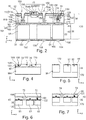
- the figure 1 represents a portion of a system 2 soldered to a printed circuit 4 or PCT (“Printed Circuit Board”) by means of an array 6 of solder balls (in English, “Solder bumps”). To simplify the illustration, only four balls 8 to 11 of the array 6 are shown.
- the system 2 is typically in the form of a parallelepiped housing inside which electronic and optical chips are housed. Only the solder balls of the system 2 protrude on a lower face of this housing. To simplify the illustration, this box has not been shown on the figure 1 .
- System 2 in its case is known by the English name of 'system in package'. More generically, the system 2 is also often referred to by the term “integrated circuit”.
- the horizontal is defined in the figures by X and Y directions of an orthogonal frame of reference R.
- the Z direction of the frame of reference R corresponds to the vertical direction.
- Terms such as “lower”, “upper”, “above”, “below”, “top” and “bottom” are defined with respect to this Z direction.
- system 2 comprises a support 14.
- the balls of the array 6 are placed directly on the underside of the support 14.
- the assembly of the support 14 and of the array 6 is known by the acronym BGA ("Ball Grid Array ”).
- BGA All Grid Array
- the upper face of the support 14 has pads on which chips electronics and / or photonics can be soldered.
- system 2 comprises an electronic chip 16 and a photonic chip 18. These two chips 16 and 18 are both directly welded to the upper face of the support 14.
- the electronic chip only comprises electronic components connected to each other to perform predetermined functions.
- the electronic chip 16 therefore has no optical component.
- the photonic chip 18 has no electronic component.
- the photonic chip 18 and the electronic chip 16 of the system 2 are electrically connected to pads on the upper face of the support 14.
- the chips 16 and 18 are also electrically connected to the printed circuit. 4.
- the chips 16 and 18 are welded to respective pads of the upper face of the support 14 by means of networks, respectively 20 and 22, of solder beads.
- the networks 20 and 22 are represented by some of these solder microspheres located under the chips 16 and 18.
- the solder microbeads are known by the English term of “C4 Bumps”.
- the support 14 comprises electrical connections which extend mainly horizontally, such as a connection 24.
- the connection 24 electrically connects certain pads of the upper face of the support 14 to each other in order to allow the exchange of electrical or power signals. electrical between the chips soldered on these pads.
- the support 14 is also crossed by vertical connections, such as connections 26 and 28.
- these vertical connections lead to a horizontal metal line of a redistribution layer better known by the acronym RDL (“Redistribution layer”). .
- RDL redistribution layer
- the horizontal lines of the redistribution layer electrically connect some of the vertical connections to corresponding solder balls of the network 6.
- the vertical connections make it possible in particular to supply the chips 16 and 18 with electricity and, also, to exchange electrical signals with d 'other chips soldered on the printed circuit 4.
- the support 14 is generally devoid of any other electrical or optical component.
- the layers 36 and 38 are directly bonded to one another at the level of a bonding interface 40 which extends essentially in a horizontal plane.
- the upper face of the layer 38 corresponds to the upper face 32 and the lower face of the layer 36 corresponds to the lower face 34.
- Layer 36 is mainly made of a non-conductive material.
- non-conductive material denotes a material whose conductivity at 20 ° C. is less than 10 -1 or 10 -2 S / m.
- this non-conductive material can be a semiconductor material such as undoped silicon or an electrically insulating material such as glass.
- the non-conductive material is undoped crystalline silicon.
- conductive material or “electrically conductive material” denotes a material whose electrical conductivity at 20 ° C. is generally greater than 10 5 or 10 6 S / m.
- the layer 36 comprises a sublayer 42 of undoped crystalline silicon and a surface sublayer 44 produced directly on the sublayer 42.
- the sublayer 44 is made of silicon dioxide.
- the lower face of the sublayer 42 corresponds to the face 34.
- the thickness of the sublayer 42 is large enough to be rigid enough and not to have too great a deflection. In particular, the thickness of the sublayer 42 is sufficient to make it possible to handle the chip 18. For this purpose, the thickness of the sublayer 42 is greater than 50 ⁇ m or 80 ⁇ m or 100 ⁇ m.
- the sublayer 42 comprises via, called hereinafter “primary via” which make it possible to form electrical connections which vertically pass through the substrate 30.
- Each primary via extends from a lower end to an upper end. The lower end is flush with the lower face 34. The upper end is flush with the bonding interface 40. These primary via therefore pass through the entire thickness of the interconnection layer 36. On the other hand, the primary via do not cross and do not penetrate inside the optical layer 38.
- Layer 36 does not contain a layer of buried silicon oxide. Its minimum thickness giving rise to an acceptable deflection is therefore less than that of a layer which would contain such a layer of buried silicon oxide. Having a lesser thickness makes it possible in particular to reduce the parasitic capacitances of the primary via which is proportional to the height of the primary via. Thus, preferably, the thickness of the sub-layer 42 is also less than 150 ⁇ m or 100 ⁇ m.
- the figure 2 represents only three primary via 50-52. However, in general, layer 36 has a much larger number of primary via. By For example, all the primary via are identical so that subsequently only the primary via 50 is described in more detail.
- the primary via 50 is carried out in a conventional manner.
- the reader can consult the following article: Ken Miyairi et Al: “Full integration and electrical characterization of 3D Silicon Interposer demonstrator incorporating high density TSVs and interconnects”, 45th International Symposium on Microelectronics, 2012 .
- Ken Miyairi et Al “Full integration and electrical characterization of 3D Silicon Interposer demonstrator incorporating high density TSVs and interconnects”
- the lower part 54 extends vertically from the lower end of the via 50 to the upper part 56.
- the horizontal section of the lower part is substantially constant over its entire height. Its height and its diameter are subsequently denoted, respectively, H1 and D1.
- the lower portion 54 passes through at least 80% and preferably at least 90% or 95% of the thickness of the layer 36. Since the thickness of the layer 36 is large, the diameter D1 is also important for whether the aspect ratio H1 / D1 is less than 10/1 or 8/1. Indeed, it is difficult to manufacture via having an aspect ratio greater than 10/1.
- the height H1 is greater than 80% or 90% or 95% of the thickness of the underlayer 42. Under these conditions, the height H1 is between 80 ⁇ m and 142.5 ⁇ m and, generally, between 95 ⁇ m and 130 ⁇ m.
- the diameter D1 is then typically between 10 ⁇ m and 20 ⁇ m.
- metal via denotes a via made of metal and the diameter of which is small, that is to say the diameter of which is less than 3 ⁇ m and, generally, less than 1 ⁇ m.
- the height of a metal via is also small, that is to say less than 3 ⁇ m or 1 ⁇ m.
- the metal is copper.
- the structure of such an interconnection metal network is well known to those skilled in the art. This is the redistribution layer interconnect metal network or RDL.
- the thickness of the sublayer 44 is typically less than 10 ⁇ m or 3 ⁇ m.
- the diameter of the upper part 56 is equal to the largest diameter of a metal via which composes it.
- the diameter of the upper part 56 is therefore less than 10 ⁇ m and generally less than 3 ⁇ m or 1 ⁇ m.
- the optical layer 38 comprises at least one optical component buried inside this layer.
- the optical component is chosen from the group consisting of an optical modulator, a laser source, a waveguide, a photodetector, a demultiplexer and an optical multiplexer. Of the optical components in this group, all are active optical components except the waveguide.
- Component 70 is a laser source and component 72 is an optical modulator.
- the component 72 is capable of modifying, as a function of an electrical control signal, the phase, the amplitude or the intensity of an optical signal which passes through it.
- Such optical modulators are well known so that component 72 is not described here in detail.
- Component 72 comprises an electrical contact 74 intended to receive the electrical control signal.
- this electrical contact 74 is buried inside the optical layer 38.
- the electrical contact 74 is located on a lower face of the component 72. The electrical contact 74 is therefore turned towards the interface 40. lift-off. In this configuration, the electrical contact 74 is only accessible from below the optical component 72.
- Component 70 also includes an upper socket 84 and a lower socket 86 directly in contact, respectively, with the upper 82 and lower 78 layers.
- the active layer 80 generates the optical signal emitted by the component 70 when an appropriate potential difference is applied between the taps 84 and 86.
- the lower layer 78 is optically coupled to the waveguide 76.
- the layer 78 is disposed above the waveguide 76 and separated from this waveguide 76 by a thin sublayer 90 d. buried oxide.
- the thickness of the oxide sublayer 90 is less than 100 nm and, preferably, less than 50 nm or 20 nm.
- the waveguide 76 and the optical component 72 are buried within an encapsulation sublayer 122 located directly below the oxide sublayer 90. More specifically, the sublayer 122 extends from a sublayer 120 up to the sublayer 90. The sublayer 122 is broken down here into an upper level 92 of optical guidance and into a lower level 94 of electrical interconnection. Level 92 includes all the optical components and parts of optical components made under the sublayer 90. Level 92 therefore here includes the waveguide 76, the optical component 72 and a dielectric material in which the optical components and parts of optical components are encapsulated. For example, this level 92 is fabricated from a crystalline silicon sublayer in which the waveguide 76 and component 72 have been fabricated before being encapsulated in the dielectric material.
- Level 94 is devoid of optical component and optical component part.
- level 94 has metal interconnect arrays encapsulated in a dielectric material as will be described later.
- the dielectric material of the sublayer 122 has a refractive index lower than the refractive index of the material used to make the waveguide 76 and the component 72.
- the dielectric material is silicon dioxide.
- the layers 78, 80 and 82 are for their part made in a sublayer 128 located directly on the sublayer 90.
- the sublayer 128 here comprises a III-V material in which the layers 78, 80 and 82 are made. and a dielectric material which encapsulates layers 78, 80 and 82.
- Sublayer 128 extends horizontally directly above sublayer 90 and its upper face corresponds to face 32.
- this layer 38 includes via, called “secondary via”.
- Each secondary via extends a primary via inside the optical layer 38.
- each secondary via extends from the bonding interface 40 towards the inside of the layer 38.
- the diameter of the secondary via is much smaller than the diameter of the primary via.
- the diameter of the secondary via is less than 3 ⁇ m and, preferably, less than 1 ⁇ m.
- the thickness of the layer 38 is less than 15 ⁇ m or or 8 ⁇ m or 5 ⁇ m.
- the secondary via are classified into two categories.
- a first category called “secondary crossing via” and a second category called “secondary non-crossing via”.
- the secondary via through the thickness of the layer 38 and therefore, in particular, the level 92 of optical guidance. They therefore extend vertically from the bonding interface 40 to the upper face 32. They are typically used to electrically connect the electrical tracks formed on the upper face 32 to one of the primary via. Conversely, the non-traversing secondary via do not completely pass through the thickness of the layer 38 and, in particular, do not pass through the level 92 of optical guidance. They therefore extend from the bonding interface 40 to an electrical contact, such as contact 74, buried inside. of layer 38.
- the figure 2 represents two through secondary via 100 and 102.
- the via 100 electrically connects the primary via 50 to an electrical track 106 made on the face 32.
- the track 106 electrically connects the upper end of the via 100 to the socket 84.
- the lower end of via 100 is in direct mechanical and electrical contact with metal line 58.
- the through secondary via 102 electrically connects the primary via 51 to an electrical track 108 made on the face 32.
- the track 108 electrically connects the end of the via 102 to the socket 86.
- the lower end of the via 102 is directly in mechanical contact. and electrical with the metal line from via 51.
- via 100 and 102 are used to power component 70.
- via 102 The structure of via 102 is identical to that of via 100. Thus, only the structure of via 100 is described below in more detail.
- the via 100 has a lower part 110 and an upper part 112 arranged immediately one above the other. Parts 110 and 112 are made, during manufacture, from opposite sides of the optical layer.
- the diameter of the lower part 110 is defined in the same way as for the upper part 58 of the primary via 50.
- the diameter of the part 110 is less than 3 ⁇ m or 1 ⁇ m.
- the interconnecting metal network that forms part 110 has only two levels of metal lines. For example, these are the levels often designated by the references M4 and M5.
- this part 110 is low, that is to say less than 6 ⁇ m or 3 ⁇ m or 1 ⁇ m.
- the metal line 116 is produced in a silicon oxide sublayer 120, the lower face of which coincides with the bonding interface 40.
- the sublayer 120 is produced directly under the sublayer 122.
- the sublayer 120 is made of silicon dioxide.
- Metal via 118 are located inside level 94 of sublayer 122.
- the upper part 112 of the secondary via 100 is formed by a coating 124 of conductive material.
- the coating 124 is made of copper or aluminum.
- This coating 124 continuously covers the vertical walls and the bottom of a hole 126 dug in the layer 38. More precisely, the hole 126 extends from the upper face 32 to the metal line 114. For this, the hole 126 successively passes from the top to the bottom, the encapsulation layer 128, the sublayer 90, the level 92 of optical guidance and a part of the level 94 of the sublayer 122.
- the maximum diameter of hole 126 is less than 3 ⁇ m and, preferably, less than 1 ⁇ m.
- the maximum diameter of the upper part 112 of the secondary via 100 is also less than 3 ⁇ m or 1 ⁇ m.
- the coating 124 is in direct mechanical and electrical contact with the track 106 and, in its lower part, in direct mechanical and electrical contact with the metal line 114.
- the coating 124 does not fill the entire hole 126.
- the center of the hole 126 is therefore hollowed out.
- the thickness of the coating 124 is less than 500 nm or 300 nm.
- the center of hole 126 is filled with an electrically non-conductive and passivating material.
- the coefficient of expansion of this electrically non-conductive material is less than 0.8C 124 , and preferably less than 0.5C 124 or 0.3C 124 , where C 124 is the coefficient of thermal expansion of the coating 124.
- the center of the hole 126 is filled with the same dielectric material as that of the sub-layer 122, that is to say silicon dioxide.
- Layer 38 also includes a non-traversing secondary via 130.
- Via 130 electrically connects electrical contact 74 to the upper end of primary via 52 to receive the electrical control signal from optical component 72.
- via 130 extends vertically from the bonding interface 40 to the electrical contact 74. It therefore completely passes through the sublayer 120 and the level 94 of the sublayer 122. On the other hand, it does not cross the guide level 92 optics or the sublayer 90.
- the via 130 does not open into the upper face 32 unlike a secondary through via.
- the metal line 138 is in direct mechanical and electrical contact on the upper end of the primary via 52.
- the interconnecting metal network has five different levels of metal lines. For example, these five levels of metal lines are often designated by the references, respectively, M1 to M5.
- the diameter of via 130 is also less than 3 ⁇ m or 1 ⁇ m.
- Redistribution lines 150 are made on the underside 34 to connect electrically the lower ends of the primary via to corresponding solder beads. To this end, the redistribution lines include connection pads to which the solder microspheres are directly fixed. On the figure 1 , only three solder beads 152 to 154 are shown. These microbeads 152 to 154 are intended to be welded to corresponding pads on the upper face of the support 14 and therefore form part of the network 22 of welding microbeads.
- the lines 150 are buried inside an encapsulation layer 156 made of an electrically non-conductive material such as a polymer.
- the stack of sublayers 90, 122 and 120 is manufactured on a handle 164 ( figure 4 ) then provided.
- this stack constitutes only a part of the optical layer because it lacks, at this stage, in particular, the layer 128.
- the sublayer 120 is located on the side opposite the handle 164 and has a face 166 of collage. This face 166 is suitable for being bonded to another substrate by direct bonding, that is to say by bonding which does not require the addition of material.
- the underlayer 90 is directly attached to the handle 164.
- the handle 164 is a support which allows easy handling of the stack of the underlayer 120, 122 and 90.
- the thickness of the handle 164 is typically greater than 250 ⁇ m or 500 ⁇ m.
- the handle 164 is a silicon substrate with a thickness of 750 ⁇ m or 775 ⁇ m.
- the sublayer 90 is the buried oxide layer of a substrate known by the acronym SOI (“Silicon On Insulator”).
- SOI Silicon On Insulator
- the waveguide 76 and the component 72 are produced, typically by etching, in the monocrystalline silicon layer of this SOI substrate.
- the waveguide 76 and the optical component 72 are buried in the dielectric material of the sublayer 122 by successively depositing several layers of oxide one after the other. others.
- the interconnecting metal networks forming the secondary via 130 and the lower parts 110 of the secondary via 100 and 102 are produced.
- these interconnecting metal networks are made from the side opposite to the handle 164.
- the methods of making the optical components on the sublayer 90, the methods of burying components inside the sublayer. layer 122 and the methods of making interconnecting metal networks are well known and are therefore not described in more detail here. Note that at this stage of the manufacturing process, the production of the upper parts 112 of the secondary via 100 and 102 is impossible. The sublayer 122 therefore does not include, at this stage, the upper parts 112 of the via 100 and 102.
- the interconnection layer 36 is fabricated on a handle 170 ( figure 5 ) then provided.
- the layer 36 has an outer face 172 located on the side opposite to the handle 170.
- This face 172 is a bonding face, that is to say capable of being bonded, by direct bonding, to the face 166.
- the thickness of the handle 170 is greater than 250 ⁇ m or 500 ⁇ m to allow easy handling of the layer 36.
- the handle 170 is for example a silicon substrate.
- Step 162 also comprises the production of primary via 50 to 52 in the layer 36.
- the layer 36 comprises these primary via 50 to 52.
- the production of such a layer 36 on the handle 170 and the realization of the via 50 to 52 in this layer 36 are conventional.
- parts 54 of vias 50 to 52 consist of a coating of dielectric material, covered with a barrier layer of titanium or tantalum, and filled with copper. A method of manufacturing these parts 54 is for example described in the article by Ken Miyairi cited above.
- the metal via 60 are made, in electrical contact with the parts 54 of the primary via.
- the metal lines, such as the metal line 58 are produced and then encapsulated in the sublayer 44 of oxide. The outer face of the sublayer 44 is then prepared for its direct bonding to the face 166.
- the faces 166 and 172 are glued, by direct gluing, one on the other. This is shown on the figure 6 .
- the bonding interface 40 is then obtained.
- it is a direct hybrid copper-oxide bond as described in the following article: Yan Beillard et Al: “Chip to wafer copper direct bonding electrical characterization and thermal cycling”, 3D Systems Integration Conference (3DIC), 2013 IEEE International .
- handle 164 is removed to expose the underlayer 90 ( figure 7 ).
- handle 164 is removed by mechanical and chemical polishing known by the acronym CMP ("Chemical Mechanical Polishing"), followed by selective chemical etching.
- CMP Chemical Mechanical Polishing
- the light amplifying part of the component 70 is produced on the sub-layer 90, on the side opposite to the optical guidance level 92 ( figure 8 ) and encapsulated in the dielectric material of the encapsulation layer 128.
- the sockets 84, 86, the electrical tracks 106 and 108 and the upper parts 112 of the secondary via 100 and 102 are produced ( figure 9 ).
- holes such as hole 126 are first dug through sublayers 128, 90 and level 92 of sublayer 122.
- a coating of conductive material is deposited over the entire exterior face.
- this conductive coating is etched so that the conductive coating only remains locations of the taps 84, 86, of the tracks 106 and 108 and of the upper parts 112 of the secondary via 100 and 102.
- the production of the layer 38 is then finished.
- the handle 170 is then withdrawn in turn to expose the lower face 34 ( figure 10 ).
- the redistribution lines 150, the solder microbeads 152 to 154 and the encapsulation layer 156 are produced on the lower face 34 exposed. The manufacture of the photonic chip 18 is then completed.
- the electronic chip 16 and the photonic chip 18 are welded to pads on the upper face of the support 14.
- the chips 16 and 18 are then electrically connected to each other via the horizontal connections of the support 14.
- the support 14 and the chips 16 and 18 are encapsulated in an electrically non-conductive material and a good thermal conductor, such as an epoxy resin.
- a cover on which is disposed a heat sink, such as a heat sink is fixed to the upper faces of the chips 16 and 18.
- This cover is for example glued, using a thermally glue.
- conductive directly on the upper face 32 of the photonic chip 18 and the upper face of the chip 16.
- these upper faces can be directly in contact with the thermal adhesive which is in contact with the cover. This is made possible by the fact that all electrical signals and power supplies are brought through the undersides of chips 16 and 18.
- the system 2 is for example soldered to the printed circuit 4.
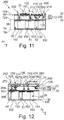
- the optical layer 202 is identical to the optical layer 38 except that it additionally comprises an active electronic component 210 buried inside the level 92 of the sublayer 122.
- This electronic component 210 is qualified as active because, for to function, it needs to be supplied with electricity, and it emits and / or receives an electric signal.
- the component 210 comprises an electrical contact 212 on its lower face. This electrical contact 212 is therefore buried inside the sublayer 122 and turned towards the bonding interface 40.
- the secondary via 204 electrically connects the electrical contact 212 of the electronic component 210 to the primary via 52 by crossing only the lower level 94 of the sublayer 122 and the sublayer 120.
- the electronic component 210 is, for example, intended for in supplying, from an electrical signal which it receives via the primary via 52, an electrical control signal to the optical component 72.
- the component 210 comprises on its lower face another electrical contact connected to the contact 74 of the component 72.
- the interconnection metal network located inside the level 94 of the sublayer 122 is modified to create a path which electrically connects together this other electrical contact and the contact 74. To simplify the figure 11 , this modification of the metal interconnection network has not been shown on the figure 11 .
- the structure and manufacture of via 204 can be deduced from the explanations given for via 130.
- Via 206 is a via which electrically connects a metal line 135, buried within level 94 of sublayer 122, to an electrical track 216 made on the upper face 32. Via 206 extends vertically from the face 32 up to the line 135 of buried metal, crossing in particular the sublayer 90 and the level 92 of optical guidance.
- the electrical track 216 comprises a test pad which makes it possible to test the correct operation of the components 210 and / or 72 during the manufacturing process of the photonic chip 200 and, in particular, before the removal of the handle 170.
- the interconnecting metal network located inside level 94 of sublayer 122, is also modified to create, using metal lines and metal via, an electrical path that electrically connects the electrical contacts 212 and / or 74 to the metal line 135.
- via 206 is here identical to that of via 100 except that it does not have a lower part 110.
- via 206 is manufactured in the same way as the upper part 112 of via 100 and generally at the same time as this. upper part 112.
- the through secondary via 252 and 254 are identical, respectively, to via 100 and 102 except that their upper part 270 is made differently. More precisely, the upper part 270 is here a solid via. In other words, the upper part 270 is identical to the upper part 112, except that the central recess of the hole 126 is filled with a conductive material. Generally, in this case, the maximum diameter of the upper part 270 of the via 252 and 254 is less than 1 ⁇ m.
- the laser source 256 is identical to the component 70, except that the socket 86 is replaced by a socket 274.
- the socket 274 is a metallic via which electrically connects the layer 78 to the electrical track 108.
- the underside of the waveguide 76 of the laser source 256 also has an electrical contact 264.
- This electrical contact 264 is connected thermally to the interconnect layer 36 through a non-traversing via 266.
- Via 266 is structurally identical, for example, to via 130. However, unlike via 130, via 266 does not necessarily have to be function of electrically connecting the contact 264 to a primary via of the layer 36.
- the lower end of the via 264 is directly in mechanical and electrical contact with a metal line, located inside the sublayer 44, which is flush with interface 40. This metal line is here electrically isolated from all the primary via.
- Via 266 is here made of a material which is a good thermal conductor.
- a “good thermal conductor” material is typically a material whose thermal conductivity is greater than 1.2C 122 , and preferably greater than 2C 122 or 3C 122 , where C 122 is the thermal conductivity of the dielectric material of the sublayer 122.
- the material used to make via 266 is the same as that used to make via 130.
- the presence of via 266 improves the thermal dissipation of the heat produced by laser source 256. Indeed, it is known to the industry. those skilled in the art that the waveguide 76 sees its temperature increase during the operation of the laser source 256. In the absence of the via 266, the presence of the dielectric material of the sublayer 122 under the waveguide 76 does not does not effectively evacuate the heat produced.
- the via 266 produces a thermal bridge, here made of metal, through the sub-layer 122 which thermally connects the waveguide 76 to the layer 36. This makes it possible to more efficiently remove the heat produced by the laser source 256.
- the through secondary via 258 electrically and directly connects the primary via 52 to an electrical track 276 produced on the upper face 32.
- the track 276 comprises a pad on which is welded a first electrical contact of the electronic chip 260.
- the structure of the via 258 is here identical to that of via 252.
- the via 262 electrically connects directly an electrical track 280 made on the upper face 32 to the metal line 135 buried inside the level 94 of the sublayer 122.
- the structure of via 262 is identical to the structure of via 252 except that the lower part 110 is omitted.
- the electrical track 280 comprises a pad on which is welded a second electrical contact of the electronic chip 260.
- metal line 135 is electrically connected to the electrical contact 74 of the optical component 72 via an interconnecting metal network similar to that described with reference to figure 11 .
- electronic chip 260 is a transducer, electrically powered by primary via, which controls optical component 72 based on electrical signals received via primary via, e.g., 52.
- the horizontal cross section of a via is not necessarily circular.
- the cross section of a via can be square or rectangular.
- the term “diameter” denotes the hydraulic diameter of this horizontal cross section.
- the diameter of the via is not necessarily constant over its entire height.
- the term “diameter” of the via denotes the largest diameter of this via along its height.
- the upper portion 56 of the primary via is omitted.
- the upper end of part 54 of the primary via is directly flush with the bonding interface 40.
- the metal via 60 are omitted.
- the upper end of the part 54 is in direct mechanical and electrical contact with the metal line 58.
- the upper part 56 of a primary via may include several additional lines of metal made at different depths inside the sublayer 44.
- the different levels of metal lines of the part 56 are then electrically connected to each other by metal via.
- These additional metal lines then form a redistribution layer or RDL which makes it possible, for example, to electrically connect together several metal lines which are flush with the interface 40.
- the interconnecting metal network used to form the lower portion of a secondary through via may also, alternatively, have more than three levels of metal lines.
- a secondary through via is omitted.
- the bottom of the hole 126 then opens directly onto the metal line 58 of the primary via.
- Such a secondary crossing via then has only one part, namely part 112.
- the center of the hole 126 can also be filled with a dielectric material different from the dielectric material of the sublayer 122.
- a dielectric material different from the dielectric material of the sublayer 122.
- it is filled with an organic material.
- the interconnection layer 36 can be made from materials other than silicon.
- it is made of glass.
- layer 36 comprises one or more electronic components.
- the sublayers of optical layer 38 can also be made from other materials.
- the sublayer 122 can be produced using another dielectric material such as, for example, amorphous silicon, silicon nitride SiN or silicon nitride oxide SiON.
- the different oxide sublayers of layer 38 are not necessarily all made from the same oxide.
- the sublayer 120 is produced in an oxide different from that used to produce the sublayer 90. It is also possible to use an oxide to produce the sublayer 122 which is different from that of the sublayer. layer 90.
- the optical layer can also be crossed by additional via whose diameter is greater than 3 ⁇ m and, for example, greater than 10 ⁇ m or 20 ⁇ m.
- additional via whose diameter is greater than 3 ⁇ m and, for example, greater than 10 ⁇ m or 20 ⁇ m.
- a large surface exclusion zone is provided around each of these additional via and no optical component is made inside this exclusion zone.
- This exclusion zone is sized in accordance with the teaching given in the previously cited Yang2013 article.
- the photonic chip includes some of these additional via, the implantation of the optical components in the optical layer is still simplified because of the presence of secondary via which nevertheless limits the constraints on the placement of the optical components. .
- the number of optical components buried within level 92 of sublayer 122 can be any.
- the various optical components are not necessarily buried inside level 92 at the same depth. This is especially the case if the optical components or parts of optical components are made from different sub-layers of material stacked on top of each other. These material sub-layers can then be chosen from the group consisting of a crystalline silicon sub-layer, an amorphous silicon sub-layer, a silicon nitride sub-layer SiN and a sub-layer. -silicon nitride oxide layer SiON.
- component 70 or laser source 256 is omitted.
- the encapsulation layer 128 can also be omitted so that the upper face 32 then corresponds to the upper face of the sublayer 90.
- the lower end of secondary via 266 is electrically and mechanically connected to at least one primary via.
- This primary via is then not necessarily used to establish an electrical connection but above all to improve the thermal dissipation of the heat produced by the laser source.
- the diameter of via 266 is not necessarily less than 3 ⁇ m or 1 ⁇ m. Its diameter can also be greater than these values.
- via 266 to improve the dissipation of the heat produced by a laser source is similarly applicable to the improvement of the heat produced by any type of optical or electronic component of which at least a part is buried in the interior of sublayer 122.
- a via similar to via 266 can also be used to dissipate the heat produced by optical component 72 or electronic component 210.
- the photonic chip may include an electrical track produced on the upper face 32 which is not necessarily used to electrically connect an optical component to one of the primary via.
- an electrical track 276 can only be used to electrically connect an electronic chip soldered on the upper face 32 of the photonic chip to one of the primary via.
- the photonic chip only comprises non-traversing secondary via.
- all of the non-through secondary via are made from the side opposite to the handle 164.
- the handle removal order can then be reversed.
- the handle 170 can be removed before the handle 164.
- the non-crossing secondary via is entirely manufactured before the bonding of the layer 38 on the layer 36.
- the photonic chip has only secondary through vias.
- chip 260 can correspond to chip 16 of the figure 1 .
- the electronic chip 260 is an ASIC supplied electrically by means of the primary via, and which controls the optical component 72 with the electric signals which it generates.
- thermally connecting a part of the component 70 or of the laser source 256 to the interconnection layer via secondary, typically non-traversing via, such as via 266, can be implemented independently of the other characteristics described. here of the photonic chip. In particular, this can be implemented in a context where the primary via passes through the optical layer as described in the article Yang2013 or in a context where all the primary via are omitted.
- the primary via do not generate substantial mechanical stress on the optical components.
- the interconnection layer 36 is totally devoid of optical component. These are only located inside the diaper. Therefore, the optical components can be implanted with respect to each other without worrying about the arrangement of the primary via. In particular, it is not necessary to respect any exclusion zone around each primary via.
- the secondary via passing through the optical guidance level 92 have a diameter preferably less than or equal to 3 ⁇ m, or even 1 ⁇ m. Such secondary through vias can thus be placed 4 ⁇ m or even 2 ⁇ m away from the optical components without generating mechanical stresses on the latter.
- the through vias described in Yang2013 must be placed 40 ⁇ m from the optical components so as not to constrain them mechanically. It is therefore possible to place the optical components much closer to the secondary via than what would have been possible if their diameter had been equal to the diameter of the primary via.
- the combination in the same photonic chip of primary via and secondary via therefore makes it possible to obtain a sufficiently thick photonic chip to have an acceptable deflection while limiting the constraints to be observed in order to place the optical components with respect to the via.
- the interconnection layer does not necessarily contain a layer of buried silicon oxide. Its minimum thickness giving rise to an acceptable deflection is therefore less than that of a layer which would contain a buried silicon oxide. Having a lesser thickness of the interconnection layer makes it possible in particular to reduce the parasitic capacitances of the primary via. Indeed, this parasitic capacity is proportional to the height of the primary via.
- the fact of placing the laser source on the upper face of the oxide layer 90 facilitates its cooling from the outside, in particular thanks to the casing of the system.
- the center of the hole 126 is filled with an electrically non-conductive material whose coefficient of thermal expansion is smaller than that of the coating 124 makes it possible to further limit the mechanical stresses exerted by the secondary via on the optical components located near.
Description
L'invention concerne une puce photonique traversée par un via ainsi qu'un procédé de fabrication d'une telle puce photonique.The invention relates to a photonic chip through which a via passes and to a method of manufacturing such a photonic chip.
Un via est une connexion électrique verticale, c'est-à-dire qui s'étend principalement dans une direction perpendiculaire au plan de la puce photonique.A via is a vertical electrical connection, that is, one that extends mainly in a direction perpendicular to the plane of the photonic chip.
Les puces photoniques s'étendent essentiellement dans un plan appelé par la suite « plan de la puce ».Photonic chips extend essentially in a plane called hereinafter "the plane of the chip".
Les puces photoniques connues comportent :
- un substrat présentant des faces supérieure et inférieure parallèles au plan de la puce, ce substrat comportant, entre les faces supérieure et inférieure :
- une couche d'interconnexion d'épaisseur supérieure à 50 µm, cette couche d'interconnexion étant dépourvue de composant optique,
- une couche optique collée, au niveau d'une interface de collage, sur la couche d'interconnexion,
- au moins un composant optique enterré à l'intérieur de la couche optique,
- une borne électrique choisie dans le groupe constitué d'un contact électrique enfoui à l'intérieur de la couche optique, ce contact électrique enfoui étant celui du composant optique ou d'un composant électronique, et d'une piste électrique réalisée sur la face supérieure du substrat,
- des plots de raccordement électrique réalisés sur la face inférieure du substrat, chacun de ces plots étant apte à être connecté électriquement par l'intermédiaire d'une bille de soudure à un autre support,
- un via primaire s'étendant à travers la couche d'interconnexion depuis la face inférieure pour raccorder électriquement l'un des plots de raccordement à la borne électrique, ce via primaire ayant un diamètre supérieur ou égal à 10 µm.
- a substrate having upper and lower faces parallel to the plane of the chip, this substrate comprising, between the upper and lower faces:
- an interconnection layer with a thickness greater than 50 μm, this interconnection layer being devoid of optical component,
- an optical layer bonded, at a bonding interface, to the interconnection layer,
- at least one optical component buried inside the optical layer,
- an electrical terminal chosen from the group consisting of an electrical contact buried inside the optical layer, this buried electrical contact being that of the optical component or of an electronic component, and of an electrical track made on the upper face the substrate,
- electrical connection pads made on the underside of the substrate, each of these pads being able to be electrically connected by means of a solder ball to another support,
- a primary via extending through the interconnection layer from the underside to electrically connect one of the connection pads to the electrical terminal, this primary via having a diameter greater than or equal to 10 μm.
Une telle puce photonique est par exemple décrite dans l'article suivant :
Il est connu que la présence de via traversants à proximité d'un composant optique pose des problèmes. En effet, de tels via sont réalisés dans un matériau électriquement conducteur, dont le coefficient de dilatation thermique est différent du matériau dans lequel est réalisé le composant optique. Ainsi, en réponse à des variations de température, les via exercent sur le composant optique situé à proximité une contrainte mécanique qui varie en fonction de la température. Cette variation de la contrainte mécanique modifie les propriétés optiques du composant optique et entraîne une modification des propriétés de ce composant optique. Par exemple, lorsque le composant optique est un filtre optique, cela modifie sa longueur d'onde centrale. De telles variations des propriétés du composant optique doivent être évitées.It is known that the presence of through via near an optical component poses problems. Indeed, such via are made of an electrically conductive material, the coefficient of thermal expansion of which is different from the material in which the optical component is made. Thus, in response to variations in temperature, the via exert on the optical component located nearby a mechanical stress which varies as a function of the temperature. This variation of the mechanical stress modifies the optical properties of the optical component and causes a modification of the properties of this optical component. For example, when the optical component is an optical filter, this changes its central wavelength. Such variations in the properties of the optical component should be avoided.
Pour cela, l'article Yang2013 propose d'éloigner les via traversants des composants optiques. Plus précisément, il propose de définir une zone d'exclusion autour de chaque via. A l'intérieur de chaque zone d'exclusion, aucun composant optique ne doit être implanté. Il a été démontré que cette zone d'exclusion est d'autant plus grande que le diamètre du via traversant est important.For this, the Yang2013 article proposes to move the through-through via away from optical components. More precisely, he proposes to define an exclusion zone around each via. Within each exclusion zone, no optical component should be implanted. It has been shown that this exclusion zone is all the larger the larger the diameter of the through via.
Par ailleurs, une puce photonique doit avoir une épaisseur suffisamment importante pour être assez rigide et ne pas présenter une flèche trop importante. Or, les procédés de fabrication des via traversants génèrent des limitations sur l'épaisseur de la puce photonique. Typiquement, les puces comprenant des via traversants ont une épaisseur supérieure à 50 µm ou 100 µm. Il a par ailleurs été montré, dans le cas des substrats SOI (« Silicon On Insulator »), que des via traversants une couche d'oxyde enterrée, engendrent une flèche plus importante que lorsque ces via sont réalisés dans un substrat de même épaisseur mais dépourvu d'une telle couche d'oxyde enterrée. Ainsi, afin de ne pas présenter une flèche trop importante, si l'épaisseur minimale pour une puce avec via formés dans un substrat en silicium est de 100 µm, cette épaisseur doit être typiquement d'au moins 150 µm pour une puce avec via formés dans un substrat SOI.Furthermore, a photonic chip must have a sufficiently large thickness to be rigid enough and not to have too great a deflection. However, the through-via manufacturing processes generate limitations on the thickness of the photonic chip. Typically, the chips comprising through vias have a thickness greater than 50 μm or 100 μm. It has also been shown, in the case of SOI (“Silicon On Insulator”) substrates, that via passing through a buried oxide layer, generate a greater deflection than when these via are produced in a substrate of the same thickness but devoid of such a buried oxide layer. Thus, in order not to present an excessively large arrow, if the minimum thickness for a chip with via formed in a silicon substrate is 100 μm, this thickness must typically be at least 150 μm for a chip with via formed in an SOI substrate.
Généralement, plus un via doit traverser un substrat d'épaisseur importante, plus son diamètre est important. Typiquement, il est possible de fabriquer des via de facteur de forme « hauteur sur diamètre» de 8 pour 1 (noté 8/1 par la suite), voire 10 pour 1 mais très difficilement de facteur de forme supérieur à 10 pour 1. Ainsi, à ce jour, dans les puces photoniques existantes, la hauteur et le diamètre des via traversants la puce photonique et en particulier, traversant un niveau de guidage optique contenant des composants optiques, sont importants. Actuellement, la hauteur et le diamètre de ces via doivent typiquement être supérieurs, respectivement, à 100 µm et à 10 µm voire supérieurs, respectivement, à 150µm et à 20 µm. Par conséquent, la surface des zones d'exclusion est grande. Or, plus la surface des zones d'exclusion est grande, plus cela augmente les contraintes à respecter pour le placement des composants optiques. Cela rend donc plus difficile la conception et la fabrication de telles puces photoniques. Cela augmente également la taille de telles puces photoniques du fait de l'existence de ces zones d'exclusion.Generally, the more a via must pass through a substrate of great thickness, the greater its diameter. Typically, it is possible to manufacture vias with a "height on diameter" form factor of 8 to 1 (noted 8/1 hereinafter), or even 10 to 1 but very difficult to have a form factor greater than 10 to 1. Thus , to date, in existing photonic chips, the height and diameter of the via passing through the photonic chip and in particular, passing through an optical guidance level containing optical components, are important. Currently, the height and the diameter of these via must typically be greater than, respectively, 100 μm and 10 μm or even greater, respectively, than 150 μm and 20 μm. Therefore, the area of exclusion zones is large. Now, the larger the surface of the exclusion zones, the more this increases the constraints to be observed for the placement of the optical components. This therefore makes the design and manufacture of such photonic chips more difficult. It also increases the size of such photonic chips due to the existence of these exclusion zones.
Par ailleurs de l'état de la technique est connu de
L'invention vise à simplifier la conception et la fabrication de ces puces photoniques en proposant une structure de puce photonique qui permet de relâcher les contraintes à respecter pour le placement des composants optiques.The invention aims to simplify the design and manufacture of these photonic chips by proposing a photonic chip structure which makes it possible to relax the constraints to be observed for the placement of the optical components.
Elle a donc pour objet une puce photonique conforme à la revendication 1.It therefore relates to a photonic chip according to claim 1.
Les modes de réalisation de cette puce photonique peuvent comporter une ou plusieurs des caractéristiques des revendications dépendantes.Embodiments of this photonic chip may include one or more of the features of the dependent claims.
L'invention a également pour objet un procédé de fabrication de la puce photonique, objet de la présente demande.The subject of the invention is also a method for manufacturing the photonic chip, which is the subject of the present application.
Les modes de réalisation de ce procédé de fabrication peuvent comporter une ou plusieurs des caractéristiques des revendications dépendantes.The embodiments of this manufacturing process may include one or more of the features of the dependent claims.
L'invention sera mieux comprise à la lecture de la description qui va suivre. Elle est donnée uniquement à titre d'exemple non limitatif tout en se référant aux dessins sur lesquels :
- la
figure 1 est une illustration schématique d'un système comportant une puce photonique ; - la
figure 2 est une illustration schématique, en coupe verticale, de la puce photonique du système de lafigure 1 ; - la
figure 3 est un organigramme d'un procédé de fabrication du système de lafigure 1 ; - les
figures 4 à 10 sont des illustrations schématiques, en coupe verticale, de différents états de fabrication de la puce photonique de lafigure 2 ; - la
figure 11 est une illustration schématique, en coupe verticale, d'une première variante de la puce photonique de lafigure 2 ; - la
figure 12 est une illustration schématique, en coupe verticale, d'une deuxième variante de la puce photonique de lafigure 2 .
- the
figure 1 is a schematic illustration of a system including a photonic chip; - the
figure 2 is a schematic illustration, in vertical section, of the photonic chip of the system of thefigure 1 ; - the
figure 3 is a flowchart of a manufacturing process for the system of thefigure 1 ; - the
figures 4 to 10 are schematic illustrations, in vertical section, of different states of manufacture of the photonic chip of thefigure 2 ; - the
figure 11 is a schematic illustration, in vertical section, of a first variant of the photonic chip of thefigure 2 ; - the
figure 12 is a schematic illustration, in vertical section, of a second variant of the photonic chip of thefigure 2 .
La
Le système 2 se présente typiquement sous la forme d'un boîtier parallélépipédique à l'intérieur duquel sont logés des puces électroniques et optiques. Seules les billes de soudure du système 2 font saillie sur une face inférieure de ce boîtier. Pour simplifier l'illustration, ce boîtier n'a pas été représenté sur la
Dans la suite de cette description, l'horizontal est défini sur les figures par des directions X et Y d'un repère orthogonal R. La direction Z du repère R correspond à la direction verticale. Les termes tels que « inférieur », « supérieur », « dessus », « dessous », « haut » et « bas » sont définis par rapport à cette direction Z.In the remainder of this description, the horizontal is defined in the figures by X and Y directions of an orthogonal frame of reference R. The Z direction of the frame of reference R corresponds to the vertical direction. Terms such as "lower", "upper", "above", "below", "top" and "bottom" are defined with respect to this Z direction.
Dans sa partie inférieure, le système 2 comporte un support 14. Les billes du réseau 6 sont placées directement sur la face inférieure du support 14. L'ensemble du support 14 et du réseau 6 est connu sous l'acronyme BGA (« Ball Grid Array »). La face supérieure du support 14 comporte des plots sur lesquels des puces électroniques et/ou photoniques peuvent être soudées. Dans le cas particulier de la
La puce électronique comporte uniquement des composants électroniques raccordés les uns aux autres pour réaliser des fonctions prédéterminées. La puce électronique 16 est donc dépourvue de composant optique.The electronic chip only comprises electronic components connected to each other to perform predetermined functions. The
A l'inverse, la puce photonique 18 comporte des composants optiques pour remplir des fonctions prédéterminées. Un composant optique est un composant qui, au cours de son utilisation, génère ou modifie ou guide un signal optique. Typiquement, la longueur d'onde λ du signal optique est comprise entre 1200 nm et 1700 nm. Généralement, au moins un de ces composants optiques est un composant optique actif, c'est-à-dire un composant optique :
- qui doit être alimenté par un courant ou une tension électrique pour fonctionner correctement, et/ou
- qui convertit un signal optique en un signal électrique (cas d'un photo-détecteur), ou convertit un signal électrique en un signal optique (cas d'un modulateur de lumière).
- which must be supplied by an electric current or voltage to function properly, and / or
- which converts an optical signal into an electrical signal (case of a photo-detector), or converts an electrical signal into an optical signal (case of a light modulator).
Dans ce mode de réalisation, la puce photonique 18 est dépourvue de composant électronique.In this embodiment, the
Pour être alimentées en électricité ou pour échanger des signaux électriques, la puce photonique 18 et la puce électronique 16 du système 2 sont électriquement raccordées à des plots de la face supérieure du support 14. Les puces 16 et 18 sont également raccordées électriquement au circuit imprimé 4. A cet effet, ici, les puces 16 et 18 sont soudées sur des plots respectifs de la face supérieure du support 14 par l'intermédiaire de réseaux, respectivement 20 et 22, de microbilles de soudure. Sur la
Le support 14 comporte des connexions électriques qui s'étendent principalement horizontalement, telle qu'une connexion 24. La connexion 24 relie électriquement certains plots de la face supérieure du support 14 entre eux afin de permettre l'échange de signaux électriques ou d'alimentation électrique entre les puces soudées sur ces plots. Le support 14 est aussi traversé par des connexions verticales, telles que des connexions 26 et 28. Généralement, ces connexions verticales débouchent sur une ligne de métal horizontale d'une couche de redistribution plus connue sous l'acronyme RDL (« Redistribution layer »). Ici, une seule ligne 25 de cette couche de redistribution est illustrée. Les lignes horizontales de la couche de redistribution relient électriquement certaines des connexions verticales à des billes de soudure correspondantes du réseau 6. Les connexions verticales permettent notamment d'alimenter électriquement les puces 16 et 18 et, aussi, d'échanger des signaux électriques avec d'autres puces soudées sur le circuit imprimé 4. En dehors des connexions horizontales et verticales, le support 14 est généralement dépourvu de tout autre composant électrique ou optique.The
La
- une couche 36 d'interconnexion, et
- une couche optique 38.
- an
interconnection layer 36, and - an
optical layer 38.
Plus précisément, les couches 36 et 38 sont directement collées l'une sur l'autre au niveau d'une interface 40 de collage qui s'étend essentiellement dans un plan horizontal. La face supérieure de la couche 38 correspond à la face supérieure 32 et la face inférieure de la couche 36 correspond à la face inférieure 34.More precisely, the
La couche 36 est principalement réalisée dans un matériau non-conducteur. Dans cette description, on désigne par « matériau non-conducteur » un matériau dont la conductivité à 20°C est inférieure à 10-1 ou 10-2 S/m. Ainsi, ce matériau non-conducteur peut être un matériau semi-conducteur tel que le silicium non dopé ou un matériau électriquement isolant tel que le verre. Ici, le matériau non-conducteur est du silicium cristallin non dopé. A l'inverse, dans cette description, on désigne par « matériau conducteur » ou « matériau électriquement conducteur » un matériau dont la conductivité électrique à 20°C est généralement supérieure à 105 ou 106 S/m.
Ici, la couche 36 comporte une sous-couche 42 en silicium cristallin non dopé et une sous-couche superficielle 44 réalisée directement sur la sous-couche 42. Ici la sous-couche 44 est réalisée en dioxyde de silicium.Here, the
La face inférieure de la sous-couche 42 correspond à la face 34. L'épaisseur de la sous-couche 42 est assez importante pour être assez rigide et ne pas présenter une flèche trop importante. En particulier, l'épaisseur de la sous-couche 42 est suffisante pour permettre de manipuler la puce 18. A cet effet, l'épaisseur de la sous-couche 42 est supérieure à 50 µm ou à 80 µm ou à 100 µm. La sous-couche 42 comporte des via, appelés par la suite « via primaires » qui permettent de former des connexions électriques qui traversent verticalement le substrat 30. Chaque via primaire s'étend depuis une extrémité inférieure jusqu'à une extrémité supérieure. L'extrémité inférieure affleure la face inférieure 34. L'extrémité supérieure affleure l'interface 40 de collage. Ces via primaires traversent donc la totalité de l'épaisseur de la couche 36 d'interconnexion. Par contre, les via primaires ne traversent pas et ne pénètrent pas à l'intérieur de la couche optique 38.The lower face of the
La couche 36 ne contient pas de couche d'oxyde de silicium enterré. Son épaisseur minimale donnant lieu à une flèche acceptable est donc moindre que celle d'une couche qui contiendrait une telle couche d'oxyde de silicium enterré. Avoir une épaisseur moindre permet notamment de diminuer les capacités parasites des via primaires qui est proportionnelle à la hauteur des via primaires. Ainsi, de préférence, l'épaisseur de la sous-couche 42 est également inférieure à 150 µm ou 100 µm.
La
Le via primaire 50 est réalisé de façon conventionnelle. Par exemple, à ce sujet, le lecteur peut consulter l'article suivant :
Dans ce mode de réalisation, le via 50 est formé, en allant du bas vers le haut :
- d'une partie inférieure 54 en forme de barreau vertical, et
- d'une partie supérieure 56 en forme de réseau de métal d'interconnexion.
- a
lower part 54 in the form of a vertical bar, and - an
upper part 56 in the form of an interconnection metal network.
La partie inférieure 54 s'étend verticalement de l'extrémité inférieure du via 50 jusqu'à la partie supérieure 56. La section horizontale de la partie inférieure est sensiblement constante sur toute sa hauteur. Sa hauteur et son diamètre sont par la suite notés, respectivement, H1 et D1. La partie inférieure 54 traverse au moins 80 % et, de préférence, au moins 90 % ou 95 % de l'épaisseur de la couche 36. Étant donné que l'épaisseur de la couche 36 est importante, le diamètre D1 est également important pour que le rapport de forme H1/D1 soit inférieur à 10/1 ou 8/1. En effet, il est difficile de fabriquer des via ayant un rapport de forme supérieur à 10/1. Ici, la hauteur H1 est supérieure à 80 % ou 90 % ou 95 % de l'épaisseur de la sous-couche 42. Dans ces conditions, la hauteur H1 est comprise entre 80 µm et 142,5 µm et, généralement, comprise entre 95 µm et 130 µm. Le diamètre D1 est alors typiquement compris entre 10 µm et 20 µm.The
La partie supérieure 56 du via 50 est formée par un réseau de métal d'interconnexion. Cette partie supérieure 56 se compose donc :
- de lignes de métal qui s'étendent principalement horizontalement, et
- de via métalliques qui raccordent électriquement entre elles ces lignes de métal.
- lines of metal that extend mainly horizontally, and
- of metallic via which electrically connect these metal lines to each other.
Les lignes de métal sont réalisées dans la sous-couche 44 d'oxyde de silicium. Ici, la partie supérieure 56 comporte :
- une ligne de métal 58 qui affleure l'interface 40 de collage, et
- des via métalliques 60 qui raccordent cette ligne 58 directement au sommet de la partie inférieure 54.
- a line of
metal 58 which is flush with thebonding interface 40, and - metal via 60 which connects this
line 58 directly to the top of thelower part 54.
Dans cette description, par « via métallique », on désigne un via réalisé en métal et dont le diamètre est petit, c'est-à-dire dont le diamètre est inférieur à 3 µm et, généralement, inférieur à 1 µm. La hauteur d'un via métallique est également petite, c'est-à-dire inférieure à 3 µm ou 1 µm.In this description, the term “metallic via” denotes a via made of metal and the diameter of which is small, that is to say the diameter of which is less than 3 μm and, generally, less than 1 μm. The height of a metal via is also small, that is to say less than 3 µm or 1 µm.
Ici, le métal est du cuivre. La structure d'un tel réseau de métal d'interconnexion est bien connue de l'homme du métier. Il s'agit de réseau de métal d'interconnexion de la couche de redistribution ou RDL.Here the metal is copper. The structure of such an interconnection metal network is well known to those skilled in the art. This is the redistribution layer interconnect metal network or RDL.
L'épaisseur de la sous-couche 44 est typiquement inférieure à 10 µm ou 3 µm.The thickness of the
Le diamètre de la partie supérieure 56 est égal au plus grand diamètre d'un via métallique qui la compose. Ici, le diamètre de la partie supérieure 56 est donc inférieur à 10 µm et, généralement, inférieur à 3 µm ou à 1 µm.The diameter of the
La couche optique 38 comporte au moins un composant optique enterré à l'intérieur de cette couche. Ici, le composant optique est choisi dans le groupe constitué d'un modulateur optique, d'une source laser, d'un guide d'onde, d'un photodétecteur, d'un démultiplexeur et d'un multiplexeur optique. Parmi les composants optiques de ce groupe, tous sont des composants optiques actifs à l'exception du guide d'onde.The
Dans cet exemple de réalisation, seuls deux composants optiques 70, 72 enterrés dans la couche 38 sont représentés. Le composant 70 est une source laser et le composant 72 est un modulateur optique. Le composant 72 est capable de modifier, en fonction d'un signal électrique de commande, la phase, l'amplitude ou l'intensité d'un signal optique qui le traverse. De tels modulateurs optiques sont bien connus de sorte que le composant 72 n'est pas décrit ici en détail. Le composant 72 comporte un contact électrique 74 destiné à recevoir le signal électrique de commande. Ici, ce contact électrique 74 est enfoui à l'intérieur de la couche optique 38. Dans ce mode de réalisation, le contact électrique 74 est situé sur une face inférieure du composant 72. Le contact électrique 74 est donc tourné vers l'interface 40 de collage. Dans cette configuration, le contact électrique 74 est uniquement accessible par le dessous du composant optique 72.In this exemplary embodiment, only two
Le composant 70 est une source laser hétérogène III-V/Silicium. Le composant 70 est par exemple une source laser connue sous l'acronyme DFB (« Distributed Feedback Laser ») ou DBR (« Distributed Bragg Reflector Laser »). Une telle source laser est bien connue de l'homme du métier et n'est donc pas décrite en détail ici. Ici, le composant 70 comporte notamment, un guide d'onde 76 et, empilées directement les unes sur les autres :
- une couche inférieure 78 en matériau semi-conducteur présentant un dopage N,
- une couche active 80, et
- une couche supérieure 82 en matériau semi-conducteur présentant un dopage P.
- a
lower layer 78 of semiconductor material having an N doping, - an
active layer 80, and - an upper layer 82 of semiconductor material exhibiting a P doping.
Le composant 70 comporte également une prise supérieure 84 et une prise inférieure 86 directement en contact, respectivement, avec les couches supérieure 82 et inférieure 78.
La couche active 80 génère le signal optique émis par le composant 70 lorsqu'une différence de potentiels appropriée est appliquée entre les prises 84 et 86.The
Ici, la couche inférieure 78 est couplée optiquement au guide d'onde 76. Pour cela, la couche 78 est disposée au-dessus du guide d'onde 76 et séparée de ce guide d'onde 76 par une mince sous-couche 90 d'oxyde enterré. Par exemple, l'épaisseur de la sous-couche d'oxyde 90 est inférieure à 100 nm et, de préférence, inférieure à 50 nm ou 20 nm. Ainsi, le signal optique généré par la couche active 80 peut ensuite être guidé par le guide d'onde 76.Here, the
Ici, le guide d'onde 76 et le composant optique 72 sont enterrés à l'intérieur d'une sous-couche 122 d'encapsulation située directement sous la sous-couche 90 d'oxyde. Plus précisément, la sous-couche 122 s'étend depuis une sous-couche 120 jusqu'à la sous-couche 90. La sous-couche 122 se décompose ici en un niveau supérieure 92 de guidage optique et en un niveau inférieur 94 d'interconnexion électrique. Le niveau 92 comprend tous les composants optiques et parties de composants optiques réalisés sous la sous-couche 90. Le niveau 92 comprend donc ici le guide d'onde 76, le composant optique 72 et un matériau diélectrique dans lequel les composants optiques et parties de composants optiques sont encapsulés. Par exemple, ce niveau 92 est fabriqué à partir d'une sous-couche en silicium cristallin dans laquelle ont été fabriqués le guide d'onde 76 et le composant 72 avant d'être encapsulés dans le matériau diélectrique. Le niveau 94 est dépourvu de composant optique et de partie de composant optique. Ici, le niveau 94 comporte des réseaux de métal d'interconnexion encapsulés dans un matériau diélectrique comme cela sera décrit plus loin. Le matériau diélectrique de la sous-couche 122 présente un indice de réfraction inférieur à l'indice de réfraction du matériau utilisé pour réaliser le guide d'onde 76 et le composant 72. Par exemple, le matériau diélectrique est le dioxyde de silicium.Here, the
Les couches 78, 80 et 82 sont quant à elles réalisées dans une sous-couche 128 située directement sur la sous-couche 90. La sous-couche 128 comporte ici un matériau III-V dans lequel sont réalisées les couches 78, 80 et 82 et un matériau diélectrique qui encapsule les couches 78, 80 et 82. La sous-couche 128 s'étend horizontalement directement au-dessus de la sous-couche 90 et sa face supérieure correspond à la face 32.The
Pour alimenter et/ou transmettre des signaux électriques à travers la couche 38, cette couche 38 comporte des via, appelés « via secondaires ». Chaque via secondaire prolonge un via primaire à l'intérieur de la couche optique 38. A cet effet, chaque via secondaire s'étend depuis l'interface 40 de collage vers l'intérieur de la couche 38. Pour limiter les contraintes à respecter sur le placement des composants optiques par rapport à ces via secondaires, le diamètre des via secondaires est beaucoup plus petit que le diamètre des via primaires. Ici, le diamètre des via secondaires est inférieur à 3 µm et, de préférence, inférieur à 1 µm. Pour faciliter la réalisation de tels via secondaires, l'épaisseur de la couche 38 est inférieure à 15 µm ou ou 8 µm ou 5 µm.In order to supply and / or transmit electrical signals through
Par la suite, on classe les via secondaires en deux catégories. Une première catégorie appelée « via secondaire traversant » et une seconde catégorie appelée « via secondaire non-traversant ».Subsequently, the secondary via are classified into two categories. A first category called “secondary crossing via” and a second category called “secondary non-crossing via”.
Les via secondaires traversant traversent l'épaisseur de la couche 38 et donc, en particulier, le niveau 92 de guidage optique. Ils s'étendent donc verticalement depuis l'interface 40 de collage jusqu'à la face supérieure 32. Ils sont typiquement utilisés pour raccorder électriquement des pistes électriques formées sur la face supérieure 32 à l'un des via primaires. A l'inverse, les via secondaires non-traversants ne traversent pas complètement l'épaisseur de la couche 38 et, en particulier, ne traversent pas le niveau 92 de guidage optique. Ils s'étendent donc depuis l'interface 40 de collage jusqu'à un contact électrique, tel que le contact 74, enfoui à l'intérieur de la couche 38.The secondary via through the thickness of the
A titre d'illustration, la
Le via secondaire traversant 102 raccorde électriquement le via primaire 51 à une piste électrique 108 réalisée sur la face 32. La piste 108 raccorde électriquement l'extrémité du via 102 à la prise 86. L'extrémité inférieure du via 102 est directement en contact mécanique et électrique avec la ligne de métal du via 51. Ici, les via 100 et 102 sont utilisés pour alimenter le composant 70.The through secondary via 102 electrically connects the primary via 51 to an
La structure du via 102 est identique à celle du via 100. Ainsi, seule la structure du via 100 est décrite ci-dessous plus en détail.The structure of via 102 is identical to that of via 100. Thus, only the structure of via 100 is described below in more detail.
Dans ce mode de réalisation, le via 100 comporte une partie inférieure 110 et une partie supérieure 112 disposées immédiatement l'une au-dessus de l'autre. Les parties 110 et 112 sont réalisées, lors de la fabrication, à partir de côtés opposés de la couche optique.In this embodiment, the via 100 has a
La partie inférieure 110 est un réseau de métal d'interconnexion. Ici, cette partie 110 comporte :
- une ligne de métal 114 enfouie à l'intérieur du niveau 94 de la sous-
couche 122 , - une ligne de métal 116 qui affleure l'interface 40 de collage, et
- des via métalliques 118 qui s'étendent verticalement directement depuis la ligne de métal 116 jusqu'à la ligne de métal 114.
- a line of metal 114 buried inside
level 94 of thesublayer 122, - a metal line 116 which is flush with the
bonding interface 40, and - metal via 118 which extend vertically directly from metal line 116 to metal line 114.
Le diamètre de la partie inférieure 110 est défini de la même manière que pour la partie supérieure 58 du via primaire 50. Le diamètre de la partie 110 est inférieur à 3 µm ou à 1 µm.The diameter of the
Dans ce mode de réalisation, le réseau de métal d'interconnexion qui forme la partie 110 comporte seulement deux niveaux de lignes de métal. Par exemple, il s'agit des niveaux souvent désignés par les références M4 et M5.In this embodiment, the interconnecting metal network that forms
Généralement, la hauteur de cette partie 110 est faible, c'est-à-dire inférieure à 6 µm ou 3 µm ou 1µm.Generally, the height of this
Ici, la ligne de métal 116 est réalisée dans une sous-couche d'oxyde de silicium 120 dont la face inférieure est confondue avec l'interface 40 de collage. La sous-couche 120 est directement réalisée sous la sous-couche 122. Ici, la sous-couche 120 est réalisée en dioxyde de silicium.Here, the metal line 116 is produced in a
Les via métalliques 118 sont situés à l'intérieur du niveau 94 de la sous-couche 122.Metal via 118 are located inside
La partie supérieure 112 du via secondaire 100 est formée d'un revêtement 124 en matériau conducteur. Par exemple, le revêtement 124 est réalisé en cuivre ou en aluminium. Ce revêtement 124 recouvre continûment les parois verticales et le fond d'un trou 126 creusé dans la couche 38. Plus précisément, le trou 126 s'étend depuis la face supérieure 32 jusqu'à la ligne de métal 114. Pour cela, le trou 126 traverse successivement en allant du haut vers le bas, la couche 128 d'encapsulation, la sous-couche 90, le niveau 92 de guidage optique et une partie du niveau 94 de la sous-couche 122.The upper part 112 of the secondary via 100 is formed by a coating 124 of conductive material. For example, the coating 124 is made of copper or aluminum. This coating 124 continuously covers the vertical walls and the bottom of a
Le diamètre maximal du trou 126 est inférieur à 3 µm et, de préférence, inférieur à 1 µm. Ainsi, le diamètre maximal de la partie supérieure 112 du via secondaire 100 est également inférieur à 3 µm ou 1 µm.The maximum diameter of
Dans sa partie supérieure, le revêtement 124 est directement en contact mécanique et électrique avec la piste 106 et, dans sa partie inférieure, directement en contact mécanique et électrique avec la ligne de métal 114. Dans l'exemple de la
La couche 38 comporte également un via secondaire non-traversant 130. Le via 130 raccorde électriquement le contact électrique 74 à l'extrémité supérieure du via primaire 52 pour recevoir le signal électrique de commande du composant optique 72. A cet effet, le via 130 s'étend verticalement depuis l'interface 40 de collage jusqu'au contact électrique 74. Il traverse donc complètement la sous-couche 120 et le niveau 94 de la sous-couche 122. Par contre, il ne traverse pas le niveau 92 de guidage optique ni la sous-couche 90. Le via 130 ne débouche pas dans la face supérieure 32 contrairement à un via secondaire traversant.
Le via 130 est uniquement fabriqué à partir du côté de la couche 38 tourné vers l'interface 40 de collage. Ici, le via 130 est formé par un réseau de métal d'interconnexion. Dans ce mode de réalisation, le via 130 comporte en allant du haut vers le bas :
- quatre lignes de métal enfouies 132 à 135,
- des via métalliques 140 reliant électriquement entre eux les niveaux successifs de lignes de métal, et
- une ligne de métal 138
affleurant l'interface 40 de collage et située dans la sous-couche 120.
- four buried
metal lines 132 to 135, - metal via 140 electrically connecting together the successive levels of metal lines, and
- a line of
metal 138 flush with thebonding interface 40 and located in thesublayer 120.
La ligne de métal 138 est directement en contact mécanique et électrique sur l'extrémité supérieure du via primaire 52. Ici, le réseau de métal d'interconnexion comporte cinq niveaux différents de lignes de métal. Par exemple, ces cinq niveaux de lignes de métal sont souvent désignés par les références, respectivement, M1 à M5. Le diamètre du via 130 est également inférieur à 3 µm ou 1 µm.The
Des lignes 150 de redistribution, connues sous l'acronyme RDL (« ReDistribution Lines ») sont réalisées sur la face inférieure 34 pour raccorder électriquement les extrémités inférieures des via primaires à des microbilles de soudure correspondantes. A cet effet, les lignes de redistribution comportent des plots de raccordement sur lesquels sont directement fixées les microbilles de soudure. Sur la
Un procédé de fabrication du système 2 va maintenant être décrit en référence à la
Initialement, lors d'une étape 160, l'empilement des sous-couches 90, 122 et 120 est fabriquée sur une poignée 164 (
L'étape 160 comporte également :
- la réalisation du guide
d'onde 76 et du composant optique 72 à l'intérieur du niveau 92 de la sous-couche 122, - la réalisation du via
secondaire 130, et - la réalisation des parties inférieures 110 des via secondaires 100
et 102.
- the realization of the
waveguide 76 and of theoptical component 72 inside thelevel 92 of thesublayer 122, - the construction of secondary via 130, and
- the realization of the
lower parts 110 of the secondary via 100 and 102.
La sous-couche 90 est directement fixée sur la poignée 164. La poignée 164 est un support qui permet de manipuler aisément l'empilement des sous-couche 120, 122 et 90. A cet effet, l'épaisseur de la poignée 164 est typiquement supérieure à 250 µm ou 500 µm. Par exemple, ici, la poignée 164 est un substrat en silicium d'épaisseur 750 µm ou 775 µm.The
De préférence, la sous-couche 90 est la couche d'oxyde enfouie d'un substrat connu sous l'acronyme SOI (« Silicon On Insulator »). Dans ce cas, le guide d'onde 76 et le composant 72 sont réalisés, typiquement par gravure, dans la couche de silicium monocristallin de ce substrat SOI. Une fois que le guide d'onde 76 et le composant optique 72 ont été réalisés sur la sous-couche 90, ceux-ci sont enterrés dans le matériau diélectrique de la sous-couche 122 en déposant successivement plusieurs couches d'oxyde les unes après les autres. Lors des dépôts de ces couches d'oxyde successives, les réseaux de métal d'interconnexion formant le via secondaire 130 et les parties inférieures 110 des via secondaires 100 et 102 sont réalisés. Ainsi, ces réseaux de métal d'interconnexion sont réalisés à partir du côté opposé à la poignée 164. Les méthodes de réalisation des composants optiques sur la sous-couche 90, les méthodes d'enfouissement de composants à l'intérieur de la sous-couche 122 et les méthodes de réalisation de réseaux de métal d'interconnexion sont bien connues et ne sont donc pas décrites ici plus en détail. On notera qu'à ce stade du procédé de fabrication, la réalisation des parties supérieures 112 des via secondaires 100 et 102 est impossible. La sous-couche 122 ne comporte donc pas, à ce stade, les parties supérieures 112 des via 100 et 102.Preferably, the
En parallèle, lors d'une étape 162, la couche 36 d'interconnexion est fabriquée sur une poignée 170 (
L'étape 162 comporte également la réalisation des via primaires 50 à 52 dans la couche 36. Ainsi, à l'issue de l'étape 162, la couche 36 comporte ces via primaires 50 à 52. La réalisation d'une telle couche 36 sur la poignée 170 et la réalisation des via 50 à 52 dans cette couche 36 sont conventionnels. Par exemple, les parties 54 des vias 50 à 52 sont constitués d'un revêtement en matériau diélectrique, recouvert d'une couche barrière de Titane ou de Tantale, et rempli de cuivre. Un procédé de fabrication de ces parties 54 est par exemple décrit dans l'article de Ken Miyairi précédemment cité. Ensuite, les via métalliques 60 sont réalisés, en contact électrique avec les parties 54 des via primaires. Enfin, les lignes de métal telles que la ligne de métal 58, sont réalisées puis encapsulées dans la sous-couche 44 d'oxyde. La face extérieure de la sous-couche 44 est alors préparée pour son collage direct sur la face 166.Step 162 also comprises the production of primary via 50 to 52 in the
Lors d'une étape 174, les faces 166 et 172 sont collées, par collage direct, l'une sur l'autre. Ceci est représenté sur la
Ensuite, lors d'une étape 176, la poignée 164 est retirée pour mettre à nu la sous-couche 90 (
Lors d'une étape 178, la partie amplificatrice de lumière du composant 70 est réalisée sur la sous-couche 90, du côté opposé au niveau 92 de guidage optique (
Lors d'une étape 180, les prises 84, 86, les pistes électriques 106 et 108 et les parties supérieures 112 des via secondaires 100 et 102 sont réalisées (
Lors d'une étape 182, la poignée 170 est alors retirée à son tour pour mettre à nu la face inférieure 34 (
Lors d'une étape 184, les lignes de redistribution 150, les microbilles de soudure 152 à 154 et la couche 156 d'encapsulation sont réalisées sur la face inférieure 34 mise à nu. La fabrication de la puce photonique 18 est alors terminée.During a
Lors d'une étape 186, la puce électronique 16 et la puce photonique 18 sont soudées sur des plots de la face supérieure du support 14. Les puces 16 et 18 sont alors connectées électriquement l'une à l'autre par l'intermédiaire des connexions horizontales du support 14.During a
Lors d'une étape 190, le support 14 et les puces 16 et 18 sont encapsulés dans un matériau électriquement non-conducteur et bon conducteur thermique tel qu'une résine epoxy. De plus, de préférence, un capot sur lequel est disposé un dissipateur thermique, tel qu'un radiateur, est fixés sur les faces supérieures des puces 16 et 18. Ce capot est par exemple collé, à l'aide d'une colle thermiquement conductrice, directement sur la face supérieure 32 de la puce photonique 18 et la face supérieure de la puce 16. Ainsi, ces faces supérieures peuvent être directement en contact avec la colle thermique qui est en contact avec le capot. Ceci est rendu possible par le fait que tous les signaux électriques et les alimentations électriques sont amenés par les faces inférieures des puces 16 et 18.During a
Ensuite, lors d'une étape 192, le système 2 est par exemple soudé sur le circuit imprimé 4.Then, during a
La
- la couche optique 38 est remplacée par une couche optique 202,
- le via
secondaire 130 est remplacé par un viasecondaire non-traversant 204, et la puce photonique 200 comporte un viatertiaire 206.
- the
optical layer 38 is replaced by anoptical layer 202, - the secondary via 130 is replaced by a secondary non-crossing via 204, and
- the
photonic chip 200 includes a tertiary via 206.
La couche optique 202 est identique à la couche optique 38 sauf qu'elle comporte en plus un composant électronique actif 210 enterré à l'intérieur du niveau 92 de la sous-couche 122. Ce composant électronique 210 est qualifié d'actif car, pour fonctionner, il a besoin d'être alimenté électriquement, et il émet et/ou reçoit un signal électrique. A cet effet, le composant 210 comporte un contact électrique 212 sur sa face inférieure. Ce contact électrique 212 est donc enfoui à l'intérieur de la sous-couche 122 et tourné vers l'interface 40 de collage.The
Ici, le via secondaire 204 raccorde électriquement le contact électrique 212 du composant électronique 210 au via primaire 52 en traversant seulement le niveau inférieur 94 de la sous-couche 122 et la sous-couche 120. Le composant électronique 210 est, par exemple, destiné à fournir, à partir d'un signal électrique qu'il reçoit par le via primaire 52, un signal électrique de commande au composant optique 72. A cet effet, le composant 210 comporte sur sa face inférieure un autre contact électrique raccordé au contact 74 du composant 72. Pour cela, le réseau de métal d'interconnexion situé à l'intérieur du niveau 94 de la sous-couche 122 est modifié pour créé un chemin qui raccorde électriquement ensemble cet autre contact électrique et le contact 74. Pour simplifier la
Le via 206 est un via qui raccorde électriquement une ligne de métal 135, enfouie à l'intérieur du niveau 94 de la sous-couche 122, à une piste électrique 216 réalisée sur la face supérieure 32. Le via 206 s'étend verticalement depuis la face 32 jusqu'à la ligne 135 de métal enfouie en traversant notamment la sous-couche 90 et le niveau 92 de guidage optique.Via 206 is a via which electrically connects a
La piste électrique 216 comporte un plot de test qui permet de tester le bon fonctionnement des composants 210 et/ou 72 au cours du procédé de fabrication de la puce photonique 200 et, en particulier, avant le retrait de la poignée 170. A cet effet, mais non représenté sur la
La structure du via 206 est ici identique à celle du via 100 sauf qu'il est dépourvu de partie inférieure 110. Typiquement, le via 206 est fabriqué de la même manière que la partie supérieure 112 du via 100 et généralement en même temps que cette partie supérieure 112.The structure of via 206 is here identical to that of via 100 except that it does not have a
La
- les via secondaires traversants 100
et 102 sont remplacés par des via secondaires traversants, respectivement, 252 et 254, - le composant 70 est remplacé par une
source laser 256, - le via
secondaire 130 est remplacé par un via secondaire traversant 258, une puce électronique 260 et un via tertiaire 262.
-
secondary throughs -
component 70 is replaced by alaser source 256, - the secondary via 130 is replaced by a secondary via crossing 258, an electronic chip 260 and a tertiary via 262.
Les via secondaires traversants 252 et 254 sont identiques, respectivement, aux via 100 et 102 sauf que leur partie supérieure 270 est réalisée différemment. Plus précisément, la partie supérieure 270 est ici un via plein. Autrement dit, la partie supérieure 270 est identique à la partie supérieure 112, sauf que l'évidement central du trou 126 est rempli d'un matériau conducteur. Généralement, dans ce cas, le diamètre maximal de la partie supérieure 270 des via 252 et 254 est inférieur à 1 µm.The through secondary via 252 and 254 are identical, respectively, to via 100 and 102 except that their
La source laser 256 est identique au composant 70, sauf que la prise 86 est remplacée par une prise 274. La prise 274 est un via métallique qui raccorde électriquement la couche 78 à la piste électrique 108.The
La face inférieure du guide d'onde 76 de la source laser 256 présente également un contact électrique 264. Ce contact électrique 264 est raccordé thermiquement à la couche 36 d'interconnexion par l'intermédiaire d'un via non traversant 266. Le via 266 est structurellement identique, par exemple, au via 130. Toutefois, contrairement au via 130, le via 266 n'a pas nécessairement pour fonction de raccorder électriquement le contact 264 à un via primaire de la couche 36. Ici, l'extrémité inférieure du via 264 est directement en contact mécanique et électrique avec une ligne de métal, située à l'intérieur de la sous-couche 44, qui affleure l'interface 40. Cette ligne de métal est ici électriquement isolée de tous les via primaires. Le via 266 est ici réalisé dans un matériau qui est un bon conducteur thermique. Un matériau « bon conducteur thermique » est typiquement un matériau dont la conductivité thermique est supérieure à 1,2C122, et de préférence supérieure à 2C122 ou 3C122, où C122 est la conductivité thermique du matériau diélectrique de la sous-couche 122. Ici, le matériau utilisé pour réaliser le via 266 est le même que celui utilisé pour réaliser le via 130. La présence du via 266 améliore la dissipation thermique de la chaleur produite par source laser 256. En effet , il est connu de l'homme de l'art que le guide d'onde 76 voit sa température augmenter lors du fonctionnement de la source laser 256. En absence du via 266, la présence du matériau diélectrique de la sous-couche 122 sous le guide d'onde 76 ne permet pas d'évacuer efficacement la chaleur produite. Le via 266 réalise un pont thermique, ici en métal, au travers de la sous-couche 122 qui raccorde thermiquement le guide d'onde 76 à la couche 36. Cela permet d'évacuer plus efficacement la chaleur produite par la source laser 256.The underside of the
Le via secondaire traversant 258 raccorde électriquement et directement le via primaire 52 à une piste électrique 276 réalisée sur la face supérieure 32. La piste 276 comporte un plot sur lequel est soudé un premier contact électrique de la puce électronique 260. La structure du via 258 est ici identique à celle du via 252.The through secondary via 258 electrically and directly connects the primary via 52 to an
Le via 262 raccorde électriquement directement une piste électrique 280 réalisée sur la face supérieure 32 à la ligne de métal 135 enfouie à l'intérieur du niveau 94 de la sous-couche 122. A cet effet, par exemple, la structure du via 262 est identique à la structure du via 252 sauf que la partie inférieure 110 est omise. La piste électrique 280 comporte un plot sur lequel est soudé un second contact électrique de la puce électronique 260.The via 262 electrically connects directly an
Ici, la ligne de métal 135 est électriquement raccordée au contact électrique 74 du composant optique 72 par l'intermédiaire d'un réseau de métal d'interconnexion similaire à celui décrit en référence à la
La section transversale horizontale d'un via n'est pas nécessairement circulaire. Par exemple, la section transversale d'un via peut être carrée ou rectangulaire. Dans ce cas, par « diamètre », on désigne le diamètre hydraulique de cette section transversale horizontale.The horizontal cross section of a via is not necessarily circular. For example, the cross section of a via can be square or rectangular. In this case, the term “diameter” denotes the hydraulic diameter of this horizontal cross section.
Comme illustré dans le cas du via secondaire dans les précédents modes de réalisation, le diamètre du via n'est pas nécessairement constant sur toute sa hauteur. Dans ce cas, par « diamètre » du via, on désigne le plus grand diamètre de ce via le long de sa hauteur.As illustrated in the case of the secondary via in the previous embodiments, the diameter of the via is not necessarily constant over its entire height. In this case, the term “diameter” of the via denotes the largest diameter of this via along its height.
En variante, la partie supérieure 56 du via primaire est omise. Dans ce cas, l'extrémité supérieure de la partie 54 du via primaire affleure directement l'interface 40 de collage.Alternatively, the
Dans une autre variante, les via métalliques 60 sont omis. Dans ce cas, l'extrémité supérieure de la partie 54 est directement en contact mécanique et électrique avec la ligne de métal 58.In another variation, the metal via 60 are omitted. In this case, the upper end of the
Dans un autre mode de réalisation, la partie supérieure 56 d'un via primaire peut comporter plusieurs lignes supplémentaires de métal réalisées à des profondeurs différentes à l'intérieur de la sous-couche 44. Les différents niveaux de lignes de métal de la partie 56 sont alors électriquement raccordés entre eux par des via métalliques. Ces lignes supplémentaires de métal forment alors une couche de redistribution ou RDL qui permet, par exemple, de raccorder électriquement entre elles plusieurs lignes de métal qui affleurent l'interface 40.In another embodiment, the
Le réseau de métal d'interconnexion utilisé pour former la partie inférieure d'un via secondaire traversant peut aussi, en variante, comporter plus de trois niveaux de lignes de métal.The interconnecting metal network used to form the lower portion of a secondary through via may also, alternatively, have more than three levels of metal lines.
En variante, la partie inférieure 110 d'un via secondaire traversant est omise. Dans ce cas, le fond du trou 126 débouche alors directement sur la ligne de métal 58 du via primaire. Un tel via secondaire traversant ne comporte alors qu'une seule partie, à savoir la partie 112.Alternatively, the
Le centre du trou 126 peut aussi être rempli avec un matériau diélectrique différent du matériau diélectrique de la sous-couche 122. Par exemple, il est rempli d'un matériau organique.The center of the
En variante, la couche 36 d'interconnexion peut être réalisée dans d'autres matériaux que du silicium. Par exemple, elle est réalisée en verre.As a variant, the
Dans une autre variante, la couche 36 comporte un ou plusieurs composants électroniques.In another variant,
Les sous-couches de la couche optique 38 peuvent aussi être réalisées dans d'autres matériaux. En particulier, la sous-couche 122 peut être réalisée à l'aide d'un autre matériau diélectrique comme par exemple du silicium amorphe, du nitrure de silicium SiN ou d'oxyde de nitrure de silicium SiON.The sublayers of
Les différentes sous-couches d'oxyde de la couche 38 ne sont pas nécessairement toutes réalisées dans le même oxyde. En variante, la sous-couche 120 est réalisée dans un oxyde différent de celui utilisé pour réaliser la sous-couche 90. Il est aussi possible d'utiliser un oxyde pour réaliser la sous-couche 122 qui est différent de celui de la sous-couche 90.The different oxide sublayers of
La couche optique peut en plus être traversée par des via supplémentaires dont le diamètre est supérieur à 3 µm et, par exemple, supérieur à 10 µm ou 20 µm. Dans ce cas, une zone d'exclusion de surface importante est prévue autour de chacun de ces via supplémentaires et aucun composant optique n'est réalisé à l'intérieur de cette zone d'exclusion. Cette zone d'exclusion est dimensionnée conformément à l'enseignement donné dans l'article Yang2013 précédemment cité. Toutefois, même si la puce photonique comporte quelques-uns de ces via supplémentaires, l'implantation des composants optiques dans la couche optique est quand même simplifiée à cause de la présence de via secondaires qui limite quand même les contraintes sur le placement des composants optiques.The optical layer can also be crossed by additional via whose diameter is greater than 3 μm and, for example, greater than 10 μm or 20 μm. In this case, a large surface exclusion zone is provided around each of these additional via and no optical component is made inside this exclusion zone. This exclusion zone is sized in accordance with the teaching given in the previously cited Yang2013 article. However, even if the photonic chip includes some of these additional via, the implantation of the optical components in the optical layer is still simplified because of the presence of secondary via which nevertheless limits the constraints on the placement of the optical components. .
Le nombre de composants optiques enterrés à l'intérieur du niveau 92 de la sous-couche 122 peut être quelconque. De plus, les différents composants optiques ne sont pas nécessairement enterrés à l'intérieur du niveau 92 à la même profondeur. C'est notamment le cas si les composants optiques ou parties de composants optiques sont fabriqués à partir de différentes sous-couches de matériau empilées les unes sur les autres. Ces sous-couches de matériau peuvent alors être choisies dans le groupe constitué d'une sous-couche de silicium cristallin, d'une sous-couche de silicium amorphe, d'une sous-couche de nitrure de silicium SiN et d'une sous-couche d'oxyde de nitrure de silicium SiON.The number of optical components buried within
Dans un autre mode de réalisation, le composant 70 ou la source laser 256 est omise. Dans ce cas, la couche 128 d'encapsulation peut aussi être omise de sorte que la face supérieure 32 correspond alors à la face supérieure de la sous-couche 90.In another embodiment,
En variante, l'extrémité inférieur du via secondaire 266 est électriquement et mécaniquement raccordée à au moins un via primaire. Ce via primaire n'est alors pas nécessairement utilisé pour établir une connexion électrique mais surtout pour améliorer la dissipation thermique de la chaleur produite par la source laser.Alternatively, the lower end of secondary via 266 is electrically and mechanically connected to at least one primary via. This primary via is then not necessarily used to establish an electrical connection but above all to improve the thermal dissipation of the heat produced by the laser source.
Le diamètre du via 266 n'est pas nécessairement inférieur à 3 µm ou 1 µm. Son diamètre peut aussi être supérieur à ces valeurs.The diameter of via 266 is not necessarily less than 3 µm or 1 µm. Its diameter can also be greater than these values.
L'utilisation du via 266 pour améliorer la dissipation de la chaleur produite par une source laser s'applique de façon similaire à l'amélioration de la chaleur produite par tout type de composant optique ou électronique dont au moins une partie est enfouie à l'intérieur de la sous-couche 122. Par exemple, un via similaire au via 266 peut aussi être utilisé pour dissiper la chaleur produite par le composant optique 72 ou le composant électronique 210.The use of via 266 to improve the dissipation of the heat produced by a laser source is similarly applicable to the improvement of the heat produced by any type of optical or electronic component of which at least a part is buried in the interior of
La puce photonique peut comporter une piste électrique réalisée sur la face supérieure 32 qui n'est pas nécessairement utilisée pour raccorder électriquement un composant optique à l'un des via primaires. Par exemple, comme décrit dans le mode de réalisation de la
Dans un mode de réalisation, la puce photonique comporte seulement des via secondaires non-traversants. Dans ce cas, tous les via secondaires non-traversants sont fabriqués à partir du côté opposé à la poignée 164. L'ordre de retrait des poignées peut alors être inversé. Ainsi, la poignée 170 peut être retirée avant la poignée 164. En effet, il n'est pas nécessaire de fabriquer la partie supérieure 112 de via secondaires traversants. Dans ce cas également, le via secondaire non-traversant est entièrement fabriqué avant le collage de la couche 38 sur la couche 36.In one embodiment, the photonic chip only comprises non-traversing secondary via. In this case, all of the non-through secondary via are made from the side opposite to the
Dans un autre mode de réalisation, la puce photonique comporte seulement des via secondaires traversants.In another embodiment, the photonic chip has only secondary through vias.
Alternativement la puce 260 peut correspondre à la puce 16 de la
D'autres procédés de fabrication sont également possibles. Par exemple, dans le cas où aucune source laser n'est réalisée sur la sous-couche 90, après le retrait de la poignée 164 et après la réalisation de la partie supérieure 112 des via secondaires et avant le retrait de la poignée 170, la face extérieure située du côté opposé à cette poignée 170 est collée sur une nouvelle poignée, par exemple, réalisée en polymère. Ensuite, la poignée 170 est retirée, puis les lignes 150 de redistribution, les microbilles de soudure 152 à 154 et la couche 156 d'encapsulation sont réalisées. Enfin, la nouvelle poignée en polymère est retirée.Other manufacturing processes are also possible. For example, in the case where no laser source is produced on the
Le fait de connecter thermiquement une partie du composant 70 ou de la source laser 256 à la couche d'interconnexion par l'intermédiaire de via secondaires, typiquement non-traversant, comme le via 266, peut être mis en œuvre indépendamment des autres caractéristiques décrites ici de la puce photonique. En particulier, cela peut être mis en œuvre dans un contexte où les via primaires traversent la couche optique comme décrit dans l'article Yang2013 ou dans un contexte où tous les via primaires sont omis.The fact of thermally connecting a part of the
Dans les modes de réalisation décrits, les via primaires ne génèrent pas de contrainte mécanique substantielle sur les composants optiques. En effet, la couche 36 d'interconnexion est totalement dépourvue de composant optique. Ceux-ci sont uniquement situés à l'intérieur de la couche. Par conséquent, les composants optiques peuvent être implantés les uns par rapport aux autres sans se soucier de la disposition des via primaires. En particulier, il n'est pas nécessaire de respecter une quelconque zone d'exclusion autour de chaque via primaire. Les via secondaires traversants le niveau 92 de guidage optique ont quant à eux un diamètre préférentiellement inférieur ou égal à 3 µm, voire à 1 µm. De tels via secondaires traversants peuvent ainsi être disposés à 4 µm voire à 2 µm des composants optiques sans générer de contraintes mécaniques sur ces derniers. Par comparaison les via traversants décrits dans Yang2013, de diamètre supérieur à 10 µm, doivent être disposés à 40 µm des composants optiques pour ne pas les contraindre mécaniquement. Il est donc possible de placer les composants optiques beaucoup plus près des via secondaires que ce qui aurait été possible si leur diamètre avait été égal au diamètre des via primaires. La combinaison dans une même puce photonique des via primaires et des via secondaires permet donc d'obtenir une puce photonique suffisamment épaisse pour avoir une flèche acceptable tout en limitant les contraintes à respecter pour placer les composants optiques par rapport aux via. On notera également que la couche d'interconnexion ne contient pas nécessairement de couche d'oxyde de silicium enterré. Son épaisseur minimale donnant lieu à une flèche acceptable est donc moindre que celle d'une couche qui contiendrait un oxyde de silicium enterré. Avoir une épaisseur moindre de la couche d'interconnexion permet notamment de diminuer les capacités parasites des via primaires. En effet, cette capacité parasite est proportionnelle à la hauteur des via primaires.In the embodiments described, the primary via do not generate substantial mechanical stress on the optical components. Indeed, the
Pour la puce 18, le fait de placer la source laser sur la face supérieure de la couche d'oxyde 90 facilite son refroidissement à partir de l'extérieur, notamment grâce à la mise en boîtier du système.For the
Le fait que le centre du trou 126 soit rempli d'un matériau électriquement non-conducteur dont le coefficient de dilatation thermique est plus petit que celui du revêtement 124 permet de limiter encore plus les contraintes mécaniques exercées par le via secondaire sur les composants optiques situés à proximité.The fact that the center of the
Le fait de connecter thermiquement une partie du composant 70 ou de la source laser 256 à la couche d'interconnexion par l'intermédiaire de via secondaires, typiquement non-traversant, permet en plus d'améliorer la dissipation thermique de la chaleur produite par la source laser lors de son fonctionnement et cela tout en limitant les contraintes sur le positionnement des composants optiques par rapport aux via primaires.The fact of thermally connecting a part of the
Claims (13)
- Photonic chip lying essentially in a plane called the "plane of the chip", this photonic chip comprising:- a substrate (30) having an upper face (32) and a lower face (34) that are parallel to the plane of the chip, this substrate comprising, between the upper and lower faces:• an interconnection layer (36) of thickness larger than 50 µm, this interconnection layer being devoid of optical components,• an optical layer (38; 202) bonded, at a bonding interface (40), to the interconnection layer,• at least one optical component (70, 72; 256) buried in the interior of the optical layer (38; 202),• an electrical terminal chosen from the group consisting of an electrical contact (74; 212; 264) embedded in the interior of the optical layer (38; 202), this embedded electrical contact being that of the optical component (72) or of an electronic component (210), and of an electrical track (106, 108; 276, 280) produced on the upper face of the substrate,- electrical connection pads produced on the lower face of the substrate, each of these pads being able to be electrically connected by way of a solder bump (152-154) to another carrier (14),- a primary via (50-52) extending through the interconnection layer from the lower face (34) in order to electrically connect one of the connection pads to the electrical terminal, this primary via having a diameter larger than or equal to 10 µm,characterized in that:- the thickness of the optical layer (38; 202) is smaller than 15 µm,- the primary via (50-52) extends through the interconnection layer solely between the lower face (34) and the bonding interface (40) so that the primary via does not extend into the interior of the optical layer (38; 202), and- the photonic chip comprises a secondary via (100, 102, 130; 204; 252, 254, 258) that extends the primary via into the interior of the optical layer in order to electrically connect the primary via to the electrical terminal, this secondary via extending in the interior of the optical layer (38; 202) from the bonding interface (40) to the electrical terminal, the maximum diameter of this secondary via being smaller than 3 µm.
- Photonic chip according to Claim 1, wherein- the electrical terminal is the electrical track (106, 108; 276, 280) produced on the upper face of the substrate,- the photonic chip comprises a metal line (114) embedded in the interior of the optical layer (38; 202), this embedded metal line lying mainly in a plane parallel to the plane of the chip,- the secondary via comprises:• a first portion (110) of the secondary via that extends, through the optical layer from the bonding interface to the embedded metal line, and• a second portion (112) of the secondary via that extends, through the optical layer, from the embedded metal line to the electrical terminal, this second secondary-via portion electrically connecting the embedded metal line (114) to the electrical terminal.
- Photonic chip according to Claim 2, wherein:- the first portion (110) of the secondary via comprises metal vias (118) that electrically connect to each other metal lines (114, 116) that mainly extend parallel to the plane of the chip, these metal lines being placed one above the other in the interior of the optical layer (38; 202), the largest diameter of these metal vias being smaller than 3 µm, and- the second portion (112) of the secondary via comprises a coating (124) made of conductive material deposited on a wall of a hole (126), this hole being dug from the upper face to the metal line (114) and being filled in its centre with an electrically non-conductive material, the coefficient of thermal expansion of this electrically non-conductive material being lower than 0.8C124, where C124 is the coefficient of thermal expansion of the coating.
- Photonic chip according to Claim 1, wherein the electrical terminal is the embedded electrical contact (74; 212) of the optical component (72) or of the electronic component (210).
- Photonic chip according to Claim 4, wherein the secondary via (130) extends, through the optical layer, from the bonding interface directly to the electrical terminal (74; 212), in order to electrically connect this electrical terminal to the primary via.
- Photonic chip according to Claim 1, wherein:- the electrical terminal is the embedded electrical contact (74; 212) of the optical component (72) or of the electronic component (210),- the photonic chip comprises:• an electrical track (216) produced on the upper face of the substrate,• a metal line (135) embedded in the interior of the optical layer, this metal line being electrically connected to the electrical terminal and mainly extending parallel to the plane of the chip,• a tertiary via (206) that extends from the embedded metal line to the electrical track produced on the upper face of the substrate, the diameter of this tertiary via being smaller than 3 µm.
- Photonic chip according to any one of the preceding claims, wherein:- the optical layer comprises successively, from the upper face to the bonding interface (40):• an oxide sublayer (90), at least one portion (76) of the optical component (70, 72; 256) or of the electronic component (210) being produced on the side of this oxide sublayer (90) that is turned toward the bonding interface (40), and• an encapsulation sublayer (122) in which said at least one portion (76) of the optical or electronic component is encapsulated in a dielectric material,- said at least one portion (76) of the optical component (70, 72; 256) or of the electronic component (210) comprises an electrical contact (264) embedded in the interior of the encapsulation sublayer (122),- the optical chip comprises an additional via (266) that extends in the interior of the optical layer from the bonding interface (40) to the embedded electrical contact (264) of said at least one portion (76) of the optical component (256) or of the electronic component, this additional via being made from a material the thermal conductivity of which is higher than 1.2C122, where C122 is the thermal conductivity of the dielectric material of the encapsulation sublayer (122).
- Photonic chip according to Claim 7, wherein the additional via (266) is electrically insulated from any primary via.
- Photonic chip according to Claim 7 or 8, wherein the optical component at least one portion of which is encapsulated in the encapsulation sublayer (122) is a laser source (256).
- Photonic chip according to any one of the preceding claims, wherein the maximum diameter of the secondary via is smaller than 1 µm.
- Process for fabricating a photonic chip according to any one of the preceding claims, characterized in that the process comprises the following steps:- providing (160) at least one portion of the optical layer (38; 202) fastened to a first handle (164) of thickness larger than 250 µm, said at least one portion of the optical layer (38; 202) comprising at least one optical component (70, 72; 256) buried in the interior of this portion of the optical layer (38; 202),- providing (162) the interconnection layer of thickness larger than 50 µm fastened to a second handle (170) of thickness larger than 250 µm, the interconnection layer comprising:• the primary via (50-52) that passes through the interconnection layer, this primary via being intended to electrically connect a connection pad to an electrical terminal chosen from the group consisting of an electrical contact (74; 212; 264) embedded in the interior of the optical layer (38; 202), this embedded electrical contact being that of the optical component (72) or of an electronic component (210), and of an electrical track (106, 108; 276, 280) produced on the upper face of the substrate, this primary via having a diameter larger than or equal to 10 µm,• a second bonding face (172) on the side opposite the second handle, and• the interconnection layer being devoid of optical components, then- bonding (174) the first bonding face to the second bonding face in order to obtain the bonding interface (40), then- removing (176) the first handle in order to uncover an oxide sublayer (90) of said at least one portion of the optical layer,- removing (182) the second handle in order to uncover the lower face (34) of the substrate of the photonic chip then producing on this lower face electrical connection pads, each of these pads being able to be connected to another carrier (14) by way of a solder bump,- before or after the bonding, fabricating (160, 180) a secondary via able to extend the primary via into the interior of the optical layer in order to electrically connect the primary via to the electrical terminal, this secondary via extending in the interior of the optical layer from the bonding interface to the electrical terminal, the maximum diameter of this secondary via being smaller than 3 µm.
- Process according to Claim 11, wherein the fabrication of the secondary via comprises:- before the bonding and before the removal of the first handle, producing (160) a first portion of the secondary via, this production of a first portion of the secondary via comprising producing:• at least one metal line (114) embedded in the interior of said at least one portion of the optical layer, and a metal line (116) flush with the first bonding face, each of these metal lines mainly lying in a plane parallel to the plane of the chip, and• metal vias (118) that electrically connect the metal lines to each other, and- after the bonding and after the removal of the first handle, producing (180), from the upper face of the substrate:• an electrical track on this upper face, this electrical track forming said electrical terminal, and• a second portion of the secondary via that extends, through the optical layer, from the embedded metal line to the upper face, this second portion of the secondary via electrically connecting the metal line to the electrical terminal.
- Process according to Claim 12, wherein the production (180) of the second portion of the secondary via comprises:- producing from the upper face, a hole (126) that emerges onto the embedded metal line, then- depositing, on the walls of this hole, a coating (124) made of electrically conductive material in order to electrically connect the metal line to the electrical terminal, then- depositing an electrically non-conductive material in the centre of this hole in order to plug it, the coefficient of thermal expansion of this electrically non-conductive material being lower than 0.8C124, where C124 is the coefficient of thermal expansion of the coating.
Applications Claiming Priority (1)
| Application Number | Priority Date | Filing Date | Title |
|---|---|---|---|
| FR1855010A FR3082354B1 (en) | 2018-06-08 | 2018-06-08 | PHOTONIC CHIP CROSSED BY A VIA |
Publications (2)
| Publication Number | Publication Date |
|---|---|
| EP3579286A1 EP3579286A1 (en) | 2019-12-11 |
| EP3579286B1 true EP3579286B1 (en) | 2021-01-20 |
Family
ID=63637998
Family Applications (2)
| Application Number | Title | Priority Date | Filing Date |
|---|---|---|---|
| EP19742431.0A Active EP3811423B1 (en) | 2018-06-08 | 2019-05-14 | Photonic chip with buried laser source |
| EP19177162.5A Active EP3579286B1 (en) | 2018-06-08 | 2019-05-29 | Photonic chip penetrated by a via |
Family Applications Before (1)
| Application Number | Title | Priority Date | Filing Date |
|---|---|---|---|
| EP19742431.0A Active EP3811423B1 (en) | 2018-06-08 | 2019-05-14 | Photonic chip with buried laser source |
Country Status (7)
| Country | Link |
|---|---|
| US (2) | US20210234334A1 (en) |
| EP (2) | EP3811423B1 (en) |
| JP (2) | JP7316304B2 (en) |
| CN (2) | CN112219288A (en) |
| CA (2) | CA3102321A1 (en) |
| FR (1) | FR3082354B1 (en) |
| WO (1) | WO2019234323A1 (en) |
Families Citing this family (4)
| Publication number | Priority date | Publication date | Assignee | Title |
|---|---|---|---|---|
| US10374386B1 (en) * | 2018-06-07 | 2019-08-06 | Finisar Corporation | Chip on carrier |
| FR3091406B1 (en) * | 2018-12-31 | 2021-01-15 | Centre National De Recherche Scient Cnrs | Material for electrical insulation and manufacturing process |
| WO2021120433A1 (en) * | 2019-12-20 | 2021-06-24 | 青岛海信宽带多媒体技术有限公司 | Optical module |
| US11592618B2 (en) * | 2020-06-10 | 2023-02-28 | Taiwan Semiconductor Manufacturing Co., Ltd. | Photonic semiconductor device and method of manufacture |
Family Cites Families (49)
| Publication number | Priority date | Publication date | Assignee | Title |
|---|---|---|---|---|
| AU2002323388A1 (en) * | 2001-08-24 | 2003-03-10 | Mcnc Research & Development Institute | Through-via vertical interconnects, through-via heat sinks and associated fabrication methods |
| JP2004020767A (en) * | 2002-06-14 | 2004-01-22 | Hitachi Cable Ltd | Photoelectric compound substrate and its manufacturing method |
| US7058247B2 (en) | 2003-12-17 | 2006-06-06 | International Business Machines Corporation | Silicon carrier for optical interconnect modules |
| WO2006101174A1 (en) * | 2005-03-24 | 2006-09-28 | Kyocera Corporation | Light emitting element storing package, light emitting device and lighting apparatus |
| US7969015B2 (en) * | 2005-06-14 | 2011-06-28 | Cufer Asset Ltd. L.L.C. | Inverse chip connector |
| US7633167B2 (en) * | 2005-09-29 | 2009-12-15 | Nec Electronics Corporation | Semiconductor device and method for manufacturing same |
| US7613369B2 (en) * | 2006-04-13 | 2009-11-03 | Luxtera, Inc. | Design of CMOS integrated germanium photodiodes |
| WO2008120755A1 (en) * | 2007-03-30 | 2008-10-09 | Nec Corporation | Circuit board incorporating functional element, method for manufacturing the circuit board, and electronic device |
| JPWO2009107742A1 (en) * | 2008-02-28 | 2011-07-07 | 日本電気株式会社 | Semiconductor device |
| JP5370365B2 (en) * | 2008-07-07 | 2013-12-18 | 日本電気株式会社 | Optical wiring structure |
| US8877616B2 (en) * | 2008-09-08 | 2014-11-04 | Luxtera, Inc. | Method and system for monolithic integration of photonics and electronics in CMOS processes |
| FR2938976A1 (en) * | 2008-11-24 | 2010-05-28 | St Microelectronics Grenoble | SEMICONDUCTOR DEVICE WITH STACKED COMPONENTS |
| US8704375B2 (en) * | 2009-02-04 | 2014-04-22 | Taiwan Semiconductor Manufacturing Company, Ltd. | Barrier structures and methods for through substrate vias |
| TWI447892B (en) | 2009-04-20 | 2014-08-01 | Ind Tech Res Inst | Light emitting apparatus and fabrication method thereof |
| TWI515930B (en) * | 2010-05-31 | 2016-01-01 | 精材科技股份有限公司 | Light-emitting diode submount, light-emitting diode package and fabrication method thereof |
| CN103190204B (en) * | 2010-11-03 | 2016-11-16 | 3M创新有限公司 | There is the flexible LED device of wire bond-tube core |
| DE102010054898A1 (en) * | 2010-12-17 | 2012-06-21 | Osram Opto Semiconductors Gmbh | Carrier for an optoelectronic semiconductor chip and semiconductor chip |
| US9137903B2 (en) * | 2010-12-21 | 2015-09-15 | Tessera, Inc. | Semiconductor chip assembly and method for making same |
| JP5969811B2 (en) * | 2011-05-09 | 2016-08-17 | アイメックImec | Method for co-integrating photonic devices on a silicon photonics platform |
| US8912017B2 (en) * | 2011-05-10 | 2014-12-16 | Ostendo Technologies, Inc. | Semiconductor wafer bonding incorporating electrical and optical interconnects |
| JP5767864B2 (en) * | 2011-06-07 | 2015-08-26 | 日本オクラロ株式会社 | Optical element, modulator module including optical element, laser integrated modulator module including optical element, and method of manufacturing optical element |
| WO2013086047A1 (en) * | 2011-12-06 | 2013-06-13 | Cornell University | Integrated multi-chip module optical interconnect platform |
| US20140133105A1 (en) * | 2012-11-09 | 2014-05-15 | Nvidia Corporation | Method of embedding cpu/gpu/logic chip into a substrate of a package-on-package structure |
| US8773562B1 (en) * | 2013-01-31 | 2014-07-08 | Apple Inc. | Vertically stacked image sensor |
| FR3007589B1 (en) * | 2013-06-24 | 2015-07-24 | St Microelectronics Crolles 2 | PHOTONIC INTEGRATED CIRCUIT AND METHOD OF MANUFACTURE |
| JP6448045B2 (en) | 2014-03-25 | 2019-01-09 | 日本電気株式会社 | Opto-electric integrated circuit and optical interposer |
| KR20150139660A (en) * | 2014-06-03 | 2015-12-14 | 삼성전자주식회사 | Electronic device package |
| FR3023066B1 (en) * | 2014-06-30 | 2017-10-27 | Aledia | OPTOELECTRONIC DEVICE COMPRISING LIGHT EMITTING DIODES AND A CONTROL CIRCUIT |
| CN107111060A (en) * | 2014-07-14 | 2017-08-29 | 拜奥德光电公司 | With the 3D integreted phontonics of optical coupling element |
| FR3025056B1 (en) * | 2014-08-22 | 2016-09-09 | Commissariat Energie Atomique | LASER DEVICE AND METHOD FOR MANUFACTURING SUCH A LASER DEVICE |
| US9344200B2 (en) * | 2014-10-08 | 2016-05-17 | International Business Machines Corporation | Complementary metal oxide semiconductor device with III-V optical interconnect having III-V epitaxial semiconductor material formed using lateral overgrowth |
| FR3028050B1 (en) * | 2014-10-29 | 2016-12-30 | Commissariat Energie Atomique | PRE-STRUCTURED SUBSTRATE FOR THE PRODUCTION OF PHOTONIC COMPONENTS, PHOTONIC CIRCUIT, AND METHOD OF MANUFACTURING THE SAME |
| US9705051B2 (en) * | 2014-11-18 | 2017-07-11 | PlayNitride Inc. | Light emitting device |
| US9678271B2 (en) * | 2015-01-26 | 2017-06-13 | Oracle International Corporation | Packaged opto-electronic module |
| US9461441B2 (en) * | 2015-02-09 | 2016-10-04 | Stmicroelectronics Sa | Integrated hybrid laser source compatible with a silicon technology platform, and fabrication process |
| CN104966992B (en) * | 2015-05-27 | 2018-03-13 | 中国科学院长春光学精密机械与物理研究所 | Built-in nanochannel cooling quanta cascaded semiconductor laser and preparation method thereof |
| US9786641B2 (en) * | 2015-08-13 | 2017-10-10 | International Business Machines Corporation | Packaging optoelectronic components and CMOS circuitry using silicon-on-insulator substrates for photonics applications |
| US20170054039A1 (en) * | 2015-08-20 | 2017-02-23 | Globalfoundries Singapore Pte. Ltd. | Photonic devices with through dielectric via interposer |
| US9899355B2 (en) * | 2015-09-30 | 2018-02-20 | Taiwan Semiconductor Manufacturing Co., Ltd. | Three-dimensional integrated circuit structure |
| US20170148955A1 (en) * | 2015-11-22 | 2017-05-25 | Cyntec Co., Ltd. | Method of wafer level packaging of a module |
| US10042115B2 (en) * | 2016-04-19 | 2018-08-07 | Stmicroelectronics (Crolles 2) Sas | Electro-optic device with multiple photonic layers and related methods |
| FR3053538B1 (en) * | 2016-06-30 | 2018-08-17 | Commissariat Energie Atomique | LASER SOURCE WITH SEMICONDUCTOR |
| US9748167B1 (en) * | 2016-07-25 | 2017-08-29 | United Microelectronics Corp. | Silicon interposer, semiconductor package using the same, and fabrication method thereof |
| CN108075355A (en) * | 2016-11-16 | 2018-05-25 | 苏州旭创科技有限公司 | The insensitive laser of heat based on soi structure |
| US10976491B2 (en) * | 2016-11-23 | 2021-04-13 | The Research Foundation For The State University Of New York | Photonics interposer optoelectronics |
| US10698156B2 (en) * | 2017-04-27 | 2020-06-30 | The Research Foundation For The State University Of New York | Wafer scale bonded active photonics interposer |
| FR3066615B1 (en) | 2017-05-17 | 2019-11-15 | Commissariat A L'energie Atomique Et Aux Energies Alternatives | PHOTONIC CHIP WITH INTEGRATED COLLIMATION STRUCTURE |
| US10090342B1 (en) * | 2017-08-01 | 2018-10-02 | Semiconductor Components Industries, Llc | Stacked image sensor capacitors and related methods |
| US11550099B2 (en) * | 2018-11-21 | 2023-01-10 | The Research Foundation For The State University Of New York | Photonics optoelectrical system |
-
2018
- 2018-06-08 FR FR1855010A patent/FR3082354B1/en not_active Expired - Fee Related
-
2019
- 2019-05-14 JP JP2020567984A patent/JP7316304B2/en active Active
- 2019-05-14 CA CA3102321A patent/CA3102321A1/en active Pending
- 2019-05-14 CN CN201980037761.5A patent/CN112219288A/en active Pending
- 2019-05-14 US US16/972,370 patent/US20210234334A1/en active Pending
- 2019-05-14 EP EP19742431.0A patent/EP3811423B1/en active Active
- 2019-05-14 WO PCT/FR2019/051082 patent/WO2019234323A1/en unknown
- 2019-05-22 CA CA3044150A patent/CA3044150A1/en active Pending
- 2019-05-28 JP JP2019099689A patent/JP7345279B2/en active Active
- 2019-05-29 EP EP19177162.5A patent/EP3579286B1/en active Active
- 2019-06-05 CN CN201910486625.6A patent/CN110581436B/en active Active
- 2019-06-06 US US16/433,104 patent/US11114818B2/en active Active
Non-Patent Citations (1)
| Title |
|---|
| None * |
Also Published As
| Publication number | Publication date |
|---|---|
| FR3082354A1 (en) | 2019-12-13 |
| CA3102321A1 (en) | 2019-12-12 |
| EP3579286A1 (en) | 2019-12-11 |
| JP2020053673A (en) | 2020-04-02 |
| CN110581436B (en) | 2024-04-16 |
| JP2021527320A (en) | 2021-10-11 |
| JP7345279B2 (en) | 2023-09-15 |
| US20210234334A1 (en) | 2021-07-29 |
| CN110581436A (en) | 2019-12-17 |
| US11114818B2 (en) | 2021-09-07 |
| FR3082354B1 (en) | 2020-07-17 |
| JP7316304B2 (en) | 2023-07-27 |
| CA3044150A1 (en) | 2019-12-08 |
| EP3811423B1 (en) | 2022-08-17 |
| EP3811423A1 (en) | 2021-04-28 |
| WO2019234323A1 (en) | 2019-12-12 |
| US20190379177A1 (en) | 2019-12-12 |
| CN112219288A (en) | 2021-01-12 |
Similar Documents
| Publication | Publication Date | Title |
|---|---|---|
| EP3579286B1 (en) | Photonic chip penetrated by a via | |
| EP3401958B1 (en) | Method for manufacturing an led emissive display | |
| EP2192612B1 (en) | Method for stacking and interconnecting integrated circuits | |
| EP2054929B1 (en) | Process for the collective manufacturing of electronic 3d modules | |
| US8426921B2 (en) | Three-dimensional integrated circuits and techniques for fabrication thereof | |
| US8129811B2 (en) | Techniques for three-dimensional circuit integration | |
| FR2966283A1 (en) | METHOD FOR PRODUCING A COLLAGE STRUCTURE | |
| US11271132B2 (en) | Multi-wafer based light absorption apparatus and applications thereof | |
| EP0583201A1 (en) | Three-dimensional multichip module | |
| EP3261116B1 (en) | Method for the collective production of 3d electronic modules | |
| EP2816597A2 (en) | Method for manufacturing a mechanically self-contained microelectronic device | |
| FR2990297A1 (en) | STACK OF SEMICONDUCTOR STRUCTURES AND METHOD OF MANUFACTURING THE SAME | |
| EP3182450A1 (en) | Inductance device and method for manufacturing same | |
| EP4057039B1 (en) | Optoelectronic device comprising an active photonic spacer to which a microelectronic chip and an electro-optical conversion chip are connected | |
| EP2162908B1 (en) | Reconstituted electronic device fabrication process and corresponding reconstituted electronic device | |
| FR3108779A1 (en) | Interconnect chip | |
| EP4092746A1 (en) | Method for manufacturing an optoelectronic device | |
| FR2976402A1 (en) | Electrical interconnection structure for integrated circuit placed in e.g. ball grid array, utilized in electronic system, has second-type electric connection connecting first-type electric connection to area leveled with reception zone | |
| FR2990298A1 (en) | Semiconductor structure e.g. electronic die for three dimensional electronic module, has pillar extended from conducting zone of interconnection levels, and substrate whose lower face is opposite to face in contact with layer |
Legal Events
| Date | Code | Title | Description |
|---|---|---|---|
| PUAI | Public reference made under article 153(3) epc to a published international application that has entered the european phase |
Free format text: ORIGINAL CODE: 0009012 |
|
| STAA | Information on the status of an ep patent application or granted ep patent |
Free format text: STATUS: REQUEST FOR EXAMINATION WAS MADE |
|
| 17P | Request for examination filed |
Effective date: 20190529 |
|
| AK | Designated contracting states |
Kind code of ref document: A1 Designated state(s): AL AT BE BG CH CY CZ DE DK EE ES FI FR GB GR HR HU IE IS IT LI LT LU LV MC MK MT NL NO PL PT RO RS SE SI SK SM TR |
|
| AX | Request for extension of the european patent |
Extension state: BA ME |
|
| GRAP | Despatch of communication of intention to grant a patent |
Free format text: ORIGINAL CODE: EPIDOSNIGR1 |
|
| STAA | Information on the status of an ep patent application or granted ep patent |
Free format text: STATUS: GRANT OF PATENT IS INTENDED |
|
| INTG | Intention to grant announced |
Effective date: 20200914 |
|
| GRAS | Grant fee paid |
Free format text: ORIGINAL CODE: EPIDOSNIGR3 |
|
| GRAA | (expected) grant |
Free format text: ORIGINAL CODE: 0009210 |
|
| STAA | Information on the status of an ep patent application or granted ep patent |
Free format text: STATUS: THE PATENT HAS BEEN GRANTED |
|
| AK | Designated contracting states |
Kind code of ref document: B1 Designated state(s): AL AT BE BG CH CY CZ DE DK EE ES FI FR GB GR HR HU IE IS IT LI LT LU LV MC MK MT NL NO PL PT RO RS SE SI SK SM TR |
|
| REG | Reference to a national code |
Ref country code: GB Ref legal event code: FG4D Free format text: NOT ENGLISH |
|
| REG | Reference to a national code |
Ref country code: CH Ref legal event code: EP |
|
| REG | Reference to a national code |
Ref country code: DE Ref legal event code: R096 Ref document number: 602019002257 Country of ref document: DE |
|
| REG | Reference to a national code |
Ref country code: AT Ref legal event code: REF Ref document number: 1357129 Country of ref document: AT Kind code of ref document: T Effective date: 20210215 |
|
| REG | Reference to a national code |
Ref country code: IE Ref legal event code: FG4D Free format text: LANGUAGE OF EP DOCUMENT: FRENCH |
|
| REG | Reference to a national code |
Ref country code: NL Ref legal event code: MP Effective date: 20210120 |
|
| REG | Reference to a national code |
Ref country code: LT Ref legal event code: MG9D |
|
| REG | Reference to a national code |
Ref country code: AT Ref legal event code: MK05 Ref document number: 1357129 Country of ref document: AT Kind code of ref document: T Effective date: 20210120 |
|
| PG25 | Lapsed in a contracting state [announced via postgrant information from national office to epo] |
Ref country code: LT Free format text: LAPSE BECAUSE OF FAILURE TO SUBMIT A TRANSLATION OF THE DESCRIPTION OR TO PAY THE FEE WITHIN THE PRESCRIBED TIME-LIMIT Effective date: 20210120 Ref country code: NO Free format text: LAPSE BECAUSE OF FAILURE TO SUBMIT A TRANSLATION OF THE DESCRIPTION OR TO PAY THE FEE WITHIN THE PRESCRIBED TIME-LIMIT Effective date: 20210420 Ref country code: PT Free format text: LAPSE BECAUSE OF FAILURE TO SUBMIT A TRANSLATION OF THE DESCRIPTION OR TO PAY THE FEE WITHIN THE PRESCRIBED TIME-LIMIT Effective date: 20210520 Ref country code: GR Free format text: LAPSE BECAUSE OF FAILURE TO SUBMIT A TRANSLATION OF THE DESCRIPTION OR TO PAY THE FEE WITHIN THE PRESCRIBED TIME-LIMIT Effective date: 20210421 Ref country code: FI Free format text: LAPSE BECAUSE OF FAILURE TO SUBMIT A TRANSLATION OF THE DESCRIPTION OR TO PAY THE FEE WITHIN THE PRESCRIBED TIME-LIMIT Effective date: 20210120 Ref country code: HR Free format text: LAPSE BECAUSE OF FAILURE TO SUBMIT A TRANSLATION OF THE DESCRIPTION OR TO PAY THE FEE WITHIN THE PRESCRIBED TIME-LIMIT Effective date: 20210120 Ref country code: BG Free format text: LAPSE BECAUSE OF FAILURE TO SUBMIT A TRANSLATION OF THE DESCRIPTION OR TO PAY THE FEE WITHIN THE PRESCRIBED TIME-LIMIT Effective date: 20210420 |
|
| PG25 | Lapsed in a contracting state [announced via postgrant information from national office to epo] |
Ref country code: SE Free format text: LAPSE BECAUSE OF FAILURE TO SUBMIT A TRANSLATION OF THE DESCRIPTION OR TO PAY THE FEE WITHIN THE PRESCRIBED TIME-LIMIT Effective date: 20210120 Ref country code: RS Free format text: LAPSE BECAUSE OF FAILURE TO SUBMIT A TRANSLATION OF THE DESCRIPTION OR TO PAY THE FEE WITHIN THE PRESCRIBED TIME-LIMIT Effective date: 20210120 Ref country code: AT Free format text: LAPSE BECAUSE OF FAILURE TO SUBMIT A TRANSLATION OF THE DESCRIPTION OR TO PAY THE FEE WITHIN THE PRESCRIBED TIME-LIMIT Effective date: 20210120 Ref country code: PL Free format text: LAPSE BECAUSE OF FAILURE TO SUBMIT A TRANSLATION OF THE DESCRIPTION OR TO PAY THE FEE WITHIN THE PRESCRIBED TIME-LIMIT Effective date: 20210120 Ref country code: LV Free format text: LAPSE BECAUSE OF FAILURE TO SUBMIT A TRANSLATION OF THE DESCRIPTION OR TO PAY THE FEE WITHIN THE PRESCRIBED TIME-LIMIT Effective date: 20210120 |
|
| PG25 | Lapsed in a contracting state [announced via postgrant information from national office to epo] |
Ref country code: IS Free format text: LAPSE BECAUSE OF FAILURE TO SUBMIT A TRANSLATION OF THE DESCRIPTION OR TO PAY THE FEE WITHIN THE PRESCRIBED TIME-LIMIT Effective date: 20210520 |
|
| REG | Reference to a national code |
Ref country code: DE Ref legal event code: R097 Ref document number: 602019002257 Country of ref document: DE |
|
| PG25 | Lapsed in a contracting state [announced via postgrant information from national office to epo] |
Ref country code: SM Free format text: LAPSE BECAUSE OF FAILURE TO SUBMIT A TRANSLATION OF THE DESCRIPTION OR TO PAY THE FEE WITHIN THE PRESCRIBED TIME-LIMIT Effective date: 20210120 Ref country code: EE Free format text: LAPSE BECAUSE OF FAILURE TO SUBMIT A TRANSLATION OF THE DESCRIPTION OR TO PAY THE FEE WITHIN THE PRESCRIBED TIME-LIMIT Effective date: 20210120 Ref country code: CZ Free format text: LAPSE BECAUSE OF FAILURE TO SUBMIT A TRANSLATION OF THE DESCRIPTION OR TO PAY THE FEE WITHIN THE PRESCRIBED TIME-LIMIT Effective date: 20210120 |
|
| PLBE | No opposition filed within time limit |
Free format text: ORIGINAL CODE: 0009261 |
|
| STAA | Information on the status of an ep patent application or granted ep patent |
Free format text: STATUS: NO OPPOSITION FILED WITHIN TIME LIMIT |
|
| PG25 | Lapsed in a contracting state [announced via postgrant information from national office to epo] |
Ref country code: DK Free format text: LAPSE BECAUSE OF FAILURE TO SUBMIT A TRANSLATION OF THE DESCRIPTION OR TO PAY THE FEE WITHIN THE PRESCRIBED TIME-LIMIT Effective date: 20210120 Ref country code: RO Free format text: LAPSE BECAUSE OF FAILURE TO SUBMIT A TRANSLATION OF THE DESCRIPTION OR TO PAY THE FEE WITHIN THE PRESCRIBED TIME-LIMIT Effective date: 20210120 Ref country code: SK Free format text: LAPSE BECAUSE OF FAILURE TO SUBMIT A TRANSLATION OF THE DESCRIPTION OR TO PAY THE FEE WITHIN THE PRESCRIBED TIME-LIMIT Effective date: 20210120 |
|
| 26N | No opposition filed |
Effective date: 20211021 |
|
| PG25 | Lapsed in a contracting state [announced via postgrant information from national office to epo] |
Ref country code: ES Free format text: LAPSE BECAUSE OF FAILURE TO SUBMIT A TRANSLATION OF THE DESCRIPTION OR TO PAY THE FEE WITHIN THE PRESCRIBED TIME-LIMIT Effective date: 20210120 Ref country code: LU Free format text: LAPSE BECAUSE OF NON-PAYMENT OF DUE FEES Effective date: 20210529 Ref country code: AL Free format text: LAPSE BECAUSE OF FAILURE TO SUBMIT A TRANSLATION OF THE DESCRIPTION OR TO PAY THE FEE WITHIN THE PRESCRIBED TIME-LIMIT Effective date: 20210120 Ref country code: MC Free format text: LAPSE BECAUSE OF FAILURE TO SUBMIT A TRANSLATION OF THE DESCRIPTION OR TO PAY THE FEE WITHIN THE PRESCRIBED TIME-LIMIT Effective date: 20210120 |
|
| REG | Reference to a national code |
Ref country code: BE Ref legal event code: MM Effective date: 20210531 |
|
| PG25 | Lapsed in a contracting state [announced via postgrant information from national office to epo] |
Ref country code: SI Free format text: LAPSE BECAUSE OF FAILURE TO SUBMIT A TRANSLATION OF THE DESCRIPTION OR TO PAY THE FEE WITHIN THE PRESCRIBED TIME-LIMIT Effective date: 20210120 |
|
| PG25 | Lapsed in a contracting state [announced via postgrant information from national office to epo] |
Ref country code: IT Free format text: LAPSE BECAUSE OF FAILURE TO SUBMIT A TRANSLATION OF THE DESCRIPTION OR TO PAY THE FEE WITHIN THE PRESCRIBED TIME-LIMIT Effective date: 20210120 Ref country code: IE Free format text: LAPSE BECAUSE OF NON-PAYMENT OF DUE FEES Effective date: 20210529 |
|
| PG25 | Lapsed in a contracting state [announced via postgrant information from national office to epo] |
Ref country code: IS Free format text: LAPSE BECAUSE OF FAILURE TO SUBMIT A TRANSLATION OF THE DESCRIPTION OR TO PAY THE FEE WITHIN THE PRESCRIBED TIME-LIMIT Effective date: 20210520 |
|
| PG25 | Lapsed in a contracting state [announced via postgrant information from national office to epo] |
Ref country code: BE Free format text: LAPSE BECAUSE OF NON-PAYMENT OF DUE FEES Effective date: 20210531 |
|
| REG | Reference to a national code |
Ref country code: CH Ref legal event code: PL |
|
| PG25 | Lapsed in a contracting state [announced via postgrant information from national office to epo] |
Ref country code: LI Free format text: LAPSE BECAUSE OF NON-PAYMENT OF DUE FEES Effective date: 20220531 Ref country code: CH Free format text: LAPSE BECAUSE OF NON-PAYMENT OF DUE FEES Effective date: 20220531 |
|
| P01 | Opt-out of the competence of the unified patent court (upc) registered |
Effective date: 20230518 |
|
| PG25 | Lapsed in a contracting state [announced via postgrant information from national office to epo] |
Ref country code: NL Free format text: LAPSE BECAUSE OF NON-PAYMENT OF DUE FEES Effective date: 20210120 Ref country code: CY Free format text: LAPSE BECAUSE OF FAILURE TO SUBMIT A TRANSLATION OF THE DESCRIPTION OR TO PAY THE FEE WITHIN THE PRESCRIBED TIME-LIMIT Effective date: 20210120 |
|
| PG25 | Lapsed in a contracting state [announced via postgrant information from national office to epo] |
Ref country code: HU Free format text: LAPSE BECAUSE OF FAILURE TO SUBMIT A TRANSLATION OF THE DESCRIPTION OR TO PAY THE FEE WITHIN THE PRESCRIBED TIME-LIMIT; INVALID AB INITIO Effective date: 20190529 |
|
| PGFP | Annual fee paid to national office [announced via postgrant information from national office to epo] |
Ref country code: FR Payment date: 20230523 Year of fee payment: 5 Ref country code: DE Payment date: 20230519 Year of fee payment: 5 |
|
| PGFP | Annual fee paid to national office [announced via postgrant information from national office to epo] |
Ref country code: GB Payment date: 20230523 Year of fee payment: 5 |