EP2772839A2 - Touch panel - Google Patents
Touch panel Download PDFInfo
- Publication number
- EP2772839A2 EP2772839A2 EP14250024.8A EP14250024A EP2772839A2 EP 2772839 A2 EP2772839 A2 EP 2772839A2 EP 14250024 A EP14250024 A EP 14250024A EP 2772839 A2 EP2772839 A2 EP 2772839A2
- Authority
- EP
- European Patent Office
- Prior art keywords
- electrodes
- face
- translucent base
- touch panel
- leads
- Prior art date
- Legal status (The legal status is an assumption and is not a legal conclusion. Google has not performed a legal analysis and makes no representation as to the accuracy of the status listed.)
- Withdrawn
Links
Images



Classifications
-
- G—PHYSICS
- G06—COMPUTING OR CALCULATING; COUNTING
- G06F—ELECTRIC DIGITAL DATA PROCESSING
- G06F3/00—Input arrangements for transferring data to be processed into a form capable of being handled by the computer; Output arrangements for transferring data from processing unit to output unit, e.g. interface arrangements
- G06F3/01—Input arrangements or combined input and output arrangements for interaction between user and computer
- G06F3/03—Arrangements for converting the position or the displacement of a member into a coded form
- G06F3/041—Digitisers, e.g. for touch screens or touch pads, characterised by the transducing means
- G06F3/0412—Digitisers structurally integrated in a display
-
- G—PHYSICS
- G06—COMPUTING OR CALCULATING; COUNTING
- G06F—ELECTRIC DIGITAL DATA PROCESSING
- G06F3/00—Input arrangements for transferring data to be processed into a form capable of being handled by the computer; Output arrangements for transferring data from processing unit to output unit, e.g. interface arrangements
- G06F3/01—Input arrangements or combined input and output arrangements for interaction between user and computer
- G06F3/03—Arrangements for converting the position or the displacement of a member into a coded form
- G06F3/041—Digitisers, e.g. for touch screens or touch pads, characterised by the transducing means
- G06F3/044—Digitisers, e.g. for touch screens or touch pads, characterised by the transducing means by capacitive means
- G06F3/0445—Digitisers, e.g. for touch screens or touch pads, characterised by the transducing means by capacitive means using two or more layers of sensing electrodes, e.g. using two layers of electrodes separated by a dielectric layer
-
- G—PHYSICS
- G06—COMPUTING OR CALCULATING; COUNTING
- G06F—ELECTRIC DIGITAL DATA PROCESSING
- G06F3/00—Input arrangements for transferring data to be processed into a form capable of being handled by the computer; Output arrangements for transferring data from processing unit to output unit, e.g. interface arrangements
- G06F3/01—Input arrangements or combined input and output arrangements for interaction between user and computer
- G06F3/03—Arrangements for converting the position or the displacement of a member into a coded form
- G06F3/041—Digitisers, e.g. for touch screens or touch pads, characterised by the transducing means
- G06F3/044—Digitisers, e.g. for touch screens or touch pads, characterised by the transducing means by capacitive means
- G06F3/0446—Digitisers, e.g. for touch screens or touch pads, characterised by the transducing means by capacitive means using a grid-like structure of electrodes in at least two directions, e.g. using row and column electrodes
Definitions
- the invention relates to touch panels.
- a conventional touch panel is illustrated in Fig. 1 of Japanese Unexamined Patent Publication No. 2009-259063 .
- the touch panel includes first and second transparent films and a plurality of first and second electrodes.
- the first transparent film has a first face and a second face on the back side from the first face.
- the second transparent film has a first face and a second face on the back side from the first face.
- the first electrodes are provided on the first face of the first transparent film.
- the second electrodes are provided on the first face of the second transparent film.
- the second face of the first transparent film is affixed to the first face of the second transparent film.
- the second face of the second transparent film serves as a touch sensing face.
- the touch panel is fixed to a display (i.e., the first face of the first transparent film is fixed to the display).
- the first electrodes on the first face of the first transparent film are exposed until the first face is fixed to the display. This means that the touch panel is manufactured and/or transported leaving the first electrodes on the first face of the first transparent film exposed, at risk of damage.
- the touch panel may be used under a condition subject to direct sunlight, so there is a demand for improvement in visibility of the touch panel.
- the invention is devised in such circumstances and provides a touch panel with improved visibility and electrode protection.
- a touch panel includes a first translucent base, a plurality of first electrodes, and a first low reflective member.
- the first translucent base includes a first face on a non-sensing side of the touch panel and a second face on a sensing side of the touch panel.
- the first electrodes are arranged at intervals on the first face of the first translucent base.
- the first low reflective member is configured to cover the first electrodes.
- the first electrodes resist damage because they are covered and protected with the first low reflective member.
- the first low reflective member is utilized to protect the first electrodes on the first face on the non-sensing side of the first translucent base, making it possible to suppress light reflection from the boundary between the first low reflective member and the first electrodes. This can improve the visibility of the touch panel.
- the touch panel may further include a second translucent base, a plurality of second electrodes, and a second low reflective member.
- the second translucent base may include a first face disposed on the second face of the first translucent base and a second face on the back side from the first face.
- the second electrodes may be arranged at intervals on the first face of the second translucent base so as to intersect with the first electrodes in planar position.
- the second low reflective member may be provided on the second face of the second translucent base.
- the second low reflective member also suppresses light reflection, leading to improved visibility of the touch panel.
- the touch panel may further include a plurality of first leads, a first protective layer, a plurality of second leads, and a second protective layer.
- the first leads may be arranged at intervals on the first face of the first translucent base and connected to the first electrodes.
- the first protective layer may cover the first electrodes, the first leads, or both.
- the second leads may be arranged at intervals on the first face of the second translucent base and connected to the second electrodes.
- the second protective layer may cover the second electrodes, the second leads, or both.
- the second face of the first translucent base may be fixed to at least one of the first face of the second translucent base and the second protective layer.
- the first low reflective member may be provided on at least one of the first face of the first translucent base and the first protective layer so as to cover the first electrodes.
- the touch panel may further include a first index matching layer on the first face of the first translucent base.
- the first index matching layer may exist at least between the first translucent base and the first electrodes.
- the first protective layer may be provided on at least one of the first face of the first translucent base and the first index matching layer so as to cover the first electrodes, the first leads, or both.
- the touch panel may further include a second index matching layer on the first face of the second translucent base.
- the second index matching layer may exist at least between the second translucent base and the second electrodes.
- the second protective layer may be provided on at least one of the first face of the second translucent base and the second index matching layer so as to cover the second electrodes, the second leads, or both.
- the touch panel may further include a plurality of second electrodes and a second low reflective member.
- the second electrodes may be arranged at intervals on the second face of the first translucent base so as to intersect with the first electrodes in planar position.
- the second low reflective member may cover the second electrodes.
- the second low reflective member also suppresses light reflection, resulting in further improved visibility of the touch panel.
- the touch panel may further include a plurality of first leads, a first protective layer, a plurality of second leads, and a second protective layer.
- the first leads may be arranged at intervals on the first face of the first translucent base and connected to the first electrodes.
- the first protective layer may cover the first electrodes, the first leads, or both.
- the second leads may be arranged at intervals on the second face of the first translucent base and connected to the second electrodes.
- the second protective layer may cover the second electrodes, the second leads, or both.
- the first low reflective member may be provided on at least one of the first face of the first translucent base and the first protective layer to cover the first electrodes.
- the second low reflective member may be provided on at least one of the second face of the first translucent base and the second protective layer to cover the second electrodes.
- the touch panel may further include a first index matching layer on the first face of the first translucent base.
- the first index matching layer may exist at least between the first translucent base and the first electrodes.
- the first protective layer may be provided on at least one of the first face of the first translucent base and the first index matching layer so as to cover the first electrodes, the first leads, or both,
- the touch panel may further include a second index matching layer on the second face of the first translucent base.
- the second index matching layer may exist at least between the first translucent base and the second electrodes.
- the second protective layer may be provided on at least one of the second face of the first translucent base and the second index matching layer so as to cover the second electrodes, the second leads, or both.
- the touch panel may further include an insulating film, a plurality of second electrodes, and a second low reflective member.
- the insulating film may be provided on the first face of the first translucent base so as to cover the first electrodes.
- the second electrodes may be arranged at intervals on the insulating film so as to intersect with the first electrodes in planar position.
- the second low reflective member may be provided on the second face of the first translucent base. The first low reflective member may cover the first and second electrodes.
- the second low reflective member also suppresses light reflection, resulting in further improved visibility of the touch panel.
- the touch panel may further include a plurality of first leads, a plurality of second leads, and a first protective layer.
- the first leads may be arranged at intervals on the first face of the first translucent base and connected to the first electrodes.
- the second leads may be arranged at intervals on the first face of the first translucent base and connected to the second electrodes.
- the first protective layer may cover the first and second electrodes or the first and second leads.
- the first low reflective member may be provided on at least one of the insulating film and the first protective layer so as to cover the first and second electrodes.
- the touch panel may further include a first index matching layer on the first face of the first translucent base.
- the first index matching layer may exist at least between the first translucent base and the first electrodes.
- the first translucent base is made of glass, it may have a thickness in the range of 0.05 mm to 2.0 mm. In the touch panel of this aspect, it is possible to reduce the material cost for the first translucent base and improve the sensitivity of the first electrodes.
- the second translucent base is made of glass, it may have a thickness in the range of 0.05 mm to 2.0 mm. In the touch panel of this aspect, it is possible to reduce the material cost for the second translucent base and improve the sensitivity of the second electrodes.
- a method of manufacturing a touch panel according to the invention includes:
- the manufacturing method of the touch panel of this aspect can prevent damage to the first and second electrodes during and after affixing the protective layer to the second face of the first translucent base on the back side from the first face.
- the fixing the first low reflective member may be preceded by the forming of a first protective layer on the first face of the first translucent base so as to cover the first electrodes, and the first low reflective member may be fixed onto the first protective layer. It is possible to fix a second low reflective member onto the second face on the back side of the second translucent base from the first face.
- a first index matching layer may be provided on the first face of the first translucent base.
- a second index matching layer may be provided on the first face of the second translucent base.
- the touch panel T shown in Fig. 1A and Fig. 1B is a projected capacitive touch panel.
- the touch panel T includes first and second laminated bodies, a flexible printed circuit (FPC) 600 (external connection part), and a transparent adhesive layer 700.
- FPC flexible printed circuit
- X1 represents one widthwise side of the touch panel T
- X2 represents the other widthwise side of the touch panel T
- Y1 represents one lengthwise side of the touch panel T
- Y2 represents the other lengthwise side of the touch panel T.
- Z1 represents one thicknesswise end of the touch panel T
- Z2 represents the other thicknesswise end of the touch panel T.
- the Y1-Y2 direction is orthogonal to the X1-X2 direction.
- the Z1-Z2 direction is orthogonal to Y1-Y2 and X1-X2 directions.
- the first laminated body includes a first translucent base 100a, a plurality of first electrodes 200a, a plurality of first leads 300a, a first protective layer 400a, and a first low reflective member 500a.
- the second laminated body includes a second translucent base 100b, a plurality of second electrodes 200b, a plurality of second leads 300b, a second protective layer 400b, and a second low reflective member 500b.
- the second translucent base 100b as shown in Fig. 1A, Fig. 1B , and Fig. 2B is a transparent glass sheet.
- the second translucent base 100b has a thickness in the range of 0.05 mm to 2.0 mm. It is more preferable that the second translucent base 100b have a thickness of 1.1 mm because of the optimum balance between low material cost of the second translucent base 100b and high sensitivity of the second electrodes 200b on the second translucent base 100b.
- the second translucent base 100b has a first face 110b and a second face 120b, which is on the back side from the first face 110b.
- the second face 120b is located on the sensing side (front side (Z1 side)) of the touch panel T, and the first face 110b is located on a non-sensing side (back side (Z2 side)) of the touch panel T. In other words, the second face 120b is located closer to a touch sensing face 520b than the first face 110b in the Z1-Z2 direction.
- An ornamental layer may be provided on the second face 120b so as to cover the first leads 300a and/or second leads 300b.
- the second low reflective member 500b as shown in Fig. 1B is a polarizing plate or film that is subjected to anti-glare treatment and/or low-reflection treatment.
- the second low reflective member 500b is laminated on the second face 120b of the second translucent base 100b.
- the second low reflective member 500b is the uppermost layer of the touch panel T.
- the second low reflective member 500b has a fixing face 510b and the touch sensing face 520b on the back side from the fixing face 510b.
- the fixing face 510b is fixed on the second face 120b of the second translucent base 100b. Substantially no air layer is present between the fixing face 510b of the second low reflective member 500b and the second face 120b of the second translucent base 100b.
- the touch sensing face 520b is the outer face (top face) of the touch panel T, onto which a detection object such as a finger or a touch pen is touchable.
- the second translucent base 100b is broken, the second low reflective member 500b can prevent scattering of the second translucent base 100b.
- the second electrodes 200b as shown in Fig. 1A, Fig. 1B , and Fig. 2B are transparent conductive film strips, conductive wires, or other conductors that extend in the Y1-Y2 direction.
- the second electrodes 200b are arranged at intervals along the X1-X2 direction on the first face 110b of the second translucent base 100b.
- the transparent conductive film strips may be formed of indium tin oxide (ITO), indium-doped zinc oxide (IZO), aluminum-doped zinc oxide (AZO), or conductive polymer such as PEDOT and PSS.
- the conductive wires may be silver (Ag) nanowires or metal wires each having a width of 15 ⁇ m or smaller.
- the conductors may be of photosensitive silver.
- the conductors may be electrically conductive lines of silver, copper, or other metal, each having a width of 15 ⁇ m or smaller, and may be fabricated by graph offset or other method.
- the second leads 300b as shown in Fig. 1A, Fig. 1B , and Fig. 2B are transparent conductive film strips, strips of metal (e.g. silver (Ag), molybdenum (Mo), aluminum (Al), or copper (Cu)), strips of metal alloy (e.g. alloy of silver (Ag), palladium (Pd), and copper (Cu)), or metal wires.
- the transparent conductive film strips may be made of the same material as that of the transparent conductive film strips of the second electrode 200b.
- the second leads 300b are arranged at intervals on the first face 110b of the second translucent base 100b.
- the second leads 300b each have first and second ends. The first ends of the second leads 300b are connected to respective ends of the second electrodes 200b.
- a transparent second index matching layer IMb (second refractive-index adjusting layer) may optionally be provided on the first face 110b of the second translucent base 100b.
- the second electrodes 200a and the second leads 300b are provided on the second index matching layer IMb on the first face 110b.
- the second index matching layer IMb is interposed between the second translucent base 100b and the second electrodes 200b.
- the transparent conductive film strips serving as the second electrodes 200b has a refractive index in the range of about 1.9 to about 2.0.
- the material (glass) used for the second translucent base 100b generally has a refractive index in the range of 1.4 to 1.6.
- the second index matching layer IMb has a refractive index larger than that of the second translucent base 100b and smaller than that of the transparent conductive film strips used for the second electrodes 200b. Therefore, the second index matching layer IMb functions to reduce (adjust) the difference in refractive index between the second translucent base 100b and the second electrodes 200b. It should be noted that the second index matching layer IMb is illustrated in Fig. 1B but not in Fig. 2B to Fig. 3C .
- the second protective layer 400b as shown in Fig. 1B is made of transparent acrylic resin.
- the second protective layer 400b is laminated on the first face 110b of the second translucent base 100b so as to cover the second electrodes 200b and the second leads 300b excluding their second ends. Substantially no air layer is present between the second protective layer 400b and the first face 110b of the second translucent base 100b.
- the first translucent base 100a as shown in Fig. 1A to Fig. 2A is a transparent glass sheet.
- the first translucent base 100a has a thickness in the range of 0.05 mm to 2.0 mm. It is more preferable that the first translucent base 100a have a thickness 0.55 mm because of the optimum balance between low material cost of the first translucent base 100a and high sensitivity of the first electrodes 200a on the first translucent base 100a.
- the first translucent base 100a has a first face 110a and a second face 120a, which is on the back side from the first face 110a.
- the second face 120a is fixed to the second protective layer 400b with the transparent adhesive layer 700.
- the second face 120a faces the first face 110b of the second translucent base 100b.
- the second face 120a is located on the sensing side (front side (Z1 side)) of the touch panel T, and the first face 110a is located on the non-sensing side (back side (Z2 side)) of the touch panel T. In other words, the first face 110a is located farther from the touch sensing face 520b than the second face 120a in the Z1-Z2 direction.
- the first electrodes 200a as shown in Fig. 1A to Fig. 2A are transparent conductive film strips, conductive wires, or other conductors that extend in the X1-X2 direction.
- the first electrodes 200a are arranged at intervals along the Y1-Y2 direction on the first face 110a of the first translucent base 100a.
- the first electrodes 200a intersect with the second electrodes 200b at substantially right angles in planar position.
- the transparent conductive film strips are formed of indium tin oxide (ITO), indium-doped zinc oxide (IZO), aluminum-doped zinc oxide (AZO), or conductive polymer such as PEDOT and PSS.
- the conductive wires may be silver (Ag) nanowires or metal wires each having a width of 15 ⁇ m or smaller.
- the conductors may be of photosensitive silver.
- the conductors may be electrically conductive lines of silver, copper, or other metal, each having a width of 15 ⁇ m or smaller, and may be fabricated by graph offset or other method.
- the conductive wires or other conductors of the first and second electrodes 200a and 200b are not optically transparent.
- the first and second electrodes 200a and 200b as the conductive wires or other conductors are pseudo-transparent by setting the aperture ratio of the first and second electrodes 200a and 200b to 80 % or higher (that is, designing the first and second electrodes 200a and 200b as occupying 20 % or less of the display area of the touch panel T).
- the first leads 300a as shown in Fig. 1B to Fig. 2A are transparent conductive film strips, or strips of metal (e.g. silver (Ag), molybdenum (Mo), aluminum (Al), or copper (Cu)), strips of metal alloy (e.g. alloy of silver (Ag), palladium (Pd), and copper (Cu)), or metal wires.
- the transparent conductive film strips may be made of the same material as that of the transparent conductive film strips of the first electrodes 200a.
- the first leads 300a are arranged at intervals on the first face 110a of the first translucent base 100a.
- the first leads 300a have first and second ends.
- the first leads 300a are routed such that their first ends are connected to respective X1-direction ends or respective X2-direction ends of the first electrodes 200a, and that their second ends are located at either right side corner, as shown in Fig. 2A , of the first face 110a of the first translucent base 100a.
- a transparent first index matching layer IMa (first refractive-index adjusting layer) may optionally be provided, as shown, on the first face 110a of the first translucent base 100a.
- the first electrodes 200a and the first leads 300a are provided on the first index matching layer IMa on the first face 110a.
- the first index matching layer IMa is interposed between the first translucent base 100a and the first electrodes 200a.
- the transparent conductive film strips serving as the first electrodes 200a has a refractive index in the range of about 1.9 to about 2.0.
- the material (glass) used for the first translucent base 100a generally has a refractive index in the range of 1.4 to 1.6.
- the first index matching layer IMa has a refractive index larger than that of the first translucent base 100a and smaller than that of the transparent conductive film strips used for the first electrodes 200a. Therefore, the first index matching layer IMa functions to reduce (adjust) the difference in refractive index between the first translucent base 100a and the first electrodes 200a. It should be noted that the first index matching layer IMa is illustrated in Fig. 1B but not in Fig. 2A and Fig. 3A to Fig. 3C .
- the first protective layer 400a as shown in Fig. 1B is made of transparent acrylic resin.
- the first protective layer 400a is laminated on the first face 110a of the first translucent base 100a so as to cover the first electrodes 200a and the first leads 300a excluding their second ends. Substantially no air layer is present between the first protective layer 400a and the first face 110a of the first translucent base 100a.
- the first low reflective member 500a as shown in Fig. 1A to Fig. 1B is a low reflective (LR) film.
- the first low reflective member 500a is provided on the first protective layer 400a so as to cover the first electrodes 200a and the first leads 300a excluding their second ends.
- the first low reflective member 500a is the lowermost layer of the touch panel T.
- the first protective layer 400a and the first low reflective member 500a protect the first electrodes 200a and the first leads 300a. Substantially no air layer is present between the first low reflective member 500a and the first protective layer 400a.
- the FPC 600 includes a pair of first connecting portions 610 and a second connecting portion 620.
- the first connecting portions 610 extend from the opposite ends of the second connecting portion 620.
- the first connecting portions 610 are fixed to the above-described corners of the first face 110a of the first translucent base 100a and connected to the second ends of the first leads 300a.
- the second connecting portion 620 is fixed to the first face 110b of the second translucent base 100b and connected to the second leads 300b.
- the FPC 600 is used to connect the touch panel T to electronic equipment such as a mobile terminal or a display.
- the touch panel T configured as described above may be fabricated in the steps as described below and as illustrated in Fig. 3A to Fig. 3C .
- the first and second electrodes 200a and 200b and the second leads 300b are formed of ITO, and the first leads 300a are formed of silver.
- the second laminated body (the second low reflective member 500b, the second translucent base 100b, the second electrodes 200b, the second leads 300b, and the second protective layer 400b) of the touch panel T may be formed in the following steps. First, the second translucent base 100b and an index matching film are prepared. The index matching film (second index matching layer IMb, not shown) is affixed to the first face 110b of the second translucent base 100b. An ITO film is formed on the second index matching layer IMb of the first face 110b. The ITO film is subjected to patterning by etching or other well-known method. As a result, as shown in Fig.
- the second electrodes 200b on the second index matching layer IMb on the first face 110b of the second translucent base 100b, there are formed the second electrodes 200b at intervals and the second leads 300b contiguous with the second electrodes 200b (arranged as shown in Fig. 2B ).
- transparent acrylic resin is applied onto the second index matching layer IMb on the first face 110b of the second translucent base 100b. Care should be taken here to see that there is no air layer formed between the acrylic resin and the second index matching layer IMb.
- the applied acrylic resin forms the second protective layer 400b.
- the second protective layer 400b is thus fixed to the second index matching layer IMb on the first face 110b so as to cover the second electrodes 200b and the second leads 300b excluding their second ends on the second index matching layer IMb.
- the fixing face 510b of the second low reflective member 500b is fixed to the second face 120b of the second translucent base 100b, with care not to form an air layer between the second face 120b of the second translucent base 100b and the fixing face 510b of the second low reflective member 500b.
- the ornamental layer may be formed by performing screen printing or gravure printing on the second face 120b or by affixing a decorative film on the second face 120b, before affixing the second low reflective member 500b onto the second face 120b.
- the first laminated body (the first translucent base 100a, the first electrodes 200a, the first leads 300a, the first protective layer 400a, and the first low reflective member 500a) of the touch panel T may be formed in the following steps.
- the index matching film (first index matching layer IMa, not shown) is affixed to the first face 110a of the first translucent base 100a.
- An ITO film is formed on the first index matching layer IMa of the first face 110a.
- the ITO film is subjected to patterning by etching or other well-known method. As a result, as shown in Fig.
- the first electrodes 200a are formed at intervals on the first index matching layer IMa on the first face 110a of the first translucent base 100a.
- silver wire printing is made on the first index matching layer IMa on the first face 110a of the first translucent base 100a to form the first leads 300a.
- the printing is made such that the first ends of the first leads 300a overlap the associated X1- and X2-direction ends of the first electrodes 200a.
- the first leads 300a are thus connected to the first electrodes 200a.
- transparent acrylic resin is applied to the first index matching layer IMa on the first face 110a of the first translucent base 100a. Care should be taken here to see that there is no air layer formed between the acrylic resin and the first index matching layer IMa.
- the applied acrylic resin forms the first protective layer 400a.
- the first protective layer 400a is thus fixed to the first index matching layer IMa on the first face 110a so as to cover the first electrodes 200a and the first leads 300a excluding their second ends on the first index matching layer IMa.
- the first protective layer 400a is affixed to the first low reflective member 500a, with care not to form an air layer between the first protective layer 400a and the first low reflective member 500a.
- the first low reflective member 500a covers and protects the first electrodes 200a on the first index matching layer IMa on the first face 110a.
- the next step is to bond the second laminated body of the touch panel T to the first laminated body of the touch panel T. More specifically, an adhesive (to form transparent adhesive layer 700) is applied to the second protective layer 400b and/or the second face 120b of the first translucent base 100a. The second protective layer 400b is then affixed to the second face 120b of the first translucent base 100a with the transparent adhesive layer 700. The second laminated body of the touch panel T and the first laminated body of the touch panel T are thus bonded together, with the second electrodes 200b intersecting with the first electrodes 200a at substantially right angles in planar position.
- an adhesive to form transparent adhesive layer 700
- the FPC 600 is also prepared.
- the first connecting portions 610 of the FPC 600 are crimped with an anisotropic conductive film onto the first face 110a of the first translucent base 100a.
- the first connecting portions 610 are thus connected to the first leads 300a.
- the second connecting portion 620 of the FPC 600 is crimped with an anisotropic conductive film onto the first face 110b of the second translucent base 100b.
- the second connecting portion 620 is thus connected to the second leads 300b.
- the touch panel T has at least the following technical features.
- the touch panel T is configured to prevent damage to the first and second electrodes 200a and 200b during the manufacture and transportation of the touch panel T.
- the first electrodes 200a are formed on the first face 110a
- the first protective layer 400a is formed on the first face 110a so as to cover the first electrodes 200a
- the first low reflective member 500a is fixed to the first protective layer 400a so as to cover the first electrodes 200a.
- the first electrodes 200a are thus covered with the first protective layer 400a and the first low reflective member 500a and therefore protected from damage during and after the manufacture of the touch panel T.
- the second electrodes 200b are formed on the first face 110b, and the second protective layer 400b is formed on the first face 110b so as to cover the second electrodes 200b.
- the second electrodes 200b are thus covered with the second protective layer 400b and therefore protected from damage during and after the manufacture of the touch panel T.
- the touch panel T has an improved visibility for the following reasons.
- light reflects at the boundary of the first electrodes and the different layer.
- the first electrodes 200a of the touch panel T are covered with the first protective layer 400a and the first low reflective member 500a.
- the first protective layer 400a and the first low reflective member 500a have refractive indexes close to that of the first electrodes 200a, reducing light reflection from the boundary between the first electrodes 200a and the first protective layer 400a and the first low reflective member 500a.
- the reduction in light reflection is advantageously achieved especially by the first low reflective member 500a covering the first electrodes 200a.
- the first index matching layer IMa serves to decrease the difference in refractive index between the first translucent base 100a and the first electrodes 200a. This can reduce light reflection at the boundary between the first translucent base 100a and the first electrodes 200a.
- the second index matching layer IMb serves to decrease the difference in refractive index between the second translucent base 100b and the second electrodes 200b. This can reduce light reflection form the boundary between the second translucent base 100b and the second electrodes 200b.
- the second low reflective member 500b also suppresses light reflection.
- the first low reflective member 500a serves to suppress light reflection and protects the first electrodes 200a, while the second low reflective member 500b serves to suppress light reflection and prevent scattering of the second translucent base 100b, if broken.
- the first and second low reflective members 500a and 500b each have the above two functions, contributing to cost reduction of the touch panel T.
- the touch panel T can provide higher sensitivity at lower cost for the following reasons.
- the first and second translucent bases 100a and 100b each have a thickness in the range of 0.05 mm to 2.0 mm. This small thickness leads to reduced material costs of the first and second translucent bases 100a and 100b and also to improved sensitivity of the first and second electrodes 200a and 200b.
- the touch panel T is not limited to the embodiment described above but may be modified in any manner within the scope of the claims. Specific modifications will be described below in detail.
- the second electrodes 200b of the embodiment are arranged at intervals on the first face 110b of the second translucent base 100b so as to intersect with the first electrodes 200a at right angles in planar position.
- the second electrodes of the invention may be arranged in any manner as long as they intersect with the first electrodes in planar position.
- the second electrodes 200b' may be arranged at intervals along the X1-X2 direction on the second face 120a of the first translucent base 100a and extend in the Y1-Y2 direction.
- the second electrodes 200b' may intersect with the first electrodes 200a at substantially right angles.
- Second leads 300b' may be provided on the second face 120a of the first translucent base 100a, as in the touch panel T.
- a second protective layer 400b' may be provided on the second face 120a of the first translucent base 100a so as to cover the second electrodes 200b' and the second leads 300b' excluding their second ends.
- a second low reflective member 500b' may be laminated on the second protective layer 400b'.
- the first index matching layer IMa may be provided on the first face 110a of the first translucent base 100a as in the touch panel T, while a second index matching layer IMb' may be provided on the second face 120a of the first translucent base 100a.
- the first electrodes 200a may be provided on the first index matching layer IMa as in the touch panel T, while the second electrodes 200b' may be provided on the second index matching layer IMb'.
- the second electrodes 200b" may be arranged at intervals along the X1-X2 direction on the insulating film 800 and extend in the Y1-Y2 direction.
- the second electrodes 200b" may intersect with the first electrodes 200a at substantially right angles.
- Second leads 300b" may be arranged at intervals on the first face 110a of the first translucent base 100a.
- the second leads 300b" may each have first and second ends and be routed such that the first ends are connected to respective Y2-direction ends of the second electrodes 200b", and that the second ends are located at the right end (as shown in Fig. 2A ) of the first face 110a of the first translucent base 100a.
- the first leads 300a may be provided on the first face 110a of the first translucent base 100a as in the embodiment.
- a first protective layer 400a' may be provided on the insulating film 800 and on the first face 110a of the first translucent base 100a so as to cover the first and second electrodes 200a and 200b" and the first and second leads 300a and 300b" excluding their second ends.
- a first low reflective member 500a' may be provided on the first protective layer 400a' so as to cover the first and second electrodes 200a and 200b" and the first and second leads 300a and 300b" excluding their second ends.
- a second low reflective member 500b" may be laminated on the second face 120a of the first translucent base 100a.
- An FPC 600' may be fixed to the first face 110a of the first translucent base 100a and connected to the second ends of the first and second leads 300a and 300b".
- the first index matching layer IMa may be optionally provided on the first face 110a of the first translucent base 100a. If provided, the first electrodes 200a may be provided on the first index matching layer IMa on the first face 110a.
- the first translucent base 100a is a transparent glass sheet having the first and second faces 110a and 100b.
- the first translucent base of the invention may be any translucent member having a first face on the non-sensing side (back side) of the touch panel and a second face on the sensing side (front side) of the touch panel.
- the first translucent base may be a film of translucent resin such as polyethylene terephthalate (PET).
- PET polyethylene terephthalate
- the first translucent base may alternatively be a translucent rigid sheet glass or translucent rigid resin film, or a translucent flexible sheet glass or translucent flexible resin film.
- the first translucent base, if formed of rigid or flexible glass may have a thickness as described for the above embodiment.
- the first electrodes of the invention may be modified in any manner as long as they are arranged at intervals on the first face of the first translucent base of any aspect described above.
- the first electrodes of the invention may be provided directly on the first face of the first translucent base, or on the index matching layer on the first face of the first translucent base.
- the first low reflective member of the invention may be any member adapted to reduce light reflection and cover the first electrodes.
- the touch panels T and/or T' may be modified such that the first low reflective member 500a is provided on the first face 110a of the first translucent base 100a so as to cover the first electrodes 200a.
- the first protective layer 400a can be omitted.
- the touch panel T" may be modified such that the first low reflective member 500a' is provided on the insulating film 800 so as to cover the first and second electrodes 200a and 200b". In this case, the first protective layer 400a' can be omitted.
- the first low reflective member of the invention may not be the lowermost layer of the touch panel of the invention, which may include another layer, such as a protective layer, under the first low reflective member.
- the first low reflective member of any aspect described above may be a polarizing plate or film subjected to anti-glare treatment and/or low-reflection treatment.
- the second translucent base can be omitted in the invention, as in the touch panel T' and T".
- the second translucent base of the invention may be any translucent member having a first face and a second face on the back side from the first face, wherein the first face is opposed to the second face of the first translucent base.
- the second translucent base may be a film of translucent resin such as PET.
- the second translucent base may alternatively be a translucent rigid sheet glass or translucent rigid resin film, or a translucent flexible sheet glass or translucent flexible resin film.
- the second translucent base, if formed of rigid or flexible glass, may have a thickness as described for the above embodiment.
- the invention can be realized without the second low reflective member.
- the invention can also be realized with the second low reflective member replaced with a protective layer on the second face of the second translucent base or the second face of the first translucent base.
- the second low reflective member may not be the uppermost layer of the touch panel of the invention, which may include another layer such as a protective layer or a decorative panel on top of the second low reflective member.
- the touch sensing face of the invention may be any top face of the touch panel or an outer face of the touch sensing part of electronic equipment to install the touch panel.
- the second low reflective member of the invention may be of any material adapted to reduce light reflection.
- the second low reflective member may be an LR film.
- the invention can be realized without the first index matching layer and/or the second index matching layer.
- the first index matching layer may be provided on the first face of the first translucent base even if the first electrodes are not the transparent conductive film strips but formed of other material.
- the first index matching layer may be of any material having a refractive index larger than that of the first translucent base and smaller than that of the first electrodes.
- the first leads may also be provided on this first face.
- the second electrodes are not the transparent conductive film strips but formed of other material, the second index matching layer may be provided on the first face of the second translucent base or on the second face of the first translucent base.
- the second index matching layer may be of any material with a refractive index larger than that of the first translucent base or than that of the second translucent base, and smaller than that of the second electrodes.
- the second leads may also be provided on the first face of the second translucent base or on the second face of the first translucent base.
- the invention can be realized without the first protective layer and/or the second protective layer.
- the first low reflective member may be provided on the first face of the first translucent base of any aspect described above so as to cover at least the first electrodes.
- the second face of the first translucent base may be fixed to the first face of the second translucent base or to the second low reflective member.
- the first protective layer of the invention may be any translucent member adapted to cover the first electrodes and/or the first leads.
- the touch panels T and T' may be modified such that the first protective layer 400a covers the first electrodes 200a partly or entirely or covers the first leads 300a excluding their second ends.
- the first low reflective member 500a may be provided on the first protective layer 400a and on the first face 110a of the first translucent base 100a so as to cover the first electrodes 200a.
- the touch panel T" may be modified such that the first protective layer 400a' covers the first and second electrodes 200a and 200b" partly or entirely or covers the first and second leads 300a and 300b" excluding their second ends.
- the first low reflective member 500a' may be provided on the first protective layer 400a' and on the insulating film 800 so as to cover the first and second electrodes 200a and 200b".
- the second protective layer of the invention may be any translucent member adapted to cover the second electrodes and/or the second leads.
- the touch panel T may be modified such that the second protective layer 400b covers the second electrodes 200b partly or entirely or covers the second leads 300b excluding their second ends.
- the second face 120a of the first translucent base 100a may be fixed on the second protective layer 400b and on the first face 110b of the second translucent base 100b.
- the touch panel T' may be modified such that the second protective layer 400b' covers the second electrodes 200b' partly or entirely or covers the second leads 300b' excluding their second ends.
- the second low reflective member 500b' may be fixed on the second protective layer 400b' and on the second face 120a of the first translucent base 100a.
- the external connection part of the invention may be an FPC as in the embodiment and the modifications described above.
- the external connection part may be any member adapted to connect the first and second electrodes to the outside.
- the external connection part may be pins or a connector connectable with the first and second electrodes.
- the external connection part may be portions of the first and second leads.
- the touch panel of the invention may be manufactured by any method including preparing a first translucent base, forming a plurality of first electrodes on a first face of the first translucent base, fixing a first low reflective member onto the first face of the first translucent base so as to cover the first electrodes, preparing a second translucent base, forming a plurality of second electrodes on a first face of the second translucent base, forming a protective layer (second protective layer) on the first face of the second translucent base so as to cover the second electrodes, and a second face on the back side from the first face of the first translucent base to the protective layer.
- the first index matching layer may be provided on the first face of the first translucent base and the first electrodes may then be provided on the first index matching layer.
- the second index matching layer may be provided on the first face of the second translucent base and the second electrodes may then be formed on the second index matching layer.
- the first protective layer may be provided on the first face of the first translucent base so as to cover the first electrodes, and the first low reflective member may be fixed onto the first protective layer.
- the second low reflective member may be fixed to the second face on the back side of the second translucent base from the first face.
Landscapes
- Engineering & Computer Science (AREA)
- General Engineering & Computer Science (AREA)
- Theoretical Computer Science (AREA)
- Human Computer Interaction (AREA)
- Physics & Mathematics (AREA)
- General Physics & Mathematics (AREA)
- Position Input By Displaying (AREA)
Abstract
A touch panel with improved visibility and electrode protection is disclosed. The touch panel T includes a first translucent base 100a, a plurality of first electrodes 200a, and a first low reflective member 500a. The first translucent base 100a has a first face 110a, on the non-sensing side of the touch panel T, and a second face 120a, on the sensing side of the touch panel T. The first electrodes 200a are arranged at intervals on the first face 110a of the first translucent base 100a. The first low reflective member 500a covers the first electrodes 200a.
Description
- The invention relates to touch panels.
- A conventional touch panel is illustrated in
Fig. 1 of Japanese Unexamined Patent Publication No.2009-259063 - The first electrodes on the first face of the first transparent film are exposed until the first face is fixed to the display. This means that the touch panel is manufactured and/or transported leaving the first electrodes on the first face of the first transparent film exposed, at risk of damage. In addition, the touch panel may be used under a condition subject to direct sunlight, so there is a demand for improvement in visibility of the touch panel.
- The invention is devised in such circumstances and provides a touch panel with improved visibility and electrode protection.
- A touch panel according to the invention includes a first translucent base, a plurality of first electrodes, and a first low reflective member. The first translucent base includes a first face on a non-sensing side of the touch panel and a second face on a sensing side of the touch panel. The first electrodes are arranged at intervals on the first face of the first translucent base. The first low reflective member is configured to cover the first electrodes.
- In the touch panel of this aspect of the invention, the first electrodes resist damage because they are covered and protected with the first low reflective member. Moreover, the first low reflective member is utilized to protect the first electrodes on the first face on the non-sensing side of the first translucent base, making it possible to suppress light reflection from the boundary between the first low reflective member and the first electrodes. This can improve the visibility of the touch panel.
- The touch panel may further include a second translucent base, a plurality of second electrodes, and a second low reflective member. The second translucent base may include a first face disposed on the second face of the first translucent base and a second face on the back side from the first face. The second electrodes may be arranged at intervals on the first face of the second translucent base so as to intersect with the first electrodes in planar position. The second low reflective member may be provided on the second face of the second translucent base.
- In the touch panel of this aspect, the second low reflective member also suppresses light reflection, leading to improved visibility of the touch panel.
- The touch panel may further include a plurality of first leads, a first protective layer, a plurality of second leads, and a second protective layer. The first leads may be arranged at intervals on the first face of the first translucent base and connected to the first electrodes. The first protective layer may cover the first electrodes, the first leads, or both. The second leads may be arranged at intervals on the first face of the second translucent base and connected to the second electrodes. The second protective layer may cover the second electrodes, the second leads, or both. The second face of the first translucent base may be fixed to at least one of the first face of the second translucent base and the second protective layer. The first low reflective member may be provided on at least one of the first face of the first translucent base and the first protective layer so as to cover the first electrodes.
- The touch panel may further include a first index matching layer on the first face of the first translucent base. The first index matching layer may exist at least between the first translucent base and the first electrodes. The first protective layer may be provided on at least one of the first face of the first translucent base and the first index matching layer so as to cover the first electrodes, the first leads, or both. The touch panel may further include a second index matching layer on the first face of the second translucent base. The second index matching layer may exist at least between the second translucent base and the second electrodes. The second protective layer may be provided on at least one of the first face of the second translucent base and the second index matching layer so as to cover the second electrodes, the second leads, or both.
- Alternatively, the touch panel may further include a plurality of second electrodes and a second low reflective member. The second electrodes may be arranged at intervals on the second face of the first translucent base so as to intersect with the first electrodes in planar position. The second low reflective member may cover the second electrodes.
- In the touch panel of this aspect, the second low reflective member also suppresses light reflection, resulting in further improved visibility of the touch panel.
- The touch panel may further include a plurality of first leads, a first protective layer, a plurality of second leads, and a second protective layer. The first leads may be arranged at intervals on the first face of the first translucent base and connected to the first electrodes. The first protective layer may cover the first electrodes, the first leads, or both. The second leads may be arranged at intervals on the second face of the first translucent base and connected to the second electrodes. The second protective layer may cover the second electrodes, the second leads, or both. The first low reflective member may be provided on at least one of the first face of the first translucent base and the first protective layer to cover the first electrodes. The second low reflective member may be provided on at least one of the second face of the first translucent base and the second protective layer to cover the second electrodes.
- The touch panel may further include a first index matching layer on the first face of the first translucent base. The first index matching layer may exist at least between the first translucent base and the first electrodes. The first protective layer may be provided on at least one of the first face of the first translucent base and the first index matching layer so as to cover the first electrodes, the first leads, or both, The touch panel may further include a second index matching layer on the second face of the first translucent base. The second index matching layer may exist at least between the first translucent base and the second electrodes. The second protective layer may be provided on at least one of the second face of the first translucent base and the second index matching layer so as to cover the second electrodes, the second leads, or both.
- Alternatively, the touch panel may further include an insulating film, a plurality of second electrodes, and a second low reflective member. The insulating film may be provided on the first face of the first translucent base so as to cover the first electrodes. The second electrodes may be arranged at intervals on the insulating film so as to intersect with the first electrodes in planar position. The second low reflective member may be provided on the second face of the first translucent base. The first low reflective member may cover the first and second electrodes.
- In the touch panel of this aspect, the second low reflective member also suppresses light reflection, resulting in further improved visibility of the touch panel.
- The touch panel may further include a plurality of first leads, a plurality of second leads, and a first protective layer. The first leads may be arranged at intervals on the first face of the first translucent base and connected to the first electrodes. The second leads may be arranged at intervals on the first face of the first translucent base and connected to the second electrodes. The first protective layer may cover the first and second electrodes or the first and second leads. The first low reflective member may be provided on at least one of the insulating film and the first protective layer so as to cover the first and second electrodes.
- The touch panel may further include a first index matching layer on the first face of the first translucent base. The first index matching layer may exist at least between the first translucent base and the first electrodes.
- In the case where the first translucent base is made of glass, it may have a thickness in the range of 0.05 mm to 2.0 mm. In the touch panel of this aspect, it is possible to reduce the material cost for the first translucent base and improve the sensitivity of the first electrodes.
- In the case where the second translucent base is made of glass, it may have a thickness in the range of 0.05 mm to 2.0 mm. In the touch panel of this aspect, it is possible to reduce the material cost for the second translucent base and improve the sensitivity of the second electrodes.
- A method of manufacturing a touch panel according to the invention includes:
- preparing a first translucent base;
- forming a plurality of first electrodes on a first face of the first translucent base;
- fixing a first low reflective member onto the first face of the first translucent base so as to cover the first electrodes;
- preparing a second translucent base;
- forming a plurality of second electrodes on a first face of the second translucent base;
- forming a protective layer on the first face of the second translucent base so as to cover the second electrodes; and
- affixing a second face on the back side from the first face of the first translucent base to the protective layer.
- According to the manufacturing method of the touch panel of this aspect, the first electrodes are covered with the first low reflective member, and the second electrodes are covered with the protective layer. Therefore, the manufacturing method can prevent damage to the first and second electrodes during and after affixing the protective layer to the second face of the first translucent base on the back side from the first face.
- The fixing the first low reflective member may be preceded by the forming of a first protective layer on the first face of the first translucent base so as to cover the first electrodes, and the first low reflective member may be fixed onto the first protective layer. It is possible to fix a second low reflective member onto the second face on the back side of the second translucent base from the first face. A first index matching layer may be provided on the first face of the first translucent base. A second index matching layer may be provided on the first face of the second translucent base.
- The invention will now be described by way of example and without limitation by reference to the drawings, in which:
-
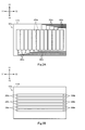
Fig. 1A is a schematic bottom view of a touch panel in accordance with an embodiment of the invention. -
Fig. 1B is a sectional view of the touch panel taken along 1B-1B inFig. 1A . -
Fig. 2A is a schematic bottom view of a first translucent base of the touch panel, on which first electrodes and first leads are formed. -
Fig. 2B is a schematic bottom view of a second translucent base of the touch panel, on which second electrodes and second leads are formed. -
Fig. 3A illustrates steps of forming the second translucent base, the second electrodes, the second leads, a second protective layer, and a second low reflective member of the touch panel. -
Fig. 3B illustrates steps of forming the first translucent base, the first electrodes, the first leads, a first protective layer, and a first low reflective member of the touch panel. -
Fig. 3C illustrates steps of laminating first and second laminates of the touch panel to each other, and a process of connecting an FPC. -
Fig. 4 is a sectional view of a first variant of the touch panel. -
Fig. 5 is a sectional view of a second variant of the touch panel. - In the brief description of drawings above and in the description which follows, relative spatial terms such as "upper", "lower", "top", "bottom", "right", "front", "rear", "under", etc., are used for the convenience of the skilled reader and refer to the orientation of the touch panel and its constituent parts as depicted in the drawings. No limitation is intended by use of these terms, either in use of the invention, during its manufacture, shipment, custody, or sale, or during assembly of its constituent parts or when incorporated into or combined with other apparatus.
- A touch panel in accordance with an embodiment of the invention will be described with reference to
Fig. 1A to Fig. 3C . The touch panel T shown inFig. 1A and Fig. 1B is a projected capacitive touch panel. The touch panel T includes first and second laminated bodies, a flexible printed circuit (FPC) 600 (external connection part), and a transparentadhesive layer 700. Each constituent of the touch panel T will be described below in detail. InFig. 1A to Fig. 2B , X1 represents one widthwise side of the touch panel T, and X2 represents the other widthwise side of the touch panel T. Y1 represents one lengthwise side of the touch panel T, and Y2 represents the other lengthwise side of the touch panel T. Z1 represents one thicknesswise end of the touch panel T, and Z2 represents the other thicknesswise end of the touch panel T. The Y1-Y2 direction is orthogonal to the X1-X2 direction. The Z1-Z2 direction is orthogonal to Y1-Y2 and X1-X2 directions. - The first laminated body includes a first
translucent base 100a, a plurality offirst electrodes 200a, a plurality offirst leads 300a, a firstprotective layer 400a, and a first lowreflective member 500a. The second laminated body includes a secondtranslucent base 100b, a plurality ofsecond electrodes 200b, a plurality ofsecond leads 300b, a secondprotective layer 400b, and a second lowreflective member 500b. - The second
translucent base 100b as shown inFig. 1A, Fig. 1B , andFig. 2B is a transparent glass sheet. The secondtranslucent base 100b has a thickness in the range of 0.05 mm to 2.0 mm. It is more preferable that the secondtranslucent base 100b have a thickness of 1.1 mm because of the optimum balance between low material cost of the secondtranslucent base 100b and high sensitivity of thesecond electrodes 200b on the secondtranslucent base 100b. The secondtranslucent base 100b has afirst face 110b and asecond face 120b, which is on the back side from thefirst face 110b. Thesecond face 120b is located on the sensing side (front side (Z1 side)) of the touch panel T, and thefirst face 110b is located on a non-sensing side (back side (Z2 side)) of the touch panel T. In other words, thesecond face 120b is located closer to atouch sensing face 520b than thefirst face 110b in the Z1-Z2 direction. An ornamental layer may be provided on thesecond face 120b so as to cover the first leads 300a and/orsecond leads 300b. - The second low
reflective member 500b as shown inFig. 1B is a polarizing plate or film that is subjected to anti-glare treatment and/or low-reflection treatment. The second lowreflective member 500b is laminated on thesecond face 120b of the secondtranslucent base 100b. The second lowreflective member 500b is the uppermost layer of the touch panel T. The second lowreflective member 500b has a fixingface 510b and thetouch sensing face 520b on the back side from the fixingface 510b. The fixingface 510b is fixed on thesecond face 120b of the secondtranslucent base 100b. Substantially no air layer is present between the fixingface 510b of the second lowreflective member 500b and thesecond face 120b of the secondtranslucent base 100b. Thetouch sensing face 520b is the outer face (top face) of the touch panel T, onto which a detection object such as a finger or a touch pen is touchable. When the secondtranslucent base 100b is broken, the second lowreflective member 500b can prevent scattering of the secondtranslucent base 100b. - The
second electrodes 200b as shown inFig. 1A, Fig. 1B , andFig. 2B are transparent conductive film strips, conductive wires, or other conductors that extend in the Y1-Y2 direction. Thesecond electrodes 200b are arranged at intervals along the X1-X2 direction on thefirst face 110b of the secondtranslucent base 100b. The transparent conductive film strips may be formed of indium tin oxide (ITO), indium-doped zinc oxide (IZO), aluminum-doped zinc oxide (AZO), or conductive polymer such as PEDOT and PSS. The conductive wires may be silver (Ag) nanowires or metal wires each having a width of 15 µm or smaller. The conductors may be of photosensitive silver. The conductors may be electrically conductive lines of silver, copper, or other metal, each having a width of 15 µm or smaller, and may be fabricated by graph offset or other method. - The second leads 300b as shown in
Fig. 1A, Fig. 1B , andFig. 2B are transparent conductive film strips, strips of metal (e.g. silver (Ag), molybdenum (Mo), aluminum (Al), or copper (Cu)), strips of metal alloy (e.g. alloy of silver (Ag), palladium (Pd), and copper (Cu)), or metal wires. The transparent conductive film strips may be made of the same material as that of the transparent conductive film strips of thesecond electrode 200b. The second leads 300b are arranged at intervals on thefirst face 110b of the secondtranslucent base 100b. The second leads 300b each have first and second ends. The first ends of the second leads 300b are connected to respective ends of thesecond electrodes 200b. - In the case where the
second electrodes 200b are transparent conductive film strips, a transparent second index matching layer IMb (second refractive-index adjusting layer) may optionally be provided on thefirst face 110b of the secondtranslucent base 100b. In this case, thesecond electrodes 200a and the second leads 300b are provided on the second index matching layer IMb on thefirst face 110b. The second index matching layer IMb is interposed between the secondtranslucent base 100b and thesecond electrodes 200b. The transparent conductive film strips serving as thesecond electrodes 200b has a refractive index in the range of about 1.9 to about 2.0. The material (glass) used for the secondtranslucent base 100b generally has a refractive index in the range of 1.4 to 1.6. The second index matching layer IMb has a refractive index larger than that of the secondtranslucent base 100b and smaller than that of the transparent conductive film strips used for thesecond electrodes 200b. Therefore, the second index matching layer IMb functions to reduce (adjust) the difference in refractive index between the secondtranslucent base 100b and thesecond electrodes 200b. It should be noted that the second index matching layer IMb is illustrated inFig. 1B but not inFig. 2B to Fig. 3C . - The second
protective layer 400b as shown inFig. 1B is made of transparent acrylic resin. The secondprotective layer 400b is laminated on thefirst face 110b of the secondtranslucent base 100b so as to cover thesecond electrodes 200b and the second leads 300b excluding their second ends. Substantially no air layer is present between the secondprotective layer 400b and thefirst face 110b of the secondtranslucent base 100b. - The first
translucent base 100a as shown inFig. 1A to Fig. 2A is a transparent glass sheet. The firsttranslucent base 100a has a thickness in the range of 0.05 mm to 2.0 mm. It is more preferable that the firsttranslucent base 100a have a thickness 0.55 mm because of the optimum balance between low material cost of the firsttranslucent base 100a and high sensitivity of thefirst electrodes 200a on the firsttranslucent base 100a. The firsttranslucent base 100a has afirst face 110a and asecond face 120a, which is on the back side from thefirst face 110a. Thesecond face 120a is fixed to the secondprotective layer 400b with the transparentadhesive layer 700. Thesecond face 120a faces thefirst face 110b of the secondtranslucent base 100b. Thesecond face 120a is located on the sensing side (front side (Z1 side)) of the touch panel T, and thefirst face 110a is located on the non-sensing side (back side (Z2 side)) of the touch panel T. In other words, thefirst face 110a is located farther from thetouch sensing face 520b than thesecond face 120a in the Z1-Z2 direction. - The
first electrodes 200a as shown inFig. 1A to Fig. 2A are transparent conductive film strips, conductive wires, or other conductors that extend in the X1-X2 direction. Thefirst electrodes 200a are arranged at intervals along the Y1-Y2 direction on thefirst face 110a of the firsttranslucent base 100a. Thefirst electrodes 200a intersect with thesecond electrodes 200b at substantially right angles in planar position. The transparent conductive film strips are formed of indium tin oxide (ITO), indium-doped zinc oxide (IZO), aluminum-doped zinc oxide (AZO), or conductive polymer such as PEDOT and PSS. The conductive wires may be silver (Ag) nanowires or metal wires each having a width of 15 µm or smaller. The conductors may be of photosensitive silver. The conductors may be electrically conductive lines of silver, copper, or other metal, each having a width of 15 µm or smaller, and may be fabricated by graph offset or other method. - It is apparent that the conductive wires or other conductors of the first and
second electrodes second electrodes second electrodes second electrodes - The first leads 300a as shown in
Fig. 1B to Fig. 2A are transparent conductive film strips, or strips of metal (e.g. silver (Ag), molybdenum (Mo), aluminum (Al), or copper (Cu)), strips of metal alloy (e.g. alloy of silver (Ag), palladium (Pd), and copper (Cu)), or metal wires. The transparent conductive film strips may be made of the same material as that of the transparent conductive film strips of thefirst electrodes 200a. Thefirst leads 300a are arranged at intervals on thefirst face 110a of the firsttranslucent base 100a. The first leads 300a have first and second ends. Thefirst leads 300a are routed such that their first ends are connected to respective X1-direction ends or respective X2-direction ends of thefirst electrodes 200a, and that their second ends are located at either right side corner, as shown inFig. 2A , of thefirst face 110a of the firsttranslucent base 100a. - In the case where the
first electrodes 200a are transparent conductive film strips, a transparent first index matching layer IMa (first refractive-index adjusting layer) may optionally be provided, as shown, on thefirst face 110a of the firsttranslucent base 100a. In this case, thefirst electrodes 200a and thefirst leads 300a are provided on the first index matching layer IMa on thefirst face 110a. The first index matching layer IMa is interposed between the firsttranslucent base 100a and thefirst electrodes 200a. The transparent conductive film strips serving as thefirst electrodes 200a has a refractive index in the range of about 1.9 to about 2.0. The material (glass) used for the firsttranslucent base 100a generally has a refractive index in the range of 1.4 to 1.6. The first index matching layer IMa has a refractive index larger than that of the firsttranslucent base 100a and smaller than that of the transparent conductive film strips used for thefirst electrodes 200a. Therefore, the first index matching layer IMa functions to reduce (adjust) the difference in refractive index between the firsttranslucent base 100a and thefirst electrodes 200a. It should be noted that the first index matching layer IMa is illustrated inFig. 1B but not inFig. 2A andFig. 3A toFig. 3C . - The first
protective layer 400a as shown inFig. 1B is made of transparent acrylic resin. The firstprotective layer 400a is laminated on thefirst face 110a of the firsttranslucent base 100a so as to cover thefirst electrodes 200a and thefirst leads 300a excluding their second ends. Substantially no air layer is present between the firstprotective layer 400a and thefirst face 110a of the firsttranslucent base 100a. - The first low
reflective member 500a as shown inFig. 1A to Fig. 1B is a low reflective (LR) film. The first lowreflective member 500a is provided on the firstprotective layer 400a so as to cover thefirst electrodes 200a and thefirst leads 300a excluding their second ends. The first lowreflective member 500a is the lowermost layer of the touch panel T. The firstprotective layer 400a and the first lowreflective member 500a protect thefirst electrodes 200a and thefirst leads 300a. Substantially no air layer is present between the first lowreflective member 500a and the firstprotective layer 400a. - As shown in
Fig. 1A and Fig. 1B , theFPC 600 includes a pair of first connectingportions 610 and a second connectingportion 620. The first connectingportions 610 extend from the opposite ends of the second connectingportion 620. The first connectingportions 610 are fixed to the above-described corners of thefirst face 110a of the firsttranslucent base 100a and connected to the second ends of thefirst leads 300a. The second connectingportion 620 is fixed to thefirst face 110b of the secondtranslucent base 100b and connected to the second leads 300b. TheFPC 600 is used to connect the touch panel T to electronic equipment such as a mobile terminal or a display. - The touch panel T configured as described above may be fabricated in the steps as described below and as illustrated in
Fig. 3A to Fig. 3C . By way of example, it is assumed that the first andsecond electrodes first leads 300a are formed of silver. - The second laminated body (the second low
reflective member 500b, the secondtranslucent base 100b, thesecond electrodes 200b, the second leads 300b, and the secondprotective layer 400b) of the touch panel T may be formed in the following steps. First, the secondtranslucent base 100b and an index matching film are prepared. The index matching film (second index matching layer IMb, not shown) is affixed to thefirst face 110b of the secondtranslucent base 100b. An ITO film is formed on the second index matching layer IMb of thefirst face 110b. The ITO film is subjected to patterning by etching or other well-known method. As a result, as shown inFig. 3A , on the second index matching layer IMb on thefirst face 110b of the secondtranslucent base 100b, there are formed thesecond electrodes 200b at intervals and the second leads 300b contiguous with thesecond electrodes 200b (arranged as shown inFig. 2B ). - After that, transparent acrylic resin is applied onto the second index matching layer IMb on the
first face 110b of the secondtranslucent base 100b. Care should be taken here to see that there is no air layer formed between the acrylic resin and the second index matching layer IMb. The applied acrylic resin forms the secondprotective layer 400b. The secondprotective layer 400b is thus fixed to the second index matching layer IMb on thefirst face 110b so as to cover thesecond electrodes 200b and the second leads 300b excluding their second ends on the second index matching layer IMb. After that, the fixingface 510b of the second lowreflective member 500b is fixed to thesecond face 120b of the secondtranslucent base 100b, with care not to form an air layer between thesecond face 120b of the secondtranslucent base 100b and the fixingface 510b of the second lowreflective member 500b. If providing an ornamental layer on thesecond face 120b of the secondtranslucent base 100b, the ornamental layer may be formed by performing screen printing or gravure printing on thesecond face 120b or by affixing a decorative film on thesecond face 120b, before affixing the second lowreflective member 500b onto thesecond face 120b. - On the other hand, the first laminated body (the first
translucent base 100a, thefirst electrodes 200a, thefirst leads 300a, the firstprotective layer 400a, and the first lowreflective member 500a) of the touch panel T may be formed in the following steps. First, the firsttranslucent base 100a and an index matching film are prepared. The index matching film (first index matching layer IMa, not shown) is affixed to thefirst face 110a of the firsttranslucent base 100a. An ITO film is formed on the first index matching layer IMa of thefirst face 110a. The ITO film is subjected to patterning by etching or other well-known method. As a result, as shown inFig. 3B , thefirst electrodes 200a are formed at intervals on the first index matching layer IMa on thefirst face 110a of the firsttranslucent base 100a. After that, silver wire printing is made on the first index matching layer IMa on thefirst face 110a of the firsttranslucent base 100a to form thefirst leads 300a. The printing is made such that the first ends of thefirst leads 300a overlap the associated X1- and X2-direction ends of thefirst electrodes 200a. Thefirst leads 300a are thus connected to thefirst electrodes 200a. - After that, transparent acrylic resin is applied to the first index matching layer IMa on the
first face 110a of the firsttranslucent base 100a. Care should be taken here to see that there is no air layer formed between the acrylic resin and the first index matching layer IMa. The applied acrylic resin forms the firstprotective layer 400a. The firstprotective layer 400a is thus fixed to the first index matching layer IMa on thefirst face 110a so as to cover thefirst electrodes 200a and thefirst leads 300a excluding their second ends on the first index matching layer IMa. After that, the firstprotective layer 400a is affixed to the first lowreflective member 500a, with care not to form an air layer between the firstprotective layer 400a and the first lowreflective member 500a. As a result, the first lowreflective member 500a covers and protects thefirst electrodes 200a on the first index matching layer IMa on thefirst face 110a. - The next step is to bond the second laminated body of the touch panel T to the first laminated body of the touch panel T. More specifically, an adhesive (to form transparent adhesive layer 700) is applied to the second
protective layer 400b and/or thesecond face 120b of the firsttranslucent base 100a. The secondprotective layer 400b is then affixed to thesecond face 120b of the firsttranslucent base 100a with the transparentadhesive layer 700. The second laminated body of the touch panel T and the first laminated body of the touch panel T are thus bonded together, with thesecond electrodes 200b intersecting with thefirst electrodes 200a at substantially right angles in planar position. - The
FPC 600 is also prepared. The first connectingportions 610 of theFPC 600 are crimped with an anisotropic conductive film onto thefirst face 110a of the firsttranslucent base 100a. The first connectingportions 610 are thus connected to thefirst leads 300a. Similarly, the second connectingportion 620 of theFPC 600 is crimped with an anisotropic conductive film onto thefirst face 110b of the secondtranslucent base 100b. The second connectingportion 620 is thus connected to the second leads 300b. - The touch panel T has at least the following technical features. First, the touch panel T is configured to prevent damage to the first and
second electrodes first electrodes 200a are formed on thefirst face 110a, the firstprotective layer 400a is formed on thefirst face 110a so as to cover thefirst electrodes 200a, and the first lowreflective member 500a is fixed to the firstprotective layer 400a so as to cover the first electrodes 200a.Thefirst electrodes 200a are thus covered with the firstprotective layer 400a and the first lowreflective member 500a and therefore protected from damage during and after the manufacture of the touch panel T. Similarly, in manufacturing the second laminated body, thesecond electrodes 200b are formed on thefirst face 110b, and the secondprotective layer 400b is formed on thefirst face 110b so as to cover thesecond electrodes 200b. Thesecond electrodes 200b are thus covered with the secondprotective layer 400b and therefore protected from damage during and after the manufacture of the touch panel T. - Second, the touch panel T has an improved visibility for the following reasons. Generally speaking, if the first electrodes are disposed on a different layer that substantially differs in refractive index from the first electrodes (if the first electrodes are exposed, the different layer is an air layer (refractive index = 1)), light reflects at the boundary of the first electrodes and the different layer. In contrast, the
first electrodes 200a of the touch panel T are covered with the firstprotective layer 400a and the first lowreflective member 500a. The firstprotective layer 400a and the first lowreflective member 500a have refractive indexes close to that of thefirst electrodes 200a, reducing light reflection from the boundary between thefirst electrodes 200a and the firstprotective layer 400a and the first lowreflective member 500a. The reduction in light reflection is advantageously achieved especially by the first lowreflective member 500a covering thefirst electrodes 200a. Further, in the case where the first index matching layer IMa is interposed between the firsttranslucent base 100a and thefirst electrodes 200a, the first index matching layer IMa serves to decrease the difference in refractive index between the firsttranslucent base 100a and thefirst electrodes 200a. This can reduce light reflection at the boundary between the firsttranslucent base 100a and thefirst electrodes 200a. In the case where the second index matching layer IMb is interposed between the secondtranslucent base 100b and thesecond electrodes 200b, the second index matching layer IMb serves to decrease the difference in refractive index between the secondtranslucent base 100b and thesecond electrodes 200b. This can reduce light reflection form the boundary between the secondtranslucent base 100b and thesecond electrodes 200b. The second lowreflective member 500b also suppresses light reflection. - Third, the first low
reflective member 500a serves to suppress light reflection and protects thefirst electrodes 200a, while the second lowreflective member 500b serves to suppress light reflection and prevent scattering of the secondtranslucent base 100b, if broken. The first and second lowreflective members - Fourth, the touch panel T can provide higher sensitivity at lower cost for the following reasons. The first and second
translucent bases translucent bases second electrodes - The touch panel T is not limited to the embodiment described above but may be modified in any manner within the scope of the claims. Specific modifications will be described below in detail.
- The
second electrodes 200b of the embodiment are arranged at intervals on thefirst face 110b of the secondtranslucent base 100b so as to intersect with thefirst electrodes 200a at right angles in planar position. However, the second electrodes of the invention may be arranged in any manner as long as they intersect with the first electrodes in planar position. For example, as in a modified touch panel T' shown inFig. 4 , thesecond electrodes 200b' may be arranged at intervals along the X1-X2 direction on thesecond face 120a of the firsttranslucent base 100a and extend in the Y1-Y2 direction. Thesecond electrodes 200b' may intersect with thefirst electrodes 200a at substantially right angles. Second leads 300b' may be provided on thesecond face 120a of the firsttranslucent base 100a, as in the touch panel T. A secondprotective layer 400b' may be provided on thesecond face 120a of the firsttranslucent base 100a so as to cover thesecond electrodes 200b' and the second leads 300b' excluding their second ends. A second lowreflective member 500b' may be laminated on the secondprotective layer 400b'. The first index matching layer IMa may be provided on thefirst face 110a of the firsttranslucent base 100a as in the touch panel T, while a second index matching layer IMb' may be provided on thesecond face 120a of the firsttranslucent base 100a. Thefirst electrodes 200a may be provided on the first index matching layer IMa as in the touch panel T, while thesecond electrodes 200b' may be provided on the second index matching layer IMb'. - Alternatively, as in another modified touch panel T" in which an insulating
film 800 is provided on thefirst face 110a of the firsttranslucent base 100a so as to cover thefirst electrodes 200a, thesecond electrodes 200b" may be arranged at intervals along the X1-X2 direction on the insulatingfilm 800 and extend in the Y1-Y2 direction. Thesecond electrodes 200b" may intersect with thefirst electrodes 200a at substantially right angles. Second leads 300b" may be arranged at intervals on thefirst face 110a of the firsttranslucent base 100a. The second leads 300b" may each have first and second ends and be routed such that the first ends are connected to respective Y2-direction ends of thesecond electrodes 200b", and that the second ends are located at the right end (as shown inFig. 2A ) of thefirst face 110a of the firsttranslucent base 100a. Although not shown inFig. 5 , thefirst leads 300a may be provided on thefirst face 110a of the firsttranslucent base 100a as in the embodiment. A firstprotective layer 400a' may be provided on the insulatingfilm 800 and on thefirst face 110a of the firsttranslucent base 100a so as to cover the first andsecond electrodes second leads reflective member 500a' may be provided on the firstprotective layer 400a' so as to cover the first andsecond electrodes second leads reflective member 500b" may be laminated on thesecond face 120a of the firsttranslucent base 100a. An FPC 600' may be fixed to thefirst face 110a of the firsttranslucent base 100a and connected to the second ends of the first andsecond leads first face 110a of the firsttranslucent base 100a. If provided, thefirst electrodes 200a may be provided on the first index matching layer IMa on thefirst face 110a. - In the embodiment and the modifications described above, the first
translucent base 100a is a transparent glass sheet having the first andsecond faces - The first electrodes of the invention may be modified in any manner as long as they are arranged at intervals on the first face of the first translucent base of any aspect described above. The first electrodes of the invention may be provided directly on the first face of the first translucent base, or on the index matching layer on the first face of the first translucent base.
- The first low reflective member of the invention may be any member adapted to reduce light reflection and cover the first electrodes. For example, the touch panels T and/or T' may be modified such that the first low
reflective member 500a is provided on thefirst face 110a of the firsttranslucent base 100a so as to cover thefirst electrodes 200a. In this case, the firstprotective layer 400a can be omitted. The touch panel T" may be modified such that the first lowreflective member 500a' is provided on the insulatingfilm 800 so as to cover the first andsecond electrodes protective layer 400a' can be omitted. The first low reflective member of the invention may not be the lowermost layer of the touch panel of the invention, which may include another layer, such as a protective layer, under the first low reflective member. The first low reflective member of any aspect described above may be a polarizing plate or film subjected to anti-glare treatment and/or low-reflection treatment. - The second translucent base can be omitted in the invention, as in the touch panel T' and T". Alternatively, the second translucent base of the invention may be any translucent member having a first face and a second face on the back side from the first face, wherein the first face is opposed to the second face of the first translucent base. For example, the second translucent base may be a film of translucent resin such as PET. The second translucent base may alternatively be a translucent rigid sheet glass or translucent rigid resin film, or a translucent flexible sheet glass or translucent flexible resin film. The second translucent base, if formed of rigid or flexible glass, may have a thickness as described for the above embodiment.
- The invention can be realized without the second low reflective member. The invention can also be realized with the second low reflective member replaced with a protective layer on the second face of the second translucent base or the second face of the first translucent base. The second low reflective member may not be the uppermost layer of the touch panel of the invention, which may include another layer such as a protective layer or a decorative panel on top of the second low reflective member. The touch sensing face of the invention may be any top face of the touch panel or an outer face of the touch sensing part of electronic equipment to install the touch panel. The second low reflective member of the invention may be of any material adapted to reduce light reflection. For example, the second low reflective member may be an LR film.
- The invention can be realized without the first index matching layer and/or the second index matching layer. The first index matching layer may be provided on the first face of the first translucent base even if the first electrodes are not the transparent conductive film strips but formed of other material. The first index matching layer may be of any material having a refractive index larger than that of the first translucent base and smaller than that of the first electrodes. In the case where the first index matching layer is provided on the first face of the first translucent base, the first leads may also be provided on this first face. If the second electrodes are not the transparent conductive film strips but formed of other material, the second index matching layer may be provided on the first face of the second translucent base or on the second face of the first translucent base. The second index matching layer may be of any material with a refractive index larger than that of the first translucent base or than that of the second translucent base, and smaller than that of the second electrodes. In the case where the second index matching layer is provided on the first face of the second translucent base or on the second face of the first translucent base, the second leads may also be provided on the first face of the second translucent base or on the second face of the first translucent base.
- The invention can be realized without the first protective layer and/or the second protective layer. When the first protective layer is omitted, the first low reflective member may be provided on the first face of the first translucent base of any aspect described above so as to cover at least the first electrodes. When the second protective layer is omitted, the second face of the first translucent base may be fixed to the first face of the second translucent base or to the second low reflective member.
- The first protective layer of the invention may be any translucent member adapted to cover the first electrodes and/or the first leads. For example, the touch panels T and T' may be modified such that the first
protective layer 400a covers thefirst electrodes 200a partly or entirely or covers thefirst leads 300a excluding their second ends. In this case, the first lowreflective member 500a may be provided on the firstprotective layer 400a and on thefirst face 110a of the firsttranslucent base 100a so as to cover thefirst electrodes 200a. The touch panel T" may be modified such that the firstprotective layer 400a' covers the first andsecond electrodes second leads reflective member 500a' may be provided on the firstprotective layer 400a' and on the insulatingfilm 800 so as to cover the first andsecond electrodes - The second protective layer of the invention may be any translucent member adapted to cover the second electrodes and/or the second leads. For example, the touch panel T may be modified such that the second
protective layer 400b covers thesecond electrodes 200b partly or entirely or covers the second leads 300b excluding their second ends. In this case, thesecond face 120a of the firsttranslucent base 100a may be fixed on the secondprotective layer 400b and on thefirst face 110b of the secondtranslucent base 100b. The touch panel T' may be modified such that the secondprotective layer 400b' covers thesecond electrodes 200b' partly or entirely or covers the second leads 300b' excluding their second ends. In this case, the second lowreflective member 500b' may be fixed on the secondprotective layer 400b' and on thesecond face 120a of the firsttranslucent base 100a. - The external connection part of the invention may be an FPC as in the embodiment and the modifications described above. The external connection part may be any member adapted to connect the first and second electrodes to the outside. For example, the external connection part may be pins or a connector connectable with the first and second electrodes. Alternatively, the external connection part may be portions of the first and second leads.
- The touch panel of the invention may be manufactured by any method including preparing a first translucent base, forming a plurality of first electrodes on a first face of the first translucent base, fixing a first low reflective member onto the first face of the first translucent base so as to cover the first electrodes, preparing a second translucent base, forming a plurality of second electrodes on a first face of the second translucent base, forming a protective layer (second protective layer) on the first face of the second translucent base so as to cover the second electrodes, and a second face on the back side from the first face of the first translucent base to the protective layer. Before forming the first electrodes on the first face of the first translucent base, the first index matching layer may be provided on the first face of the first translucent base and the first electrodes may then be provided on the first index matching layer. Before forming the second electrodes on the first face of the second translucent base, the second index matching layer may be provided on the first face of the second translucent base and the second electrodes may then be formed on the second index matching layer. Before fixing the first low reflective member, the first protective layer may be provided on the first face of the first translucent base so as to cover the first electrodes, and the first low reflective member may be fixed onto the first protective layer. The second low reflective member may be fixed to the second face on the back side of the second translucent base from the first face.
- It should be appreciated that the embodiment and modifications are described above by way of example only. The materials, shapes, dimensions, numbers, arrangements, and other configurations of the constituents of the touch panel may be modified in any manner if they can perform similar functions. The configurations of the embodiment and the modifications described above may be combined in any possible manner.
-
- 100a: first translucent base
- 110a: first face
- 120a: second face
- 100b: second translucent base
- 110b: first face
- 120b: second face
- 200a: first electrodes
- 200b: second electrodes
- 300a: first leads
- 300b: second leads
- 400a: first protective layer
- 400b: second protective layer
- 500a: first low reflective member
- 500b: second low reflective member
- 600: FPC (external connection part)
- 700: adhesive layer
- IMa: first index matching layer
- IMb: second index matching layer
Claims (12)
- A touch panel (T, T', T") comprising:a first translucent base (100a), the first translucent base including:a first face (110a) on a non-sensing side of the touch panel, anda second face (120a) on a sensing side of the touch panel;a plurality of first electrodes (200a) arranged at intervals on the first face of the first translucent base; anda first low reflective member (500a, 500a') configured to cover the first electrodes.
- The touch panel (T) according to claim 1, further comprising:a second translucent base (100b), the second translucent base including:a first face (110b) disposed on the second face (120a) of the first translucent base (100a), anda second face (120b) on the back side from the first face;a plurality of second electrodes (200b) arranged at intervals on the first face of the second translucent base, the second electrodes intersecting with the first electrodes (200a) in planar position; anda second low reflective member (500b) on the second face of the second translucent base.
- The touch panel (T) according to claim 2, further comprising:a plurality of first leads (300a) arranged at intervals on the first face (110a) of the first translucent base (100a), the first leads being connected to the first electrodes (200a);a first protective layer (400a) to cover the first electrodes, the first leads, or both;a plurality of second leads (300b) arranged at intervals on the first face (110b) of the second translucent base (100b), the second leads being connected to the second electrodes (200b); anda second protective layer (400b) to cover the second electrodes, the second leads, or both, whereinthe second face (120a) of the first translucent base is fixed to at least one of the first face of the second translucent base and the second protective layer, andthe first low reflective member (500a) is provided on at least one of the first face of the first translucent base and the first protective layer so as to cover the first electrodes.
- The touch panel (T) according to claim 3, further comprising:a first index matching layer (IMa) on the first face (110a) of the first translucent base (100a), the first index matching layer existing at least between the first translucent base and the first electrodes (200a); anda second index matching layer (1Mb) on the first face (110b) of the second translucent base (100b), the second index matching layer existing at least between the second translucent base and the second electrodes (200b), whereinthe first protective layer (400a) is provided on at least one of the first face of the first translucent base and the first index matching layer so as to cover the first electrodes, the first leads (300a), or both, andthe second protective layer (400b) is provided on at least one of the first face of the second translucent base and the second index matching layer so as to cover the second electrodes, the second leads (300b), or both.
- The touch panel (T') according to claim 1, further comprising:a plurality of second electrodes (200b') arranged at intervals on the second face (120a) of the first translucent base (100a), the second electrodes intersecting with the first electrodes (200a) in planar position; anda second low reflective member (500b') to cover the second electrodes.
- The touch panel (T') according to claim 5, further comprising:a plurality of first leads (300a) arranged at intervals on the first face (110a) of the first translucent base (100a), the first leads being connected to the first electrodes (200a);a first protective layer (400a) to cover: the first electrodes; the first leads; or both;a plurality of second leads (300b') arranged at intervals on the second face (120a) of the first translucent base, the second leads being connected to the second electrodes (200b');a second protective layer (400b') to cover the second electrodes, the second leads, or both, whereinthe first low reflective member (500a) is provided on at least one of the first face of the first translucent base and the first protective layer to cover the first electrodes, andthe second low reflective member (500b') is provided on at least one of the second face of the first translucent base and the second protective layer so as to cover the second electrodes.
- The touch panel (T') according to claim 6, further comprising:a first index matching layer (IMa) on the first face (110a) of the first translucent base (100a), the first index matching layer existing at least between the first translucent base and the first electrodes (200a); anda second index matching layer (IMb') on the second face (120a) of the first translucent base, the second index matching layer existing at least between the first translucent base and the second electrodes (200b'), whereinthe first protective layer (400a) is provided on at least one of the first face of the first translucent base and the first index matching layer so as to cover the first electrodes, the first leads (300a), or both, andthe second protective layer (400b') provided on at least one of the second face of the first translucent base and the second index matching layer so as to cover the second electrodes, the second leads (300b'), or both.
- The touch panel (T") according to claim 1, further comprising:an insulating film (800) on the first face (110a) of the first translucent base (100a) so as to cover the first electrodes (200a);a plurality of second electrodes (200b") arranged at intervals on the insulating film, the second electrodes intersecting with the first electrodes in planar position; anda second low reflective member (500b") on the second face (120a) of the first translucent base, whereinthe first low reflective member (500a') covers the first and second electrodes.
- The touch panel (T") according to claim 8, further comprising:a plurality of first leads (300a) arranged at intervals on the first face (110a) of the first translucent base (100a), the first leads being connected to the first electrodes (200a);a plurality of second leads (300b") arranged at intervals on the first face of the first translucent base, the second leads being connected to the second electrodes (200b"); anda first protective layer (400a') to cover the first and second electrodes or the first and second leads, whereinthe first low reflective member (500a') is provided on at least one of the insulating film (800) and the first protective layer so as to cover the first and second electrodes.
- The touch panel (T") according to claim 9, further comprising a first index matching layer (IMa) on the first face (110a) of the first translucent base (100a), the first index matching layer existing at least between the first translucent base and the first electrodes (200a).
- The touch panel (T, T', T") according to any one of claims 1 to 8, wherein
the first translucent base (100a) is made of glass and has a thickness in the range of 0.05 mm to 2.0 mm. - The touch panel (T, T', T") according to any one of claims 2 to 4, wherein
the second translucent base (100b) is made of glass and has a thickness in the range of 0.05 mm to 2.0 mm.
Applications Claiming Priority (2)
| Application Number | Priority Date | Filing Date | Title |
|---|---|---|---|
| JP2013036812 | 2013-02-27 | ||
| JP2013255699A JP2014194749A (en) | 2013-02-27 | 2013-12-11 | Touch panel |
Publications (1)
| Publication Number | Publication Date |
|---|---|
| EP2772839A2 true EP2772839A2 (en) | 2014-09-03 |
Family
ID=50272538
Family Applications (1)
| Application Number | Title | Priority Date | Filing Date |
|---|---|---|---|
| EP14250024.8A Withdrawn EP2772839A2 (en) | 2013-02-27 | 2014-02-12 | Touch panel |
Country Status (6)
| Country | Link |
|---|---|
| US (1) | US20140240619A1 (en) |
| EP (1) | EP2772839A2 (en) |
| JP (1) | JP2014194749A (en) |
| KR (1) | KR20140107113A (en) |
| CN (1) | CN104007872A (en) |
| TW (1) | TW201441892A (en) |
Families Citing this family (9)
| Publication number | Priority date | Publication date | Assignee | Title |
|---|---|---|---|---|
| CN103490648B (en) * | 2013-10-10 | 2015-12-09 | 成都芯源系统有限公司 | Isolated switch converter and control method thereof |
| US9541965B1 (en) * | 2014-03-10 | 2017-01-10 | Amazon Technologies, Inc. | Cover assembly for a display stack |
| US10318026B2 (en) | 2014-12-09 | 2019-06-11 | Lg Innotek Co., Ltd. | Touch window |
| CN104699309B (en) * | 2015-03-31 | 2017-06-13 | 合肥京东方光电科技有限公司 | A kind of touch-screen, its preparation method and display device |
| JP6052330B2 (en) * | 2015-04-24 | 2016-12-27 | Tdk株式会社 | Transparent conductor, manufacturing method thereof, and touch panel |
| CN105260050A (en) * | 2015-09-10 | 2016-01-20 | 昆山龙腾光电有限公司 | Embedded touch control display device |
| CN105138191B (en) | 2015-10-15 | 2019-02-26 | 京东方科技集团股份有限公司 | A touch display device and its manufacturing method |
| JP6814106B2 (en) * | 2017-08-01 | 2021-01-13 | ホシデン株式会社 | Touch input device |
| US10923002B1 (en) * | 2019-08-29 | 2021-02-16 | Wuhan China Star Optoelectronics Semiconductor Display Technology Co., Ltd. | Flexible display device |
Citations (1)
| Publication number | Priority date | Publication date | Assignee | Title |
|---|---|---|---|---|
| JP2009259063A (en) | 2008-04-18 | 2009-11-05 | Gunze Ltd | Touch panel and its production method |
Family Cites Families (12)
| Publication number | Priority date | Publication date | Assignee | Title |
|---|---|---|---|---|
| JP3779515B2 (en) * | 1999-11-10 | 2006-05-31 | グンゼ株式会社 | Touch panel |
| JP4632589B2 (en) * | 2001-08-06 | 2011-02-16 | 大日本印刷株式会社 | Transparent touch panel with antireflection function and display device using the same |
| JP5413937B2 (en) * | 2006-09-28 | 2014-02-12 | 株式会社ジャパンディスプレイ | Electro-optical device and electronic apparatus |
| US20090096763A1 (en) * | 2007-10-16 | 2009-04-16 | Epson Imaging Devices Corporation | Touch panel, display device with input function, and electronic apparatus |
| CN101498972B (en) * | 2008-02-01 | 2012-07-18 | 台达电子工业股份有限公司 | touch panel |
| JP4958020B2 (en) * | 2009-03-31 | 2012-06-20 | 大日本印刷株式会社 | Touch panel sensor, laminate for manufacturing touch panel sensor, and method for manufacturing touch panel sensor |
| US20110012845A1 (en) * | 2009-07-20 | 2011-01-20 | Rothkopf Fletcher R | Touch sensor structures for displays |
| US20110012841A1 (en) * | 2009-07-20 | 2011-01-20 | Teh-Zheng Lin | Transparent touch panel capable of being arranged before display of electronic device |
| KR101122949B1 (en) * | 2010-04-28 | 2012-06-12 | 삼성모바일디스플레이주식회사 | Touch screen panel and fabricating method for the same |
| JP2012138019A (en) * | 2010-12-27 | 2012-07-19 | Dainippon Printing Co Ltd | Display device with touch panel |
| KR101294569B1 (en) * | 2011-06-29 | 2013-08-07 | 엘지이노텍 주식회사 | Touch panel and method for manufacturing the same |
| US9079384B2 (en) * | 2011-11-11 | 2015-07-14 | Apple Inc. | Touch sensor panel having an index matching passivation layer |
-
2013
- 2013-12-11 JP JP2013255699A patent/JP2014194749A/en active Pending
-
2014
- 2014-01-09 TW TW103100816A patent/TW201441892A/en unknown
- 2014-01-15 KR KR1020140004915A patent/KR20140107113A/en not_active Withdrawn
- 2014-02-12 EP EP14250024.8A patent/EP2772839A2/en not_active Withdrawn
- 2014-02-24 US US14/187,790 patent/US20140240619A1/en not_active Abandoned
- 2014-02-25 CN CN201410063463.2A patent/CN104007872A/en active Pending
Patent Citations (1)
| Publication number | Priority date | Publication date | Assignee | Title |
|---|---|---|---|---|
| JP2009259063A (en) | 2008-04-18 | 2009-11-05 | Gunze Ltd | Touch panel and its production method |
Also Published As
| Publication number | Publication date |
|---|---|
| US20140240619A1 (en) | 2014-08-28 |
| JP2014194749A (en) | 2014-10-09 |
| KR20140107113A (en) | 2014-09-04 |
| CN104007872A (en) | 2014-08-27 |
| TW201441892A (en) | 2014-11-01 |
Similar Documents
| Publication | Publication Date | Title |
|---|---|---|
| US20140240619A1 (en) | Touch panel | |
| EP3564779B1 (en) | Display apparatus and portable terminal | |
| EP2746907B1 (en) | Touch display device and method of manufacturing the same | |
| JP6324656B2 (en) | Touch panel substrate and display device | |
| KR20120010828A (en) | Touch screen panel and image display device having same | |
| JP5970805B2 (en) | Touch panel sensor with transparent sheet | |
| CN102736779A (en) | Input device and method for manufacturing the same | |
| US20130328575A1 (en) | Touch sensor and method of manufacturing the same | |
| CN109791458B (en) | Capacitive sensor | |
| EP3683661A1 (en) | Touch panel and manufacturing method thereof, and touch display device | |
| JP2012118936A (en) | Touch panel sensor with transparent sheet | |
| US20150309633A1 (en) | Touch display panel | |
| JP2012203628A (en) | Touch panel and electronic device including the same | |
| US9665224B2 (en) | Capacitive touchscreen | |
| KR102186807B1 (en) | Capacitive touch panel substrate and display device | |
| US10746770B2 (en) | Capacitive sensor suppressing breakage of electrode linking parts due to electrostatic discharge | |
| US9513728B2 (en) | Touch sensor applied on large size display | |
| CN222192960U (en) | Display device | |
| US10953638B2 (en) | Plastic laminate structure | |
| KR102199613B1 (en) | Touch panel and manufacturing method thereof | |
| JP2012018590A (en) | Input device and electro-optical device using the same | |
| KR20190022313A (en) | Resin laminate and touch input device having the same | |
| US10809859B2 (en) | Capacitive sensor | |
| CN202584059U (en) | Touch panel | |
| JP7206744B2 (en) | Conductive pattern substrate and method for manufacturing conductive pattern substrate |
Legal Events
| Date | Code | Title | Description |
|---|---|---|---|
| PUAI | Public reference made under article 153(3) epc to a published international application that has entered the european phase |
Free format text: ORIGINAL CODE: 0009012 |
|
| 17P | Request for examination filed |
Effective date: 20140212 |
|
| AK | Designated contracting states |
Kind code of ref document: A2 Designated state(s): AL AT BE BG CH CY CZ DE DK EE ES FI FR GB GR HR HU IE IS IT LI LT LU LV MC MK MT NL NO PL PT RO RS SE SI SK SM TR |
|
| AX | Request for extension of the european patent |
Extension state: BA ME |
|
| STAA | Information on the status of an ep patent application or granted ep patent |
Free format text: STATUS: THE APPLICATION HAS BEEN WITHDRAWN |
|
| 18W | Application withdrawn |
Effective date: 20170106 |