EP2771900B1 - Integrated backscattered electron detector with cathodoluminescence collection optics - Google Patents
Integrated backscattered electron detector with cathodoluminescence collection optics Download PDFInfo
- Publication number
- EP2771900B1 EP2771900B1 EP12798051.4A EP12798051A EP2771900B1 EP 2771900 B1 EP2771900 B1 EP 2771900B1 EP 12798051 A EP12798051 A EP 12798051A EP 2771900 B1 EP2771900 B1 EP 2771900B1
- Authority
- EP
- European Patent Office
- Prior art keywords
- detector
- backscattered electron
- electron detector
- optical element
- photons
- Prior art date
- Legal status (The legal status is an assumption and is not a legal conclusion. Google has not performed a legal analysis and makes no representation as to the accuracy of the status listed.)
- Active
Links
Images



Classifications
-
- H—ELECTRICITY
- H01—ELECTRIC ELEMENTS
- H01J—ELECTRIC DISCHARGE TUBES OR DISCHARGE LAMPS
- H01J37/00—Discharge tubes with provision for introducing objects or material to be exposed to the discharge, e.g. for the purpose of examination or processing thereof
- H01J37/02—Details
- H01J37/244—Detectors; Associated components or circuits therefor
-
- H—ELECTRICITY
- H01—ELECTRIC ELEMENTS
- H01J—ELECTRIC DISCHARGE TUBES OR DISCHARGE LAMPS
- H01J2237/00—Discharge tubes exposing object to beam, e.g. for analysis treatment, etching, imaging
- H01J2237/244—Detection characterized by the detecting means
- H01J2237/2441—Semiconductor detectors, e.g. diodes
-
- H—ELECTRICITY
- H01—ELECTRIC ELEMENTS
- H01J—ELECTRIC DISCHARGE TUBES OR DISCHARGE LAMPS
- H01J2237/00—Discharge tubes exposing object to beam, e.g. for analysis treatment, etching, imaging
- H01J2237/244—Detection characterized by the detecting means
- H01J2237/2445—Photon detectors for X-rays, light, e.g. photomultipliers
-
- H—ELECTRICITY
- H01—ELECTRIC ELEMENTS
- H01J—ELECTRIC DISCHARGE TUBES OR DISCHARGE LAMPS
- H01J2237/00—Discharge tubes exposing object to beam, e.g. for analysis treatment, etching, imaging
- H01J2237/244—Detection characterized by the detecting means
- H01J2237/24475—Scattered electron detectors
Definitions
- This invention relates to image detectors for electron microscopy.
- the invention relates to simultaneous detection of backscattered electrons and cathodoluminescence emitted by a sample.
- photons When a high energy electron or ion beam strikes a sample, photons can be emitted. These emitted photons are also known as cathodoluminescence. The collection and detection of these photons in the wavelength range from UV through visible to IR, can provide a wealth of information about the sample under investigation. However, the signal to be detected can be small and in order to obtain the highest signal to noise ratio, minimize acquisition times and reduce the excitation energy required it is desirable to collect the largest proportion of emitted photons as possible.
- the most efficient manner of collecting photons emitted from a sample in an electron microscope is by using an optical element which subtends a large solid angle and which detects the photons directly or directs the photons towards a light sensitive element where the photons can be detected and measured; typically, the optical element contains an aperture through which the incident primary electron beam may pass.
- optical element used to direct the emitted photons covers such a large solid angle
- the use of other detectors simultaneously is compromised unless line of sight is provided by sacrificing the solid angle subtended by the optical element.
- a large solid angle is often required as the photon signal levels is typically many orders of magnitude lower than other signals in the SEM. For many signals in the SEM this is acceptable however, this is not the case for backscattered electrons for several reasons:
- the invention comprises an apparatus for detection of backscattered electrons and photons from a sample, comprising: a direct detection backscattered electron detector; and a photon detector; characterized in that said backscattered electron detector comprises a reflective surface that reflects photons emitted by the sample onto said photon detector.
- said reflective surface of said backscattered electron detector is convex.
- said reflective surface of said backscattered electron detector is a three dimensional concave surface.
- the apparatus as in the first embodiment also comprising: an optical element; wherein said backscattered electron detector is affixed within said optical element. Further to this embodiment previously described there is optionally presented apparatus wherein said backscattered electron detector is removably affixed within said optical element.
- said optical element is a concave reflector and wherein a primary electron beam passes through said backscattered electron detector and wherein said optical element directs the photons at an approximately 90 degree angle to said primary electron beam.
- said optical element is wherein said reflector is selected from the three dimensional geometric group consisting of an ellipsoidal surface and a paraboloidal surface.
- said optical element is a planar reflector.
- said backscattered electron detector is angled to reflect photons toward said photon detector.
- the device includes a direct detection backscattered electron detector and a photon detector.
- the backscattered electron detector has a reflective surface that reflects photons emitted by the sample onto the photon detector.
- the reflective surface is convex.
- the reflective surface is planar.
- the reflective surface of the backscattered electron detector is convex.
- the reflective surface of the backscattered electron detector is a three dimensional concave surface.
- Exemplary reflective surfaces include aluminum and gold
- the apparatus includes a direct detection backscattered electron detector, a photon detector; and an optical element.
- the backscattered electron detector is embedded in the optical element and is angled to reflect photons toward the photon detector.
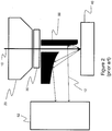
- Figure 1 shows a standard electron microscope with a direct detection backscattered electron detector 30.
- the electron beam 10 is directed through the pole piece 20 and the detector 30 to the sample 40.
- Backscattered electrons 11 leave the surface of the sample 20 and are detected by the detector 30.
- the detector is a direct electron detector as opposed to a detector comprising a scintillator that converts electrons to photons.
- FIG. 2 shows a prior art system for detecting cathodoluminescence photons 14 produced in the sample 40.
- a photon collection mirror 50 is placed between the backscattered electron detector 30 and the sample 40. Photons 12 produced by the sample 40 are directed by the mirror 50 to a photon detector 52.
- This configuration has the disadvantage that the mirror blocks a significant portion of the backscattered electrons from reaching the detector 30.
- a semiconductor diode 60 for sensing backscattered electrons 11 e.g. a silicon photodiode/avalanche diode
- a reflective coating applied to the diode 60 increases the reflectivity of the diode. Reflective coatings include aluminum and gold.
- the diode 60 has a three dimensional concave surface 61, such as an ellipsoidal or paraboloidal surface. This type of surface collimates or focuses the photons 12 onto other optical instrumentation, which can also include a conduit of the light to an external photon detector, (e.g. PMT or photodiode, or it can be the actual detector itself).
- an external photon detector e.g. PMT or photodiode, or it can be the actual detector itself.
- a miniature backscattered electron detector 70 is mounted within a photon directing element 80. Mounting the detector 70 close to the reflective plane of the optical element 80 means that the detector functions at a short working distance, compensating for the reduction in size by maintaining a large solid angle for the detector 70. Use of a miniature backscattered electron detector minimizes solid angle loss of the photon collection optical element 80. If a concave optical element (e.g. paraboloidal or ellipsoidal) is used, angling of the backscattered electron detector to reflect photons towards the photon detector minimizes optical losses as a result of the sacrificed solid angle of the optical element.
- a concave optical element e.g. paraboloidal or ellipsoidal
- the optical element 80 is made from conductive but highly reflective material e.g. diamond-turned aluminum.
- the backscattered electron detector is a silicon diode supported on a carrier for physical support.
Landscapes
- Chemical & Material Sciences (AREA)
- Analytical Chemistry (AREA)
- Analysing Materials By The Use Of Radiation (AREA)
Description
- This invention relates to image detectors for electron microscopy. In particular the invention relates to simultaneous detection of backscattered electrons and cathodoluminescence emitted by a sample.
- When a high energy electron or ion beam strikes a sample, photons can be emitted. These emitted photons are also known as cathodoluminescence. The collection and detection of these photons in the wavelength range from UV through visible to IR, can provide a wealth of information about the sample under investigation. However, the signal to be detected can be small and in order to obtain the highest signal to noise ratio, minimize acquisition times and reduce the excitation energy required it is desirable to collect the largest proportion of emitted photons as possible. The most efficient manner of collecting photons emitted from a sample in an electron microscope is by using an optical element which subtends a large solid angle and which detects the photons directly or directs the photons towards a light sensitive element where the photons can be detected and measured; typically, the optical element contains an aperture through which the incident primary electron beam may pass.
- Where the optical element used to direct the emitted photons covers such a large solid angle the use of other detectors simultaneously is compromised unless line of sight is provided by sacrificing the solid angle subtended by the optical element. A large solid angle is often required as the photon signal levels is typically many orders of magnitude lower than other signals in the SEM. For many signals in the SEM this is acceptable however, this is not the case for backscattered electrons for several reasons:
- 1) The emission direction of backscattered electrons and photons is similar and therefore collectors/detectors are required to occupy the same space. Therefore, a large sacrifice in both signals is required so that they may be sensed simultaneously. Backscattered electron detectors are typically mounted to the bottom of the pole piece or inserted immediately below, and the optical element used to direct photons is typically situated between the sample and the backscattered detector, thus obscuring the signal to the back scattered electron detector.
- 2) Sacrificing part of the optical element's solid angle allows the backscattered detector line of sight to the sample, however the optical element is typically thick (4 - 20mm) and the distance between the sample and the backscattered detector large therefore further compromising the solid angle subtended by the backscattered detector in comparison to normal operation.
- Detection of photons and backscattered electrons simultaneously is not novel; however, this has only been achieved through large sacrifices in efficiency - typically greater than or equal to 50% reduction in comparison to optimum operation of either detector. This is often unacceptable for many applications. Furthermore, this has only been achieved by the use of two separate instruments.
- Publications in the general field include
U.S. Patent nos. 7,462,839 and7,707,041 and Japanese Patent Abstract publication no. 11,096,956 by Hiromasa. - In an exemplary embodiment, the invention comprises an apparatus for detection of backscattered electrons and photons from a sample, comprising: a direct detection backscattered electron detector; and a photon detector; characterized in that said backscattered electron detector comprises a reflective surface that reflects photons emitted by the sample onto said photon detector. In an optional further embodiment, there is presented the apparatus as herein previously, wherein said reflective surface of said backscattered electron detector is convex. In another further embodiment, there is presented the apparatus as in the first embodiment, wherein said reflective surface of said backscattered electron detector is a three dimensional concave surface. In yet another further embodiment, there is presented the apparatus as in the previous embodiment, wherein said reflective surface is selected from the three dimensional geometric group consisting of an ellipsoidal surface and a paraboloidal surface.In another further embodiment, there is presented the apparatus as in the first embodiment, wherein said reflective surface is selected from the group consisting of aluminum and gold.
- In yet another further embodiment there is presented the apparatus as in the first embodiment also comprising: an optical element; wherein said backscattered electron detector is affixed within said optical element. Further to this embodiment previously described there is optionally presented apparatus wherein said backscattered electron detector is removably affixed within said optical element. Again, further to this embodiment there is provided an apparatus wherein said optical element is a concave reflector and wherein a primary electron beam passes through said backscattered electron detector and wherein said optical element directs the photons at an approximately 90 degree angle to said primary electron beam. Yet again, further to this embodiment there is provided an apparatus wherein said optical element is wherein said reflector is selected from the three dimensional geometric group consisting of an ellipsoidal surface and a paraboloidal surface. Yet again, further to this embodiment there is provided an apparatus wherein said optical element is a planar reflector. Yet again, further to this embodiment there is provided an apparatus wherein said backscattered electron detector is angled to reflect photons toward said photon detector.
- Further to those previously presented embodiments there is presented an apparatus for simultaneous detection of backscattered electrons and photons from a sample. The device includes a direct detection backscattered electron detector and a photon detector. The backscattered electron detector has a reflective surface that reflects photons emitted by the sample onto the photon detector. In an embodiment, the reflective surface is convex. In a further embodiment, the reflective surface is planar. In a further embodiment, the reflective surface of the backscattered electron detector is convex. In a further embodiment, the reflective surface of the backscattered electron detector is a three dimensional concave surface. Exemplary reflective surfaces include aluminum and gold
- In a further embodiment the apparatus includes a direct detection backscattered electron detector, a photon detector; and an optical element. In this embodiment, the backscattered electron detector is embedded in the optical element and is angled to reflect photons toward the photon detector.
- Other advantages and novel features of the invention will become apparent to those skilled in the art upon examination of the following detailed description of a preferred embodiment of the invention and the accompanying drawings.
-
-
Fig. 1 . is a diagram of a prior art electron microscope to detect backscattered electrons; -
Fig. 2 is a diagram of a prior art electron microscope to detect backscattered electrons and photons -
Fig. 3 is a diagram of an electron microscope to simultaneously detect backscattered electrons and photons, wherein the backscattered electron detector has a convex mirrored surface to reflect photons ; -
Fig. 4 is a diagram of an electron microscope to simultaneously detect backscattered electrons and cathodoluminesence, wherein the backscattered electron detector has a concave mirrored surface to reflect photons; and -
Fig. 5 is a diagram of a further embodiment of an electron microscope to simultaneously detect backscattered electrons and cathodoluminesence wherein a small backscattered electron detector is mounted in a photon directing element. -
Figure 1 shows a standard electron microscope with a direct detectionbackscattered electron detector 30. Theelectron beam 10 is directed through thepole piece 20 and thedetector 30 to thesample 40.Backscattered electrons 11 leave the surface of thesample 20 and are detected by thedetector 30. The detector is a direct electron detector as opposed to a detector comprising a scintillator that converts electrons to photons. -
Figure 2 shows a prior art system for detecting cathodoluminescence photons 14 produced in thesample 40. Aphoton collection mirror 50 is placed between thebackscattered electron detector 30 and thesample 40.Photons 12 produced by thesample 40 are directed by themirror 50 to aphoton detector 52. This configuration has the disadvantage that the mirror blocks a significant portion of the backscattered electrons from reaching thedetector 30. - In an embodiment of the invention shown in
Figure 3 , asemiconductor diode 60 for sensing backscattered electrons 11 (e.g. a silicon photodiode/avalanche diode) is shaped to directphotons 12 to anoptical detector 62. A reflective coating applied to thediode 60 increases the reflectivity of the diode. Reflective coatings include aluminum and gold. - In an alternate embodiment, shown in
Figure 4 , thediode 60 has a three dimensionalconcave surface 61, such as an ellipsoidal or paraboloidal surface. This type of surface collimates or focuses thephotons 12 onto other optical instrumentation, which can also include a conduit of the light to an external photon detector, (e.g. PMT or photodiode, or it can be the actual detector itself). - In a further embodiment, shown in
Figure 5 , a miniaturebackscattered electron detector 70 is mounted within aphoton directing element 80. Mounting thedetector 70 close to the reflective plane of theoptical element 80 means that the detector functions at a short working distance, compensating for the reduction in size by maintaining a large solid angle for thedetector 70. Use of a miniature backscattered electron detector minimizes solid angle loss of the photon collectionoptical element 80. If a concave optical element (e.g. paraboloidal or ellipsoidal) is used, angling of the backscattered electron detector to reflect photons towards the photon detector minimizes optical losses as a result of the sacrificed solid angle of the optical element. - In a further embodiment, the
optical element 80 is made from conductive but highly reflective material e.g. diamond-turned aluminum. - In a further embodiment, the backscattered electron detector is a silicon diode supported on a carrier for physical support.
Claims (11)
- An apparatus for detection of backscattered electrons (11) and photons (12) from a sample, comprising:a direct detection backscattered electron detector (60); anda photon detector (62);characterized in that said backscattered electron detector (60) comprises a reflective surface (61) that reflects photons (12) emitted by the sample onto said photon detector (62).
- The apparatus of Claim 1, wherein said reflective surface (61) of said backscattered electron detector (60) is convex.
- The apparatus of Claim 1, wherein said reflective surface (61) of said backscattered electron detector (60) is a three dimensional concave surface
- The apparatus of Claim 3, wherein said reflective surface (61) is selected from the three dimensional geometric group consisting of an ellipsoidal surface and a paraboloidal surface.
- The apparatus of Claim 1, wherein said reflective surface (61) is selected from the group consisting of aluminum and gold.
- The apparatus of claim 1 also comprising:an optical element (80);wherein said backscattered electron detector (60) is affixed within said optical element (80).
- The apparatus of claim 6 wherein said backscattered electron detector (60) is removably affixed within said optical element (80).
- The apparatus of Claim 6, wherein said optical element (80) is a concave reflector and wherein a primary electron beam (10) passes through said backscattered electron detector (60) and wherein said optical element (80) directs the photons (12) at an approximately 90 degree angle to said primary electron beam (10).
- The apparatus of Claim 8, wherein said concave reflector is selected from the three dimensional geometric group consisting of an ellipsoidal surface and a paraboloidal surface.
- The apparatus of Claim 6, wherein said optical element (80) is a planar reflector.
- The apparatus of Claim 6, wherein said backscattered electron detector (60) is angled to reflect photons (12) toward said photon detector (62).
Applications Claiming Priority (2)
| Application Number | Priority Date | Filing Date | Title |
|---|---|---|---|
| US13/280,952 US8410443B1 (en) | 2011-10-25 | 2011-10-25 | Integrated backscattered electron detector with cathodoluminescence collection optics |
| PCT/US2012/061538 WO2013063005A1 (en) | 2011-10-25 | 2012-10-24 | Integrated backscattered electron detector with cathodoluminescence collection optics |
Publications (2)
| Publication Number | Publication Date |
|---|---|
| EP2771900A1 EP2771900A1 (en) | 2014-09-03 |
| EP2771900B1 true EP2771900B1 (en) | 2017-04-19 |
Family
ID=47297408
Family Applications (1)
| Application Number | Title | Priority Date | Filing Date |
|---|---|---|---|
| EP12798051.4A Active EP2771900B1 (en) | 2011-10-25 | 2012-10-24 | Integrated backscattered electron detector with cathodoluminescence collection optics |
Country Status (4)
| Country | Link |
|---|---|
| US (1) | US8410443B1 (en) |
| EP (1) | EP2771900B1 (en) |
| JP (2) | JP6223985B2 (en) |
| WO (1) | WO2013063005A1 (en) |
Families Citing this family (7)
| Publication number | Priority date | Publication date | Assignee | Title |
|---|---|---|---|---|
| WO2015093465A1 (en) * | 2013-12-17 | 2015-06-25 | 株式会社堀場製作所 | Collector mirror, light/charged particle detection device, and sample analysis device |
| US10401374B2 (en) * | 2014-11-30 | 2019-09-03 | Tichauer Technical Laboratories, Llc | Device and method of detecting and generating combined modulated particle wave-fronts |
| US10055413B2 (en) | 2015-05-19 | 2018-08-21 | Spotify Ab | Identifying media content |
| US20180217059A1 (en) * | 2015-07-31 | 2018-08-02 | Fei Company | Segmented detector for a charged particle beam device |
| EP3792952B1 (en) * | 2019-09-16 | 2025-02-19 | FEI Company | Light guide assembly for an electron microscope |
| CN113675060A (en) * | 2020-05-13 | 2021-11-19 | 聚束科技(北京)有限公司 | Scanning electron microscope |
| CN113675061B (en) * | 2020-05-13 | 2024-09-06 | 聚束科技(北京)有限公司 | Scanning electron microscope |
Family Cites Families (14)
| Publication number | Priority date | Publication date | Assignee | Title |
|---|---|---|---|---|
| JPS517072B1 (en) * | 1970-10-23 | 1976-03-04 | ||
| IT1223998B (en) * | 1988-12-16 | 1990-09-29 | Sip | DETECTION SYSTEM FOR CATODOLUMINESCENCE ANALYSIS |
| JP3476482B2 (en) * | 1992-05-22 | 2003-12-10 | 株式会社トプコン | Morphological observation device |
| US5569920A (en) * | 1995-06-14 | 1996-10-29 | National University Of Singapore | Retractable cathodoluminescence detector with high ellipticity and high backscattered electron rejection performance for large area specimens |
| GB2314926B (en) * | 1996-07-01 | 1999-08-25 | K E Developments Ltd | Detector devices |
| JPH1196956A (en) | 1997-09-22 | 1999-04-09 | Hitachi Ltd | Scanning electron microscope |
| US7462839B2 (en) | 2000-07-07 | 2008-12-09 | Carl Zeiss Nts Gmbh | Detector for variable pressure areas and an electron microscope comprising a corresponding detector |
| US7707041B2 (en) | 2004-07-28 | 2010-04-27 | Conocophillips Company | Surface ownership data management system |
| EP1956633A3 (en) * | 2007-02-06 | 2009-12-16 | FEI Company | Particle-optical apparatus for simultaneous observing a sample with particles and photons |
| EP1956632A1 (en) * | 2007-02-14 | 2008-08-13 | FEI Company | Particle-optical apparatus for simultaneous observing a sample with particles and photons |
| JP2009170150A (en) * | 2008-01-11 | 2009-07-30 | Hitachi High-Technologies Corp | Inspection measurement device and inspection measurement method |
| US20100123077A1 (en) * | 2008-11-18 | 2010-05-20 | Gatan, Inc. | Passive pixel direct detection sensor |
| WO2010095392A1 (en) * | 2009-02-20 | 2010-08-26 | 株式会社日立ハイテクノロジーズ | Sample observing method and scanning electron microscope |
| JP5047318B2 (en) * | 2010-03-05 | 2012-10-10 | 株式会社日立ハイテクノロジーズ | Method for displaying an electron microscope image and an optical image in an overlapping manner |
-
2011
- 2011-10-25 US US13/280,952 patent/US8410443B1/en active Active
-
2012
- 2012-10-24 WO PCT/US2012/061538 patent/WO2013063005A1/en not_active Ceased
- 2012-10-24 EP EP12798051.4A patent/EP2771900B1/en active Active
- 2012-10-24 JP JP2014538894A patent/JP6223985B2/en active Active
-
2017
- 2017-05-01 JP JP2017091118A patent/JP6363253B2/en active Active
Non-Patent Citations (1)
| Title |
|---|
| None * |
Also Published As
| Publication number | Publication date |
|---|---|
| JP6223985B2 (en) | 2017-11-01 |
| JP2017188462A (en) | 2017-10-12 |
| JP2014531129A (en) | 2014-11-20 |
| US20130099116A1 (en) | 2013-04-25 |
| EP2771900A1 (en) | 2014-09-03 |
| US8410443B1 (en) | 2013-04-02 |
| JP6363253B2 (en) | 2018-07-25 |
| WO2013063005A1 (en) | 2013-05-02 |
Similar Documents
| Publication | Publication Date | Title |
|---|---|---|
| US8410443B1 (en) | Integrated backscattered electron detector with cathodoluminescence collection optics | |
| US20160313243A1 (en) | Particulate sensor device | |
| CN210166558U (en) | Microscope with high fluorescence collection rate | |
| CN107532940A (en) | Photoelectron device | |
| CN107462566B (en) | Raman spectrometer for detecting specific narrow wavenumber range | |
| CN106796861A (en) | Mixed tensor is changed and processing detection device | |
| RU2015144501A (en) | SURFACE RURGE MEASUREMENT DEVICE | |
| JP2017515270A5 (en) | Hybrid energy converter | |
| Armstrong et al. | The University of Durham mark 6 gamma ray telescope | |
| US5416325A (en) | Fourier transform infrared spectrometer | |
| US20210183614A1 (en) | Charged particle beam apparatus | |
| US9279889B2 (en) | Light detection unit and alpha ray observation device | |
| US20180217059A1 (en) | Segmented detector for a charged particle beam device | |
| ITBO20100361A1 (en) | OPTO-ELECTRONIC SYSTEM FOR RADIOMETRIC MEASUREMENTS. | |
| CN101571601A (en) | Photoelectonic sensor | |
| US8735837B2 (en) | Gamma camera system | |
| US8124925B2 (en) | Simulation detector having multiple sensor surfaces for detecting incident radiation | |
| CN101903795B (en) | Radiation sensor for detecting the position and intensity of a radiation source | |
| CN214954097U (en) | Imaging system | |
| JP4217788B2 (en) | Radiation arrival position detection method and apparatus | |
| US12584788B2 (en) | Optical power meter for safe operation of optical wireless power systems | |
| EP2716220B1 (en) | Digital image detector using a diffraction grating and detection method | |
| JP2010096716A (en) | Infrared camera | |
| US20080246872A1 (en) | System and method for improving performance of optical systems with tilted windows | |
| JP2008145213A (en) | THERMAL FLUCTUATION NOISE REDUCTION STRUCTURE FOR beta-RAY DETECTOR |
Legal Events
| Date | Code | Title | Description |
|---|---|---|---|
| PUAI | Public reference made under article 153(3) epc to a published international application that has entered the european phase |
Free format text: ORIGINAL CODE: 0009012 |
|
| 17P | Request for examination filed |
Effective date: 20140423 |
|
| AK | Designated contracting states |
Kind code of ref document: A1 Designated state(s): AL AT BE BG CH CY CZ DE DK EE ES FI FR GB GR HR HU IE IS IT LI LT LU LV MC MK MT NL NO PL PT RO RS SE SI SK SM TR |
|
| DAX | Request for extension of the european patent (deleted) | ||
| GRAP | Despatch of communication of intention to grant a patent |
Free format text: ORIGINAL CODE: EPIDOSNIGR1 |
|
| STAA | Information on the status of an ep patent application or granted ep patent |
Free format text: STATUS: GRANT OF PATENT IS INTENDED |
|
| RAP1 | Party data changed (applicant data changed or rights of an application transferred) |
Owner name: GATAN, INC. |
|
| INTG | Intention to grant announced |
Effective date: 20161108 |
|
| GRAS | Grant fee paid |
Free format text: ORIGINAL CODE: EPIDOSNIGR3 |
|
| GRAA | (expected) grant |
Free format text: ORIGINAL CODE: 0009210 |
|
| STAA | Information on the status of an ep patent application or granted ep patent |
Free format text: STATUS: THE PATENT HAS BEEN GRANTED |
|
| AK | Designated contracting states |
Kind code of ref document: B1 Designated state(s): AL AT BE BG CH CY CZ DE DK EE ES FI FR GB GR HR HU IE IS IT LI LT LU LV MC MK MT NL NO PL PT RO RS SE SI SK SM TR |
|
| REG | Reference to a national code |
Ref country code: GB Ref legal event code: FG4D |
|
| REG | Reference to a national code |
Ref country code: CH Ref legal event code: EP |
|
| REG | Reference to a national code |
Ref country code: AT Ref legal event code: REF Ref document number: 886679 Country of ref document: AT Kind code of ref document: T Effective date: 20170515 |
|
| REG | Reference to a national code |
Ref country code: IE Ref legal event code: FG4D |
|
| REG | Reference to a national code |
Ref country code: DE Ref legal event code: R096 Ref document number: 602012031408 Country of ref document: DE |
|
| REG | Reference to a national code |
Ref country code: NL Ref legal event code: FP |
|
| REG | Reference to a national code |
Ref country code: LT Ref legal event code: MG4D |
|
| REG | Reference to a national code |
Ref country code: AT Ref legal event code: MK05 Ref document number: 886679 Country of ref document: AT Kind code of ref document: T Effective date: 20170419 |
|
| REG | Reference to a national code |
Ref country code: FR Ref legal event code: PLFP Year of fee payment: 6 |
|
| PG25 | Lapsed in a contracting state [announced via postgrant information from national office to epo] |
Ref country code: ES Free format text: LAPSE BECAUSE OF FAILURE TO SUBMIT A TRANSLATION OF THE DESCRIPTION OR TO PAY THE FEE WITHIN THE PRESCRIBED TIME-LIMIT Effective date: 20170419 Ref country code: GR Free format text: LAPSE BECAUSE OF FAILURE TO SUBMIT A TRANSLATION OF THE DESCRIPTION OR TO PAY THE FEE WITHIN THE PRESCRIBED TIME-LIMIT Effective date: 20170720 Ref country code: FI Free format text: LAPSE BECAUSE OF FAILURE TO SUBMIT A TRANSLATION OF THE DESCRIPTION OR TO PAY THE FEE WITHIN THE PRESCRIBED TIME-LIMIT Effective date: 20170419 Ref country code: HR Free format text: LAPSE BECAUSE OF FAILURE TO SUBMIT A TRANSLATION OF THE DESCRIPTION OR TO PAY THE FEE WITHIN THE PRESCRIBED TIME-LIMIT Effective date: 20170419 Ref country code: AT Free format text: LAPSE BECAUSE OF FAILURE TO SUBMIT A TRANSLATION OF THE DESCRIPTION OR TO PAY THE FEE WITHIN THE PRESCRIBED TIME-LIMIT Effective date: 20170419 Ref country code: NO Free format text: LAPSE BECAUSE OF FAILURE TO SUBMIT A TRANSLATION OF THE DESCRIPTION OR TO PAY THE FEE WITHIN THE PRESCRIBED TIME-LIMIT Effective date: 20170719 Ref country code: LT Free format text: LAPSE BECAUSE OF FAILURE TO SUBMIT A TRANSLATION OF THE DESCRIPTION OR TO PAY THE FEE WITHIN THE PRESCRIBED TIME-LIMIT Effective date: 20170419 |
|
| PG25 | Lapsed in a contracting state [announced via postgrant information from national office to epo] |
Ref country code: RS Free format text: LAPSE BECAUSE OF FAILURE TO SUBMIT A TRANSLATION OF THE DESCRIPTION OR TO PAY THE FEE WITHIN THE PRESCRIBED TIME-LIMIT Effective date: 20170419 Ref country code: PL Free format text: LAPSE BECAUSE OF FAILURE TO SUBMIT A TRANSLATION OF THE DESCRIPTION OR TO PAY THE FEE WITHIN THE PRESCRIBED TIME-LIMIT Effective date: 20170419 Ref country code: SE Free format text: LAPSE BECAUSE OF FAILURE TO SUBMIT A TRANSLATION OF THE DESCRIPTION OR TO PAY THE FEE WITHIN THE PRESCRIBED TIME-LIMIT Effective date: 20170419 Ref country code: BG Free format text: LAPSE BECAUSE OF FAILURE TO SUBMIT A TRANSLATION OF THE DESCRIPTION OR TO PAY THE FEE WITHIN THE PRESCRIBED TIME-LIMIT Effective date: 20170719 Ref country code: LV Free format text: LAPSE BECAUSE OF FAILURE TO SUBMIT A TRANSLATION OF THE DESCRIPTION OR TO PAY THE FEE WITHIN THE PRESCRIBED TIME-LIMIT Effective date: 20170419 Ref country code: IS Free format text: LAPSE BECAUSE OF FAILURE TO SUBMIT A TRANSLATION OF THE DESCRIPTION OR TO PAY THE FEE WITHIN THE PRESCRIBED TIME-LIMIT Effective date: 20170819 |
|
| REG | Reference to a national code |
Ref country code: DE Ref legal event code: R097 Ref document number: 602012031408 Country of ref document: DE |
|
| PG25 | Lapsed in a contracting state [announced via postgrant information from national office to epo] |
Ref country code: SK Free format text: LAPSE BECAUSE OF FAILURE TO SUBMIT A TRANSLATION OF THE DESCRIPTION OR TO PAY THE FEE WITHIN THE PRESCRIBED TIME-LIMIT Effective date: 20170419 Ref country code: DK Free format text: LAPSE BECAUSE OF FAILURE TO SUBMIT A TRANSLATION OF THE DESCRIPTION OR TO PAY THE FEE WITHIN THE PRESCRIBED TIME-LIMIT Effective date: 20170419 Ref country code: RO Free format text: LAPSE BECAUSE OF FAILURE TO SUBMIT A TRANSLATION OF THE DESCRIPTION OR TO PAY THE FEE WITHIN THE PRESCRIBED TIME-LIMIT Effective date: 20170419 Ref country code: EE Free format text: LAPSE BECAUSE OF FAILURE TO SUBMIT A TRANSLATION OF THE DESCRIPTION OR TO PAY THE FEE WITHIN THE PRESCRIBED TIME-LIMIT Effective date: 20170419 |
|
| PLBE | No opposition filed within time limit |
Free format text: ORIGINAL CODE: 0009261 |
|
| STAA | Information on the status of an ep patent application or granted ep patent |
Free format text: STATUS: NO OPPOSITION FILED WITHIN TIME LIMIT |
|
| PG25 | Lapsed in a contracting state [announced via postgrant information from national office to epo] |
Ref country code: IT Free format text: LAPSE BECAUSE OF FAILURE TO SUBMIT A TRANSLATION OF THE DESCRIPTION OR TO PAY THE FEE WITHIN THE PRESCRIBED TIME-LIMIT Effective date: 20170419 Ref country code: SM Free format text: LAPSE BECAUSE OF FAILURE TO SUBMIT A TRANSLATION OF THE DESCRIPTION OR TO PAY THE FEE WITHIN THE PRESCRIBED TIME-LIMIT Effective date: 20170419 |
|
| 26N | No opposition filed |
Effective date: 20180122 |
|
| PG25 | Lapsed in a contracting state [announced via postgrant information from national office to epo] |
Ref country code: SI Free format text: LAPSE BECAUSE OF FAILURE TO SUBMIT A TRANSLATION OF THE DESCRIPTION OR TO PAY THE FEE WITHIN THE PRESCRIBED TIME-LIMIT Effective date: 20170419 Ref country code: MC Free format text: LAPSE BECAUSE OF FAILURE TO SUBMIT A TRANSLATION OF THE DESCRIPTION OR TO PAY THE FEE WITHIN THE PRESCRIBED TIME-LIMIT Effective date: 20170419 |
|
| REG | Reference to a national code |
Ref country code: IE Ref legal event code: MM4A |
|
| PG25 | Lapsed in a contracting state [announced via postgrant information from national office to epo] |
Ref country code: LU Free format text: LAPSE BECAUSE OF NON-PAYMENT OF DUE FEES Effective date: 20171024 |
|
| REG | Reference to a national code |
Ref country code: BE Ref legal event code: MM Effective date: 20171031 |
|
| PG25 | Lapsed in a contracting state [announced via postgrant information from national office to epo] |
Ref country code: BE Free format text: LAPSE BECAUSE OF NON-PAYMENT OF DUE FEES Effective date: 20171031 |
|
| PG25 | Lapsed in a contracting state [announced via postgrant information from national office to epo] |
Ref country code: MT Free format text: LAPSE BECAUSE OF NON-PAYMENT OF DUE FEES Effective date: 20171024 |
|
| PG25 | Lapsed in a contracting state [announced via postgrant information from national office to epo] |
Ref country code: IE Free format text: LAPSE BECAUSE OF NON-PAYMENT OF DUE FEES Effective date: 20171024 |
|
| REG | Reference to a national code |
Ref country code: FR Ref legal event code: PLFP Year of fee payment: 7 |
|
| PG25 | Lapsed in a contracting state [announced via postgrant information from national office to epo] |
Ref country code: HU Free format text: LAPSE BECAUSE OF FAILURE TO SUBMIT A TRANSLATION OF THE DESCRIPTION OR TO PAY THE FEE WITHIN THE PRESCRIBED TIME-LIMIT; INVALID AB INITIO Effective date: 20121024 |
|
| PG25 | Lapsed in a contracting state [announced via postgrant information from national office to epo] |
Ref country code: CY Free format text: LAPSE BECAUSE OF NON-PAYMENT OF DUE FEES Effective date: 20170419 |
|
| PG25 | Lapsed in a contracting state [announced via postgrant information from national office to epo] |
Ref country code: MK Free format text: LAPSE BECAUSE OF FAILURE TO SUBMIT A TRANSLATION OF THE DESCRIPTION OR TO PAY THE FEE WITHIN THE PRESCRIBED TIME-LIMIT Effective date: 20170419 |
|
| PG25 | Lapsed in a contracting state [announced via postgrant information from national office to epo] |
Ref country code: TR Free format text: LAPSE BECAUSE OF FAILURE TO SUBMIT A TRANSLATION OF THE DESCRIPTION OR TO PAY THE FEE WITHIN THE PRESCRIBED TIME-LIMIT Effective date: 20170419 |
|
| PG25 | Lapsed in a contracting state [announced via postgrant information from national office to epo] |
Ref country code: PT Free format text: LAPSE BECAUSE OF FAILURE TO SUBMIT A TRANSLATION OF THE DESCRIPTION OR TO PAY THE FEE WITHIN THE PRESCRIBED TIME-LIMIT Effective date: 20170419 |
|
| PG25 | Lapsed in a contracting state [announced via postgrant information from national office to epo] |
Ref country code: AL Free format text: LAPSE BECAUSE OF FAILURE TO SUBMIT A TRANSLATION OF THE DESCRIPTION OR TO PAY THE FEE WITHIN THE PRESCRIBED TIME-LIMIT Effective date: 20170419 |
|
| P01 | Opt-out of the competence of the unified patent court (upc) registered |
Effective date: 20230615 |
|
| REG | Reference to a national code |
Ref country code: CH Ref legal event code: U11 Free format text: ST27 STATUS EVENT CODE: U-0-0-U10-U11 (AS PROVIDED BY THE NATIONAL OFFICE) Effective date: 20251101 |
|
| PGFP | Annual fee paid to national office [announced via postgrant information from national office to epo] |
Ref country code: NL Payment date: 20251023 Year of fee payment: 14 |
|
| PGFP | Annual fee paid to national office [announced via postgrant information from national office to epo] |
Ref country code: DE Payment date: 20251020 Year of fee payment: 14 |
|
| PGFP | Annual fee paid to national office [announced via postgrant information from national office to epo] |
Ref country code: GB Payment date: 20251029 Year of fee payment: 14 |
|
| PGFP | Annual fee paid to national office [announced via postgrant information from national office to epo] |
Ref country code: FR Payment date: 20251022 Year of fee payment: 14 |
|
| PGFP | Annual fee paid to national office [announced via postgrant information from national office to epo] |
Ref country code: CH Payment date: 20251101 Year of fee payment: 14 |
|
| PGFP | Annual fee paid to national office [announced via postgrant information from national office to epo] |
Ref country code: CZ Payment date: 20251013 Year of fee payment: 14 |