EP2764618B1 - Filteranordnung - Google Patents
Filteranordnung Download PDFInfo
- Publication number
- EP2764618B1 EP2764618B1 EP12758447.2A EP12758447A EP2764618B1 EP 2764618 B1 EP2764618 B1 EP 2764618B1 EP 12758447 A EP12758447 A EP 12758447A EP 2764618 B1 EP2764618 B1 EP 2764618B1
- Authority
- EP
- European Patent Office
- Prior art keywords
- signal
- filter
- transmit
- output
- port
- Prior art date
- Legal status (The legal status is an assumption and is not a legal conclusion. Google has not performed a legal analysis and makes no representation as to the accuracy of the status listed.)
- Not-in-force
Links
- 230000002457 bidirectional effect Effects 0.000 claims description 18
- 238000001914 filtration Methods 0.000 claims description 18
- 238000004519 manufacturing process Methods 0.000 claims description 7
- 238000004590 computer program Methods 0.000 claims description 3
- 230000006870 function Effects 0.000 claims description 3
- 230000001419 dependent effect Effects 0.000 claims description 2
- 238000013461 design Methods 0.000 description 8
- 238000000034 method Methods 0.000 description 5
- 238000003780 insertion Methods 0.000 description 4
- 230000037431 insertion Effects 0.000 description 4
- 238000010295 mobile communication Methods 0.000 description 4
- 239000000919 ceramic Substances 0.000 description 3
- 230000005540 biological transmission Effects 0.000 description 2
- 238000005516 engineering process Methods 0.000 description 2
- 230000003287 optical effect Effects 0.000 description 2
- 239000004065 semiconductor Substances 0.000 description 2
- 239000003990 capacitor Substances 0.000 description 1
- 238000004891 communication Methods 0.000 description 1
- 230000001066 destructive effect Effects 0.000 description 1
- 230000002542 deteriorative effect Effects 0.000 description 1
- 230000000694 effects Effects 0.000 description 1
- 238000012545 processing Methods 0.000 description 1
- 230000001681 protective effect Effects 0.000 description 1
- 230000006798 recombination Effects 0.000 description 1
- 238000005215 recombination Methods 0.000 description 1
- 230000035945 sensitivity Effects 0.000 description 1
- 238000004088 simulation Methods 0.000 description 1
- 235000013599 spices Nutrition 0.000 description 1
- 230000001629 suppression Effects 0.000 description 1
- 238000010897 surface acoustic wave method Methods 0.000 description 1
- 238000012360 testing method Methods 0.000 description 1
Images


Classifications
-
- H—ELECTRICITY
- H03—ELECTRONIC CIRCUITRY
- H03H—IMPEDANCE NETWORKS, e.g. RESONANT CIRCUITS; RESONATORS
- H03H9/00—Networks comprising electromechanical or electro-acoustic elements; Electromechanical resonators
- H03H9/46—Filters
- H03H9/54—Filters comprising resonators of piezoelectric or electrostrictive material
-
- H—ELECTRICITY
- H03—ELECTRONIC CIRCUITRY
- H03H—IMPEDANCE NETWORKS, e.g. RESONANT CIRCUITS; RESONATORS
- H03H7/00—Multiple-port networks comprising only passive electrical elements as network components
- H03H7/01—Frequency selective two-port networks
Definitions
- the field of the present application relates in general to a filter arrangement and in particular to a radio station with a filter arrangement.
- the field of the application also relates to a method of manufacturing a filter arrangement.
- Filters are designed, for example, for a specific frequency band. Signals within that specific frequency band will pass the filter from a first port to a second port whereas signals outside of the specific frequency band will be prevented from passing through the filter.
- the filters may be produced as a combination of resistors, inductors, and capacitors or as ceramic filters, such as but not limited to surface acoustic wave filters or film bulk acoustic resonators. Dependent on their technology each filter may be distinguishable from other filters by electrical characteristics such as insertion loss, out-band signal rejection, electric power durability, but also in size and price.
- a special application of filters is a duplex filter for radio transceivers.
- a duplex filter enables a transmitter and a receiver to share a single antenna, by preventing a transmission signal from entering the receiver and, likewise, the received signal from entering the transmitter.
- the duplex filter usually comprises two separate band-pass filters, one of which is connected to the receiver section of the transceiver, and the other filter being connected to the transmitter section of the transceiver.
- Duplex filter designs are commercially available as off-the-shelf filters for a plurality of different circuit designs for the transceiver. However, the technical properties of these off-the-shelf filters may not always meet the design criteria a circuit designer has in mind when designing a radio station.
- Document WO 95/28746 and document WO 2013/011026 which is an intermediate document under Article 54(3) EPC, describe a filter arrangement for filtering a radio signal comprising at least one first filter stage, the at least one first filter stage comprising a divide stage for dividing a filter stage input signal into at least a first signal portion, and at least a second signal portion, wherein the at least a first signal portion is passed to at least a first divide stage output and the at least a second signal portion is passed to a at least second divide stage output, at least a first filter element comprising a first filter element input being connected to the first divide stage output and a first filter element output for providing at least a first filtered signal, at least a second filter element comprising a second filter element input being connected to the second divide stage output and a second filter element output for providing at least a second filtered signal, and a combine stage for combining the first filtered signal, received at the first combine stage input and the second filtered signal, received at the second signal combiner input into a filter
- the present invention proposes a duplex filter arrangement according to claim 1.
- Another aspect of the teaching of this application is to provide a chipset according to claim 14
- Another aspect of the teaching of this application is a radio station according to claim 15.
- Fig. 1 shows a first aspect of a filter arrangement 1 according to the present disclosure and not part of the claimed invention for filtering a filter arrangement input signal 101 received at a filter arrangement input 102 and providing a filter arrangement output signal 104 at a filter arrangement output 103.
- the filter arrangement input signal may be but is not limited to a transmit signal or a receive signal.
- a plurality of transmit signals use adjacent frequencies and form a transmit band.
- a plurality of receive signals use adjacent frequencies and form a receive band.
- the transmit band and the receive band are distinct to each other.
- the filter arrangement input signal 101 is first passed through a divide stage 200 wherein the filter arrangement input signal 101 is split up into a first and a second divide stage output signal which are provided at a first signal divide stage output 201 and a second divide stage output 202.
- the first filter stage output signal and the second filter stage output signals pass each through a first filter element 310 and a second filter element 320 which constitute a first filter element stage 300, producing a first filter stage output signal and a second filter stage output signal.
- a combine stage 400 the first filter element stage output signal and the second filter element stage output signal, received respectively at a first filter combine stage input 401 and a second filter combine stage input 402 are combined into a first combine stage signal, which is provided at a first combine stage output 409.
- the first combine stage output coincides with the first filter arrangement output 103.
- the filter elements may be, but are not limited to band pass filters for a transmitting band or band pass filter for a receiving band.
- the divide stage 200 is formed by a first signal divider 210.
- the first signal divider 210 is connected to the first divide stage input 102.
- the first signal divider 210 splits a first signal divider input signal received at the first signal divider input 211 into a first portion and a second portion of the signal divider input signal.
- the first portion of the signal divider input signal is provided at a first signal divider output 212, which forms the first divide stage output 201.
- the second portion of the signal divider input signal is provided at a second signal divider output 213, which forms the second divide stage output 202.
- the first divide stage output 201 is connected to a first filter element input 311 of the first filter element 310, whereas the second divide stage output 202 is connected to a second filter element input 321 of the second filter element 320.
- the combine stage 400 is formed by a first signal combiner 410 comprising a first signal combiner input 411 and a second signal combiner input 412.
- the first signal combiner input 411 coincides with the first combine stage input 401 and the second signal combiner input 412 coincides with the second combine stage input 402.
- the first filter element output 312 of the first filter element 310 is connected to the first signal combiner input 411 of the first signal combiner 410 and the second filter element output 322 of the second filter element 320 is connected to the second signal combiner input 412 of the first signal combiner 410.
- the first signal combiner 410 combines the input signals at the first signal combiner input 411 and the second combiner input 412 into a first signal combiner output signal, which is provided at a signal combiner output 413.
- the signal combiner output 413 coincides in this aspect of the disclosure with the filter stage output 103
- the signal combiner output signal constitutes in this aspect of the present disclosure a filter stage output signal of the filter stage 1 as well as the filter arrangement output signal 104.
- each one of the first filter element 310 and the second filter element 320 have to carry only half of the power of the filter arrangement input signal 101.
- the filter stage 300 can be designed for a twice as high power durability than each of the separate first filter element 310 and the second filter elements 320 is specified for.
- Some filter characteristics of the filter stage 300 are not affected by the parallel-arranged first filter element 310 and second filter element 320, if losses in the first signal divider 210 and in the first signal combiner 410 are neglected.
- the insertion loss e.g. the attenuation of a signal that passes the filter stage 300 is independent of the number of parallel-arranged filter elements 310, 320.
- the signal delay through the first filter element 310 and the second filter element 320 should be within a certain tolerance limit in order to ensure that the output power at the first filter arrangement output 103 is not significantly degraded.
- a filter stage 300 may also comprise more than two parallel filter elements 310, 320.
- Signal divider with multiple output signals and signal combiner with multiple inputs are part of the state of the art and may be chosen accordingly to use a plurality of parallel filter elements in one filter stage. The power of the filter arrangement signal can be distributed accordingly.
- Fig. 2 shows a second aspect not part of the claimed invention of a filter arrangement 1 according to the present disclosure, wherein the filter arrangement 1 again comprises a divide stage 200, a filter stage 300 and a combine stage 400.
- the divide stage 200 splits the first filter arrangement input signal 101 into a first filter stage output signal, a second filter stage output signal, a third filter stage output signal and a fourth filter stage output signal which are provided at a first divide stage output 201, a second divide stage output 202, a third divide stage output 203 and a fourth divide stage output 204.
- the filter stage 300 comprises consequently four separate filter elements, a first filter element 310, a second filter element 320, a third filter element 330 and a fourth filter element 340.
- a first filter element output signal from the first filter element 310 is passed to a first combine stage input 401.
- a second filter element output signal from the second filter element 320 is passed to a second combine stage input 402.
- a third filter element output signal from the third filter element 330 is passed to a third combine stage input 403 and a fourth filter element output signal from the fourth filter element 340 is passed to a fourth combine stage input 404.
- the combine stage 400 combines a first combine stage input signal received at the first combine stage input 401, a second combine stage input signal received at the second combine signal stage input 402, a third combine stage input signal received at the third combine stage input 403 and a fourth combine stage input signal received at the fourth combine stage input 404 into a combine stage output signal which is passed to a combine stage output 409 which coincides in this aspect of the present disclosure with the filter arrangement output 103.
- the divide stage 200 is formed by a first signal divider 210, a second signal divider 220 and a third signal divider 230.
- a first signal divider input 211 is identical to the first combine stage input 102.
- the first signal divider 210 splits a first signal divider input signal, received at the first signal divider input 211 into a first portion and a second portion of the first signal divider input signal.
- the first portion of the first signal divider input signal is provided at a first signal divider output 212 and the second portion of the first signal divider input signal is provided at a second signal divider output 213.
- the first signal divider output 212 is connected to a second signal divider input 221 of the second signal divider 220 and the second signal divider output 213 is connected to a third signal divider input 231 of the third signal divider 230.
- the second signal divider 220 splits a second signal divider input signal, received at the second signal divider input 221 into a third portion and a fourth portion of the second signal divider input signal.
- the third portion of the second signal divider input signal is provided at a third signal divider output 222, which is in this aspect of the present disclosure identical to the divide stage output 201.
- the fourth portion of the second signal divider input signal is provided at a fourth signal divider output 223, which is in this aspect of the present disclosure identical to the second divide stage output 202.
- the third signal divider 230 splits a third signal divider input signal, received at the third signal divider input 231 into a fifth portion and a sixth portion of the third signal divider input signal.
- the fifth portion of the third signal divider input signal is provided at a fifth signal divider output 232, which is in this aspect of the present disclosure identical to the third divide stage output 203.
- the sixth portion of the third signal divider input signal is provided at a sixth signal divider output 233, which is in this aspect of the present disclosure identical to the fourth divide stage output 204.
- the combine stage 400 comprises a first signal combiner 410, a second signal combiner 420 and a third signal combiner 430.
- the first combine stage input 401 is connected to a third signal combiner input 421 of the second signal combiner 420
- the second combine stage input 402 is connected to a fourth signal combiner input 422 of the second signal combiner 420.
- the second signal combiner 420 combines the third input signal and the fourth input signal received at the third signal combiner input 421 and the fourth signal combiner input 422 into a second signal combiner output signal, which is provided at a second signal combiner output 423.
- the third combine stage input 403 is connected to a fifth signal combiner input 431 of the third signal combiner 430, and the fourth combine stage input 404 is connected to a sixth signal combiner input 432 of the third signal combiner 430.
- the third signal combiner 430 combines the fifth input signal and the sixth input signal received at the fifth signal combiner input 431 and the sixth signal combiner input 432 into a third single signal combiner output signal which is provided at a third signal combiner output 433.
- the second signal combiner output 423 is connected to a first signal combiner input 411 of the first signal combiner 410, and the third signal combiner output 433 is connected to a second signal combiner input 412 of the first signal combiner 410.
- the first signal combiner 410 combines the first input signal and the second input signal received at the first signal combiner input 411 and the second signal combiner input 412 into a first single signal combiner output signal which is provided at a first signal combiner output 413.
- the first single signal combiner output signal forms in this aspect of the present disclosure the output signal of the combine stage 400 and thereby forms the filter arrangement output signal 104.
- the four filter elements (the first filter element 310, the second filter element 320, the third filter element 330 and the fourth filter element 340) are used in parallel. If each of the first signal divider 210, the second signal divider 220 and third signal divider 230 splits the power of each of the first signal divider input signal, the second signal divider input signal and the third signal divider input signal in two equal power portions, each one of the filter elements is charged only with a fourth of the power of the filter arrangement input signal 101.
- the filter arrangement output signal 104 is again at the power level of the filter arrangement input signal 101.
- each signal divider splits an input signal into two signal portions
- each signal divider may be chosen to split a signal divider input signal into a number of signal portions greater than two.
- Fig. 3 shows a third aspect not part of the claimed invention of the filter arrangement 1 according to the present disclosure, wherein a divide stage 200 is formed by a first signal divider 210, a second signal divider 220, a third signal divider 230, a fourth signal divider 240, a fifth signal divider 250, a sixth signal divider 260 and a seventh signal divider 270.
- the arrangement of the first signal divider 210, the second signal divider 220 and the third signal divider 230 is identical to the arrangement of the first signal divider 210, the second signal divider 220 and the third signal divider 230 described in the second aspect of the present disclosure, to which is made reference here.
- the third signal divider output 222 in the third aspect of the present disclosure is connected to a fourth signal divider input 241 of the fourth signal combiner 240.
- the fourth signal divider output 223 is connected to a fifth signal divider input 251 of the fifth signal combiner 250
- the fifth signal combiner output 232 is connected to a sixth signal combiner input 261 of the sixth signal combiner 260
- the sixth signal divider output 233 is connected to a seventh signal combiner input 271 of the seventh signal divider 270.
- a seventh signal divider output 242 of the fourth signal divider 240 forms the first divide stage output 201 of the divide stage 200; a eighth signal divider output 243 of the fourth signal divider 240 forms the second divide stage output 202 of the divide stage 200; a ninth signal divider output 252 of the fifth signal divider 250 forms the third divide stage output 203 of the divide stage 200; a tenth signal divider output 253 of the fifth signal divider 250 forms the fourth divide stage output 204 of the divide stage 200; a eleventh signal divider output 262 of the sixth signal divider 260 forms the fifth divide stage output 205 of the divide stage 200; a twelfth signal divider output 263 of the sixth signal divider 260 forms the sixth divide stage output 206 of the divide stage 200; a thirteenth signal divider output 272 of the seventh signal divider 270 forms the seventh divide stage output 207 of the divide stage 200; and a fourteenth signal divider output 273 of the seventh signal divider 270 forms the eighth divide stage output 208 of the divide stage 200
- a first combine stage input 401 is connected to a seventh signal combiner input 441 of a fourth signal combiner 440; a second combine stage input 402 is connected to an eighth signal combiner input 442 of the fourth signal combiner 440; a third combine stage input 403 is connected to a ninth signal combiner input 451 of a fifth signal combiner 450; a fourth combine stage input 404 is connected to a tenth signal combiner input 452 of the fifth signal combiner 450; a fifth combine stage input 405 is connected to an eleventh signal combiner input 461 of a sixth signal combiner 460; a sixth combine stage input 406 is connected to a twelfth signal combiner input 462 of the sixth signal combiner 460; a seventh combine stage input 407 is connected to a thirteenth signal combiner input 471 of a seventh signal combiner 470; a eighth combine stage input 408 is
- a fourth signal combiner output 443 of the fourth signal combiner 440 is connected to a third signal combiner input 421 of the second signal combiner 420 and a fifth signal combiner output 453 of the fifth signal combiner 450 is connected to a fourth signal combiner input 422 of the second signal combiner 420.
- a sixth signal combiner output 463 of the sixth signal combiner 460 is connected to a fifth signal combiner input 431 of the third signal combiner 430; and a seventh signal combiner output 473 of the seventh signal combiner 470 is connected to a sixth signal combiner input 432 of the third signal combiner 430.
- a second signal combiner output 423 of the second signal combiner 420 is connected to a first signal combiner input 411 of the first signal combiner 410 and a third signal combiner output 433 of the third signal combiner 430 is connected to a second signal combiner input 412 of the first signal combiner 410.
- the first signal combiner output 413 of the first signal combiner 410 forms the output 103 of the filter arrangement 1.
- the power of the filter arrangement input signal 101 is equally split into eight separate portion signals which are passed through a first filter element 310, a second filter element 320, a third filter element 330, a fourth filter element 340, a fifth filter element 350, a sixth filter element 360, a seventh filter element 370, and an eighth filter element 380 of the filter stage 300.
- a first filter element 310 a second filter element 320, a third filter element 330, a fourth filter element 340, a fifth filter element 350, a sixth filter element 360, a seventh filter element 370, and an eighth filter element 380 of the filter stage 300.
- FBAR film bulk acoustic resonator filter
- Bulk acoustic resonator filters are piezoelectric filters, which are far smaller than other types of filters, like ceramic filters or surface acoustic resonators (SAW).
- SAW surface acoustic resonators
- their use in transceivers has been limited to transceivers with a maximum output power of +30 dBm.
- a typical miniature PCS/UMTS Band pass filter is available at the time of the present disclosure from AVAGO technologies under the product name ACMD-7005.
- the data sheet of this band pass filter shows a high power rating of +30dBm.
- this filter arrangement can be used in transceivers with an output power of +39 dBm, as each doubling of the number of parallel arranged filter elements adds an additional power durability of +3dbm (e.g. distributing the power on two filter elements increases the maximum output power by +3dB, distributing the power on four filter elements increases the maximum output power by +6dB, distributing the power on eight filter elements increases the maximum output power by +9dB compared to a single filter element).
- +3dbm e.g. distributing the power on two filter elements increases the maximum output power by +3dB
- distributing the power on four filter elements increases the maximum output power by +6dB
- distributing the power on eight filter elements increases the maximum output power by +9dB compared to a single filter element.
- FIG. 4 shows a filter arrangement not part of the claimed invention with a divide stage 200, a first duplex filter 510 and a second duplex filter 520 and a combine stage 400. Apart from the first duplex filter 510 and the second duplex filter 520 this filter arrangement is identical to the filter arrangement described in Fig. 1 of the present disclosure.
- the first divide stage output 201 of the divide stage 200 is connected to a first transmit port 511 of the first duplex filter 510.
- a first antenna port 513 of the first duplex filter 510 is connected to a first combine stage input 401 of the combine stage 400.
- a first receive port 512 of the duplex filter 510 is connected via a load impedance 514 to a reference level.
- the second divide stage output 202 of the divide stage 200 is connected to the second transmit port 521 of the second duplex-filter 520.
- the second antenna port 523 of the second duplex-filter 520 is connected to the second combine stage input 402 of the second signal combiner 400.
- a second receive port 522 of the second duplex filter 520 is connected via a second load impedance 524 to reference level.
- Fig. 5 shows another aspect of the present disclosure that is similar to the aspect not part of the claimed invention shown in Fig. 4 .
- a first duplex filter 510 and a second duplex filter 520 are used for filtering a receive signal.
- a receive signal at an antenna terminal 103 is passed to a signal stage input 209 of a divide stage 200.
- the divide stage 200 divides the receive signal in a first signal portion provided at a first divide stage output 201 and a second signal portion provided at a divide stage output 202.
- the first divide stage output 201 is connected to an antenna port 513 of the first duplex filter 510 and the second divide stage output 202 is connected to the second antenna port 523 of the second duplex filter 520.
- a first receive port 512 of the first duplex filter 510 is connected to a first signal combiner stage input 401 of a first signal combiner stage 400.
- a second receive port 522 of the second duplex filter 520 is connected to a second combine stage input 402.
- a first transmit port 511 of the first duplex filter 510 is connected via a first load impedance 514 with a reference level and a second transmit port 521 of the second duplex filter 520 is connected with a second load impedance 524 with a reference level.
- the combiner 400 combines the first signal portion filtered through the first duplex filter 510 and received at the first combine stage input 401 with the second signal portion filtered through the second duplex filter 520 and received at the second combine stage input 402 to produce a combined signal at the combine stage output 409 which is passed to a receive signal terminal 105.
- the suppression of noise/interference from transmit signals in the receive signal RX is improved.
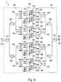
- Fig. 6 shows a filter arrangement 1 not part of the claimed invention for filtering a transmit signal received at a filter arrangement input 102 and providing a filtered transmit signal at a filter arrangement output 103.
- the filter arrangement of Fig. 6 is similar to the filter arrangement 1 described in Fig. 3 and comprises also a divide stage 200 and a combine stage 400.
- the divide stage 200 and the combine stage 400 are identical to the divide stage 200 and the combine stage 400 shown in Fig. 3 .
- this aspect of the present disclosure uses as filter elements a first duplex filter 510, a second duplex filter 520, a third duplex filter 530, a fourth duplex filter 540, a fifth duplex filter 550, a sixth duplex filter 560, a seventh duplex filter 570, and an eighth duplex filter 580.
- a first divider stage output 201 of the divider stage 200 is connected to a first duplex filter transmit port 511 of the first duplex-filter 510; a second divider stage output 202 of the divider stage 200 is connected to a second duplex filter transmit port 521, a third divider stage output 203 of the divider stage 200 is connected to a third duplex filter transmit port 531, a fourth divider stage output 204 of the divider stage 200 is connected to a fourth duplex filter transmit port 541, a fifth divider stage output 205 of the divider stage 200 is connected to a fifth duplex filter transmit port 551, a sixth divider stage output 206 of the divider stage 200 is connected to a sixth duplex filter transmit port 561, a seventh divider stage output 207 of the divider stage 200 is connected to a seventh duplex filter transmit port 571, and an eighth divider stage output 208 of the divider stage 200 is connected to a eighth duplex filter transmit port 581.
- a first duplex filter antenna port 513 is connected to a first combine stage input 401 of the combine stage 400; a second duplex filter antenna port 523 is connected to a second combine stage input 402 of the combine stage 400; a third duplex filter antenna port 533 is connected to a third combine stage input 403 of the combine stage 400; a fourth duplex filter antenna port 543 is connected to a fourth combine stage input 404 of the combine stage 400; a fifth duplex filter antenna port 553 is connected to a fifth combine stage input 405 of the combine stage 400; a sixth duplex filter antenna port 563 is connected to a sixth combine stage input 406 of the combine stage 400; a seventh duplex filter antenna port 573 is connected to a seventh combine stage input 407 of the combine stage 400; and a eighth duplex filter antenna port 583 is connected to a eighth combine stage input 408 of the combine stage 400.
- a first duplex filter receive port 512 is loaded with a first load impedance 514; a second duplex filter receive port 522 is loaded with a second load impedance 524; a third duplex filter receive port 532 is loaded with a third load impedance 534; a fourth duplex filter receive port 542 is loaded with a fourth load impedance 544, a fifth duplex filter receive port 552 is loaded with a fifth load impedance 554, a sixth duplex filter receive port 562 is loaded with a sixth load impedance 564; a seventh duplex filter receive port 572 is loaded with a seventh load impedance 574; and an eighth duplex filter receive port 582 is loaded with an eighth load impedance 584.
- the combine stage combines the eight filtered transmit signal portions into a single signal, which is provided at the combine stage output 409 of the combine stage 400. Due to the eight parallel duplex filters, the power durability of the filter arrangement can be increased to the eight times of the power durability of a single duplex filter.
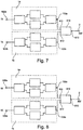
- a first filter arrangement 1a and a second filter arrangement 1b may be used in a multi-band transmitter for transmitting signals in two different frequency bands but profiting from the two different frequency bands sharing the same antenna.
- a first filter arrangement output 103a of the first filter arrangement 1a is connected to a first antenna coupler port 611 of an antenna coupler 610 and a second filter arrangement output 103b of the second filter arrangement 1b is connected to a second antenna coupler port 612 of the antenna coupler 610.
- a third antenna coupler port 613 provides the combined output signal of a first transmit signal TX.
- the antenna coupler 610 is a bidirectional coupler and should be a duplexer to avoid losses in the signals.
- a first filter arrangement input 102a is connected to a first antenna coupler port 611 and a second filter arrangement input 102b is connected to a second antenna coupler port 612.
- the antenna coupler 610 distributes a receive signal RX to the first antenna coupler port 611 and the second antenna coupler port 612.
- the filter elements in the first filter arrangement 1a are adapted for filtering signal in a first receive frequency band and the filter elements in the second filter arrangement 1b are adapted to filter signals in a second receive frequency band. As the first receive frequency band and the second receive frequency band are distinct from each other, an input signal passes either the first filter arrangement 1a or the filter arrangement 1b.
- a signal outside of the first receive frequency band and outside of the second frequency band will be blocked from the first filter arrangement 1a as well as from the second filter arrangement 1b.
- the first filter arrangement 1a and the second filter arrangement 1b may be used in a multi-band receiver to receive signals in two different receive frequency bands and process them separately.
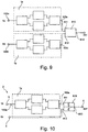
- Fig. 9 shows another aspect of the present disclosure not part of the claimed invention with a first filter arrangement 1a that is used in the transmitter of a transceiver and a second filter arrangement 1b that is used in the receiver of a transceiver.
- a first filter arrangement output 103a of the first filter arrangement 1a is connected to a first antenna coupler port 611 of the antenna coupler 610.
- a second filter arrangement input 102b is connected to a second antenna coupler port 612 of the antenna coupler 610.
- a third antenna coupler port 613 is connected to an antenna terminal as mentioned in connection with Fig. 7 .
- the coupler 610 should preferably be a duplexer to avoid substantially signal losses.
- the antenna coupler 610 is formed by a bidirectional antenna coupler which passes the filtered transmit signal from the first antenna coupler port 611 to the third antenna coupler port 613 and a receive signal, received a the third antenna port 613, to the second antenna coupler port 612.
- the antenna duplex filter 610 substantially passes a receive signal RX from the antenna terminal to the second filter arrangement 1b and substantially passes a transmit signal from a first filter arrangement input 102a and the antenna duplex filter 610 to the antenna terminal.
- the first filter arrangement 1a and the second filter arrangement 1b can be any of the described first filter arrangements in Fig. 1, Fig. 2 , Fig. 3 , Fig. 4, Fig. 5 , or Fig. 6 but are not limited to the described filter arrangements in the present disclosure.
- the first filter arrangement 1a and the second filter arrangement 1b have an identical structure, but not necessarily adapted to the same frequencies, such a filter arrangement may be called symmetrical.
- the first filter arrangement 1a may differ from the second filter arrangement 1b in the number of signal dividers, filter elements and signal combiners. In the following aspects of the present disclosure, some of the various combinations of such an asymmetrical filter design are described and discussed.
- Fig. 10 shows another aspect of the present disclosure not part of the claimed invention with a transmit filter arrangement 1a that is connected to a first antenna duplex filter transmit port 611 of a first antenna duplex filter 610 thus providing a duplex filter arrangement 2.
- the first antenna duplex filter 610 is used in this aspect of the present disclosure to separate transmit signals TX provided at a duplex filter arrangement antenna port 613 and receive signals RX received at the duplex filter arrangement antenna port 613.
- the transmit signal TX is passed to the first filter arrangement input 102a of the first transmit filter arrangement 1a.
- the first filter arrangement 1a can be any of the described first filter arrangements in Fig. 1, Fig. 2 , Fig. 3 , Fig. 4, Fig. 5 , or Fig. 6 but is not limited to the described filter arrangements in the present disclosure.
- the first filter arrangement output 103a of the first filter arrangement 1a is connected to the first antenna duplex filter transmit port 611 of the first antenna duplex filter 610.
- a first antenna duplex filter antenna port 613 of the first antenna duplex filter 610 forms an antenna terminal 5 for providing an antenna signal ANT.
- a first antenna duplex filter receive port 612 of the first antenna duplex filter 610 passes signals received at the antenna port 5, which are in the receive band, to a duplex filter arrangement receiver terminal 4.
- This duplex filter arrangement 2 may be termed asymmetric, as the number of filter elements that the transmit signal TX passes from the duplex filter arrangement transmit terminal 3 to the antenna terminal 5 (transmit path) differs from the number of filter elements the receive signal RX passes from the antenna terminal 5 to the duplex filter receiver terminal 4 (receive path).
- the number of filter elements in line in the transmit path is two and in the receive path is one.
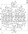
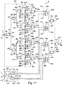
- FIG. 11 Another aspect of the present disclosure and which is part of the claimed invention is shown in Fig. 11 . It is another asymmetric duplex filter arrangement 2 for filtering a transmit signal TX, received at a duplex filter arrangement transmit port 3 and providing the filtered transmit signal at a duplex filter arrangement antenna port 5.
- a receive signal RX, received at the duplex filter arrangement antenna port 5 is filtered and provided at a duplex filter arrangement receive port 4.
- some duplex filter elements are merged in a structure of bidirectional couplers.
- the duplex filter arrangement 2 of this aspect of the present disclosure is now described in more detail.
- At least the first signal combiner 410 is a bidirectional coupler, such as a so-called Wilkinson combiner or a so-called quadrature hybrid.
- the advantage of a bidirectional coupler in this duplex filter arrangement is, that the first signal combiner works for the partial transmit signals passed on to the first combiner input 411 and the second signal combiner input 412 as a signal combiner and for a receive signal as a signal divider at the same time.
- a Wilkinson combiner has the advantage over the quadrature combiner in that the outputs of the Wilkinson combiner are in phase with each other, whereas the outputs of the quadrature combiner have a 90° phase difference. This means that in using the quadrature combiner a circuit designer needs to take care in ensuring that the signals to be continued are in phase with each other.
- the transmit signal TX is passed from the duplex-filter arrangement transmit port 3 to a transmit divide stage input 209.
- the transmit divide stage 200 is formed by a first transmit divider 210, a second transmit divider 220, a third transmit divider 230, a fourth transmit divider 240, a fifth transmit divider 250, a sixth transmit divider 260 and a seventh transmit divider 270.
- a first transmit signal combiner input 211 is identical to the transmit combine stage input 209.
- the first transmit divider 210 splits the transmit signal TX, received at the first transmit divider input 210 into a first portion and a second portion of the transmit signal.
- the first portion of the transmit signal TX is provided at a first transmit divider output 212 and the second portion of the transmit signal TX is provided at a second transmit divider output 213.
- the first transmit divider output 212 is connected to a second transmit divider input 221 of the second transmit divider 220 and the second transmit divider output 213 is connected to a third transmit divider input 231 of the third transmit divider 230.
- the second transmit divider 220 splits a second transmit divider input signal, received at the second transmit divider input 221 into a third portion and a fourth portion of the second transmit divider input signal.
- the third portion of the second transmit divider input signal is provided at a third transmit divider output 222.
- the fourth portion of the second transmit divider input signal is provided at a fourth transmit divider output 223.
- the third transmit divider output 222 is connected to a fourth transmit divider input 241 of the fourth transmit signal combiner 240.
- a seventh transmit divider output 242 and an eighth transmit divider output 243 of the fourth transmit signal combiner 240 finally form the first transmit divide stage output 201 and the second transmit divide stage output 202.
- the fourth transmit divider output 223 is connected to a fifth transmit divider input 251 of the fifth transmit divider 250
- the fifth transmit divider output 232 is connected to a sixth transmit divider input 261 of the sixth transmit divider 260
- the sixth transmit divider output 233 is connected to a seventh transmit divider input 271 of the seventh transmit divider 270.
- a seventh transmit divider output 241 of the fourth transmit divider 240 forms the first transmit divide stage output 201 of the transmit divide stage 200; an eighth transmit divider output 242 of the fourth transmit divider 240 forms the second transmit divide stage output 202 of the transmit divide stage 200; a ninth transmit divider output 252 of the fifth transmit divider 250 forms the third transmit divide stage output 203 of the transmit divide stage 200; a tenth transmit divider output 253 of the fifth transmit divider 250 forms the fourth transmit divide stage output 204 of the transmit divide stage 200; a eleventh transmit divider output 262 of the sixth transmit divider 260 forms the fifth transmit divide stage output 205 of the transmit divide stage 200; a twelfth transmit divider output 263 of the sixth transmit divider 260 forms the sixth transmit divide stage output 206 of the transmit divide stage 200; a thirteenth transmit divider output 272 of the seventh transmit divider 270 forms the seventh transmit divide stage output 207 of the transmit divide stage 200; and a fourteenth transmit divider output 273 of the seventh transmit divider 270
- the power of the transmit filter arrangement input signal 101 is equally split into eight separate signal portions which are passed in parallel through a first duplex filter element 510, a second duplex filter element 520, a third duplex filter element 530, a fourth duplex filter element 540, a fifth duplex filter element 550, a sixth duplex filter element 560, a seventh duplex filter element 570, and an eighth duplex filter element 580 of the transmit filter stage 500.
- the eight duplex filter elements 510 ... 580 are wired in the same manner as in the aspect of the present disclosure shown in Fig. 6 .
- a transmit combine stage 400 in this aspect of the present disclosure is extended to eight signal combiner input signals.
- a first transmit combine stage input 401 is connected to a seventh transmit combiner input 441 of a fourth transmit combiner 440; a second combine stage input 402 is connected to an eighth transmit combiner input 442 of the fourth transmit combiner 440; a third combine stage input 403 is connected to a ninth transmit combiner input 451 of a fifth transmit combiner 450; a fourth combine stage input 404 is connected to a tenth transmit combiner input 452 of the fifth transmit combiner 450; a fifth combine stage input 405 is connected to an eleventh transmit combiner input 461 of a sixth transmit combiner 460; a sixth combine stage input 406 is connected to a twelfth transmit combiner input 462 of the sixth transmit combiner 460; a seventh combine stage input 407 is connected to a thirteenth transmit combiner input 471 of a seventh transmit combiner 470; a eighth combine stage input
- the transmit combiners that form the transmit combiner stage and duplex filters for branching out of a receive signal are mixed.
- duplex-filter elements used for branching out the receive signal are termed antenna duplex-filter.
- a fourth transmit combiner output 443 of the fourth transmit combiner 440 is connected to a first transmit port 611 of a first antenna duplex filter 610.
- a fifth transmit combiner output 453 of the fifth transmit combiner 450 is connected to a second transmit port 621 of a second antenna duplex filter 620.
- a sixth transmit combiner output 463 of the sixth transmit combiner 460 is connected to a third transmit port 631 of a third antenna duplex filter 630; and a seventh transmit combiner output 473 of the seventh transmit combiner 470 is connected to a fourth transmit port 641 of a fourth antenna duplex filter 640.
- a first antenna port 613 of the first antenna duplex filter 610 is connected to a third transmit combiner input 421 of a second transmit combiner 420 and a second antenna port 623 of the second transmit combiner 620 is connected to a fourth transmit combiner input 422 of the second transmit combiner 420.
- a third antenna port 633 of the third antenna duplex filter 630 is connected to a fifth transmit combiner input 431 of the third transmit combiner 430 and a fourth antenna port 643 of the fourth antenna duplex filter 640 is connected to a sixth transmit combiner input 432 of the third transmit combiner 430.
- a second transmit combiner output 423 of the second transmit combiner 420 is connected to a first transmit combiner input 411 of the first transmit combiner 410; and a third transmit combiner output 433 of the third transmit combiner 430 is connected to a second transmit combiner input 412 of the first transmit combiner 410.
- the first transmit combiner output 413 of the first transmit combiner 410 forms the antenna terminal 5 of the duplex filter arrangement 2.
- a first receive port 612 of the first antenna duplex filter 610 is connected to a third receive signal combiner input 721 of a second receive signal combiner 720.
- a second receive port 622 of the second antenna duplex filter 620 is connected to a fourth receive signal combiner input 722 of a second receive signal combiner 720.
- a third receive port 632 of the third antenna duplex filter 630 is connected to a fifth receive signal combiner input 731 of a third receive signal combiner 730.
- a fourth receive port 642 of the fourth antenna duplex filter 640 is connected to a sixth receive signal combiner input 732 of the third receive signal combiner 730.
- a second antenna signal combiner output 723 of the second antenna signal combiner 720 is connected to a first receive signal combiner input 711 of a first receive signal combiner 710.
- a third antenna signal combiner output 733 of the third antenna signal combiner 730 is connected to a second receive signal combiner input 712 of the first signal combiner 710.
- the first receive signal combiner output 713 provides a receive signal RX at a receiver terminal 4 for example for a following receiver.
- the first transceiver combiner 410, the second transceiver combiner 420 and the third transceiver combiner 430 are in this aspect of the present disclosure chosen as bidirectional couplers.
- a bidirectional coupler such as a quadrature hybrid, or a Wilkinson coupler combine signals received at a first port and a second port into a single signal provided at a third port and in an inverse manner a signal received at the third port is split into two equal signal portions provided at the first port and the second port of the bidirectional coupler. Due to the way the filter arrangements are wired, all of the signal dividers and all of the signal combiners may be chosen as bidirectional couplers without changing the function of the described filter arrangements or deteriorating the signals. The advantage of choosing all signal dividers and all signal combiners as bidirectional couplers is that less different types of circuit elements are used in the filter arrangement which helps to simplify the manufacturing process.
- Wilkinson splitters/combiners and quadrature couplers can be used mixed with the restriction that in one level of splitting/combining only the identical type is used, e..g. in Figure 2 : the first signal divider 210 and the first signal combiner 410 could be quadrature and the second signal divider 220, the third signal divider 230, the second signal combiner 420 and the third signal combiner 430 could be Wilkinson.
- first signal divider 210 and the first signal combiner 410 could be Wilkinson and whereas the second signal divider 220, the third signal divider 230, the second signal combiner 420 and the third signal combiner 430 can be quadrature. It will be appreciated that a combination of different elements comprising Wilkinson splitters/combiners and quadrature couplers can be used, but it is necessary to ensure that the choice of the elements is such that the phases of the combined signal are correct.
- the receive signal When passing from the antenna terminal 5 through the first transmit combiner 410 the receive signal is split due to the bidirectional character of the first transmit combiner 410 into a first receive signal portion provided at the first transmit combiner input 411 and a second receive signal portion provided at the second transmit combiner input 412.
- the third receive portion signal passes the first antenna duplex filter 610 from the first antenna port 613 to the first receive port 612 of the first antenna duplex-filter 610 and the fourth receive portion signal passes the second antenna duplex filter 620 from the second antenna port 623 to the second receive port 622 of the second antenna duplex-filter 620.
- the second receive portion signal is further split in the third transmit combiner 430 into a fifth receive portion signal, provided at the fifth transmit combiner input 431 and a sixth receive portion signal provided at the sixth transmit combiner input 432.
- the fifth receive portion signal passes the third antenna duplex filter 630 from the third antenna port 633 to the third receive port 632 of the third antenna duplex-filter 630.
- the sixth receive portion signal passes the fourth antenna duplex filter 640 from the fourth antenna port 643 to the fourth receive port 642 of the fourth antenna duplex-filter 640
- the receive signal portion RX all signals outside the receive band, that are present at the antenna terminal 5, are adequately suppressed when the receive signal portions pass in parallel the first antenna duplex filter 610 from the first antenna port 613 to the first receiver port 612, the second antenna duplex filter 620 from the second antenna port 623 to the second receiver port 622, the third antenna duplex filter 630 from the third antenna port 633 to the third receiver port 632 and the fourth antenna duplex filter 640 from the fourth antenna port 643 to the fourth receiver port 642.
- the filtered fraction signals are recombined in the receive combine stage 700.
- duplex filter arrangement With this duplex filter arrangement, a fourfold higher power can be passed from the transmit terminal 3 to the antenna terminal 5.
- two duplex filter elements are always in each possible transmit path for a signal passing from the transmit terminal 3 to the antenna terminal 4 the out of band signals in the transmit signals are filtered twice one after each other and therefore are better suppressed.
- each portion of the receive signal, passing from the antenna terminal 5 to the receiver terminal 4 is subjected only once to filtering which keeps the insertion loss low and thus enables a better receiver sensitivity.
- the power capability of the filter arrangements of this disclosure is limited by the filter stage with the lower number of parallel components.
- the first filter stage either four or eight filters could be used.
- the use of eight filters enables the use of eight different lower power amplifiers after the splitter network.
- the present disclosure further relates to a computer program product embedded on a computer readable medium.
- the computer program product comprises executable instructions for the manufacture of the filter arrangement of the present disclosure.
- implementations may also be embodied in software (e.g., computer readable code, program code, and/or instructions disposed in any form, such as source, object or machine language) disposed, for example, in a computer usable (e.g., readable) medium configured to store the software.
- software e.g., computer readable code, program code, and/or instructions disposed in any form, such as source, object or machine language
- a computer usable (e.g., readable) medium configured to store the software.
- Such software can enable, for example, the function, fabrication, modeling, simulation, description and/or testing of the apparatus and methods described herein.
- this can be accomplished through the use of general programming languages (e.g., C, C++), hardware description languages (HDL) including Verilog HDL, VHDL, a layout description language (GDS, GDS II, Gerber, ...), a circuit description language (Spice) and so on, or other available programs.
- HDL hardware description languages
- Such software can be disposed in any known computer usable medium such as semiconductor, magnetic disk, or optical disc (e.g., CD-ROM, DVD-ROM, etc.).
- the software can also be disposed as a computer data signal embodied in a computer usable (e.g., readable) transmission medium (e.g., carrier wave or any other medium including digital, optical, or analogue-based medium).
- Embodiments of the present invention may include methods of providing the apparatus described herein by providing software describing the apparatus and subsequently transmitting the software as a computer data signal over a communication network including the Internet and intranets. It is understood that the apparatus and method described herein may be included in a semiconductor intellectual property core, such as a microprocessor core (e.g., embodied in HDL) and transformed to hardware in the production of integrated circuits. Additionally, the apparatus and methods described herein may be embodied as a combination of hardware and software. Thus, the present invention should not be limited by any of the above-described exemplary embodiments, but should be defined only in accordance with the following claims.
Landscapes
- Physics & Mathematics (AREA)
- Acoustics & Sound (AREA)
- Surface Acoustic Wave Elements And Circuit Networks Thereof (AREA)
- Transceivers (AREA)
Claims (17)
- Eine Duplex-Filteranordnung (2) für die Filterung eines Funksignals, die Duplex-Filteranordnung (2) umfassend einen Sende-Port (3), einen Empfangs-Port (4) und einen Antennen-Port (5) und ferner umfassend:mindestens eine Sende-Filteranordnung zur Weiterleitung der an dem Sende-Port (3) empfangenen Signale an den Antennen-Port (5), die mindestens eine Sende-Filteranordnung umfassend mindestens ein erstes und ein zweites Duplex-Filterelement, wobei das erste Duplex-Filterelement und das zweite Duplex-Filterelement jeweils umfassen:eine Teilungsstufe (240, 250) zur Zerlegung des Duplex-Filterelements in mindestens einen ersten Signalabschnitt und mindestens einem zweiten Signalabschnitt, wobei der mindestens eine erste Signalabschnitt weitergeleitet wird an einen Ausgang einer mindestens ersten Teilungsstufe und der mindestens eine zweite Signalabschnitt weitergeleitet wird an einen mindestens zweiten Ausgang der Teilungsstufe;mindestens ein erstes Filterelement (510; 530) umfassend einen Eingang des ersten Filterelements verbunden mit dem ersten Ausgang der Teilungsstufe, und einen Ausgang des ersten Filterelements, um mindestens ein erstes gefiltertes Signals bereitzustellen;mindestens ein zweites Filterelement (520; 540) umfassend einen Eingang des zweiten Filterelements verbunden mit dem zweiten Ausgang der Teilungsstufe, und einen Ausgang des zweiten Filterelements, um mindestens ein zweites gefiltertes Signal bereitzustellen,eine Kombinations-Stufe (400) für die Kombination des ersten gefilterten Signals, aufgenommen am ersten Eingang der Kombinations-Stufe, und des zweiten gefilterten Signals, aufgenommen am zweiten Eingang der Kombinations-Stufe, zu einem Duplex-Filterelement-Ausgangssignal,- wobei die Filteranordnung ferner einen ersten und zweiten Antennen-Duplex-Filter (610, 620) umfasst- der erste Antennen-Duplex-Filter (610) und der zweite Antennen-Duplex-Filter (620) jeweils erste, zweite und dritte Ports (611, 612, 613; 621, 622, 623) aufweisend und ein gefiltertes Sendesignal von dem ersten Port (611) an den dritten Port (613) weiterleitend, und das am dritten Port (613) empfangene Empfangssignal an den zweiten Port (612) weiterleitend- der erste Antennen-Duplex-Filter und der zweite Antennen-Duplex-Filter (610, 620) am ersten Port verbunden mit einem korrespondierenden ersten und zweiten Duplex-Filterelement, die an dem Antennen-Port (5) empfangenen Signale an den Empfangs-Port (4) weiterleitend.
- Die Duplex- Filteranordnung nach Anspruch 1, umfassend einen ersten Signalteiler (210) und mindestens einen zweiten Signalteiler (220) zur Aufteilung des Eingangssignals der Duplex-Filteranordnung, wobei mindestens ein erster Signalteiler-Ausgang des ersten Signalteilers mit mindestens einem ersten Signalteiler-Eingang des zweiten Signalteilers verbunden ist.
- Die Duplex-Anordnung nach Anspruch 1 oder 2, umfassend zur Bereitstellung des Ausgangssignals des Duplex-Filterelements, mindestens einen ersten Signalkombinierer (410) und einen zweiten Signalkombinierer (420), wobei ein Ausgang des ersten Signalkombinierers mit mindestens einem Eingang des zweiten Signalkombinierers verbunden ist.
- Die Duplex-Filteranordnung nach einem der vorhergehenden Ansprüche, wobei mindestens eines aus dem ersten Duplex-Filterelement (510, 530) oder dem zweiten Duplex-Filterelement (520, 540) ein Duplex-Filter ist, mit einem ersten Sende-Port zur Weiterleitung eines Signals in einem ersten Frequenzband an einen ersten Antennen-Port des Duplex-Filters, und einen ersten Empfangs-Port für den Empfang eines zweiten Signals in einem zweiten Frequenzband von dem ersten Antennen-Port, wobei einer aus dem ersten Empfangs-Port des Duplex-Filters oder dem Sende-Port des Duplex-Filters über eine Impedanz mit einer Referenzebene verbunden ist.
- Die Duplex-Filteranordnung nach einem der vorhergehenden Ansprüche, wobei mindestens eines aus dem ersten Duplex-Filterlement (510; 530) oder dem zweiten Duplex-Filterlement (520;540) ein Film-Bulk-Acoustic-Resonator-Filter (FBAR) ist.
- Die Duplex-Filteranordnung nach Anspruch 5, wobei der Film-Bulk-Acoustic-Resonator-Filter (FBAR) ein Duplex-Filter ist, mit einem ersten Port zur Weiterleitung eines Signals in einem ersten Frequenzband an einen Antennen-Port, wobei einer aus dem ersten Port des FBAR-Duplexers oder dem zweiten Port des FBAR-Filters über eine Impedanz mit einer Referenzebene verbunden ist.
- Die Duplex-Filteranordnung nach Anspruch 2 oder einem der Ansprüche 3 bis 6 sofern abhängig von Anspruch 2, wobei der erste Signalteiler (240; 250) und der erste Signalkombinierer (440, 450) bidirektionale Koppler sind.
- Die Duplex-Filteranordnung nach Anspruch 7, wobei mindestens einer der bidirektionalen Koppler ein Wilkinson-Kombinierer oder ein Quadratur-Hybrid ist.
- Die Duplex-Filteranordnung nach einem der vorhergehenden Ansprüche, wobei mindestens eine Sende-Filteranordnung für die Filterung eines der Sendesignale oder der Empfangssignale eingerichtet ist.
- Die Duplex-Filteranordnung nach einem der vorstehenden Ansprüche, wobei
mindestens eine erste Sende-Filteranordnung mit mindestens einer zweiten Filteranordnung verbunden ist, übernommen für die Filterung eines der Sendesignale oder der Empfangssignale; und ferner umfassend einen Antennenkoppler zum Verbinden von mindestens der ersten Sende-Filteranordnung und mindestens der zweiten Filteranordnung, eine oder
mehrere der folgenden Funktionen bereitstellend:- Filterung eines ersten Empfangssignals in mindestens der ersten Sende-Filteranordnung und Filterung eines zweiten Empfangssignals in mindestens der zweiten Filteranordnung- Filterung eines ersten Sendesignal in mindestens der ersten Sende-Filteranordnung und Filterung eines ersten Empfangssignals in mindestens der zweiten Filteranordnung,- Filterung eines ersten Sendesignals in mindestens der ersten Sende-Filteranordnung und Filterung eines zweiten Sendesignals in mindestens der zweiten Filteranordnung. - Die Duplex-Filteranordnung nach Anspruch 10, wobei sich die Anzahl der Filterelemente (510, 520, 530, 540, 550, 560, 570, 580) in der ersten Sende-Filteranordnung von der Anzahl der Filterelemente in der zweiten Filteranordnung unterscheidet.
- Der Duplex-Filteranordnung nach Anspruch 10 oder 11, wobei- die erste Sende-Filteranordnung für die Filterung eines Sendesignals eingerichtet ist und die Anzahl der Filterelemente (510, 520, 530, 540, 550, 560, 570, 580) in der ersten Sende-Filteranordnung acht beträgt; und- die zweite Filteranordnung für die Filterung eines Empfangssignals eingerichtet ist und die Anzahl der Filterelemente in der zweiten Filteranordnung vier beträgt.
- Der Duplex-Filteranordnung nach einem der Ansprüche 10 bis 12, wobei- ein erstes Signal aufgeteilt wird durch einen ersten Signalteiler in einem ersten Signalabschnitt an einem ersten Signalteiler-Ausgang, einen zweiten Signalabschnitt an einem zweiten Signalteiler-Ausgang, einen dritten Signalabschnitt an einem dritten Signalteiler-Ausgang, einen vierten Signalabschnitt an einem vierten Signalteiler-Ausgang, einen fünften Signalabschnitt an einem fünften Signalteiler-Ausgang, einen sechsten Signalabschnitt an einem sechsten Signalteiler-Ausgang, einen siebenten Signalabschnitt an einem siebenten Signalteiler-Ausgang, und einen achten Signalabschnitt an einem achten Signalteiler-Ausgang,die Duplex-Filteranordnung ferner umfassend:- ein erstes Sende-Filterelement (510) verbunden mit einem ersten Sende-Filterelement-Eingang an den ersten Ausgang der Sende-Filteranordnung und ein erstes TX-gefiltertes Signal an einem ersten Sende-Filter-Ausgang bereitstellend;- ein zweites Sende-Filterelement (520) verbunden mit einem zweiten Sende-Filter-Eingang an den zweiten Ausgang der Teilungsstufe und ein zweites TX gefiltertes Signal an einem zweiten Sende-Filter-Ausgang bereitstellend;- ein drittes Sende-Filterelement (530) verbunden mit einem dritten Sende-Filter-Eingang an den dritten Ausgang der Teilungsstufe und ein drittes TX gefiltertes Signal an einem dritten Sende-Filter-Ausgang bereitstellend;- ein viertes Sende-Filterelement (540) verbunden mit einem vierten Sende-Filter-Eingang an den vierten Ausgang der Teilungsstufe und ein viertes TX gefiltertes Signal an einem vierten Sende-Filter-Ausgang bereitstellend;- ein fünftes Sende-Filterelement (550) verbunden mit einem fünften Sende-Filter-Eingang an den fünften Ausgang der fünften Teilungsstufe und ein fünftes TX gefiltertes Signal an einem fünften Sende-Filter-Ausgang bereitstellend;- ein sechstes Sende-Filterelement (560) verbunden mit einem sechsten Sende-Filter-Eingang an den sechsten Ausgang der Teilungsstufe und ein sechstes TX gefiltertes Signal an einem sechsten Sende-Filter-Ausgang bereitstellend;- ein siebtes Sende-Filterelement (570) verbunden mit einem siebten Sende-Filter-Eingang an den siebten Ausgang der Teilungsstufe und ein siebtes TX gefiltertes Signal an einem siebten Sende-Filter-Ausgang bereitstellend;- ein achtes Sende-Filterelement (580) verbunden mit einem achten Sende-Filter-Eingang an den achten Ausgang der Teilungsstufe und ein achtes TX gefiltertes Signal an einem achten Sende-Filter-Ausgang bereitstellend;- ein erster Signalkombinierer (210) zum Kombinieren des ersten gefilterten TX-Signal und des zweiten gefilterten TX-Signal, ein erstes kombiniertes TX-Signal an einem Ausgang des ersten Signalkombinierers bereitstellend;- ein zweiter Signalkombinierer (220) zum Kombinieren des dritten gefilterten TX-Signal und des vierten gefilterten TX-Signal, ein zweites kombiniertes TX-Signal an einem Ausgang des zweiten Signalkombinierers bereitstellend;- ein dritter Signalkombinierer (230) zum Kombinieren des fünften gefilterten TX-Signal und des sechsten gefilterten TX-Signal, ein drittes kombiniertes TX-Signal an einem Ausgang des dritten Signalkombinierers bereitstellend;- ein vierter Signalkombinierer (240) zum Kombinieren des siebten gefilterten TX-Signal und des achten gefilterten TX-Signal, ein viertes kombiniertes TX-Signal an einem Ausgang des vierten Signalkombinierers bereitstellend;- ein erster Duplex-Filter (610) umfassend einem ersten Sende-Port verbunden mit dem ersten Signalkombinierer-Ausgang, und ferner umfassend einen ersten Antennen-Port verbunden mit einem neunten Signalkombinierer-Eingang eines fünften Signalkombinierers;- ein zweiter Duplex-Filter (620) umfassend einen zweiten Sende-Port verbunden mit dem zweiten Signalkombinierer-Ausgang, und ferner umfassend eine zweiter Antennen-Port verbunden mit einem zehnten Signalkombinierer-Eingang eines fünften Signalkombinierers;- ein dritter Duplex-Filter (630) umfassend einen dritten Sende-Port verbunden mit dem dritten Signalkombinierer-Ausgang, und ferner umfassend einen dritten Antennen-Port verbunden mit einem elften Signalkombinierer-Eingang eines sechsten Signalkombinierers;- ein vierter Duplex-Filter (640) umfassend einen vierten Sende-Port verbunden mit der vierten Signalkombinierer-Ausgang, und ferner umfassend einen vierten Antennen-Port, verbunden mit einem zwölften Signalkombinierer-Ausgang eines sechsten Signalkombinierers;- ein erster bidirektionaler Koppler umfassend einen ersten Koppler-Port verbunden mit dem ersten Antennen-Port des ersten Duplex-Filters, und ferner umfassend einen zweiten Koppler-Port verbunden mit dem zweiten Antennen-Port des zweiten Duplex-Filters, und ferner umfassend einen dritten Koppler-Port;- eine zweiter bidirektionaler Koppler umfassend einen vierten Koppler-Port verbunden mit dem dritten Antennen-Port des dritten Duplex-Filters, ferner umfassend einen fünften Koppler-Port verbunden mit dem vierten Antennen-Port des vierten Duplex-Filters, und ferner umfassend einen sechsten Koppler-Port;- ein dritter bidirektionalen Koppler, umfassend einen siebten Koppler-Port, verbunden mit dem dritten Koppler-Port des ersten bidirektionalen Kopplers, und ferner umfassend einen achten Koppler-Port, der mit dem sechsten Koppler-Port des zweiten bidirektionalen Kopplers verbunden ist, und ferner umfassend einen neunten Koppler-Port für die Bereitstellung eines Sende-Filter-Ausgangssignals für eine Antenne und für den Empfang eines Empfangssignal von der Antenne;- ein Kombinations-Stufe umfassend einen ersten Eingang der Kombinations-Stufe verbunden mit einem ersten Empfangs-Port des ersten Duplex-Filters für den Empfang eines ersten Empfangs-Signalabschnitts, ein zweiter Eingang der Kombinations-Stufe verbunden mit einer zweiten Empfangs-Port des zweiten Duplex-Filters für den Empfang eines zweiten Empfangs-Signalabschnitts, ein dritter Eingang der Kombinations-Stufe verbunden mit einem dritten Empfangs-Port des dritten Duplex-Filters für den Empfang eines dritten Empfangs-Signalabschnitts, und ein vierter Eingang der Kombinations-Stufe verbunden mit einem vierten Empfangs-Port des vierten Duplex-Filters für den Empfang eines vierten Empfangs-Signalabschnitts, weiter umfassend einen Ausgang der Kombinations-Stufe für Bereitstellung eines kombinierten Empfangssignals des ersten Empfangs-Signalabschnitts, des zweiten Empfangs-Signalabschnitts, des dritten Empfangs-Signalabschnitts, und des vierten Empfangs-Signalabschnitts.
- Ein Chipsatz umfassend eine Duplex-Filteranordnung (2) nach Anspruch 1.
- Eine Funkstation, umfassend eine Duplex-Filteranordnung (2) nach Anspruch 1.
- Ein Verfahren zur Herstellung einer Duplex-Filteranordnung (2) nach Anspruch 1.
- Ein Computerprogrammprodukt, umfassend ein nicht vergängliches Computernutzbares Medium mit einer darin gespeicherten Steuerlogik, um einen Computer zu veranlassen, eine Duplex-Filteranordnung (2) nach Anspruch 1 herzustellen.
Applications Claiming Priority (2)
| Application Number | Priority Date | Filing Date | Title |
|---|---|---|---|
| US13/253,256 US8600330B2 (en) | 2011-10-05 | 2011-10-05 | Filter arrangement |
| PCT/EP2012/067301 WO2013050209A1 (en) | 2011-10-05 | 2012-09-05 | Filter arrangement |
Publications (2)
| Publication Number | Publication Date |
|---|---|
| EP2764618A1 EP2764618A1 (de) | 2014-08-13 |
| EP2764618B1 true EP2764618B1 (de) | 2017-05-31 |
Family
ID=46832375
Family Applications (1)
| Application Number | Title | Priority Date | Filing Date |
|---|---|---|---|
| EP12758447.2A Not-in-force EP2764618B1 (de) | 2011-10-05 | 2012-09-05 | Filteranordnung |
Country Status (6)
| Country | Link |
|---|---|
| US (1) | US8600330B2 (de) |
| EP (1) | EP2764618B1 (de) |
| KR (1) | KR101722938B1 (de) |
| CN (1) | CN103918180B (de) |
| AU (1) | AU2012320818B2 (de) |
| WO (1) | WO2013050209A1 (de) |
Families Citing this family (22)
| Publication number | Priority date | Publication date | Assignee | Title |
|---|---|---|---|---|
| GB2496390B (en) * | 2011-11-08 | 2017-06-28 | Filtronic Wireless Ltd | A filter block and a signal transceiver comprising such a filter block |
| US9929850B2 (en) * | 2013-04-17 | 2018-03-27 | Snaptrack, Inc. | Circuit arrangement |
| US9570222B2 (en) * | 2013-05-28 | 2017-02-14 | Tdk Corporation | Vector inductor having multiple mutually coupled metalization layers providing high quality factor |
| US9935670B2 (en) | 2013-09-26 | 2018-04-03 | Qorvo Us, Inc. | Carrier aggregation using multiple antennas |
| US9985682B2 (en) * | 2013-10-24 | 2018-05-29 | Qorvo Us, Inc. | Broadband isolation low-loss ISM/MB-HB tunable diplexer |
| US9899986B2 (en) | 2013-10-24 | 2018-02-20 | Qoro US, Inc. | RF diplexer |
| US9735752B2 (en) | 2014-12-03 | 2017-08-15 | Tdk Corporation | Apparatus and methods for tunable filters |
| US9768880B2 (en) | 2015-05-20 | 2017-09-19 | Ciena Corporation | Method and system for nonlinear interference mitigation |
| EP3235129A1 (de) * | 2015-07-24 | 2017-10-25 | Huawei Technologies Co., Ltd. | Funkfrequenzduplexer |
| WO2017063689A1 (en) * | 2015-10-14 | 2017-04-20 | Telefonaktiebolaget Lm Ericsson (Publ) | A wireless communication node with multi-band filters |
| US10686424B2 (en) | 2015-11-12 | 2020-06-16 | Telefonaktiebolaget Lm Ericsson (Publ) | Duplexer |
| US9929769B1 (en) * | 2017-01-20 | 2018-03-27 | Resonant Inc. | Communications receiver using multi-band transmit blocking filters |
| US10547290B2 (en) | 2017-09-13 | 2020-01-28 | Apple Inc. | Multi-radio front-end circuitry for radio frequency imbalanced antenna sharing system |
| US11239985B2 (en) * | 2019-04-16 | 2022-02-01 | Cisco Technology, Inc. | Echo cancellation in multiple port full duplex (FDX) nodes and amplifiers |
| CN110971209B (zh) * | 2019-11-04 | 2023-10-20 | 天津大学 | 提高体声波滤波器功率容量的方法及滤波元件 |
| KR102895573B1 (ko) * | 2020-05-07 | 2025-12-05 | 삼성전자주식회사 | 무선 통신 시스템에서 안테나 필터 및 이를 포함하는 전자 장치 |
| US11368342B2 (en) * | 2020-09-09 | 2022-06-21 | Apple Inc. | Electrical phase balanced duplexer |
| US12107568B2 (en) | 2021-03-24 | 2024-10-01 | Murata Manufacturing Co., Ltd. | Composite transversely-excited film bulk acoustic resonator circuits having a capacitor for improved rejection |
| US12267063B2 (en) * | 2021-09-24 | 2025-04-01 | Rf360 Singapore Pte. Ltd. | Harmonic reduction with filtering |
| US12113511B2 (en) | 2022-03-16 | 2024-10-08 | Rf360 Singapore Pte. Ltd. | Bridge-type filters |
| US12231112B2 (en) | 2022-03-16 | 2025-02-18 | Rf360 Singapore Pte. Ltd. | Bridge-type filters |
| JP2024059391A (ja) * | 2022-10-18 | 2024-05-01 | Tdk株式会社 | 分波器 |
Citations (3)
| Publication number | Priority date | Publication date | Assignee | Title |
|---|---|---|---|---|
| US6567647B1 (en) * | 1998-03-26 | 2003-05-20 | Ericsson Inc. | Low noise radio frequency transceivers including circulators |
| US20090286569A1 (en) * | 2008-05-19 | 2009-11-19 | Nokia Corporation | Apparatus method and computer program for interference reduction |
| WO2013011026A2 (en) * | 2011-07-18 | 2013-01-24 | Ubidyne, Inc. | Amplifier arrangement |
Family Cites Families (9)
| Publication number | Priority date | Publication date | Assignee | Title |
|---|---|---|---|---|
| US5424680A (en) * | 1993-11-30 | 1995-06-13 | Harmonic Lightwaves, Inc. | Predistorter for high frequency optical communications devices |
| WO1995028746A2 (en) | 1994-04-14 | 1995-10-26 | E.I. Du Pont De Nemours And Company | High power high-temperature superconductive filters |
| US6522307B2 (en) | 2000-07-14 | 2003-02-18 | Lg Electronics Inc. | Antenna sharing apparatus of base station in W-CDMA system |
| US7230996B2 (en) * | 2002-06-13 | 2007-06-12 | Matsushita Electric Industrial Co., Ltd. | Transmitting circuit device and wireless communications device |
| JP3889351B2 (ja) * | 2002-12-11 | 2007-03-07 | Tdk株式会社 | デュプレクサ |
| TWI304700B (en) * | 2005-02-16 | 2008-12-21 | Wistron Neweb Corp | Wireless transmission device capable of transmitting media from multiple channels |
| US8314665B2 (en) | 2006-09-20 | 2012-11-20 | Trustees Of Boston University | Nano electromechanical integrated-circuit filter |
| KR20090036327A (ko) | 2007-10-09 | 2009-04-14 | 주식회사 이롬테크 | 고주파 필터 |
| CN102006029A (zh) | 2010-12-01 | 2011-04-06 | 浙江大学 | Fbar滤波器及其组件 |
-
2011
- 2011-10-05 US US13/253,256 patent/US8600330B2/en not_active Expired - Fee Related
-
2012
- 2012-09-05 KR KR1020147009533A patent/KR101722938B1/ko not_active Expired - Fee Related
- 2012-09-05 CN CN201280049279.1A patent/CN103918180B/zh not_active Expired - Fee Related
- 2012-09-05 EP EP12758447.2A patent/EP2764618B1/de not_active Not-in-force
- 2012-09-05 WO PCT/EP2012/067301 patent/WO2013050209A1/en not_active Ceased
- 2012-09-05 AU AU2012320818A patent/AU2012320818B2/en not_active Ceased
Patent Citations (3)
| Publication number | Priority date | Publication date | Assignee | Title |
|---|---|---|---|---|
| US6567647B1 (en) * | 1998-03-26 | 2003-05-20 | Ericsson Inc. | Low noise radio frequency transceivers including circulators |
| US20090286569A1 (en) * | 2008-05-19 | 2009-11-19 | Nokia Corporation | Apparatus method and computer program for interference reduction |
| WO2013011026A2 (en) * | 2011-07-18 | 2013-01-24 | Ubidyne, Inc. | Amplifier arrangement |
Also Published As
| Publication number | Publication date |
|---|---|
| US20130090080A1 (en) | 2013-04-11 |
| US8600330B2 (en) | 2013-12-03 |
| CN103918180B (zh) | 2017-05-17 |
| KR101722938B1 (ko) | 2017-04-04 |
| AU2012320818A1 (en) | 2014-02-27 |
| CN103918180A (zh) | 2014-07-09 |
| KR20140079776A (ko) | 2014-06-27 |
| AU2012320818B2 (en) | 2017-04-06 |
| WO2013050209A1 (en) | 2013-04-11 |
| EP2764618A1 (de) | 2014-08-13 |
Similar Documents
| Publication | Publication Date | Title |
|---|---|---|
| EP2764618B1 (de) | Filteranordnung | |
| US8723619B2 (en) | Filter arrangement having first and second duplex filters | |
| CN108809336B (zh) | 用于射频滤波器的系统和方法 | |
| US9166537B2 (en) | Amplifier arrangement | |
| US9871543B2 (en) | Miniature acoustic resonator-based filters and duplexers with cancellation methodology | |
| JP6512292B2 (ja) | フロントエンドモジュール | |
| US10581650B2 (en) | Enhancing isolation in radio frequency multiplexers | |
| JPWO2013080428A1 (ja) | 高周波フィルタ | |
| JP2019205007A (ja) | 高周波回路 | |
| Takai et al. | Investigations on design technologies for SAW quadplexer with narrow duplex gap | |
| CN110999132A (zh) | 通过切换进行可选择滤波 | |
| JP2015115866A (ja) | 分波器 | |
| US20170324393A1 (en) | Radio Frequency Duplexer | |
| US9374123B2 (en) | Device, module and circuit assembly for wireless communications, and configured for interference suppression via use of first and second phase shifters, a band stop filter and/or a diversity duplexer circuit | |
| WO2012011309A1 (ja) | 分波器 | |
| US9112473B2 (en) | Branching circuit and RF circuit module | |
| Tu et al. | Design of microstrip low-pass–bandpass multiplexers using distributed coupling technique | |
| EP2892151B1 (de) | Filtervorrichtung und duplexer | |
| JP2020014104A (ja) | フィルタおよびマルチプレクサ | |
| US9768753B2 (en) | Filter using BAWRs and L/C elements connected to the BAWRs | |
| KR102342504B1 (ko) | 필터 장치 및 필터 모듈 | |
| CN106487393B (zh) | 在通信系统中使用的电子装置 | |
| Resnati et al. | Combining 2G and 3G (4G) BTS outputs sharing the same frequency band | |
| CN121098282A (zh) | 一种多路复用器和数据通信设备 | |
| KR20220124479A (ko) | 내전력성이 향상된 듀플렉서 |
Legal Events
| Date | Code | Title | Description |
|---|---|---|---|
| PUAI | Public reference made under article 153(3) epc to a published international application that has entered the european phase |
Free format text: ORIGINAL CODE: 0009012 |
|
| 17P | Request for examination filed |
Effective date: 20140506 |
|
| AK | Designated contracting states |
Kind code of ref document: A1 Designated state(s): AL AT BE BG CH CY CZ DE DK EE ES FI FR GB GR HR HU IE IS IT LI LT LU LV MC MK MT NL NO PL PT RO RS SE SI SK SM TR |
|
| DAX | Request for extension of the european patent (deleted) | ||
| 17Q | First examination report despatched |
Effective date: 20150508 |
|
| GRAP | Despatch of communication of intention to grant a patent |
Free format text: ORIGINAL CODE: EPIDOSNIGR1 |
|
| RIC1 | Information provided on ipc code assigned before grant |
Ipc: H03H 7/01 20060101ALN20161018BHEP Ipc: H03H 9/54 20060101AFI20161018BHEP |
|
| RIC1 | Information provided on ipc code assigned before grant |
Ipc: H03H 7/01 20060101ALN20161021BHEP Ipc: H03H 9/54 20060101AFI20161021BHEP |
|
| INTG | Intention to grant announced |
Effective date: 20161110 |
|
| GRAS | Grant fee paid |
Free format text: ORIGINAL CODE: EPIDOSNIGR3 |
|
| GRAJ | Information related to disapproval of communication of intention to grant by the applicant or resumption of examination proceedings by the epo deleted |
Free format text: ORIGINAL CODE: EPIDOSDIGR1 |
|
| GRAL | Information related to payment of fee for publishing/printing deleted |
Free format text: ORIGINAL CODE: EPIDOSDIGR3 |
|
| INTC | Intention to grant announced (deleted) | ||
| GRAR | Information related to intention to grant a patent recorded |
Free format text: ORIGINAL CODE: EPIDOSNIGR71 |
|
| GRAA | (expected) grant |
Free format text: ORIGINAL CODE: 0009210 |
|
| RIC1 | Information provided on ipc code assigned before grant |
Ipc: H03H 9/54 20060101AFI20170330BHEP Ipc: H03H 7/01 20060101ALN20170330BHEP |
|
| AK | Designated contracting states |
Kind code of ref document: B1 Designated state(s): AL AT BE BG CH CY CZ DE DK EE ES FI FR GB GR HR HU IE IS IT LI LT LU LV MC MK MT NL NO PL PT RO RS SE SI SK SM TR |
|
| INTG | Intention to grant announced |
Effective date: 20170421 |
|
| REG | Reference to a national code |
Ref country code: CH Ref legal event code: EP Ref country code: GB Ref legal event code: FG4D |
|
| REG | Reference to a national code |
Ref country code: AT Ref legal event code: REF Ref document number: 898273 Country of ref document: AT Kind code of ref document: T Effective date: 20170615 |
|
| REG | Reference to a national code |
Ref country code: IE Ref legal event code: FG4D |
|
| REG | Reference to a national code |
Ref country code: DE Ref legal event code: R096 Ref document number: 602012032979 Country of ref document: DE |
|
| REG | Reference to a national code |
Ref country code: SE Ref legal event code: TRGR |
|
| REG | Reference to a national code |
Ref country code: NL Ref legal event code: MP Effective date: 20170531 |
|
| REG | Reference to a national code |
Ref country code: LT Ref legal event code: MG4D |
|
| REG | Reference to a national code |
Ref country code: AT Ref legal event code: MK05 Ref document number: 898273 Country of ref document: AT Kind code of ref document: T Effective date: 20170531 |
|
| PG25 | Lapsed in a contracting state [announced via postgrant information from national office to epo] |
Ref country code: NO Free format text: LAPSE BECAUSE OF FAILURE TO SUBMIT A TRANSLATION OF THE DESCRIPTION OR TO PAY THE FEE WITHIN THE PRESCRIBED TIME-LIMIT Effective date: 20170831 Ref country code: ES Free format text: LAPSE BECAUSE OF FAILURE TO SUBMIT A TRANSLATION OF THE DESCRIPTION OR TO PAY THE FEE WITHIN THE PRESCRIBED TIME-LIMIT Effective date: 20170531 Ref country code: LT Free format text: LAPSE BECAUSE OF FAILURE TO SUBMIT A TRANSLATION OF THE DESCRIPTION OR TO PAY THE FEE WITHIN THE PRESCRIBED TIME-LIMIT Effective date: 20170531 Ref country code: GR Free format text: LAPSE BECAUSE OF FAILURE TO SUBMIT A TRANSLATION OF THE DESCRIPTION OR TO PAY THE FEE WITHIN THE PRESCRIBED TIME-LIMIT Effective date: 20170901 Ref country code: HR Free format text: LAPSE BECAUSE OF FAILURE TO SUBMIT A TRANSLATION OF THE DESCRIPTION OR TO PAY THE FEE WITHIN THE PRESCRIBED TIME-LIMIT Effective date: 20170531 Ref country code: AT Free format text: LAPSE BECAUSE OF FAILURE TO SUBMIT A TRANSLATION OF THE DESCRIPTION OR TO PAY THE FEE WITHIN THE PRESCRIBED TIME-LIMIT Effective date: 20170531 |
|
| PG25 | Lapsed in a contracting state [announced via postgrant information from national office to epo] |
Ref country code: BG Free format text: LAPSE BECAUSE OF FAILURE TO SUBMIT A TRANSLATION OF THE DESCRIPTION OR TO PAY THE FEE WITHIN THE PRESCRIBED TIME-LIMIT Effective date: 20170831 Ref country code: LV Free format text: LAPSE BECAUSE OF FAILURE TO SUBMIT A TRANSLATION OF THE DESCRIPTION OR TO PAY THE FEE WITHIN THE PRESCRIBED TIME-LIMIT Effective date: 20170531 Ref country code: IS Free format text: LAPSE BECAUSE OF FAILURE TO SUBMIT A TRANSLATION OF THE DESCRIPTION OR TO PAY THE FEE WITHIN THE PRESCRIBED TIME-LIMIT Effective date: 20170930 Ref country code: NL Free format text: LAPSE BECAUSE OF FAILURE TO SUBMIT A TRANSLATION OF THE DESCRIPTION OR TO PAY THE FEE WITHIN THE PRESCRIBED TIME-LIMIT Effective date: 20170531 Ref country code: RS Free format text: LAPSE BECAUSE OF FAILURE TO SUBMIT A TRANSLATION OF THE DESCRIPTION OR TO PAY THE FEE WITHIN THE PRESCRIBED TIME-LIMIT Effective date: 20170531 |
|
| PG25 | Lapsed in a contracting state [announced via postgrant information from national office to epo] |
Ref country code: CZ Free format text: LAPSE BECAUSE OF FAILURE TO SUBMIT A TRANSLATION OF THE DESCRIPTION OR TO PAY THE FEE WITHIN THE PRESCRIBED TIME-LIMIT Effective date: 20170531 Ref country code: DK Free format text: LAPSE BECAUSE OF FAILURE TO SUBMIT A TRANSLATION OF THE DESCRIPTION OR TO PAY THE FEE WITHIN THE PRESCRIBED TIME-LIMIT Effective date: 20170531 Ref country code: EE Free format text: LAPSE BECAUSE OF FAILURE TO SUBMIT A TRANSLATION OF THE DESCRIPTION OR TO PAY THE FEE WITHIN THE PRESCRIBED TIME-LIMIT Effective date: 20170531 Ref country code: RO Free format text: LAPSE BECAUSE OF FAILURE TO SUBMIT A TRANSLATION OF THE DESCRIPTION OR TO PAY THE FEE WITHIN THE PRESCRIBED TIME-LIMIT Effective date: 20170531 Ref country code: SK Free format text: LAPSE BECAUSE OF FAILURE TO SUBMIT A TRANSLATION OF THE DESCRIPTION OR TO PAY THE FEE WITHIN THE PRESCRIBED TIME-LIMIT Effective date: 20170531 |
|
| PG25 | Lapsed in a contracting state [announced via postgrant information from national office to epo] |
Ref country code: IT Free format text: LAPSE BECAUSE OF FAILURE TO SUBMIT A TRANSLATION OF THE DESCRIPTION OR TO PAY THE FEE WITHIN THE PRESCRIBED TIME-LIMIT Effective date: 20170531 Ref country code: SM Free format text: LAPSE BECAUSE OF FAILURE TO SUBMIT A TRANSLATION OF THE DESCRIPTION OR TO PAY THE FEE WITHIN THE PRESCRIBED TIME-LIMIT Effective date: 20170531 Ref country code: PL Free format text: LAPSE BECAUSE OF FAILURE TO SUBMIT A TRANSLATION OF THE DESCRIPTION OR TO PAY THE FEE WITHIN THE PRESCRIBED TIME-LIMIT Effective date: 20170531 |
|
| REG | Reference to a national code |
Ref country code: DE Ref legal event code: R097 Ref document number: 602012032979 Country of ref document: DE |
|
| PLBE | No opposition filed within time limit |
Free format text: ORIGINAL CODE: 0009261 |
|
| STAA | Information on the status of an ep patent application or granted ep patent |
Free format text: STATUS: NO OPPOSITION FILED WITHIN TIME LIMIT |
|
| REG | Reference to a national code |
Ref country code: CH Ref legal event code: PL |
|
| 26N | No opposition filed |
Effective date: 20180301 |
|
| GBPC | Gb: european patent ceased through non-payment of renewal fee |
Effective date: 20170905 |
|
| PG25 | Lapsed in a contracting state [announced via postgrant information from national office to epo] |
Ref country code: SI Free format text: LAPSE BECAUSE OF FAILURE TO SUBMIT A TRANSLATION OF THE DESCRIPTION OR TO PAY THE FEE WITHIN THE PRESCRIBED TIME-LIMIT Effective date: 20170531 Ref country code: MC Free format text: LAPSE BECAUSE OF FAILURE TO SUBMIT A TRANSLATION OF THE DESCRIPTION OR TO PAY THE FEE WITHIN THE PRESCRIBED TIME-LIMIT Effective date: 20170531 |
|
| REG | Reference to a national code |
Ref country code: IE Ref legal event code: MM4A |
|
| REG | Reference to a national code |
Ref country code: BE Ref legal event code: MM Effective date: 20170930 |
|
| PG25 | Lapsed in a contracting state [announced via postgrant information from national office to epo] |
Ref country code: LU Free format text: LAPSE BECAUSE OF NON-PAYMENT OF DUE FEES Effective date: 20170905 |
|
| REG | Reference to a national code |
Ref country code: FR Ref legal event code: ST Effective date: 20180531 |
|
| PG25 | Lapsed in a contracting state [announced via postgrant information from national office to epo] |
Ref country code: IE Free format text: LAPSE BECAUSE OF NON-PAYMENT OF DUE FEES Effective date: 20170905 Ref country code: LI Free format text: LAPSE BECAUSE OF NON-PAYMENT OF DUE FEES Effective date: 20170930 Ref country code: CH Free format text: LAPSE BECAUSE OF NON-PAYMENT OF DUE FEES Effective date: 20170930 Ref country code: GB Free format text: LAPSE BECAUSE OF NON-PAYMENT OF DUE FEES Effective date: 20170905 |
|
| PG25 | Lapsed in a contracting state [announced via postgrant information from national office to epo] |
Ref country code: BE Free format text: LAPSE BECAUSE OF NON-PAYMENT OF DUE FEES Effective date: 20170930 Ref country code: FR Free format text: LAPSE BECAUSE OF NON-PAYMENT OF DUE FEES Effective date: 20171002 |
|
| REG | Reference to a national code |
Ref country code: DE Ref legal event code: R082 Ref document number: 602012032979 Country of ref document: DE Representative=s name: 24IP LAW GROUP SONNENBERG FORTMANN, DE Ref country code: DE Ref legal event code: R081 Ref document number: 602012032979 Country of ref document: DE Owner name: KATHREIN SE, DE Free format text: FORMER OWNER: KATHREIN-WERKE KG, 83022 ROSENHEIM, DE |
|
| PG25 | Lapsed in a contracting state [announced via postgrant information from national office to epo] |
Ref country code: MT Free format text: LAPSE BECAUSE OF NON-PAYMENT OF DUE FEES Effective date: 20170905 |
|
| PG25 | Lapsed in a contracting state [announced via postgrant information from national office to epo] |
Ref country code: HU Free format text: LAPSE BECAUSE OF FAILURE TO SUBMIT A TRANSLATION OF THE DESCRIPTION OR TO PAY THE FEE WITHIN THE PRESCRIBED TIME-LIMIT; INVALID AB INITIO Effective date: 20120905 |
|
| PG25 | Lapsed in a contracting state [announced via postgrant information from national office to epo] |
Ref country code: CY Free format text: LAPSE BECAUSE OF FAILURE TO SUBMIT A TRANSLATION OF THE DESCRIPTION OR TO PAY THE FEE WITHIN THE PRESCRIBED TIME-LIMIT Effective date: 20170531 |
|
| PG25 | Lapsed in a contracting state [announced via postgrant information from national office to epo] |
Ref country code: MK Free format text: LAPSE BECAUSE OF FAILURE TO SUBMIT A TRANSLATION OF THE DESCRIPTION OR TO PAY THE FEE WITHIN THE PRESCRIBED TIME-LIMIT Effective date: 20170531 |
|
| PG25 | Lapsed in a contracting state [announced via postgrant information from national office to epo] |
Ref country code: TR Free format text: LAPSE BECAUSE OF FAILURE TO SUBMIT A TRANSLATION OF THE DESCRIPTION OR TO PAY THE FEE WITHIN THE PRESCRIBED TIME-LIMIT Effective date: 20170531 |
|
| PG25 | Lapsed in a contracting state [announced via postgrant information from national office to epo] |
Ref country code: PT Free format text: LAPSE BECAUSE OF FAILURE TO SUBMIT A TRANSLATION OF THE DESCRIPTION OR TO PAY THE FEE WITHIN THE PRESCRIBED TIME-LIMIT Effective date: 20170531 |
|
| PG25 | Lapsed in a contracting state [announced via postgrant information from national office to epo] |
Ref country code: AL Free format text: LAPSE BECAUSE OF FAILURE TO SUBMIT A TRANSLATION OF THE DESCRIPTION OR TO PAY THE FEE WITHIN THE PRESCRIBED TIME-LIMIT Effective date: 20170531 |
|
| PGFP | Annual fee paid to national office [announced via postgrant information from national office to epo] |
Ref country code: FI Payment date: 20200918 Year of fee payment: 9 Ref country code: DE Payment date: 20200929 Year of fee payment: 9 |
|
| PGFP | Annual fee paid to national office [announced via postgrant information from national office to epo] |
Ref country code: SE Payment date: 20200923 Year of fee payment: 9 |
|
| REG | Reference to a national code |
Ref country code: DE Ref legal event code: R119 Ref document number: 602012032979 Country of ref document: DE |
|
| REG | Reference to a national code |
Ref country code: FI Ref legal event code: MAE |
|
| PG25 | Lapsed in a contracting state [announced via postgrant information from national office to epo] |
Ref country code: FI Free format text: LAPSE BECAUSE OF NON-PAYMENT OF DUE FEES Effective date: 20210905 |
|
| REG | Reference to a national code |
Ref country code: SE Ref legal event code: EUG |
|
| PG25 | Lapsed in a contracting state [announced via postgrant information from national office to epo] |
Ref country code: SE Free format text: LAPSE BECAUSE OF NON-PAYMENT OF DUE FEES Effective date: 20210906 Ref country code: DE Free format text: LAPSE BECAUSE OF NON-PAYMENT OF DUE FEES Effective date: 20220401 |