EP2764408B1 - Chuck, lithography apparatus and method of using a chuck - Google Patents
Chuck, lithography apparatus and method of using a chuck Download PDFInfo
- Publication number
- EP2764408B1 EP2764408B1 EP12766409.2A EP12766409A EP2764408B1 EP 2764408 B1 EP2764408 B1 EP 2764408B1 EP 12766409 A EP12766409 A EP 12766409A EP 2764408 B1 EP2764408 B1 EP 2764408B1
- Authority
- EP
- European Patent Office
- Prior art keywords
- chuck
- electrode
- substrate
- patterning device
- temperature conditioning
- Prior art date
- Legal status (The legal status is an assumption and is not a legal conclusion. Google has not performed a legal analysis and makes no representation as to the accuracy of the status listed.)
- Active
Links
- 238000001459 lithography Methods 0.000 title claims description 16
- 238000000034 method Methods 0.000 title claims description 10
- 239000000758 substrate Substances 0.000 claims description 84
- 230000005855 radiation Effects 0.000 claims description 80
- 238000000059 patterning Methods 0.000 claims description 74
- 239000012530 fluid Substances 0.000 claims description 73
- 230000003750 conditioning effect Effects 0.000 claims description 37
- 238000010438 heat treatment Methods 0.000 claims description 29
- 238000005868 electrolysis reaction Methods 0.000 claims description 13
- 230000005684 electric field Effects 0.000 claims description 7
- 239000010410 layer Substances 0.000 description 17
- 230000000694 effects Effects 0.000 description 14
- 239000000463 material Substances 0.000 description 12
- 239000007789 gas Substances 0.000 description 9
- 230000003287 optical effect Effects 0.000 description 9
- 238000012937 correction Methods 0.000 description 7
- 239000000446 fuel Substances 0.000 description 6
- 238000005286 illumination Methods 0.000 description 6
- 230000004888 barrier function Effects 0.000 description 5
- 239000000356 contaminant Substances 0.000 description 5
- 238000004519 manufacturing process Methods 0.000 description 5
- 229910052718 tin Inorganic materials 0.000 description 5
- ATJFFYVFTNAWJD-UHFFFAOYSA-N Tin Chemical compound [Sn] ATJFFYVFTNAWJD-UHFFFAOYSA-N 0.000 description 4
- 230000015556 catabolic process Effects 0.000 description 4
- 239000000919 ceramic Substances 0.000 description 4
- 238000006731 degradation reaction Methods 0.000 description 4
- 238000009826 distribution Methods 0.000 description 4
- 230000007246 mechanism Effects 0.000 description 4
- 230000000930 thermomechanical effect Effects 0.000 description 4
- 238000011144 upstream manufacturing Methods 0.000 description 4
- 238000009304 pastoral farming Methods 0.000 description 3
- 210000001747 pupil Anatomy 0.000 description 3
- 230000002829 reductive effect Effects 0.000 description 3
- 238000012546 transfer Methods 0.000 description 3
- WHXSMMKQMYFTQS-UHFFFAOYSA-N Lithium Chemical compound [Li] WHXSMMKQMYFTQS-UHFFFAOYSA-N 0.000 description 2
- 230000008901 benefit Effects 0.000 description 2
- 239000003990 capacitor Substances 0.000 description 2
- 230000008859 change Effects 0.000 description 2
- 238000001816 cooling Methods 0.000 description 2
- 230000003247 decreasing effect Effects 0.000 description 2
- 238000003487 electrochemical reaction Methods 0.000 description 2
- 230000005670 electromagnetic radiation Effects 0.000 description 2
- 230000006870 function Effects 0.000 description 2
- 230000017525 heat dissipation Effects 0.000 description 2
- 238000003384 imaging method Methods 0.000 description 2
- 229910052744 lithium Inorganic materials 0.000 description 2
- 239000011159 matrix material Substances 0.000 description 2
- 239000005022 packaging material Substances 0.000 description 2
- 230000036961 partial effect Effects 0.000 description 2
- 230000002093 peripheral effect Effects 0.000 description 2
- 230000010363 phase shift Effects 0.000 description 2
- 238000000206 photolithography Methods 0.000 description 2
- 230000009467 reduction Effects 0.000 description 2
- 230000003595 spectral effect Effects 0.000 description 2
- 238000012876 topography Methods 0.000 description 2
- 229910052724 xenon Inorganic materials 0.000 description 2
- FHNFHKCVQCLJFQ-UHFFFAOYSA-N xenon atom Chemical compound [Xe] FHNFHKCVQCLJFQ-UHFFFAOYSA-N 0.000 description 2
- 229910017083 AlN Inorganic materials 0.000 description 1
- PIGFYZPCRLYGLF-UHFFFAOYSA-N Aluminum nitride Chemical compound [Al]#N PIGFYZPCRLYGLF-UHFFFAOYSA-N 0.000 description 1
- XUIMIQQOPSSXEZ-UHFFFAOYSA-N Silicon Chemical compound [Si] XUIMIQQOPSSXEZ-UHFFFAOYSA-N 0.000 description 1
- 238000005411 Van der Waals force Methods 0.000 description 1
- 238000013459 approach Methods 0.000 description 1
- 238000003491 array Methods 0.000 description 1
- 230000002238 attenuated effect Effects 0.000 description 1
- 238000005219 brazing Methods 0.000 description 1
- 239000011248 coating agent Substances 0.000 description 1
- 238000000576 coating method Methods 0.000 description 1
- 238000005094 computer simulation Methods 0.000 description 1
- 238000011109 contamination Methods 0.000 description 1
- 230000001419 dependent effect Effects 0.000 description 1
- 238000013461 design Methods 0.000 description 1
- 238000001514 detection method Methods 0.000 description 1
- 230000009977 dual effect Effects 0.000 description 1
- 230000005686 electrostatic field Effects 0.000 description 1
- 230000005284 excitation Effects 0.000 description 1
- 239000011888 foil Substances 0.000 description 1
- 239000003292 glue Substances 0.000 description 1
- 238000007689 inspection Methods 0.000 description 1
- 150000002500 ions Chemical class 0.000 description 1
- 230000001678 irradiating effect Effects 0.000 description 1
- 239000002346 layers by function Substances 0.000 description 1
- 230000000670 limiting effect Effects 0.000 description 1
- 239000004973 liquid crystal related substance Substances 0.000 description 1
- 230000005381 magnetic domain Effects 0.000 description 1
- 230000015654 memory Effects 0.000 description 1
- 229910052751 metal Inorganic materials 0.000 description 1
- 239000002184 metal Substances 0.000 description 1
- 238000012986 modification Methods 0.000 description 1
- 230000004048 modification Effects 0.000 description 1
- 239000002245 particle Substances 0.000 description 1
- 230000008569 process Effects 0.000 description 1
- 238000012545 processing Methods 0.000 description 1
- 230000006798 recombination Effects 0.000 description 1
- 238000005215 recombination Methods 0.000 description 1
- 238000007493 shaping process Methods 0.000 description 1
- 238000004904 shortening Methods 0.000 description 1
- 229910052710 silicon Inorganic materials 0.000 description 1
- 239000010703 silicon Substances 0.000 description 1
- 238000001228 spectrum Methods 0.000 description 1
- 230000003068 static effect Effects 0.000 description 1
- 238000003860 storage Methods 0.000 description 1
- 230000005469 synchrotron radiation Effects 0.000 description 1
- 239000010409 thin film Substances 0.000 description 1
Images


Classifications
-
- G—PHYSICS
- G03—PHOTOGRAPHY; CINEMATOGRAPHY; ANALOGOUS TECHNIQUES USING WAVES OTHER THAN OPTICAL WAVES; ELECTROGRAPHY; HOLOGRAPHY
- G03F—PHOTOMECHANICAL PRODUCTION OF TEXTURED OR PATTERNED SURFACES, e.g. FOR PRINTING, FOR PROCESSING OF SEMICONDUCTOR DEVICES; MATERIALS THEREFOR; ORIGINALS THEREFOR; APPARATUS SPECIALLY ADAPTED THEREFOR
- G03F7/00—Photomechanical, e.g. photolithographic, production of textured or patterned surfaces, e.g. printing surfaces; Materials therefor, e.g. comprising photoresists; Apparatus specially adapted therefor
- G03F7/70—Microphotolithographic exposure; Apparatus therefor
- G03F7/70691—Handling of masks or workpieces
- G03F7/707—Chucks, e.g. chucking or un-chucking operations or structural details
- G03F7/70708—Chucks, e.g. chucking or un-chucking operations or structural details being electrostatic; Electrostatically deformable vacuum chucks
-
- G—PHYSICS
- G03—PHOTOGRAPHY; CINEMATOGRAPHY; ANALOGOUS TECHNIQUES USING WAVES OTHER THAN OPTICAL WAVES; ELECTROGRAPHY; HOLOGRAPHY
- G03F—PHOTOMECHANICAL PRODUCTION OF TEXTURED OR PATTERNED SURFACES, e.g. FOR PRINTING, FOR PROCESSING OF SEMICONDUCTOR DEVICES; MATERIALS THEREFOR; ORIGINALS THEREFOR; APPARATUS SPECIALLY ADAPTED THEREFOR
- G03F7/00—Photomechanical, e.g. photolithographic, production of textured or patterned surfaces, e.g. printing surfaces; Materials therefor, e.g. comprising photoresists; Apparatus specially adapted therefor
- G03F7/70—Microphotolithographic exposure; Apparatus therefor
- G03F7/70691—Handling of masks or workpieces
- G03F7/707—Chucks, e.g. chucking or un-chucking operations or structural details
-
- G—PHYSICS
- G03—PHOTOGRAPHY; CINEMATOGRAPHY; ANALOGOUS TECHNIQUES USING WAVES OTHER THAN OPTICAL WAVES; ELECTROGRAPHY; HOLOGRAPHY
- G03F—PHOTOMECHANICAL PRODUCTION OF TEXTURED OR PATTERNED SURFACES, e.g. FOR PRINTING, FOR PROCESSING OF SEMICONDUCTOR DEVICES; MATERIALS THEREFOR; ORIGINALS THEREFOR; APPARATUS SPECIALLY ADAPTED THEREFOR
- G03F7/00—Photomechanical, e.g. photolithographic, production of textured or patterned surfaces, e.g. printing surfaces; Materials therefor, e.g. comprising photoresists; Apparatus specially adapted therefor
- G03F7/70—Microphotolithographic exposure; Apparatus therefor
- G03F7/708—Construction of apparatus, e.g. environment aspects, hygiene aspects or materials
- G03F7/70858—Environment aspects, e.g. pressure of beam-path gas, temperature
- G03F7/70866—Environment aspects, e.g. pressure of beam-path gas, temperature of mask or workpiece
- G03F7/70875—Temperature, e.g. temperature control of masks or workpieces via control of stage temperature
-
- G—PHYSICS
- G03—PHOTOGRAPHY; CINEMATOGRAPHY; ANALOGOUS TECHNIQUES USING WAVES OTHER THAN OPTICAL WAVES; ELECTROGRAPHY; HOLOGRAPHY
- G03F—PHOTOMECHANICAL PRODUCTION OF TEXTURED OR PATTERNED SURFACES, e.g. FOR PRINTING, FOR PROCESSING OF SEMICONDUCTOR DEVICES; MATERIALS THEREFOR; ORIGINALS THEREFOR; APPARATUS SPECIALLY ADAPTED THEREFOR
- G03F7/00—Photomechanical, e.g. photolithographic, production of textured or patterned surfaces, e.g. printing surfaces; Materials therefor, e.g. comprising photoresists; Apparatus specially adapted therefor
- G03F7/70—Microphotolithographic exposure; Apparatus therefor
- G03F7/708—Construction of apparatus, e.g. environment aspects, hygiene aspects or materials
- G03F7/70908—Hygiene, e.g. preventing apparatus pollution, mitigating effect of pollution or removing pollutants from apparatus
-
- G—PHYSICS
- G10—MUSICAL INSTRUMENTS; ACOUSTICS
- G10L—SPEECH ANALYSIS OR SYNTHESIS; SPEECH RECOGNITION; SPEECH OR VOICE PROCESSING; SPEECH OR AUDIO CODING OR DECODING
- G10L15/00—Speech recognition
- G10L15/08—Speech classification or search
-
- H—ELECTRICITY
- H01—ELECTRIC ELEMENTS
- H01L—SEMICONDUCTOR DEVICES NOT COVERED BY CLASS H10
- H01L21/00—Processes or apparatus adapted for the manufacture or treatment of semiconductor or solid state devices or of parts thereof
- H01L21/67—Apparatus specially adapted for handling semiconductor or electric solid state devices during manufacture or treatment thereof; Apparatus specially adapted for handling wafers during manufacture or treatment of semiconductor or electric solid state devices or components ; Apparatus not specifically provided for elsewhere
- H01L21/683—Apparatus specially adapted for handling semiconductor or electric solid state devices during manufacture or treatment thereof; Apparatus specially adapted for handling wafers during manufacture or treatment of semiconductor or electric solid state devices or components ; Apparatus not specifically provided for elsewhere for supporting or gripping
- H01L21/6831—Apparatus specially adapted for handling semiconductor or electric solid state devices during manufacture or treatment thereof; Apparatus specially adapted for handling wafers during manufacture or treatment of semiconductor or electric solid state devices or components ; Apparatus not specifically provided for elsewhere for supporting or gripping using electrostatic chucks
-
- G—PHYSICS
- G10—MUSICAL INSTRUMENTS; ACOUSTICS
- G10L—SPEECH ANALYSIS OR SYNTHESIS; SPEECH RECOGNITION; SPEECH OR VOICE PROCESSING; SPEECH OR AUDIO CODING OR DECODING
- G10L15/00—Speech recognition
- G10L15/22—Procedures used during a speech recognition process, e.g. man-machine dialogue
- G10L2015/223—Execution procedure of a spoken command
Definitions
- the present invention relates to a chuck, a lithographic apparatus and a method of using a chuck.
- a lithographic apparatus is a machine that applies a desired pattern onto a substrate, usually onto a target portion of the substrate.
- a lithographic apparatus can be used, for example, in the manufacture of integrated circuits (ICs).
- a patterning device which is alternatively referred to as a mask or a reticle, may be used to generate a circuit pattern to be formed on an individual layer of the IC.
- This pattern can be transferred onto a target portion (e.g., comprising part of, one, or several dies) on a substrate (e.g., a silicon wafer). Transfer of the pattern is typically via imaging onto a layer of radiation-sensitive material (resist) provided on the substrate.
- a single substrate will contain a network of adjacent target portions that are successively patterned.
- Lithography is widely recognized as one of the key steps in the manufacture of ICs and other devices and/or structures. However, as the dimensions of features made using lithography become smaller, lithography is becoming a more critical factor for enabling miniature IC or other devices and/or structures to be manufactured.
- CD k 1 ⁇ ⁇ NA
- ⁇ is the wavelength of the radiation used
- NA is the numerical aperture of the projection system used to print the pattern
- k1 is a process dependent adjustment factor, also called the Rayleigh constant
- CD is the feature size (or critical dimension) of the printed feature. It follows from equation (1) that reduction of the minimum printable size of features can be obtained in three ways: by shortening the exposure wavelength ⁇ , by increasing the numerical aperture NA or by decreasing the value of k1.
- EUV radiation is electromagnetic radiation having a wavelength within the range of 10-20 nm, for example within the range of 13-14 nm. It has further been proposed that EUV radiation with a wavelength of less than 10 nm could be used, for example within the range of 5-10 nm such as 6.7 nm or 6.8 nm. Such radiation is termed extreme ultraviolet radiation or soft x-ray radiation. Possible sources include, for example, laser-produced plasma sources, discharge plasma sources, or sources based on synchrotron radiation provided by an electron storage ring.
- EUV radiation may be produced using a plasma.
- a radiation system for producing EUV radiation may include a laser for exciting a fuel to provide the plasma, and a source collector module for containing the plasma.
- the plasma may be created, for example, by directing a laser beam at a fuel, such as particles of a suitable material (e.g., tin), or a stream of a suitable gas or vapor, such as Xe gas or Li vapor.
- the resulting plasma emits output radiation, e.g., EUV radiation, which is collected using a radiation collector.
- the radiation collector may be a mirrored normal incidence radiation collector, which receives the radiation and focuses the radiation into a beam.
- the source collector module may include an enclosing structure or chamber arranged to provide a vacuum environment to support the plasma. Such a radiation system is typically termed a laser produced plasma (LPP) source.
- LPP laser produced plasma
- a chuck may be provided for holding a patterning device for imparting a radiation beam with a pattern in its cross section or a substrate for receiving the patterned radiation beam.
- the chuck may be configured to hold the patterning device or substrate by electrostatic attraction.
- the chuck may provide Johnsen-Rahbek (JR) clamping, Coulomb clamping, or both, for example.
- JR Johnsen-Rahbek
- the temperature of the chuck may be controlled by driving a temperature conditioning fluid through channels formed within the chuck. It has been found in such arrangements that the interior walls of the channels, and/or of apparatus external to the chuck that is in contact with the fluid, can degrade over time. It has also been found that electric current formed within the chuck during operation can lead to resistive heatingof the chuck. Such heating can be compensated by the fluid in the channels. However, it can be difficult to compensate for sudden changes in the dissipated power, for example when the chuck is turned off to unmount a patterning device or substrate.
- US 2009/207392 A discloses a lithographic apparatus configured to transfer a pattern from a patterning structure, held by a patterning structure holder, onto a substrate that is held by a substrate holder.
- the apparatus includes a first object holder configured to hold an object, and an object temperature conditioner configured to condition a temperature of the object prior to and/or during transfer of the objection to the first object holder.
- the object temperature conditioner includes a second object holder having a fluid duct system and an electrical temperature conditioner.
- WO 92/20093 A discloses an electrostatic chuck assembly including a top multilayer ceramic insulating layer, and electrostatic pattern layer having a conductive electrostatic pattern disposed on a multilayer ceramic substrate, a multilayer ceramic support layer, and, a heat sink base having back side cooling channels machined therein.
- the heat sink base is brazed to the bottom of the multilayer ceramic support layer.
- US 2005/134828 A which relates to lithography apparatus, discloses a channel structure comprising a shielding layer for shielding the channel structure from an electrostatic field.
- Figure 1 schematically depicts a lithographic apparatus 100 including a source collector module SO according to one embodiment of the invention.
- the apparatus comprises:
- the illumination system may include various types of optical components, such as refractive, reflective, magnetic, electromagnetic, electrostatic or other types of optical components, or any combination thereof, for directing, shaping, or controlling radiation.
- optical components such as refractive, reflective, magnetic, electromagnetic, electrostatic or other types of optical components, or any combination thereof, for directing, shaping, or controlling radiation.
- the support structure MT holds the patterning device MA in a manner that depends on the orientation of the patterning device, the design of the lithographic apparatus, and other conditions, such as for example whether or not the patterning device is held in a vacuum environment.
- the support structure can use mechanical, vacuum, electrostatic or other clamping techniques to hold the patterning device.
- the support structure may be a frame or a table, for example, which may be fixed or movable as required. The support structure may ensure that the patterning device is at a desired position, for example with respect to the projection system.
- patterning device should be broadly interpreted as referring to any device that can be used to impart a radiation beam with a pattern in its cross-section such as to create a pattern in a target portion of the substrate.
- the pattern imparted to the radiation beam may correspond to a particular functional layer in a device being created in the target portion, such as an integrated circuit.
- the patterning device may be transmissive or reflective.
- Examples of patterning devices include masks, programmable mirror arrays, and programmable LCD panels.
- Masks are well known in lithography, and include mask types such as binary, alternating phase-shift, and attenuated phase-shift, as well as various hybrid mask types.
- An example of a programmable mirror array employs a matrix arrangement of small mirrors, each of which can be individually tilted so as to reflect an incoming radiation beam in different directions. The tilted mirrors impart a pattern in a radiation beam, which is reflected by the mirror matrix.
- the projection system may include various types of optical components, such as refractive, reflective, magnetic, electromagnetic, electrostatic or other types of optical components, or any combination thereof, as appropriate for the exposure radiation being used, or for other factors such as the use of a vacuum. It may be desired to use a vacuum for EUV radiation since other gases may absorb too much radiation. A vacuum environment may therefore be provided to the whole beam path with the aid of a vacuum wall and vacuum pumps.
- the apparatus is of a reflective type (e.g., employing a reflective mask).
- the lithographic apparatus may be of a type having two (dual stage) or more substrate tables (and/or two or more mask tables). In such "multiple stage” machines the additional tables may be used in parallel, or preparatory steps may be carried out on one or more tables while one or more other tables are being used for exposure.
- the illuminator IL receives an extreme ultra violet radiation beam from the source collector module SO.
- Methods to produce EUV light include, but are not necessarily limited to, converting a material into a plasma state that has at least one element, e.g., xenon, lithium or tin, with one or more emission lines in the EUV range.
- LPP laser produced plasma
- the required plasma can be produced by irradiating a fuel, such as a droplet, stream or cluster of material having the required line-emitting element, with a laser beam.
- the source collector module SO may be part of an EUV radiation system including a laser, not shown in Figure 1 , for providing the laser beam exciting the fuel.
- the resulting plasma emits output radiation, e.g., EUV radiation, which is collected using a radiation collector, disposed in the source collector module.
- output radiation e.g., EUV radiation
- the laser and the source collector module may be separate entities, for example when a CO 2 laser is used to provide the laser beam for fuel excitation.
- the laser is not considered to form part of the lithographic apparatus and the radiation beam is passed from the laser to the source collector module with the aid of a beam delivery system comprising, for example, suitable directing mirrors and/or a beam expander.
- the source may be an integral part of the source collector module, for example when the source is a discharge produced plasma EUV generator, often termed as a DPP source.
- the illuminator IL may comprise an adjuster for adjusting the angular intensity distribution of the radiation beam. Generally, at least the outer and/or inner radial extent (commonly referred to as -outer and -inner, respectively) of the intensity distribution in a pupil plane of the illuminator can be adjusted.
- the illuminator IL may comprise various other components, such as facetted field and pupil mirror devices. The illuminator may be used to condition the radiation beam, to have a desired uniformity and intensity distribution in its cross-section.
- the radiation beam B is incident on the patterning device (e.g., mask) MA, which is held on the support structure (e.g., mask table) MT, and is patterned by the patterning device. After being reflected from the patterning device (e.g., mask) MA, the radiation beam B passes through the projection system PS, which focuses the beam onto a target portion C of the substrate W.
- the substrate table WT can be moved accurately, e.g., so as to position different target portions C in the path of the radiation beam B.
- the first positioner PM and another position sensor PS 1 can be used to accurately position the patterning device (e.g., mask) MA with respect to the path of the radiation beam B.
- Patterning device (e.g., mask) MA and substrate W may be aligned using mask alignment marks M1, M2 and substrate alignment marks P1, P2.
- the depicted apparatus could be used in at least one of the following modes:
- FIG. 2 shows the apparatus 100 in more detail, including the source collector module SO, the illumination system IL, and the projection system PS.
- the source collector module SO is constructed and arranged such that a vacuum environment can be maintained in an enclosing structure 220 of the source collector module SO.
- An EUV radiation emitting plasma 210 may be formed by a discharge produced plasma source. EUV radiation may be produced by a gas or vapor, for example Xe gas, Li vapor or Sn vapor in which the very hot plasma 210 is created to emit radiation in the EUV range of the electromagnetic spectrum.
- the very hot plasma 210 is created by, for example, an electrical discharge causing an at least partially ionized plasma.
- Partial pressures of, for example, 10 Pa of Xe, Li, Sn vapor or any other suitable gas or vapor may be required for efficient generation of the radiation.
- a plasma of excited tin (Sn) is provided to produce EUV radiation.
- the radiation emitted by the hot plasma 210 is passed from a source chamber 211 into a collector chamber 212 via an optional gas barrier or contaminant trap 230 (in some cases also referred to as contaminant barrier or foil trap) that is positioned in or behind an opening in source chamber 211.
- the contaminant trap 230 may include a channel structure.
- Contamination trap 230 may also include a gas barrier or a combination of a gas barrier and a channel structure.
- the contaminant trap or contaminant barrier 230 further indicated herein at least includes a channel structure, as known in the art.
- the collector chamber 211 may include a radiation collector CO, which may be a so-called grazing incidence collector.
- Radiation collector CO has an upstream radiation collector side 251 and a downstream radiation collector side 252. Radiation that traverses collector CO can be reflected off a grating spectral filter 240 to be focused in a virtual source point IF.
- the virtual source point IF is commonly referred to as the intermediate focus, and the source collector module is arranged such that the intermediate focus IF is located at or near an opening 221 in the enclosing structure 220.
- the virtual source point IF is an image of the radiation emitting plasma 210.
- the radiation traverses the illumination system IL, which may include a facetted field mirror device 22 and a facetted pupil mirror device 24 arranged to provide a desired angular distribution of the radiation beam 21, at the patterning device MA, as well as a desired uniformity of radiation intensity at the patterning device MA.
- the illumination system IL may include a facetted field mirror device 22 and a facetted pupil mirror device 24 arranged to provide a desired angular distribution of the radiation beam 21, at the patterning device MA, as well as a desired uniformity of radiation intensity at the patterning device MA.
- More elements than shown may generally be present in illumination optics unit IL and projection system PS.
- the grating spectral filter 240 may optionally be present, depending upon the type of lithographic apparatus. Further, there may be more mirrors present than those shown in the Figures, for example there may be 1- 6 additional reflective elements present in the projection system PS than shown in Figure 2 .
- Collector optic CO is depicted as a nested collector with grazing incidence reflectors 253, 254 and 255, just as an example of a collector (or collector mirror).
- the grazing incidence reflectors 253, 254 and 255 are disposed axially symmetric around an optical axis O and a collector optic CO of this type is preferably used in combination with a discharge produced plasma source, often called a DPP source.
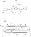
- the source collector module SO may be part of an LPP radiation system as shown in Figure 3 .
- a laser LA is arranged to deposit laser energy into a fuel, such as xenon (Xe), tin (Sn) or lithium (Li), creating the highly ionized plasma 210 with electron temperatures of several 10's of eV.
- Xe xenon
- Sn tin
- Li lithium
- the energetic radiation generated during de-excitation and recombination of these ions is emitted from the plasma, collected by a near normal incidence collector optic CO and focused onto the opening 221 in the enclosing structure 220.
- a chuck is provided for holding by electrostatic force onto a supporting table of a lithography apparatus: a patterning device MA; or a substrate W.
- a chuck may be referred to as an electrostatic chuck.
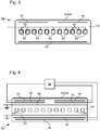
- Figure 4 illustrates an example of such a chuck 43.
- the chuck 43 is mounted on a supporting table MT/WT.
- the supporting table may be referred to as a mask table MT.
- the supporting table may be referred to as a substrate table WT.
- the patterning device MA or substrate W may be heated by the radiation beam of the lithography apparatus.
- Such heating (and/or other thermal loads) can be compensated by driving fluid through temperature conditioning fluid channels 48 formed within the chuck 43.
- the channels may be connected together to form a network for example.
- Various channel configurations are possible to achieve the desired effect of bringing temperature conditioning fluid into contact with the material of the chuck in order to exchange heat with the chuck and thereby control the temperature of the chuck.
- the flow rate and/or temperature of the fluid may be controlled to achieve the desired heat exchange properties and to control the temperature of the chuck.
- the chuck 43 comprises a dielectric member 45.
- the channels 48 in such an embodiment may be formed within the dielectric member 45.
- the chuck 43 further comprises a drive electrode 40, 42 for applying a potential difference between the drive electrode and a first surface 47 of the dielectric member 45.
- the potential difference may be such as to cause a charge to accumulate on the first surface 47.
- the accumulated charge can electrostatically attract and hold a patterning device MA or a substrate W that is brought into contact with the first surface 47.
- This effect is known as the Johnsen-Rahbek effect.
- Chucks/clamps that operate based on this effect may be referred to as Johnsen-Rahbek chucks/clamps, J-R chucks.clamps, or JR chucks/clamps.
- the dielectric member 45 comprises aluminium nitride.
- the dielectric 43 may have a resistivity that is so high that no significant current can pass between the drive electrode 40, 42 and the first surface 27. In this case, the Johnsen-Rahbek effect may not occur to a significant extent. However, an attractive force between the drive electrode 40, 42 and the patterning device MA or substrate W may still occur due to the potential difference between these elements.
- the drive electrode 40, 42 and the patterning device MA or substrate W may act as two plates of a capacitor and be attracted to each other in the same way as the two plates of a charged capacitor. Chucks/clamps that operate predominantly on this principle may be referred to as Coulomb clamps.
- JR clamps will also involve some degree of attraction by the Coulomb mechanism, but the JR effect will normally be dominant in such clamps.
- JR clamps and Coulomb clamps are well known in the field.
- the chuck may be configured so that the patterning device MA or substrate W lies flush against a flat surface of chuck 43. Such an arrangement will tend to favour strong adhesion of the patterning device MA or substrate W to the chuck 43.
- the chuck 43 may be configured so that the patterning device MA or substrate W lies against a plurality of protruding burls. In such an embodiment, the region between the supporting table MT/WT and the patterning device MA or substrate W may be maintained at partial vacuum. Such an arrangement will tend to facilitate removal of the patterning device MA or substrate W, for example because Van der Waals forces acting between the supporting table MT/WT and the patterning device MA or substrate W are less strong.
- two drive electrodes 40 and 42 are provided. This arrangement may be referred to as a bipolar arrangement. In alternative embodiments, a single drive electrode (monopolar) or more than two drive electrodes (multipolar) may be provided. Multipolar Coulomb and JR clamps are known in the field.
- the channels and/or elements of external apparatus that come into contact with the fluid can degrade over time. It has been recognized that at least a component of this degradation may be due to electrolysis effects within the temperature conditioning fluid.
- the electrolysis may occur due to differences in the electric potential on the inside surface of the channels at different positions. Alternatively or additionally, the electrolysis may occur due to a difference in potential between all or a portion of the inside surfaces of the channels within the chuck and one or more elements of external apparatus that come into contact with the fluid.
- Elements that are at different electric potentials and in contact with a given body of fluid may act as electrolysis electrodes.
- the electric field caused by the electrodes may lead to an electric current flowing between the electrodes through the fluid. The electric current can cause electrically stimulated degradation of the material in contact with the fluid and/or of the fluid itself.
- the difference in electric potential stimulates an electro-chemical reaction which degrades machine parts in contact with the fluid.
- the drive electrodes in electrostatic chucks could cause the potential differences and/or currents mentioned above and thereby cause electrolysis and the associated component degradation.
- a shield electrode is provided for reducing or preventing electrolysis effects.
- the shield electrode is connected to ground or earth.
- a shield electrode 60 is provided between the drive electrodes 40, 42 and the channels 48.
- the shield electrode 60 is planar in form.
- the shield electrode 60 is formed from a sheet of metal.
- the shield electrode 60 spans the chuck 43 so as to substantially separate a region of the dielectric member 45 containing the drive electrodes 40, 42 from a region of the dielectric member 45 containing the temperature conditioning fluid channels 48. In this way, the shield electrode 60 can reduce or prevent a voltage applied to the drive electrodes 40, 42 causing a change in the potential at the walls of the channels 48. Electrolysis due to the drive electrodes 40, 42 can thereby be reduced or prevented.
- the chuck 43 may also be clamped to the supporting table MT/WT using an electrostatic force.
- This clamping may be implemented using the Coulomb effect, the JR effect, or both. In the embodiment depicted in Figure 4 , this is achieved by means of a chuck clamping electrode 44 formed adjacent to a second surface 49 of the dielectric member 45.
- a single chuck clamping electrode 44 is provided.
- a plurality of chuck clamping electrodes 44 could be provided.
- a shield electrode 62 is provided between the chuck clamping electrode 44 and the channels 48.
- the shield electrode 62 may be formed in the same way as the shield electrode 60, for example.
- the shield electrode 62 may be configured to substantially separate a region of the dielectric member 45 containing the chuck clamping electrode 44 from a region of the dielectric member 45 containing the channels 48, for example.
- the drive electrode 40 is maintained at a negative potential and the drive electrode 42 is maintained at a positive potential.
- the sizes of the potentials supplied to the drive electrodes 40 and 42 are equal.
- the potentials may be different.
- the clamping electrode 44 is maintained at a positive potential, but this is not essential.
- the chuck clamping electrode may be maintained at a negative potential.
- Figure 5 depicts a chuck 43 according to an alternative embodiment.
- the chuck 43 of Figure 5 is the same as the chuck 43 of Figure 4 except for the configuration of the shield electrodes.
- two planar shield electrodes 60, 62 are provided.
- shield electrodes 64 are instead configured to surround the channels 48.
- the shield electrodes 64 may be formed as a coating on the inner surfaces of the holes in the dielectric member 45 that define the channels 48.
- the shield electrodes 64 are in contact with the fluid in the channels 48 in use or in close proximity to the fluid in the channels 48 in use.
- the shield electrodes 64 of Figure 5 are thus effective for separating the temperature conditioning fluid within the channels from all or a majority of the dielectric member 45 outside of the channels.
- any voltages applied to the drive electrodes 40, 42 or to the chuck clamping electrode 44 cannot cause any significant differences in potential at different positions within the temperature conditioning fluid channels 48.
- the shield electrodes are arranged to be highly conductive, for example metallic, and by virtue of this conductivity will define equipotential or near-equipotential surfaces.
- the shield electrodes 64 are not grounded, there remains the possibility of a difference in potential between the shield electrodes 64 and elements of the apparatus external to the chuck 43 that provides the fluid to the channels 48. This difference in potential could cause electrolysis (electro-chemical reactions) and degradation of the shield electrodes 64, inner surfaces of the channels 48 and/or of components of any external apparatus that are in contact with the fluid in use. It is therefore preferable to connect the shield electrodes 64 to ground, as shown in the example depicted in Figure 5 .
- the shield electrodes are provided primarily to prevent electrolysis effects in the temperature conditioning fluid. However, the shield electrodes may also be configured to reduce or prevent undesirable electrical discharges between the dielectric member 45 and other elements of the lithography apparatus. For example, the shield electrodes may be configured to reduce the voltage on peripheral edges of the chuck 43. This may be achieved by extending the shield members so that they reach the peripheral edges of the dielectric member 45 (as shown in the embodiments of Figures 4 and 6 , for example). The shield electrodes could also be effective for reducing or preventing discharge between the dielectric member 45 and elements protruding through holes, such as holes for mounting pins, that may pass through the dielectric member 45.
- any of the electrodes in the chuck are maintained at an elevated voltage in order to provide electrostatic clamping, resistive heating will occur in the dielectric member 45.
- the chuck 43 is driven in a constant manner (i.e., with stable, constant voltages applied to the drive electrodes and chuck clamping electrode) the dissipated power will also be constant. During such periods it is possible to compensate for the heating relatively accurately using the temperature conditioning fluid channels 48. However, where the dissipated power changes suddenly it may be more difficult to compensate accurately using the temperature conditioning fluid channels 48.
- Rapid changes in the dissipated power will occur, for example, when the drive electrodes 40, 42 are switched off in order to unload and/or load a patterning device MA or substrate W and/or when the drive electrodes 40, 42 are switched back on again. Similarly, it may occasionally be necessary to switch off the chuck clamping electrode 44 and this would also result in a sudden change in the dissipated power in the dielectric member 45.
- Figure 6 depicts an embodiment of a chuck 43 that comprises compensating electrodes 51, 52 and 53 for providing electric currents in the dielectric member 45 that compensate for the absence of heat dissipation when the drive electrodes 40, 42 and the chuck clamping electrode 44, respectively, are switched off.
- the compensating electrodes 51, 52 and 53 are configured to provide a heating within the dielectric member 45 that is equivalent to the heating that would have been provided by driving the drive electrodes 40, 42 and the chuck clamping electrode 44.
- the compensating electrode 51 may be positioned in between the drive electrode 40 and the shield electrode 60.
- the compensating electrode 51 is positioned and shaped such that when the voltage applied to the drive electrode 40 is zero, a voltage can be applied to the compensating electrode 51 that causes a dissipated power in the region between the drive electrode 40 and the shield electrode 60 that is substantially the same as the dissipated power when the drive electrode 40 is switched on.
- One way in which this can be achieved is by positioning the compensating electrode 51 to be equidistant from the drive electrode 40 and the shield electrode 60 and applying a voltage to the compensating electrode 51 that is half the size of the voltage applied to the drive electrode 40 when it is switched on.
- the drive electrode 40 is configured to operate at a voltage Vs when clamping the patterning device MA or substrate W to the chuck 43
- the voltage applied to the compensating electrode 51 when the driving electrode 40 is switched off may be Vs/2.
- the spatial average magnitude of the electric field in the region between the drive electrode 40 and the shield electrode 60 during clamping of a patterning device MA or substrate W may be the same as the spatial average magnitude of the electric field during a period when the drive electrode 40 is switched off, for example during unmounting or mounting of the patterning device MA or substrate W.
- the potential difference between the drive electrode 40 and the compensating electrode 51 (which may be allowed to float during this period) will be 500V because it is positioned halfway between the drive electrode 40 and the grounded shield electrode 60.
- the potential difference between the floating compensating electrode 51 and the shield electrode 60 will also be 500V.
- the voltage thus follows the sequence 1kV - 500V - 0V, from the drive electrode 40 to the floating compensating electrode 51 to the shield electrode 60.
- the compensating electrode 51 is maintained at 1kV/2, i.e., 500V.
- the voltage sequence becomes 0V - 500V - 0V.
- the magnitude of the electric field is thus the same.
- the dissipated power thus remains constant in the region between the drive electrode 40 and the shield electrode 60. Keeping the dissipated power constant facilitates accurate temperature control of the chuck.
- the compensating electrode may be positioned so as not to be equidistant from the drive electrode 40 and the shield electrode 60. In other embodiments, the compensating electrode may be maintained at a voltage other than Vs/2 when the driving electrode 40 is switched off.
- compensating electrodes are provided between both of the drive electrodes 40, 42 and the shield electrode 60 and between the chuck clamping electrode 44 and the shield electrode 62.
- fewer compensating electrodes may be provided.
- the compensating electrode 53 may be omitted.
- the compensating electrode 53 may be of less value than the compensating electrodes 51 and 52 because the chuck 43 may be disconnected from the supporting table WT/MT relatively infrequently in comparison with changes of the patterning device MA or substrate W.
- Figure 6 also depicts an electrode driving system 50 for driving the electrodes within the chuck 43.
- the electrode driving system 50 may be configured to control the voltages applied to one or more of the electrodes and/or to selectively connect one or more of the electrodes to ground as necessary.
- the electrode driving system 50 may be configured to apply a voltage of +/- Vs to the drive electrodes 40, 42, while allowing the compensating electrodes 51 and 52 to float during clamping of the patterning device MA or substrate W.
- the electrode driving system 50 may then be configured to switch the voltages applied to the drive electrodes 40 and 42 to zero and apply a voltage of +/- Vs/2 to the compensating electrodes 51 and 52 to allow unmounting/mounting of the patterning device MA or substrate W.
- the electrode driving system 50 may be configured to apply a voltage Vt to the chuck clamping electrode 44, while allowing the compensating electrode 53 to float, during clamping of the chuck 43 to the supporting table MT/WT.
- the electrode driving system 50 may be configured to apply a zero voltage to the chuck clamping electrode 44 and a voltage of Vt/2 to the compensating electrode 53 when the chuck 43 is to be disconnected from the supporting table MT/WT.
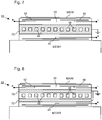
- the dielectric member 45 may form a single integral block of material with the channels 48 being formed directly within the block. This approach may be efficient for manufacturing purposes.
- the chuck body may be formed from a plurality of different materials. The different materials may be bonded together in layers for example. Figures 7 and 8 below provide examples of such arrangements.
- the temperature conditioning fluid channel is separated from the drive electrode or chuck clamping electrode by an electrically insulating element 70 that has a higher resistivity than the resistivity of the dielectric member 45 between the drive electrode 40, 42 and the patterning device MA or substrate W and/or than the dielectric member 45 between the chuck clamping electrode 44 and the supporting table MT/WT.
- the resistivity of the electrically insulating element 70 may be higher than the resistivity that would be required for the dielectric member of a JR clamp.
- the insulating element 70 comprises a region of material within which one or more of the channels 48 are embedded.
- Figure 8 shows an embodiment in which the insulating element 70 comprises a layer separating the drive electrode 40, 42 from the channels 48 and a layer separating the chuck clamping electrode 44 from the channels 48.
- the insulating element 70 comprises a layer separating the drive electrode 40, 42 from the channels 48 and a layer separating the chuck clamping electrode 44 from the channels 48.
- two layers are provided. However, this is not essential. In other embodiments, either or both of the layers may be omitted.
- the insulating element 70 is connected to ground (earth).
- the insulating element 70 reduces or prevents electrical currents from flowing in the region of the channel and therefore reduces or avoids electrolysis effects and reduces resistive heating.
- the chuck 43 is clamped to the supporting table MT/WT electrostatically. However this is not essential.
- the chuck 43 could be clamped to the supporting table MT/WT in other ways.
- the chuck 43 could be clamped to the supporting table MT/WT using glue or optical contacting or brazing or bonding.
- the chuck 43 is formed integrally with the supporting table MT/WT, i.e., the chuck 43 is part of the supporting table MT/WT.
- the chuck 43 may be clamped to the supporting table MT/WT by the same mechanism (e.g., Coulomb or JR) that is used to clamp the patterning device MA or substrate W to the supporting table MT/WT. However this is not essential.
- the chuck 43 could be clamped to the supporting table MT/WT using a different mechanism to that used to clamp the patterning device MA or substrate W to the supporting table MT/WT. For example, the chuck 43 could be clamped to the supporting table MT/WT using a Coulomb clamp while the patterning device MA or substrate W is clamped to the chuck 43 using a JR clamp, or vice versa.
- the time constant of local thermal loads on the chuck during imaging of a die is typically of the order of 0.1 seconds.
- the temperature conditioning provided by the fluid channel typically has a much longer time constant, for example of the order of 10 seconds. Because of this longer time constant, local load effects cannot be completely compensated by the cooling provided by the temperature conditioning fluid. It is possible to use computer modeling to obtain correction factors based on prediction of thermo-mechanical effects. However, the correction cannot be perfect and device performance, for example overlay, remains negatively affected.
- the size of the overlay errors will tend to increase as the total amount of heating caused by the clamping increases. Thus, to achieve a given overlay accuracy it will be necessary to limit the total heating to a particular maximum value.
- This limitation restricts the choice of material that can be used for the body material of the chuck, which is undesirable.
- This limitation also restricts the choice of various operational characteristics relevant for compensating for the heating, such as the required geometry of the temperature conditioning fluid channel, the flow rate of the fluid, the heat capacity of the fluid, the density of the fluid, the thermal conductivity of the fluid, and the kinematic viscosity of the fluid.
- the inventors have recognized that decreasing the size of temperature gradients within the chuck can facilitate more accurate correction of thermo-mechanical effects. Improving the accuracy of the correction reduces the restrictions on the maximum allowable level of heating, and on other operational characteristics relevant to compensating for the heating, for a given level of overlay accuracy.
- the temperature gradients within the chuck are reduced by providing a channel heater that is configured to apply a localized heating in the region of the chuck that defines the temperature conditioning fluid channel 48.
- the localized heating is configured to vary as a function of position along the length of the channel 48.
- the variation in localized heating is achieved by providing the channel heater only along a selected portion of the length of the channel 48. Portions of the length of the channel where the channel heater is not provided will be heated less by the channel heater than portions of the length of the channel where the heater is present.
- the variation in the localized heating is achieved by arranging for the channel heater to provide a variable output power per unit length of the channel heater.
- Figure 9 is a schematic side view showing a chuck corresponding to arrangement of Figure 4 except that channel heaters 84 and 86 have been added. Channel heaters could also be provided to any of the other embodiments discussed above.
- Figure 10 is a schematic top view showing the geometry of the channel 48. Arrow 82 indicates entry of fluid. After entry, the fluid circulates first in a clockwise direction and then in an anticlockwise direction before exiting (arrow 80). The region of the chuck that defines the channel is the region of the chuck directly adjacent to the channel and which defines the cavity through which the fluid flows. In an embodiment, the channel heater is provided along all or a majority of the length of the channel 48 within the chuck.
- the heater is configured to provide an output power that varies as a function of position along the heater in order to provide the variation in the localized heating.
- Figures 9 and 10 illustrate an embodiment of the alternative type in which a channel heater 84,86 is provided only along a selected portion of the length of the channel 48. A higher level of heating is provided at regions along the length of the channel 48 where the channel heater 84,86 is present and a lower level of localized heating or substantially no localized heating is provided at other regions along the length of the channel 48.
- the channel heater 84, 86 is configured to provide the localized heating that varies along the length of the channel in such a way that temperature gradients within the chuck are reduced during use. In an embodiment, this reduction in temperature gradients is achieved by providing a higher level of heating to a region of the chuck defining a first length of the channel (e.g. the length of channel shown in Figure 10 where the channel heater 84 is present) than to a region of the chuck defining a second length of the channel 48 (e.g. in the arrangement of Figure 10 the length of channel between the downstream end of the channel heater 84 and the exit point at arrow 80). In an embodiment of this type, the first length of channel is upstream from the second length of channel.
- a first length of the channel e.g. the length of channel shown in Figure 10 where the channel heater 84 is present
- a second length of the channel 48 e.g. in the arrangement of Figure 10 the length of channel between the downstream end of the channel heater 84 and the exit point at arrow 80.
- This type of arrangement tends to be effective for reducing temperature gradients because the fluid will tend to heat up as it circulates through the chuck. Fluid in upstream regions of the channel 48 (and in portions of the chuck adjacent to the upstream regions) will therefore tend to be cooler than fluid in downstream regions of the channel 48 (and in portions of the chuck adjacent to the downstream regions).
- the channel heater 84,86 By configuring the channel heater 84,86 to compensate this effect it is possible to reduce temperature gradients in the chuck. Reducing temperature gradients facilitates correction of thermo-mechanical effects due to heat loads on the chuck. Device performance, particularly overlay, can therefore be improved.
- the channel heater 84,86 is provided both on the side of the channel 48 that is nearest to the patterning device or substrate MA/W and on the side of the channel 48 opposite to the patterning device or substrate MA/W.
- the channel heater may be provided on one of the two sides only.
- the substrate heater may be configured to surround the channels in a loop or helix, or in any other geometrical configuration that provides the required localized heating that varies along the length of the channel.
- lithographic apparatus in the manufacture of ICs
- the lithographic apparatus described herein may have other applications, such as the manufacture of integrated optical systems, guidance and detection patterns for magnetic domain memories, flat-panel displays, liquid-crystal displays (LCDs), thin-film magnetic heads, etc.
- LCDs liquid-crystal displays
- any use of the terms “wafer” or “die” herein may be considered as synonymous with the more general terms “substrate” or "target portion,”,” respectively.
- the substrate referred to herein may be processed, before or after exposure, in for example a track (a tool that typically applies a layer of resist to a substrate and develops the exposed resist), a metrology tool and/or an inspection tool. Where applicable, the disclosure herein may be applied to such and other substrate processing tools. Further, the substrate may be processed more than once, for example in order to create a multi-layer IC, so that the term substrate used herein may also refer to a substrate that already contains multiple processed layers.
- imprint lithography a topography in a patterning device defines the pattern created on a substrate.
- the topography of the patterning device may be pressed into a layer of resist supplied to the substrate whereupon the resist is cured by applying electromagnetic radiation, heat, pressure or a combination thereof.
- the patterning device is moved out of the resist leaving a pattern in it after the resist is cured.
- lens may refer to any one or combination of various types of optical components, including refractive, reflective, magnetic, electromagnetic and electrostatic optical components.
Description
- This application claims the benefit of
US provisional application 61/544,039, which was filed on 6 October 2011 - The present invention relates to a chuck, a lithographic apparatus and a method of using a chuck.
- A lithographic apparatus is a machine that applies a desired pattern onto a substrate, usually onto a target portion of the substrate. A lithographic apparatus can be used, for example, in the manufacture of integrated circuits (ICs). In that instance, a patterning device, which is alternatively referred to as a mask or a reticle, may be used to generate a circuit pattern to be formed on an individual layer of the IC. This pattern can be transferred onto a target portion (e.g., comprising part of, one, or several dies) on a substrate (e.g., a silicon wafer). Transfer of the pattern is typically via imaging onto a layer of radiation-sensitive material (resist) provided on the substrate. In general, a single substrate will contain a network of adjacent target portions that are successively patterned.
- Lithography is widely recognized as one of the key steps in the manufacture of ICs and other devices and/or structures. However, as the dimensions of features made using lithography become smaller, lithography is becoming a more critical factor for enabling miniature IC or other devices and/or structures to be manufactured.
- A theoretical estimate of the limits of pattern printing can be given by the Rayleigh criterion for resolution as shown in equation (1):

- In order to shorten the exposure wavelength and, thus, reduce the minimum printable size, it has been proposed to use an extreme ultraviolet (EUV) radiation source. EUV radiation is electromagnetic radiation having a wavelength within the range of 10-20 nm, for example within the range of 13-14 nm. It has further been proposed that EUV radiation with a wavelength of less than 10 nm could be used, for example within the range of 5-10 nm such as 6.7 nm or 6.8 nm. Such radiation is termed extreme ultraviolet radiation or soft x-ray radiation. Possible sources include, for example, laser-produced plasma sources, discharge plasma sources, or sources based on synchrotron radiation provided by an electron storage ring.
- EUV radiation may be produced using a plasma. A radiation system for producing EUV radiation may include a laser for exciting a fuel to provide the plasma, and a source collector module for containing the plasma. The plasma may be created, for example, by directing a laser beam at a fuel, such as particles of a suitable material (e.g., tin), or a stream of a suitable gas or vapor, such as Xe gas or Li vapor. The resulting plasma emits output radiation, e.g., EUV radiation, which is collected using a radiation collector. The radiation collector may be a mirrored normal incidence radiation collector, which receives the radiation and focuses the radiation into a beam. The source collector module may include an enclosing structure or chamber arranged to provide a vacuum environment to support the plasma. Such a radiation system is typically termed a laser produced plasma (LPP) source.
- A chuck may be provided for holding a patterning device for imparting a radiation beam with a pattern in its cross section or a substrate for receiving the patterned radiation beam. The chuck may be configured to hold the patterning device or substrate by electrostatic attraction. The chuck may provide Johnsen-Rahbek (JR) clamping, Coulomb clamping, or both, for example. The temperature of the chuck may be controlled by driving a temperature conditioning fluid through channels formed within the chuck. It has been found in such arrangements that the interior walls of the channels, and/or of apparatus external to the chuck that is in contact with the fluid, can degrade over time. It has also been found that electric current formed within the chuck during operation can lead to resistive heatingof the chuck. Such heating can be compensated by the fluid in the channels. However, it can be difficult to compensate for sudden changes in the dissipated power, for example when the chuck is turned off to unmount a patterning device or substrate.
-
US 2009/207392 A discloses a lithographic apparatus configured to transfer a pattern from a patterning structure, held by a patterning structure holder, onto a substrate that is held by a substrate holder. The apparatus includes a first object holder configured to hold an object, and an object temperature conditioner configured to condition a temperature of the object prior to and/or during transfer of the objection to the first object holder. The object temperature conditioner includes a second object holder having a fluid duct system and an electrical temperature conditioner. -
WO 92/20093 A -
US 2005/134828 A , which relates to lithography apparatus, discloses a channel structure comprising a shielding layer for shielding the channel structure from an electrostatic field. - It is desirable to at least partially address one or more of the abovementioned problems. For example, it is desirable to provide an arrangement in which the channels and/or external apparatus that is in contact with the fluid do not degrade over time. For example, it is desirable to avoid changes in temperature of the chuck during unmounting and mounting of the patterning device or substrate.
- The scope of the invention is defined in the appended claims.
- Embodiments of the invention will now be described, by way of example only, with reference to the accompanying schematic drawings in which corresponding reference symbols indicate corresponding parts, and in which:
-
Figure 1 depicts a lithographic apparatus according to an embodiment of the invention; -
Figure 2 is a more detailed view of theapparatus 100; -
Figure 3 is a more detailed view of the source collector module SO of the apparatus ofFigures 1 and 2 ; -
Figure 4 depicts an electrostatic chuck comprising two drive electrodes, a chuck clamping electrode, temperature conditioning fluid channels, and two planar shield electrodes; -
Figure 5 depicts an electrostatic chuck comprising shield electrodes surrounding temperature conditioning fluid channels; -
Figure 6 depicts an electrostatic chuck further comprising two compensating electrodes and an electrode driving system; -
Figure 7 depicts an electrostatic chuck further comprising an insulating element surrounding the temperature conditioning fluid channels; -
Figure 8 depicts an electrostatic chuck further comprising an insulating element in the form of layers between the drive electrode and the channels and between the chuck clamping electrode and the channels. -
Figure 9 depicts an electrostatic chuck of the type illustrated inFigure 4 , further comprising a channel heater. -
Figure 10 is a schematic top view of the embodiment ofFigure 9 showing the geometry of the temperature conditioning fluid channel and the associated channel heater. - The features and advantages of the present invention will become more apparent from the detailed description set forth below when taken in conjunction with the drawings, in which like reference characters identify corresponding elements throughout. In the drawings, like reference numbers generally indicate identical, functionally similar, and/or structurally similar elements. The drawing in which an element first appears is indicated by the leftmost digit(s) in the corresponding reference number
-
Figure 1 schematically depicts alithographic apparatus 100 including a source collector module SO according to one embodiment of the invention. The apparatus comprises: - an illumination system (illuminator) IL configured to condition a radiation beam B (e.g., EUV radiation).
- a support structure (e.g., a mask table) MT constructed to support a patterning device (e.g., a mask or a reticle) MA and connected to a first positioner PM configured to accurately position the patterning device;
- a substrate table (e.g., a wafer table) WT constructed to hold a substrate (e.g., a resist-coated wafer) W and connected to a second positioner PW configured to accurately position the substrate; and
- a projection system (e.g., a reflective projection system) PS configured to project a pattern imparted to the radiation beam B by patterning device MA onto a target portion C (e.g., comprising one or more dies) of the substrate W.
- The illumination system may include various types of optical components, such as refractive, reflective, magnetic, electromagnetic, electrostatic or other types of optical components, or any combination thereof, for directing, shaping, or controlling radiation.
- The support structure MT holds the patterning device MA in a manner that depends on the orientation of the patterning device, the design of the lithographic apparatus, and other conditions, such as for example whether or not the patterning device is held in a vacuum environment. The support structure can use mechanical, vacuum, electrostatic or other clamping techniques to hold the patterning device. The support structure may be a frame or a table, for example, which may be fixed or movable as required. The support structure may ensure that the patterning device is at a desired position, for example with respect to the projection system.
- The term "patterning device" should be broadly interpreted as referring to any device that can be used to impart a radiation beam with a pattern in its cross-section such as to create a pattern in a target portion of the substrate. The pattern imparted to the radiation beam may correspond to a particular functional layer in a device being created in the target portion, such as an integrated circuit.
- The patterning device may be transmissive or reflective. Examples of patterning devices include masks, programmable mirror arrays, and programmable LCD panels. Masks are well known in lithography, and include mask types such as binary, alternating phase-shift, and attenuated phase-shift, as well as various hybrid mask types. An example of a programmable mirror array employs a matrix arrangement of small mirrors, each of which can be individually tilted so as to reflect an incoming radiation beam in different directions. The tilted mirrors impart a pattern in a radiation beam, which is reflected by the mirror matrix.
- The projection system, like the illumination system, may include various types of optical components, such as refractive, reflective, magnetic, electromagnetic, electrostatic or other types of optical components, or any combination thereof, as appropriate for the exposure radiation being used, or for other factors such as the use of a vacuum. It may be desired to use a vacuum for EUV radiation since other gases may absorb too much radiation. A vacuum environment may therefore be provided to the whole beam path with the aid of a vacuum wall and vacuum pumps.
- As here depicted, the apparatus is of a reflective type (e.g., employing a reflective mask).
- The lithographic apparatus may be of a type having two (dual stage) or more substrate tables (and/or two or more mask tables). In such "multiple stage" machines the additional tables may be used in parallel, or preparatory steps may be carried out on one or more tables while one or more other tables are being used for exposure.
- Referring to
Figure 1 , the illuminator IL receives an extreme ultra violet radiation beam from the source collector module SO. Methods to produce EUV light include, but are not necessarily limited to, converting a material into a plasma state that has at least one element, e.g., xenon, lithium or tin, with one or more emission lines in the EUV range. In one such method, often termed laser produced plasma ("LPP") the required plasma can be produced by irradiating a fuel, such as a droplet, stream or cluster of material having the required line-emitting element, with a laser beam. The source collector module SO may be part of an EUV radiation system including a laser, not shown inFigure 1 , for providing the laser beam exciting the fuel. The resulting plasma emits output radiation, e.g., EUV radiation, which is collected using a radiation collector, disposed in the source collector module. The laser and the source collector module may be separate entities, for example when a CO2 laser is used to provide the laser beam for fuel excitation. - In such cases, the laser is not considered to form part of the lithographic apparatus and the radiation beam is passed from the laser to the source collector module with the aid of a beam delivery system comprising, for example, suitable directing mirrors and/or a beam expander. In other cases the source may be an integral part of the source collector module, for example when the source is a discharge produced plasma EUV generator, often termed as a DPP source.
- The illuminator IL may comprise an adjuster for adjusting the angular intensity distribution of the radiation beam. Generally, at least the outer and/or inner radial extent (commonly referred to as -outer and -inner, respectively) of the intensity distribution in a pupil plane of the illuminator can be adjusted. In addition, the illuminator IL may comprise various other components, such as facetted field and pupil mirror devices. The illuminator may be used to condition the radiation beam, to have a desired uniformity and intensity distribution in its cross-section.
- The radiation beam B is incident on the patterning device (e.g., mask) MA, which is held on the support structure (e.g., mask table) MT, and is patterned by the patterning device. After being reflected from the patterning device (e.g., mask) MA, the radiation beam B passes through the projection system PS, which focuses the beam onto a target portion C of the substrate W. With the aid of the second positioner PW and position sensor PS2 (e.g., an interferometric device, linear encoder or capacitive sensor), the substrate table WT can be moved accurately, e.g., so as to position different target portions C in the path of the radiation beam B. Similarly, the first positioner PM and another position sensor PS 1 can be used to accurately position the patterning device (e.g., mask) MA with respect to the path of the radiation beam B. Patterning device (e.g., mask) MA and substrate W may be aligned using mask alignment marks M1, M2 and substrate alignment marks P1, P2.
- The depicted apparatus could be used in at least one of the following modes:
- 1. In step mode, the support structure (e.g., mask table) MT and the substrate table WT are kept essentially stationary, while an entire pattern imparted to the radiation beam is projected onto a target portion C at one time (i.e., a single static exposure). The substrate table WT is then shifted in the X and/or Y direction so that a different target portion C can be exposed.
- 2. In scan mode, the support structure (e.g., mask table) MT and the substrate table WT are scanned synchronously while a pattern imparted to the radiation beam is projected onto a target portion C (i.e., a single dynamic exposure). The velocity and direction of the substrate table WT relative to the support structure (e.g., mask table) MT may be determined by the (de-)magnification and image reversal characteristics of the projection system PS.
- 3. In another mode, the support structure (e.g., mask table) MT is kept essentially stationary holding a programmable patterning device, and the substrate table WT is moved or scanned while a pattern imparted to the radiation beam is projected onto a target portion C. In this mode, generally a pulsed radiation source is employed and the programmable patterning device is updated as required after each movement of the substrate table WT or in between successive radiation pulses during a scan. This mode of operation can be readily applied to maskless lithography that utilizes programmable patterning device, such as a programmable mirror array of a type as referred to above.
- Combinations and/or variations on the above described modes of use or entirely different modes of use may also be employed.
-
Figure 2 shows theapparatus 100 in more detail, including the source collector module SO, the illumination system IL, and the projection system PS. The source collector module SO is constructed and arranged such that a vacuum environment can be maintained in an enclosingstructure 220 of the source collector module SO. An EUVradiation emitting plasma 210 may be formed by a discharge produced plasma source. EUV radiation may be produced by a gas or vapor, for example Xe gas, Li vapor or Sn vapor in which the veryhot plasma 210 is created to emit radiation in the EUV range of the electromagnetic spectrum. The veryhot plasma 210 is created by, for example, an electrical discharge causing an at least partially ionized plasma. Partial pressures of, for example, 10 Pa of Xe, Li, Sn vapor or any other suitable gas or vapor may be required for efficient generation of the radiation. In an embodiment, a plasma of excited tin (Sn) is provided to produce EUV radiation. - The radiation emitted by the
hot plasma 210 is passed from asource chamber 211 into acollector chamber 212 via an optional gas barrier or contaminant trap 230 (in some cases also referred to as contaminant barrier or foil trap) that is positioned in or behind an opening insource chamber 211. Thecontaminant trap 230 may include a channel structure.Contamination trap 230 may also include a gas barrier or a combination of a gas barrier and a channel structure. The contaminant trap orcontaminant barrier 230 further indicated herein at least includes a channel structure, as known in the art. - The
collector chamber 211 may include a radiation collector CO, which may be a so-called grazing incidence collector. Radiation collector CO has an upstreamradiation collector side 251 and a downstreamradiation collector side 252. Radiation that traverses collector CO can be reflected off a gratingspectral filter 240 to be focused in a virtual source point IF. The virtual source point IF is commonly referred to as the intermediate focus, and the source collector module is arranged such that the intermediate focus IF is located at or near anopening 221 in the enclosingstructure 220. The virtual source point IF is an image of theradiation emitting plasma 210. - Subsequently the radiation traverses the illumination system IL, which may include a facetted
field mirror device 22 and a facettedpupil mirror device 24 arranged to provide a desired angular distribution of theradiation beam 21, at the patterning device MA, as well as a desired uniformity of radiation intensity at the patterning device MA. Upon reflection of the beam ofradiation 21 at the patterning device MA, held by the support structure MT, a patternedbeam 26 is formed and the patternedbeam 26 is imaged by the projection system PS viareflective elements - More elements than shown may generally be present in illumination optics unit IL and projection system PS. The grating
spectral filter 240 may optionally be present, depending upon the type of lithographic apparatus. Further, there may be more mirrors present than those shown in the Figures, for example there may be 1- 6 additional reflective elements present in the projection system PS than shown inFigure 2 . - Collector optic CO, as illustrated in
Figure 2 , is depicted as a nested collector withgrazing incidence reflectors grazing incidence reflectors - Alternatively, the source collector module SO may be part of an LPP radiation system as shown in
Figure 3 . A laser LA is arranged to deposit laser energy into a fuel, such as xenon (Xe), tin (Sn) or lithium (Li), creating the highly ionizedplasma 210 with electron temperatures of several 10's of eV. The energetic radiation generated during de-excitation and recombination of these ions is emitted from the plasma, collected by a near normal incidence collector optic CO and focused onto theopening 221 in the enclosingstructure 220. - In an embodiment, a chuck is provided for holding by electrostatic force onto a supporting table of a lithography apparatus: a patterning device MA; or a substrate W. Such a chuck may be referred to as an electrostatic chuck.
Figure 4 illustrates an example of such achuck 43. In the embodiment shown, thechuck 43 is mounted on a supporting table MT/WT. Where thechuck 43 is configured to support a patterning device MA, the supporting table may be referred to as a mask table MT. Where thechuck 43 is configured to hold a substrate W, the supporting table may be referred to as a substrate table WT. - During use the patterning device MA or substrate W may be heated by the radiation beam of the lithography apparatus. Such heating (and/or other thermal loads) can be compensated by driving fluid through temperature
conditioning fluid channels 48 formed within thechuck 43. The channels may be connected together to form a network for example. Various channel configurations are possible to achieve the desired effect of bringing temperature conditioning fluid into contact with the material of the chuck in order to exchange heat with the chuck and thereby control the temperature of the chuck. The flow rate and/or temperature of the fluid may be controlled to achieve the desired heat exchange properties and to control the temperature of the chuck. - In an embodiment, the
chuck 43 comprises adielectric member 45. Thechannels 48 in such an embodiment may be formed within thedielectric member 45. - In an embodiment, the
chuck 43 further comprises adrive electrode first surface 47 of thedielectric member 45. The potential difference may be such as to cause a charge to accumulate on thefirst surface 47. The accumulated charge can electrostatically attract and hold a patterning device MA or a substrate W that is brought into contact with thefirst surface 47. This effect is known as the Johnsen-Rahbek effect. Chucks/clamps that operate based on this effect may be referred to as Johnsen-Rahbek chucks/clamps, J-R chucks.clamps, or JR chucks/clamps. In an embodiment, thedielectric member 45 comprises aluminium nitride. - In an embodiment, the dielectric 43 may have a resistivity that is so high that no significant current can pass between the
drive electrode drive electrode drive electrode - JR clamps will also involve some degree of attraction by the Coulomb mechanism, but the JR effect will normally be dominant in such clamps.
- JR clamps and Coulomb clamps are well known in the field.
- In an embodiment, the chuck may be configured so that the patterning device MA or substrate W lies flush against a flat surface of
chuck 43. Such an arrangement will tend to favour strong adhesion of the patterning device MA or substrate W to thechuck 43. In an alternative embodiment, thechuck 43 may be configured so that the patterning device MA or substrate W lies against a plurality of protruding burls. In such an embodiment, the region between the supporting table MT/WT and the patterning device MA or substrate W may be maintained at partial vacuum. Such an arrangement will tend to facilitate removal of the patterning device MA or substrate W, for example because Van der Waals forces acting between the supporting table MT/WT and the patterning device MA or substrate W are less strong. - In the embodiment shown, two
drive electrodes - As mentioned above, in electrostatic chucks comprising temperature conditioning fluid channels, the channels and/or elements of external apparatus that come into contact with the fluid can degrade over time. It has been recognized that at least a component of this degradation may be due to electrolysis effects within the temperature conditioning fluid. The electrolysis may occur due to differences in the electric potential on the inside surface of the channels at different positions. Alternatively or additionally, the electrolysis may occur due to a difference in potential between all or a portion of the inside surfaces of the channels within the chuck and one or more elements of external apparatus that come into contact with the fluid. Elements that are at different electric potentials and in contact with a given body of fluid may act as electrolysis electrodes. The electric field caused by the electrodes may lead to an electric current flowing between the electrodes through the fluid. The electric current can cause electrically stimulated degradation of the material in contact with the fluid and/or of the fluid itself. Thus, the difference in electric potential stimulates an electro-chemical reaction which degrades machine parts in contact with the fluid.
- The drive electrodes in electrostatic chucks could cause the potential differences and/or currents mentioned above and thereby cause electrolysis and the associated component degradation.
- In an embodiment, a shield electrode is provided for reducing or preventing electrolysis effects. Preferably the shield electrode is connected to ground or earth.
- In the embodiment shown in
Figure 4 , ashield electrode 60 is provided between thedrive electrodes channels 48. In the embodiment shown, theshield electrode 60 is planar in form. In an embodiment, theshield electrode 60 is formed from a sheet of metal. In an embodiment, theshield electrode 60 spans thechuck 43 so as to substantially separate a region of thedielectric member 45 containing thedrive electrodes dielectric member 45 containing the temperatureconditioning fluid channels 48. In this way, theshield electrode 60 can reduce or prevent a voltage applied to thedrive electrodes channels 48. Electrolysis due to thedrive electrodes - In an embodiment, the
chuck 43 may also be clamped to the supporting table MT/WT using an electrostatic force. This clamping may be implemented using the Coulomb effect, the JR effect, or both. In the embodiment depicted inFigure 4 , this is achieved by means of achuck clamping electrode 44 formed adjacent to asecond surface 49 of thedielectric member 45. In the example shown, a singlechuck clamping electrode 44 is provided. However, in alternative embodiments, a plurality ofchuck clamping electrodes 44 could be provided. In order to prevent a voltage applied to thechuck clamping electrode 44 from leading to electrolysis within the temperature conditioning fluid, ashield electrode 62 is provided between thechuck clamping electrode 44 and thechannels 48. Theshield electrode 62 may be formed in the same way as theshield electrode 60, for example. Theshield electrode 62 may be configured to substantially separate a region of thedielectric member 45 containing thechuck clamping electrode 44 from a region of thedielectric member 45 containing thechannels 48, for example. - In the embodiment illustrated in
Figure 4 , during clamping of a patterning device MA or substrate W thedrive electrode 40 is maintained at a negative potential and thedrive electrode 42 is maintained at a positive potential. In an embodiment, the sizes of the potentials supplied to thedrive electrodes electrode 44 is maintained at a positive potential, but this is not essential. In alternative embodiments, the chuck clamping electrode may be maintained at a negative potential. -
Figure 5 depicts achuck 43 according to an alternative embodiment. Thechuck 43 ofFigure 5 is the same as thechuck 43 ofFigure 4 except for the configuration of the shield electrodes. InFigure 4 , twoplanar shield electrodes Figure 5 ,shield electrodes 64 are instead configured to surround thechannels 48. For example, theshield electrodes 64 may be formed as a coating on the inner surfaces of the holes in thedielectric member 45 that define thechannels 48. Preferably theshield electrodes 64 are in contact with the fluid in thechannels 48 in use or in close proximity to the fluid in thechannels 48 in use. Theshield electrodes 64 ofFigure 5 are thus effective for separating the temperature conditioning fluid within the channels from all or a majority of thedielectric member 45 outside of the channels. Therefore, any voltages applied to thedrive electrodes chuck clamping electrode 44 cannot cause any significant differences in potential at different positions within the temperatureconditioning fluid channels 48. Indeed, in an embodiment the shield electrodes are arranged to be highly conductive, for example metallic, and by virtue of this conductivity will define equipotential or near-equipotential surfaces. - If the
shield electrodes 64 are not grounded, there remains the possibility of a difference in potential between theshield electrodes 64 and elements of the apparatus external to thechuck 43 that provides the fluid to thechannels 48. This difference in potential could cause electrolysis (electro-chemical reactions) and degradation of theshield electrodes 64, inner surfaces of thechannels 48 and/or of components of any external apparatus that are in contact with the fluid in use. It is therefore preferable to connect theshield electrodes 64 to ground, as shown in the example depicted inFigure 5 . - The shield electrodes are provided primarily to prevent electrolysis effects in the temperature conditioning fluid. However, the shield electrodes may also be configured to reduce or prevent undesirable electrical discharges between the
dielectric member 45 and other elements of the lithography apparatus. For example, the shield electrodes may be configured to reduce the voltage on peripheral edges of thechuck 43. This may be achieved by extending the shield members so that they reach the peripheral edges of the dielectric member 45 (as shown in the embodiments ofFigures 4 and6 , for example). The shield electrodes could also be effective for reducing or preventing discharge between thedielectric member 45 and elements protruding through holes, such as holes for mounting pins, that may pass through thedielectric member 45. - When any of the electrodes in the chuck are maintained at an elevated voltage in order to provide electrostatic clamping, resistive heating will occur in the
dielectric member 45. When thechuck 43 is driven in a constant manner (i.e., with stable, constant voltages applied to the drive electrodes and chuck clamping electrode) the dissipated power will also be constant. During such periods it is possible to compensate for the heating relatively accurately using the temperatureconditioning fluid channels 48. However, where the dissipated power changes suddenly it may be more difficult to compensate accurately using the temperatureconditioning fluid channels 48. Rapid changes in the dissipated power will occur, for example, when thedrive electrodes drive electrodes chuck clamping electrode 44 and this would also result in a sudden change in the dissipated power in thedielectric member 45. -
Figure 6 depicts an embodiment of achuck 43 that comprises compensatingelectrodes dielectric member 45 that compensate for the absence of heat dissipation when thedrive electrodes chuck clamping electrode 44, respectively, are switched off. The compensatingelectrodes dielectric member 45 that is equivalent to the heating that would have been provided by driving thedrive electrodes chuck clamping electrode 44. - The compensating
electrode 51 may be positioned in between thedrive electrode 40 and theshield electrode 60. In an embodiment, the compensatingelectrode 51 is positioned and shaped such that when the voltage applied to thedrive electrode 40 is zero, a voltage can be applied to the compensatingelectrode 51 that causes a dissipated power in the region between thedrive electrode 40 and theshield electrode 60 that is substantially the same as the dissipated power when thedrive electrode 40 is switched on. One way in which this can be achieved is by positioning the compensatingelectrode 51 to be equidistant from thedrive electrode 40 and theshield electrode 60 and applying a voltage to the compensatingelectrode 51 that is half the size of the voltage applied to thedrive electrode 40 when it is switched on. For example, if thedrive electrode 40 is configured to operate at a voltage Vs when clamping the patterning device MA or substrate W to thechuck 43, the voltage applied to the compensatingelectrode 51 when the drivingelectrode 40 is switched off may be Vs/2. In this way, the spatial average magnitude of the electric field in the region between thedrive electrode 40 and theshield electrode 60 during clamping of a patterning device MA or substrate W may be the same as the spatial average magnitude of the electric field during a period when thedrive electrode 40 is switched off, for example during unmounting or mounting of the patterning device MA or substrate W. For example, if thedrive electrode 40 is maintained at a voltage of 1kV when switched on, the potential difference between thedrive electrode 40 and the compensating electrode 51 (which may be allowed to float during this period) will be 500V because it is positioned halfway between thedrive electrode 40 and the groundedshield electrode 60. The potential difference between the floating compensatingelectrode 51 and theshield electrode 60 will also be 500V. The voltage thus follows the sequence 1kV - 500V - 0V, from thedrive electrode 40 to the floating compensatingelectrode 51 to theshield electrode 60. When thedrive electrode 40 is switched to 0V (i.e., switched off) or connected to ground the compensatingelectrode 51 is maintained at 1kV/2, i.e., 500V. Thus, the voltage sequence becomes 0V - 500V - 0V. The magnitude of the electric field is thus the same. The dissipated power thus remains constant in the region between thedrive electrode 40 and theshield electrode 60. Keeping the dissipated power constant facilitates accurate temperature control of the chuck. - In other embodiments, the compensating electrode may be positioned so as not to be equidistant from the
drive electrode 40 and theshield electrode 60. In other embodiments, the compensating electrode may be maintained at a voltage other than Vs/2 when the drivingelectrode 40 is switched off. - The above discussion concerning operation of the compensating
electrode 51 between thedrive electrode 40 and theshield electrode 60 applies, with the necessary changes as would become apparent to a person having ordinary skill in the art, to the compensatingelectrode 52 between thedrive electrode 42 and theshield electrode 60 and to the compensatingelectrode 53 between thechuck clamping electrode 44 and theshield electrode 62. - In the example depicted in
Figure 6 , compensating electrodes are provided between both of thedrive electrodes shield electrode 60 and between thechuck clamping electrode 44 and theshield electrode 62. However, in other embodiments fewer compensating electrodes may be provided. For example, the compensatingelectrode 53 may be omitted. In some embodiments the compensatingelectrode 53 may be of less value than the compensatingelectrodes chuck 43 may be disconnected from the supporting table WT/MT relatively infrequently in comparison with changes of the patterning device MA or substrate W. -
Figure 6 also depicts anelectrode driving system 50 for driving the electrodes within thechuck 43. Theelectrode driving system 50 may be configured to control the voltages applied to one or more of the electrodes and/or to selectively connect one or more of the electrodes to ground as necessary. For example, theelectrode driving system 50 may be configured to apply a voltage of +/- Vs to thedrive electrodes electrodes electrode driving system 50 may then be configured to switch the voltages applied to thedrive electrodes electrodes electrode driving system 50 may be configured to apply a voltage Vt to thechuck clamping electrode 44, while allowing the compensatingelectrode 53 to float, during clamping of thechuck 43 to the supporting table MT/WT. Theelectrode driving system 50 may be configured to apply a zero voltage to thechuck clamping electrode 44 and a voltage of Vt/2 to the compensatingelectrode 53 when thechuck 43 is to be disconnected from the supporting table MT/WT. - In the embodiments discussed above, the
dielectric member 45 may form a single integral block of material with thechannels 48 being formed directly within the block. This approach may be efficient for manufacturing purposes. However, in alternative embodiments, the chuck body may be formed from a plurality of different materials. The different materials may be bonded together in layers for example.Figures 7 and 8 below provide examples of such arrangements. - In an embodiment, the temperature conditioning fluid channel is separated from the drive electrode or chuck clamping electrode by an electrically insulating
element 70 that has a higher resistivity than the resistivity of thedielectric member 45 between thedrive electrode dielectric member 45 between thechuck clamping electrode 44 and the supporting table MT/WT. For example, the resistivity of the electrically insulatingelement 70 may be higher than the resistivity that would be required for the dielectric member of a JR clamp. - In
Figure 7 the insulatingelement 70 comprises a region of material within which one or more of thechannels 48 are embedded. -
Figure 8 shows an embodiment in which the insulatingelement 70 comprises a layer separating thedrive electrode channels 48 and a layer separating thechuck clamping electrode 44 from thechannels 48. In the arrangement shown, two layers are provided. However, this is not essential. In other embodiments, either or both of the layers may be omitted. - In an embodiment, the insulating
element 70 is connected to ground (earth). - The insulating
element 70 reduces or prevents electrical currents from flowing in the region of the channel and therefore reduces or avoids electrolysis effects and reduces resistive heating. - In the examples discussed above the
chuck 43 is clamped to the supporting table MT/WT electrostatically. However this is not essential. Thechuck 43 could be clamped to the supporting table MT/WT in other ways. For example thechuck 43 could be clamped to the supporting table MT/WT using glue or optical contacting or brazing or bonding. In an embodiment, thechuck 43 is formed integrally with the supporting table MT/WT, i.e., thechuck 43 is part of the supporting table MT/WT. - The
chuck 43 may be clamped to the supporting table MT/WT by the same mechanism (e.g., Coulomb or JR) that is used to clamp the patterning device MA or substrate W to the supporting table MT/WT. However this is not essential. Thechuck 43 could be clamped to the supporting table MT/WT using a different mechanism to that used to clamp the patterning device MA or substrate W to the supporting table MT/WT. For example, thechuck 43 could be clamped to the supporting table MT/WT using a Coulomb clamp while the patterning device MA or substrate W is clamped to thechuck 43 using a JR clamp, or vice versa. - The time constant of local thermal loads on the chuck during imaging of a die is typically of the order of 0.1 seconds. The temperature conditioning provided by the fluid channel typically has a much longer time constant, for example of the order of 10 seconds. Because of this longer time constant, local load effects cannot be completely compensated by the cooling provided by the temperature conditioning fluid. It is possible to use computer modeling to obtain correction factors based on prediction of thermo-mechanical effects. However, the correction cannot be perfect and device performance, for example overlay, remains negatively affected.
- During clamping of a wafer, heat dissipation in the chuck will cause heat to be transferred to the fluid in the channels. This will tend to cause a temperature gradient along the fluid in the channels and along the region of the chuck defining the channels that is adjacent to the fluid. During phases where the wafer is unclamped an extra heater may be used to provide an equivalent heating so that the contribution to temperature gradients from heating of the chuck remains constant. Friction between the fluid and the walls of the channel may also cause heating of the fluid and walls. Such friction causes a pressure drop along the channel. The size of the pressure drop can provide a measure of the amount of heating due to this mechanism. This frictional heating also contributes to the temperature gradient along the fluid in the channels and along the region of the chuck defining the channels.
- Keeping temperature gradients in the chuck constant facilitates software-based correction of thermo-mechanical effects but is not sufficient to enable perfect correction.
- The size of the overlay errors will tend to increase as the total amount of heating caused by the clamping increases. Thus, to achieve a given overlay accuracy it will be necessary to limit the total heating to a particular maximum value. This limitation restricts the choice of material that can be used for the body material of the chuck, which is undesirable. This limitation also restricts the choice of various operational characteristics relevant for compensating for the heating, such as the required geometry of the temperature conditioning fluid channel, the flow rate of the fluid, the heat capacity of the fluid, the density of the fluid, the thermal conductivity of the fluid, and the kinematic viscosity of the fluid.
- The inventors have recognized that decreasing the size of temperature gradients within the chuck can facilitate more accurate correction of thermo-mechanical effects. Improving the accuracy of the correction reduces the restrictions on the maximum allowable level of heating, and on other operational characteristics relevant to compensating for the heating, for a given level of overlay accuracy.
- In an embodiment, the temperature gradients within the chuck are reduced by providing a channel heater that is configured to apply a localized heating in the region of the chuck that defines the temperature
conditioning fluid channel 48. The localized heating is configured to vary as a function of position along the length of thechannel 48. In an embodiment, the variation in localized heating is achieved by providing the channel heater only along a selected portion of the length of thechannel 48. Portions of the length of the channel where the channel heater is not provided will be heated less by the channel heater than portions of the length of the channel where the heater is present. Alternatively or additionally, the variation in the localized heating is achieved by arranging for the channel heater to provide a variable output power per unit length of the channel heater. - An example configuration is illustrated in
Figures 9 and 10. Figure 9 is a schematic side view showing a chuck corresponding to arrangement ofFigure 4 except thatchannel heaters Figure 10 is a schematic top view showing the geometry of thechannel 48.Arrow 82 indicates entry of fluid. After entry, the fluid circulates first in a clockwise direction and then in an anticlockwise direction before exiting (arrow 80). The region of the chuck that defines the channel is the region of the chuck directly adjacent to the channel and which defines the cavity through which the fluid flows. In an embodiment, the channel heater is provided along all or a majority of the length of thechannel 48 within the chuck. In an embodiment of this type, the heater is configured to provide an output power that varies as a function of position along the heater in order to provide the variation in the localized heating.Figures 9 and 10 illustrate an embodiment of the alternative type in which achannel heater channel 48. A higher level of heating is provided at regions along the length of thechannel 48 where thechannel heater channel 48. - In an embodiment, the
channel heater Figure 10 where thechannel heater 84 is present) than to a region of the chuck defining a second length of the channel 48 (e.g. in the arrangement ofFigure 10 the length of channel between the downstream end of thechannel heater 84 and the exit point at arrow 80). In an embodiment of this type, the first length of channel is upstream from the second length of channel. This type of arrangement tends to be effective for reducing temperature gradients because the fluid will tend to heat up as it circulates through the chuck. Fluid in upstream regions of the channel 48 (and in portions of the chuck adjacent to the upstream regions) will therefore tend to be cooler than fluid in downstream regions of the channel 48 (and in portions of the chuck adjacent to the downstream regions). By configuring thechannel heater - In the embodiment shown in
Figures 9 and 10 , thechannel heater channel 48 that is nearest to the patterning device or substrate MA/W and on the side of thechannel 48 opposite to the patterning device or substrate MA/W. However, this is not essential. In other embodiments, the channel heater may be provided on one of the two sides only. Alternatively, the substrate heater may be configured to surround the channels in a loop or helix, or in any other geometrical configuration that provides the required localized heating that varies along the length of the channel. - Although specific reference may be made in this text to the use of lithographic apparatus in the manufacture of ICs, it should be understood that the lithographic apparatus described herein may have other applications, such as the manufacture of integrated optical systems, guidance and detection patterns for magnetic domain memories, flat-panel displays, liquid-crystal displays (LCDs), thin-film magnetic heads, etc. The skilled artisan will appreciate that, in the context of such alternative applications, any use of the terms "wafer" or "die" herein may be considered as synonymous with the more general terms "substrate" or "target portion,"," respectively. The substrate referred to herein may be processed, before or after exposure, in for example a track (a tool that typically applies a layer of resist to a substrate and develops the exposed resist), a metrology tool and/or an inspection tool. Where applicable, the disclosure herein may be applied to such and other substrate processing tools. Further, the substrate may be processed more than once, for example in order to create a multi-layer IC, so that the term substrate used herein may also refer to a substrate that already contains multiple processed layers.
- Although specific reference may have been made above to the use of embodiments of the invention in the context of optical lithography, it will be appreciated that the invention may be used in other applications, for example imprint lithography, and where the context allows, is not limited to optical lithography. In imprint lithography a topography in a patterning device defines the pattern created on a substrate. The topography of the patterning device may be pressed into a layer of resist supplied to the substrate whereupon the resist is cured by applying electromagnetic radiation, heat, pressure or a combination thereof. The patterning device is moved out of the resist leaving a pattern in it after the resist is cured.
- The term "lens," where the context allows, may refer to any one or combination of various types of optical components, including refractive, reflective, magnetic, electromagnetic and electrostatic optical components.
- While specific embodiments of the invention have been described above, it will be appreciated that the invention may be practiced otherwise than as described. The descriptions above are intended to be illustrative, not limiting. Thus it will be apparent to one skilled in the art that modifications may be made to the invention as described without departing from the scope of the claims set out below.
Claims (15)
- A chuck (43) for use in holding a patterning device (MA) or a substrate onto a supporting table (MT/WT) of a lithography apparatus (100) by electrostatic force, in which the patterning device is for imparting a radiation beam with a pattern in its cross-section to form a patterned radiation beam, and the substrate (W) is for receiving the patterned radiation beam;
said chuck (43) comprising:a dielectric member (45);a temperature conditioning fluid channel (48) formed within the dielectric member (45);a drive electrode (40,42) for applying a potential difference between the drive electrode (40, 42) and the patterning device (MA) or substrate (W) across the dielectric member (45) in order to electrostatically attract the patterning device (MA) or substrate (W) towards the drive electrode (40, 42), the drive electrode being arranged within the dielectric member (45) and between the temperature conditioning fluid channel (48) and the patterning device (MA) or the substrate (W); anda first shield electrode for reducing or preventing the development of an electric field across temperature conditioning fluid in the temperature conditioning fluid channel (48) due to a voltage applied to the drive electrode (40, 42), in order to reduce or prevent electrolysis in the fluid. - A chuck (43) according to claim 1, wherein the first shield electrode (60) separates a region of the dielectric member containing the drive electrode (40, 42) from a region of the dielectric member containing the temperature conditioning fluid channel (48).
- A chuck (43) according to any one of the preceding claims, wherein the first shield electrode surrounds the temperature conditioning fluid channel (48), optionally forming an internal lining of the temperature conditioning fluid channel (48).
- A chuck (43) according to any one of the preceding claims, further comprising:a first compensating electrode (51, 52) for providing an electric current in the dielectric member (45)that compensates for the absence of any dissipated power from the drive electrode (40, 42) when the drive electrode (40, 42) is not driven, whereinthe first compensating electrode (51, 52) is provided between the drive electrode (40, 42) and the first shield electrode (60), and the first compensating electrode (51, 52) is positioned and shaped such that when the voltage applied to the drive electrode (40, 42) is zero, a voltage can be applied to the first compensating electrode (51, 52) that causes a dissipated power in the region between the drive electrode (40, 42) and the first shield electrode (60) that is substantially the same as the dissipated power when the voltage applied to the drive electrode (40, 42) is such as to hold the patterning device (MA) or substrate (W).
- A chuck (43) according to claim 4, wherein the first compensating electrode (51, 52) is equidistant from the drive electrode (40, 42) and the first shield electrode (60).
- A chuck (43) according to any one of the preceding claims, further comprising:
a chuck clamping electrode (44) for applying a potential difference between the chuck clamping electrode (44) and the supporting table (MT/WT) in order to electrostatically attract the chuck (43) to the supporting table (MT/WT). - A chuck (43) according to claim 6, further comprising:
a second shield electrode (53) configured to reduce or prevent the development of an electric field across temperature conditioning fluid in the temperature conditioning fluid channel (48) due to a voltage applied to the chuck clamping electrode (44). - A chuck (43)according to claim 7, wherein the second shield electrode is configured so that at least a portion of the second shield electrode is between the chuck clamping electrode and temperature conditioning fluid within the temperature conditioning fluid channel.
- A chuck according to claim 7 or 8, wherein the second shield electrode (53) separates a region of the dielectric member (45) containing the chuck clamping electrode (44) from a region of the dielectric member (45) containing the temperature conditioning fluid channel (48).
- A chuck (43) according to any one of the preceding claims, further comprising:
a channel heater (84, 86) configured to apply a localized heating in the region of the chuck (43) defining the channel (48) that varies along the length of the channel (48). - A lithography apparatus (100) comprising:a chuck (43) according to any one of claims 1 to 10 configured to hold a patterning device (MA), the patterning device (MA) being capable of imparting the radiation beam with a pattern in its cross-section to form a patterned radiation beam;a substrate table (WT) constructed to hold a substrate (W); anda projection system (PS) configured to project the patterned radiation beam onto a target portion of the substrate (W).
- A lithography apparatus comprising:a chuck (43) according to any one of claims 1 to 10 configured to hold a substrate (W);a support constructed to support a patterning device (MA), the patterning device (MA) being capable of imparting the radiation beam with a pattern in its cross-section to form a patterned radiation beam; anda projection system (PS) configured to project the patterned radiation beam onto a target portion of the substrate (W).
- A method of using a chuck (43) that is configured to hold a patterning device (MA) or a substrate (W) onto a supporting table (MT/WT) of a lithography apparatus (100) by electrostatic force, in which the patterning device (MA) is for imparting a radiation beam with a pattern in its cross-section to form a patterned radiation beam, and the substrate (W) is for receiving the patterned radiation beam;
said chuck (43) comprising:a dielectric member (45);a temperature conditioning fluid channel (48) formed within the chuck (43);a drive electrode (40, 42) arranged within the dielectric member and between the temperature conditioning fluid channel and the patterning device (MA) or the substrate (W); anda shield electrode (60, 64);the method comprising:applying a potential difference between the drive electrode (40, 42) and the patterning device (MA) or substrate (W) across the dielectric member (45) to electrostatically attract the patterning device (MA) or substrate (W) towards the drive electrode (40, 42); andusing the shield electrode (60, 64) to reduce or prevent the development of an electric field across temperature conditioning fluid in the temperature conditioning fluid channel (48) due to the voltage applied to the drive electrode (40, 42), in order to reduce or prevent electrolysis in the fluid. - A method according to claim 13, further comprising connecting the shield electrode (60, 64) to ground.
- A method according to claim 13 or 14, further comprising:
using a compensating electrode (51, 52) to provide an electric current in the dielectric member (45) during a period when the drive electrode (40, 42) has zero applied voltage or is connected to ground, the electric current being such as to dissipate substantially the same amount of heat as the electric current that is present during a period when the voltage is applied to the drive electrode (40, 42) to electrostatically attract the patterning device (MA) or substrate (W) towards the surface.
Applications Claiming Priority (2)
| Application Number | Priority Date | Filing Date | Title |
|---|---|---|---|
| US201161544039P | 2011-10-06 | 2011-10-06 | |
| PCT/EP2012/068386 WO2013050243A1 (en) | 2011-10-06 | 2012-09-19 | Chuck, lithography apparatus and method of using a chuck |
Publications (2)
| Publication Number | Publication Date |
|---|---|
| EP2764408A1 EP2764408A1 (en) | 2014-08-13 |
| EP2764408B1 true EP2764408B1 (en) | 2019-08-21 |
Family
ID=46940464
Family Applications (1)
| Application Number | Title | Priority Date | Filing Date |
|---|---|---|---|
| EP12766409.2A Active EP2764408B1 (en) | 2011-10-06 | 2012-09-19 | Chuck, lithography apparatus and method of using a chuck |
Country Status (5)
| Country | Link |
|---|---|
| US (1) | US9494875B2 (en) |
| EP (1) | EP2764408B1 (en) |
| JP (1) | JP6122856B2 (en) |
| TW (1) | TWI571708B (en) |
| WO (1) | WO2013050243A1 (en) |
Families Citing this family (53)
| Publication number | Priority date | Publication date | Assignee | Title |
|---|---|---|---|---|
| JP5973731B2 (en) | 2012-01-13 | 2016-08-23 | 東京エレクトロン株式会社 | Plasma processing apparatus and heater temperature control method |
| US9132436B2 (en) | 2012-09-21 | 2015-09-15 | Applied Materials, Inc. | Chemical control features in wafer process equipment |
| US10256079B2 (en) | 2013-02-08 | 2019-04-09 | Applied Materials, Inc. | Semiconductor processing systems having multiple plasma configurations |
| WO2015171207A1 (en) * | 2014-05-09 | 2015-11-12 | Applied Materials, Inc. | Substrate carrier system and method for using the same |
| JP6378942B2 (en) | 2014-06-12 | 2018-08-22 | 東京エレクトロン株式会社 | Mounting table and plasma processing apparatus |
| JP6377975B2 (en) * | 2014-06-23 | 2018-08-22 | 新光電気工業株式会社 | Substrate fixing device |
| US9966240B2 (en) | 2014-10-14 | 2018-05-08 | Applied Materials, Inc. | Systems and methods for internal surface conditioning assessment in plasma processing equipment |
| US11637002B2 (en) | 2014-11-26 | 2023-04-25 | Applied Materials, Inc. | Methods and systems to enhance process uniformity |
| WO2016117427A1 (en) * | 2015-01-20 | 2016-07-28 | 日本碍子株式会社 | Wafer support structure |
| US20160225652A1 (en) | 2015-02-03 | 2016-08-04 | Applied Materials, Inc. | Low temperature chuck for plasma processing systems |
| WO2016148855A1 (en) * | 2015-03-19 | 2016-09-22 | Applied Materials, Inc. | Method and apparatus for reducing radiation induced change in semiconductor structures |
| US9741593B2 (en) | 2015-08-06 | 2017-08-22 | Applied Materials, Inc. | Thermal management systems and methods for wafer processing systems |
| US10504700B2 (en) | 2015-08-27 | 2019-12-10 | Applied Materials, Inc. | Plasma etching systems and methods with secondary plasma injection |
| WO2017060259A1 (en) * | 2015-10-06 | 2017-04-13 | Asml Holding N.V. | Chucks and clamps for holding objects of a lithographic apparatus and methods for controlling a temperature of an object held by a clamp of a lithographic apparatus |
| DE102016101842A1 (en) * | 2016-02-03 | 2017-08-03 | Helmut Fischer GmbH Institut für Elektronik und Messtechnik | Vacuum clamping device for clamping workpieces, measuring devices and methods for testing workpieces, in particular wafers |
| KR102513443B1 (en) * | 2016-03-15 | 2023-03-24 | 삼성전자주식회사 | electrostatic chuck and substrate processing apparatus including the same |
| US10504754B2 (en) | 2016-05-19 | 2019-12-10 | Applied Materials, Inc. | Systems and methods for improved semiconductor etching and component protection |
| US10546729B2 (en) | 2016-10-04 | 2020-01-28 | Applied Materials, Inc. | Dual-channel showerhead with improved profile |
| US10431429B2 (en) | 2017-02-03 | 2019-10-01 | Applied Materials, Inc. | Systems and methods for radial and azimuthal control of plasma uniformity |
| US10943834B2 (en) | 2017-03-13 | 2021-03-09 | Applied Materials, Inc. | Replacement contact process |
| US11276559B2 (en) | 2017-05-17 | 2022-03-15 | Applied Materials, Inc. | Semiconductor processing chamber for multiple precursor flow |
| US11276590B2 (en) | 2017-05-17 | 2022-03-15 | Applied Materials, Inc. | Multi-zone semiconductor substrate supports |
| NL2020527A (en) * | 2017-06-01 | 2018-12-04 | Asml Netherlands Bv | Particle Removal Apparatus and Associated System |
| US10920320B2 (en) | 2017-06-16 | 2021-02-16 | Applied Materials, Inc. | Plasma health determination in semiconductor substrate processing reactors |
| US10727080B2 (en) | 2017-07-07 | 2020-07-28 | Applied Materials, Inc. | Tantalum-containing material removal |
| US10297458B2 (en) | 2017-08-07 | 2019-05-21 | Applied Materials, Inc. | Process window widening using coated parts in plasma etch processes |
| TWI626772B (en) * | 2017-11-13 | 2018-06-11 | 友達光電股份有限公司 | Transfer device |
| JP6899314B2 (en) | 2017-11-17 | 2021-07-07 | 浜松ホトニクス株式会社 | Adsorption method |
| US10903054B2 (en) | 2017-12-19 | 2021-01-26 | Applied Materials, Inc. | Multi-zone gas distribution systems and methods |
| US11328909B2 (en) | 2017-12-22 | 2022-05-10 | Applied Materials, Inc. | Chamber conditioning and removal processes |
| US10854426B2 (en) | 2018-01-08 | 2020-12-01 | Applied Materials, Inc. | Metal recess for semiconductor structures |
| US10679870B2 (en) | 2018-02-15 | 2020-06-09 | Applied Materials, Inc. | Semiconductor processing chamber multistage mixing apparatus |
| US10964512B2 (en) | 2018-02-15 | 2021-03-30 | Applied Materials, Inc. | Semiconductor processing chamber multistage mixing apparatus and methods |
| US10319600B1 (en) | 2018-03-12 | 2019-06-11 | Applied Materials, Inc. | Thermal silicon etch |
| US10699879B2 (en) | 2018-04-17 | 2020-06-30 | Applied Materials, Inc. | Two piece electrode assembly with gap for plasma control |
| US10886137B2 (en) | 2018-04-30 | 2021-01-05 | Applied Materials, Inc. | Selective nitride removal |
| US10755941B2 (en) | 2018-07-06 | 2020-08-25 | Applied Materials, Inc. | Self-limiting selective etching systems and methods |
| US10872778B2 (en) | 2018-07-06 | 2020-12-22 | Applied Materials, Inc. | Systems and methods utilizing solid-phase etchants |
| US10672642B2 (en) | 2018-07-24 | 2020-06-02 | Applied Materials, Inc. | Systems and methods for pedestal configuration |
| US10892198B2 (en) | 2018-09-14 | 2021-01-12 | Applied Materials, Inc. | Systems and methods for improved performance in semiconductor processing |
| US11049755B2 (en) | 2018-09-14 | 2021-06-29 | Applied Materials, Inc. | Semiconductor substrate supports with embedded RF shield |
| US11062887B2 (en) | 2018-09-17 | 2021-07-13 | Applied Materials, Inc. | High temperature RF heater pedestals |
| US11417534B2 (en) | 2018-09-21 | 2022-08-16 | Applied Materials, Inc. | Selective material removal |
| US11682560B2 (en) | 2018-10-11 | 2023-06-20 | Applied Materials, Inc. | Systems and methods for hafnium-containing film removal |
| US11121002B2 (en) | 2018-10-24 | 2021-09-14 | Applied Materials, Inc. | Systems and methods for etching metals and metal derivatives |
| US11437242B2 (en) | 2018-11-27 | 2022-09-06 | Applied Materials, Inc. | Selective removal of silicon-containing materials |
| WO2020126768A2 (en) * | 2018-12-20 | 2020-06-25 | Asml Netherlands B.V. | Stage apparatus |
| US11721527B2 (en) | 2019-01-07 | 2023-08-08 | Applied Materials, Inc. | Processing chamber mixing systems |
| US10920319B2 (en) | 2019-01-11 | 2021-02-16 | Applied Materials, Inc. | Ceramic showerheads with conductive electrodes |
| KR20220010725A (en) * | 2019-05-29 | 2022-01-26 | 에이에스엠엘 홀딩 엔.브이. | Split double-sided wafer and reticle clamp |
| KR20210113497A (en) * | 2020-03-06 | 2021-09-16 | 세메스 주식회사 | Supporting unit and substrate precessing apparatus including the same |
| US11450546B2 (en) * | 2020-04-09 | 2022-09-20 | Applied Materials, Inc. | Semiconductor substrate support with internal channels |
| TWD223375S (en) * | 2021-03-29 | 2023-02-01 | 大陸商北京北方華創微電子裝備有限公司 | Electrostatic chuck |
Citations (2)
| Publication number | Priority date | Publication date | Assignee | Title |
|---|---|---|---|---|
| JP2002231799A (en) * | 2001-02-06 | 2002-08-16 | Toto Ltd | Electrostatic chuck, discharge preventing method to recessed parts formed on attracting surface thereof, and substrate fixing, heating and cooling device using the same |
| US20050134828A1 (en) * | 2003-12-17 | 2005-06-23 | Asml Netherlands B.V. | Lithographic apparatus and device manufacturing method |
Family Cites Families (26)
| Publication number | Priority date | Publication date | Assignee | Title |
|---|---|---|---|---|
| JPH01152639A (en) * | 1987-12-10 | 1989-06-15 | Canon Inc | Chuck |
| JP2665242B2 (en) | 1988-09-19 | 1997-10-22 | 東陶機器株式会社 | Electrostatic chuck |
| DE69103915T2 (en) * | 1990-01-25 | 1995-05-11 | Applied Materials Inc | Electrostatic clamp and method. |
| US5191506A (en) | 1991-05-02 | 1993-03-02 | International Business Machines Corporation | Ceramic electrostatic chuck |
| JPH08172123A (en) | 1994-12-19 | 1996-07-02 | Hitachi Ltd | Electrostatic attraction device |
| JP3931357B2 (en) | 1995-10-18 | 2007-06-13 | ソニー株式会社 | Manufacturing method of semiconductor device |
| JP3814359B2 (en) | 1996-03-12 | 2006-08-30 | キヤノン株式会社 | X-ray projection exposure apparatus and device manufacturing method |
| US5835334A (en) | 1996-09-30 | 1998-11-10 | Lam Research | Variable high temperature chuck for high density plasma chemical vapor deposition |
| JP3323135B2 (en) | 1998-08-31 | 2002-09-09 | 京セラ株式会社 | Electrostatic chuck |
| JP2000277595A (en) | 1999-03-25 | 2000-10-06 | Ibiden Co Ltd | Electrostatic chuck |
| JP3831582B2 (en) | 2000-06-23 | 2006-10-11 | 三菱重工業株式会社 | Control method of plasma processing apparatus and plasma processing apparatus |
| JP3742349B2 (en) * | 2002-02-15 | 2006-02-01 | 株式会社日立製作所 | Plasma processing equipment |
| EP1359466A1 (en) | 2002-05-01 | 2003-11-05 | ASML Netherlands B.V. | Chuck, lithographic projection apparatus, method of manufacturing a chuck and device manufacturing method |
| JP4346877B2 (en) | 2002-08-29 | 2009-10-21 | 東京エレクトロン株式会社 | Electrostatic adsorption device and processing device |
| US7105836B2 (en) * | 2002-10-18 | 2006-09-12 | Asml Holding N.V. | Method and apparatus for cooling a reticle during lithographic exposure |
| JP2004158751A (en) | 2002-11-08 | 2004-06-03 | Matsushita Electric Ind Co Ltd | Plasma processing apparatus |
| KR20040070008A (en) | 2003-01-29 | 2004-08-06 | 쿄세라 코포레이션 | Electrostatic chuck |
| US7141763B2 (en) | 2004-03-26 | 2006-11-28 | Tokyo Electron Limited | Method and apparatus for rapid temperature change and control |
| US20070195482A1 (en) | 2006-02-23 | 2007-08-23 | Varian Semiconductor Equipment Associates, Inc. | Johnsen-Rahbek electrostatic chuck driven with AC voltage |
| JP5183058B2 (en) * | 2006-07-20 | 2013-04-17 | アプライド マテリアルズ インコーポレイテッド | Substrate processing with rapid temperature gradient control |
| US9275887B2 (en) * | 2006-07-20 | 2016-03-01 | Applied Materials, Inc. | Substrate processing with rapid temperature gradient control |
| JP4418032B2 (en) | 2007-09-11 | 2010-02-17 | キヤノンアネルバ株式会社 | Electrostatic chuck |
| JP2009152475A (en) | 2007-12-21 | 2009-07-09 | Shinko Electric Ind Co Ltd | Substrate temperature adjusting-fixing device |
| NL1036460A1 (en) | 2008-02-20 | 2009-08-24 | Asml Netherlands Bv | Lithographic apparatus and device manufacturing method. |
| JP5519992B2 (en) | 2009-10-14 | 2014-06-11 | 東京エレクトロン株式会社 | Temperature control system for substrate mounting table and temperature control method thereof |
| US8593779B2 (en) | 2010-01-05 | 2013-11-26 | Nikon Corporation | Hybrid electrostatic chuck |
-
2012
- 2012-09-19 US US14/349,900 patent/US9494875B2/en active Active
- 2012-09-19 WO PCT/EP2012/068386 patent/WO2013050243A1/en active Application Filing
- 2012-09-19 JP JP2014533823A patent/JP6122856B2/en active Active
- 2012-09-19 EP EP12766409.2A patent/EP2764408B1/en active Active
- 2012-09-27 TW TW101135679A patent/TWI571708B/en active
Patent Citations (2)
| Publication number | Priority date | Publication date | Assignee | Title |
|---|---|---|---|---|
| JP2002231799A (en) * | 2001-02-06 | 2002-08-16 | Toto Ltd | Electrostatic chuck, discharge preventing method to recessed parts formed on attracting surface thereof, and substrate fixing, heating and cooling device using the same |
| US20050134828A1 (en) * | 2003-12-17 | 2005-06-23 | Asml Netherlands B.V. | Lithographic apparatus and device manufacturing method |
Also Published As
| Publication number | Publication date |
|---|---|
| JP2014534620A (en) | 2014-12-18 |
| EP2764408A1 (en) | 2014-08-13 |
| WO2013050243A1 (en) | 2013-04-11 |
| TW201319761A (en) | 2013-05-16 |
| US9494875B2 (en) | 2016-11-15 |
| US20140253900A1 (en) | 2014-09-11 |
| TWI571708B (en) | 2017-02-21 |
| JP6122856B2 (en) | 2017-04-26 |
Similar Documents
| Publication | Publication Date | Title |
|---|---|---|
| EP2764408B1 (en) | Chuck, lithography apparatus and method of using a chuck | |
| JP6192711B2 (en) | Electrostatic clamp, lithographic apparatus and method | |
| EP2948818B1 (en) | Electrostatic clamp | |
| EP2875404B1 (en) | Electrostatic clamp, lithographic apparatus and method | |
| US20130189802A1 (en) | Substrate holder, lithographic apparatus, and device manufacturing method | |
| JP5827827B2 (en) | Actuator | |
| KR20140023927A (en) | Electrostatic clamp apparatus and lithographic apparatus | |
| TWI539242B (en) | Lithographic apparatus and device manufacturing method | |
| WO2014139763A2 (en) | Lithographic apparatus and to a reflector apparatus | |
| NL2013676A (en) | A method of clamping articles for a lithographic apparatus, a controller for a lithographic apparatus, a chuck, a method of using a chuck and a device manufacturing method. | |
| TWI569362B (en) | Electrostatic clamp | |
| NL2008609A (en) | A chuck, a chuck control system, a lithography apparatus and a method of using a chuck. | |
| NL2010285A (en) | Electrostatic clamp, lithographic apparatus and method. | |
| NL2011981A (en) | Lithographic apparatus and to a reflector apparatus. |
Legal Events
| Date | Code | Title | Description |
|---|---|---|---|
| PUAI | Public reference made under article 153(3) epc to a published international application that has entered the european phase |
Free format text: ORIGINAL CODE: 0009012 |
|
| 17P | Request for examination filed |
Effective date: 20140306 |
|
| AK | Designated contracting states |
Kind code of ref document: A1 Designated state(s): AL AT BE BG CH CY CZ DE DK EE ES FI FR GB GR HR HU IE IS IT LI LT LU LV MC MK MT NL NO PL PT RO RS SE SI SK SM TR |
|
| DAX | Request for extension of the european patent (deleted) | ||
| STAA | Information on the status of an ep patent application or granted ep patent |
Free format text: STATUS: EXAMINATION IS IN PROGRESS |
|
| 17Q | First examination report despatched |
Effective date: 20180712 |
|
| GRAP | Despatch of communication of intention to grant a patent |
Free format text: ORIGINAL CODE: EPIDOSNIGR1 |
|
| STAA | Information on the status of an ep patent application or granted ep patent |
Free format text: STATUS: GRANT OF PATENT IS INTENDED |
|
| INTG | Intention to grant announced |
Effective date: 20190503 |
|
| GRAS | Grant fee paid |
Free format text: ORIGINAL CODE: EPIDOSNIGR3 |
|
| GRAA | (expected) grant |
Free format text: ORIGINAL CODE: 0009210 |
|
| STAA | Information on the status of an ep patent application or granted ep patent |
Free format text: STATUS: THE PATENT HAS BEEN GRANTED |
|
| AK | Designated contracting states |
Kind code of ref document: B1 Designated state(s): AL AT BE BG CH CY CZ DE DK EE ES FI FR GB GR HR HU IE IS IT LI LT LU LV MC MK MT NL NO PL PT RO RS SE SI SK SM TR |
|
| REG | Reference to a national code |
Ref country code: GB Ref legal event code: FG4D |
|
| REG | Reference to a national code |
Ref country code: CH Ref legal event code: EP |
|
| REG | Reference to a national code |
Ref country code: DE Ref legal event code: R096 Ref document number: 602012063163 Country of ref document: DE |
|
| REG | Reference to a national code |
Ref country code: AT Ref legal event code: REF Ref document number: 1170427 Country of ref document: AT Kind code of ref document: T Effective date: 20190915 |
|
| REG | Reference to a national code |
Ref country code: IE Ref legal event code: FG4D |
|
| REG | Reference to a national code |
Ref country code: LT Ref legal event code: MG4D |
|
| REG | Reference to a national code |
Ref country code: NL Ref legal event code: MP Effective date: 20190821 |
|
| PG25 | Lapsed in a contracting state [announced via postgrant information from national office to epo] |
Ref country code: NO Free format text: LAPSE BECAUSE OF FAILURE TO SUBMIT A TRANSLATION OF THE DESCRIPTION OR TO PAY THE FEE WITHIN THE PRESCRIBED TIME-LIMIT Effective date: 20191121 Ref country code: FI Free format text: LAPSE BECAUSE OF FAILURE TO SUBMIT A TRANSLATION OF THE DESCRIPTION OR TO PAY THE FEE WITHIN THE PRESCRIBED TIME-LIMIT Effective date: 20190821 Ref country code: LT Free format text: LAPSE BECAUSE OF FAILURE TO SUBMIT A TRANSLATION OF THE DESCRIPTION OR TO PAY THE FEE WITHIN THE PRESCRIBED TIME-LIMIT Effective date: 20190821 Ref country code: HR Free format text: LAPSE BECAUSE OF FAILURE TO SUBMIT A TRANSLATION OF THE DESCRIPTION OR TO PAY THE FEE WITHIN THE PRESCRIBED TIME-LIMIT Effective date: 20190821 Ref country code: NL Free format text: LAPSE BECAUSE OF FAILURE TO SUBMIT A TRANSLATION OF THE DESCRIPTION OR TO PAY THE FEE WITHIN THE PRESCRIBED TIME-LIMIT Effective date: 20190821 Ref country code: SE Free format text: LAPSE BECAUSE OF FAILURE TO SUBMIT A TRANSLATION OF THE DESCRIPTION OR TO PAY THE FEE WITHIN THE PRESCRIBED TIME-LIMIT Effective date: 20190821 Ref country code: BG Free format text: LAPSE BECAUSE OF FAILURE TO SUBMIT A TRANSLATION OF THE DESCRIPTION OR TO PAY THE FEE WITHIN THE PRESCRIBED TIME-LIMIT Effective date: 20191121 Ref country code: PT Free format text: LAPSE BECAUSE OF FAILURE TO SUBMIT A TRANSLATION OF THE DESCRIPTION OR TO PAY THE FEE WITHIN THE PRESCRIBED TIME-LIMIT Effective date: 20191223 |
|
| PG25 | Lapsed in a contracting state [announced via postgrant information from national office to epo] |
Ref country code: GR Free format text: LAPSE BECAUSE OF FAILURE TO SUBMIT A TRANSLATION OF THE DESCRIPTION OR TO PAY THE FEE WITHIN THE PRESCRIBED TIME-LIMIT Effective date: 20191122 Ref country code: AL Free format text: LAPSE BECAUSE OF FAILURE TO SUBMIT A TRANSLATION OF THE DESCRIPTION OR TO PAY THE FEE WITHIN THE PRESCRIBED TIME-LIMIT Effective date: 20190821 Ref country code: LV Free format text: LAPSE BECAUSE OF FAILURE TO SUBMIT A TRANSLATION OF THE DESCRIPTION OR TO PAY THE FEE WITHIN THE PRESCRIBED TIME-LIMIT Effective date: 20190821 Ref country code: RS Free format text: LAPSE BECAUSE OF FAILURE TO SUBMIT A TRANSLATION OF THE DESCRIPTION OR TO PAY THE FEE WITHIN THE PRESCRIBED TIME-LIMIT Effective date: 20190821 Ref country code: IS Free format text: LAPSE BECAUSE OF FAILURE TO SUBMIT A TRANSLATION OF THE DESCRIPTION OR TO PAY THE FEE WITHIN THE PRESCRIBED TIME-LIMIT Effective date: 20191221 Ref country code: ES Free format text: LAPSE BECAUSE OF FAILURE TO SUBMIT A TRANSLATION OF THE DESCRIPTION OR TO PAY THE FEE WITHIN THE PRESCRIBED TIME-LIMIT Effective date: 20190821 |
|
| REG | Reference to a national code |
Ref country code: AT Ref legal event code: MK05 Ref document number: 1170427 Country of ref document: AT Kind code of ref document: T Effective date: 20190821 |
|
| PG25 | Lapsed in a contracting state [announced via postgrant information from national office to epo] |
Ref country code: TR Free format text: LAPSE BECAUSE OF FAILURE TO SUBMIT A TRANSLATION OF THE DESCRIPTION OR TO PAY THE FEE WITHIN THE PRESCRIBED TIME-LIMIT Effective date: 20190821 |
|
| PG25 | Lapsed in a contracting state [announced via postgrant information from national office to epo] |
Ref country code: RO Free format text: LAPSE BECAUSE OF FAILURE TO SUBMIT A TRANSLATION OF THE DESCRIPTION OR TO PAY THE FEE WITHIN THE PRESCRIBED TIME-LIMIT Effective date: 20190821 Ref country code: IT Free format text: LAPSE BECAUSE OF FAILURE TO SUBMIT A TRANSLATION OF THE DESCRIPTION OR TO PAY THE FEE WITHIN THE PRESCRIBED TIME-LIMIT Effective date: 20190821 Ref country code: AT Free format text: LAPSE BECAUSE OF FAILURE TO SUBMIT A TRANSLATION OF THE DESCRIPTION OR TO PAY THE FEE WITHIN THE PRESCRIBED TIME-LIMIT Effective date: 20190821 Ref country code: PL Free format text: LAPSE BECAUSE OF FAILURE TO SUBMIT A TRANSLATION OF THE DESCRIPTION OR TO PAY THE FEE WITHIN THE PRESCRIBED TIME-LIMIT Effective date: 20190821 Ref country code: DK Free format text: LAPSE BECAUSE OF FAILURE TO SUBMIT A TRANSLATION OF THE DESCRIPTION OR TO PAY THE FEE WITHIN THE PRESCRIBED TIME-LIMIT Effective date: 20190821 Ref country code: EE Free format text: LAPSE BECAUSE OF FAILURE TO SUBMIT A TRANSLATION OF THE DESCRIPTION OR TO PAY THE FEE WITHIN THE PRESCRIBED TIME-LIMIT Effective date: 20190821 |
|
| PG25 | Lapsed in a contracting state [announced via postgrant information from national office to epo] |
Ref country code: IS Free format text: LAPSE BECAUSE OF FAILURE TO SUBMIT A TRANSLATION OF THE DESCRIPTION OR TO PAY THE FEE WITHIN THE PRESCRIBED TIME-LIMIT Effective date: 20200224 Ref country code: CZ Free format text: LAPSE BECAUSE OF FAILURE TO SUBMIT A TRANSLATION OF THE DESCRIPTION OR TO PAY THE FEE WITHIN THE PRESCRIBED TIME-LIMIT Effective date: 20190821 Ref country code: SM Free format text: LAPSE BECAUSE OF FAILURE TO SUBMIT A TRANSLATION OF THE DESCRIPTION OR TO PAY THE FEE WITHIN THE PRESCRIBED TIME-LIMIT Effective date: 20190821 Ref country code: MC Free format text: LAPSE BECAUSE OF FAILURE TO SUBMIT A TRANSLATION OF THE DESCRIPTION OR TO PAY THE FEE WITHIN THE PRESCRIBED TIME-LIMIT Effective date: 20190821 Ref country code: SK Free format text: LAPSE BECAUSE OF FAILURE TO SUBMIT A TRANSLATION OF THE DESCRIPTION OR TO PAY THE FEE WITHIN THE PRESCRIBED TIME-LIMIT Effective date: 20190821 |
|
| REG | Reference to a national code |
Ref country code: CH Ref legal event code: PL |
|
| REG | Reference to a national code |
Ref country code: DE Ref legal event code: R097 Ref document number: 602012063163 Country of ref document: DE |
|
| PLBE | No opposition filed within time limit |
Free format text: ORIGINAL CODE: 0009261 |
|
| STAA | Information on the status of an ep patent application or granted ep patent |
Free format text: STATUS: NO OPPOSITION FILED WITHIN TIME LIMIT |
|
| PG2D | Information on lapse in contracting state deleted |
Ref country code: IS |
|
| PG25 | Lapsed in a contracting state [announced via postgrant information from national office to epo] |
Ref country code: LI Free format text: LAPSE BECAUSE OF NON-PAYMENT OF DUE FEES Effective date: 20190930 Ref country code: LU Free format text: LAPSE BECAUSE OF NON-PAYMENT OF DUE FEES Effective date: 20190919 Ref country code: CH Free format text: LAPSE BECAUSE OF NON-PAYMENT OF DUE FEES Effective date: 20190930 Ref country code: IE Free format text: LAPSE BECAUSE OF NON-PAYMENT OF DUE FEES Effective date: 20190919 |
|
| REG | Reference to a national code |
Ref country code: BE Ref legal event code: MM Effective date: 20190930 |
|
| 26N | No opposition filed |
Effective date: 20200603 |
|
| PG25 | Lapsed in a contracting state [announced via postgrant information from national office to epo] |
Ref country code: BE Free format text: LAPSE BECAUSE OF NON-PAYMENT OF DUE FEES Effective date: 20190930 Ref country code: SI Free format text: LAPSE BECAUSE OF FAILURE TO SUBMIT A TRANSLATION OF THE DESCRIPTION OR TO PAY THE FEE WITHIN THE PRESCRIBED TIME-LIMIT Effective date: 20190821 |
|
| GBPC | Gb: european patent ceased through non-payment of renewal fee |
Effective date: 20191121 |
|
| PG25 | Lapsed in a contracting state [announced via postgrant information from national office to epo] |
Ref country code: GB Free format text: LAPSE BECAUSE OF NON-PAYMENT OF DUE FEES Effective date: 20191121 |
|
| PGFP | Annual fee paid to national office [announced via postgrant information from national office to epo] |
Ref country code: FR Payment date: 20200914 Year of fee payment: 9 |
|
| PG25 | Lapsed in a contracting state [announced via postgrant information from national office to epo] |
Ref country code: CY Free format text: LAPSE BECAUSE OF FAILURE TO SUBMIT A TRANSLATION OF THE DESCRIPTION OR TO PAY THE FEE WITHIN THE PRESCRIBED TIME-LIMIT Effective date: 20190821 |
|
| PG25 | Lapsed in a contracting state [announced via postgrant information from national office to epo] |
Ref country code: MT Free format text: LAPSE BECAUSE OF FAILURE TO SUBMIT A TRANSLATION OF THE DESCRIPTION OR TO PAY THE FEE WITHIN THE PRESCRIBED TIME-LIMIT Effective date: 20190821 Ref country code: HU Free format text: LAPSE BECAUSE OF FAILURE TO SUBMIT A TRANSLATION OF THE DESCRIPTION OR TO PAY THE FEE WITHIN THE PRESCRIBED TIME-LIMIT; INVALID AB INITIO Effective date: 20120919 |
|
| PG25 | Lapsed in a contracting state [announced via postgrant information from national office to epo] |
Ref country code: MK Free format text: LAPSE BECAUSE OF FAILURE TO SUBMIT A TRANSLATION OF THE DESCRIPTION OR TO PAY THE FEE WITHIN THE PRESCRIBED TIME-LIMIT Effective date: 20190821 |
|
| PG25 | Lapsed in a contracting state [announced via postgrant information from national office to epo] |
Ref country code: FR Free format text: LAPSE BECAUSE OF NON-PAYMENT OF DUE FEES Effective date: 20210930 |
|
| P01 | Opt-out of the competence of the unified patent court (upc) registered |
Effective date: 20230403 |
|
| PGFP | Annual fee paid to national office [announced via postgrant information from national office to epo] |
Ref country code: DE Payment date: 20230928 Year of fee payment: 12 |