EP2763185A1 - Solar cell, solar cell module, and method for manufacturing solar cell - Google Patents
Solar cell, solar cell module, and method for manufacturing solar cell Download PDFInfo
- Publication number
- EP2763185A1 EP2763185A1 EP11873077.9A EP11873077A EP2763185A1 EP 2763185 A1 EP2763185 A1 EP 2763185A1 EP 11873077 A EP11873077 A EP 11873077A EP 2763185 A1 EP2763185 A1 EP 2763185A1
- Authority
- EP
- European Patent Office
- Prior art keywords
- layer
- solar cell
- collecting electrode
- conductive layer
- primary conductive
- Prior art date
- Legal status (The legal status is an assumption and is not a legal conclusion. Google has not performed a legal analysis and makes no representation as to the accuracy of the status listed.)
- Granted
Links
Images

Classifications
-
- H—ELECTRICITY
- H10—SEMICONDUCTOR DEVICES; ELECTRIC SOLID-STATE DEVICES NOT OTHERWISE PROVIDED FOR
- H10F—INORGANIC SEMICONDUCTOR DEVICES SENSITIVE TO INFRARED RADIATION, LIGHT, ELECTROMAGNETIC RADIATION OF SHORTER WAVELENGTH OR CORPUSCULAR RADIATION
- H10F77/00—Constructional details of devices covered by this subclass
- H10F77/30—Coatings
- H10F77/306—Coatings for devices having potential barriers
- H10F77/311—Coatings for devices having potential barriers for photovoltaic cells
-
- H—ELECTRICITY
- H10—SEMICONDUCTOR DEVICES; ELECTRIC SOLID-STATE DEVICES NOT OTHERWISE PROVIDED FOR
- H10F—INORGANIC SEMICONDUCTOR DEVICES SENSITIVE TO INFRARED RADIATION, LIGHT, ELECTROMAGNETIC RADIATION OF SHORTER WAVELENGTH OR CORPUSCULAR RADIATION
- H10F10/00—Individual photovoltaic cells, e.g. solar cells
- H10F10/10—Individual photovoltaic cells, e.g. solar cells having potential barriers
- H10F10/16—Photovoltaic cells having only PN heterojunction potential barriers
- H10F10/164—Photovoltaic cells having only PN heterojunction potential barriers comprising heterojunctions with Group IV materials, e.g. ITO/Si or GaAs/SiGe photovoltaic cells
- H10F10/165—Photovoltaic cells having only PN heterojunction potential barriers comprising heterojunctions with Group IV materials, e.g. ITO/Si or GaAs/SiGe photovoltaic cells the heterojunctions being Group IV-IV heterojunctions, e.g. Si/Ge, SiGe/Si or Si/SiC photovoltaic cells
- H10F10/166—Photovoltaic cells having only PN heterojunction potential barriers comprising heterojunctions with Group IV materials, e.g. ITO/Si or GaAs/SiGe photovoltaic cells the heterojunctions being Group IV-IV heterojunctions, e.g. Si/Ge, SiGe/Si or Si/SiC photovoltaic cells the Group IV-IV heterojunctions being heterojunctions of crystalline and amorphous materials, e.g. silicon heterojunction [SHJ] photovoltaic cells
-
- H—ELECTRICITY
- H10—SEMICONDUCTOR DEVICES; ELECTRIC SOLID-STATE DEVICES NOT OTHERWISE PROVIDED FOR
- H10F—INORGANIC SEMICONDUCTOR DEVICES SENSITIVE TO INFRARED RADIATION, LIGHT, ELECTROMAGNETIC RADIATION OF SHORTER WAVELENGTH OR CORPUSCULAR RADIATION
- H10F19/00—Integrated devices, or assemblies of multiple devices, comprising at least one photovoltaic cell covered by group H10F10/00, e.g. photovoltaic modules
- H10F19/80—Encapsulations or containers for integrated devices, or assemblies of multiple devices, having photovoltaic cells
-
- H—ELECTRICITY
- H10—SEMICONDUCTOR DEVICES; ELECTRIC SOLID-STATE DEVICES NOT OTHERWISE PROVIDED FOR
- H10F—INORGANIC SEMICONDUCTOR DEVICES SENSITIVE TO INFRARED RADIATION, LIGHT, ELECTROMAGNETIC RADIATION OF SHORTER WAVELENGTH OR CORPUSCULAR RADIATION
- H10F77/00—Constructional details of devices covered by this subclass
- H10F77/20—Electrodes
- H10F77/206—Electrodes for devices having potential barriers
- H10F77/211—Electrodes for devices having potential barriers for photovoltaic cells
-
- Y—GENERAL TAGGING OF NEW TECHNOLOGICAL DEVELOPMENTS; GENERAL TAGGING OF CROSS-SECTIONAL TECHNOLOGIES SPANNING OVER SEVERAL SECTIONS OF THE IPC; TECHNICAL SUBJECTS COVERED BY FORMER USPC CROSS-REFERENCE ART COLLECTIONS [XRACs] AND DIGESTS
- Y02—TECHNOLOGIES OR APPLICATIONS FOR MITIGATION OR ADAPTATION AGAINST CLIMATE CHANGE
- Y02E—REDUCTION OF GREENHOUSE GAS [GHG] EMISSIONS, RELATED TO ENERGY GENERATION, TRANSMISSION OR DISTRIBUTION
- Y02E10/00—Energy generation through renewable energy sources
- Y02E10/50—Photovoltaic [PV] energy
Definitions
- the present invention relates to a solar cell, a solar cell module, and a manufacturing method of a solar cell.
- Solar cells which can convert solar light into electrical energy have been used as an alternative energy source for petroleum.
- Solar cells include a monocrystalline solar cell, a polycrystalline solar cell, an amorphous solar cell, or a combination of these solar cells.
- a collecting electrode such as a finger portion and a bus bar portion is provided on a front surface and a back surface of the solar cell.
- a collecting electrode formed by plating is often employed, as described in Patent Document 1.
- materials such as nickel (Ni), copper (Cu), chrome (Cr), zinc (Zn), tin (Sn), and silver (Ag) are used.
- copper is preferably used.
- a solar cell is in many cases used in a form of a solar cell module in which the solar cell is sealed in a sealing layer between a encapsulating member on a side of a light receiving surface and a encapsulating member on a side of a back surface.
- the solar cell is sealed in a sealing layer between a encapsulating member on a side of a light receiving surface and a encapsulating member on a side of a back surface.
- a solar cell in which a collecting electrode is formed on at least one of a light receiving surface and a back surface, wherein the collecting electrode comprises a primary conductive layer including copper, and at least one of an overcoat layer covering an upper surface side of the primary conductive layer and an undercoat layer covering a lower surface side of the primary conductive layer.
- a method of manufacturing a solar cell comprising: a first step of forming a coating layer having an opening over at least one of a light receiving surface and a back surface; a second step of plating the one surface which is exposed in the opening with a metal, to thereby form a collecting electrode having a lower thickness than that of the coating layer; and a third step of covering the coating layer and the collecting electrode with a sealing layer, wherein the second step comprises a step of forming a primary conductive layer including copper, and a step of forming at least one of an overcoat layer covering an upper surface side of the primary conductive layer and an undercoat layer covering a lower surface side of the primary conductive layer.
- reliability of a solar cell module can be improved.
- a solar cell 100 As shown in a cross sectional diagram of FIG. 1 , a solar cell 100 according to a first preferred embodiment of the present invention comprises a substrate 10, an i-type amorphous layer 12i, a p-type amorphous layer 12p, a transparent conductive layer 14, an i-type amorphous layer 16i, an n-type amorphous layer 16n, a transparent conductive layer 18, coating layers 20 and 22, and collecting electrodes 24 and 26.
- the i-type amorphous layer 12i, the p-type amorphous layer 12p, the i-type amorphous layer 16i, and the n-type amorphous layer 16n may include crystal grains.
- a solar cell module 300 comprises the solar cell 100, sealing layers 28 and 30, and encapsulating members 32 and 34.
- the substrate 10 is a wafer-shaped plate made of a crystalline semiconductor material.
- the substrate 10 may be a substrate made of a crystalline semiconductor of an n-type conductivity or a p-type conductivity.
- a monocrystalline silicon substrate, a polycrystalline silicon substrate, a gallium arsenide substrate (GaAs), an indium phosphide substrate (InP), or the like may be employed.
- the substrate 10 absorbs incident light and produces carrier pairs of electrons and holes by a photoelectric conversion effect.
- an example configuration will be described which uses a substrate made of n-type monocrystalline silicon as the substrate 10.
- a pre-process such as cleaning is applied on the substrate 10.
- a projection-and-depression structure which is called a textured structure is formed on at least the light receiving surface of the substrate 10.
- the i-type amorphous layer 12i is, for example, an intrinsic amorphous silicon semiconductor layer formed over one primary surface of the substrate 10.
- the i-type amorphous layer 12i may contain hydrogen.
- the p-type amorphous layer 12p is formed over the i-type amorphous layer 12i.
- the p-type amorphous layer 12p is, for example, a p-type amorphous silicon semiconductor layer.
- the p-type amorphous layer 12p may contain hydrogen.
- the i-type amorphous layer 16i is, for example, an intrinsic amorphous silicon semiconductor layer formed over the other primary surface of the substrate 10.
- the i-type amorphous layer 16i may contain hydrogen.
- the n-type amorphous layer 16n is formed over the i-type amorphous layer 16i.
- the n-type amorphous layer 16n is an n-type amorphous silicon semiconductor layer.
- the n-type amorphous layer 16n may contain hydrogen.
- the i-type amorphous layer 16i is inserted between the n-type amorphous layer 16n and the substrate 10 in order to improve a contact characteristic between the n-type amorphous layer 16n and the substrate 10. Because of this, similar to the i-type amorphous layer 12i, a thickness of the i-type amorphous layer 16i is set to a thickness which would substantially not contribute to the power generation, for example, in a range of greater than or equal to 0.1 nm and less than or equal to 25 nm, more preferably, in a range of greater than or equal to 5 nm and less than or equal to 10 nm.
- the i-type amorphous layer 16i and the n-type amorphous layer 16n can be formed through film formation methods such as CVD, sputtering, or the like.
- the transparent conductive layer 14 is formed over the p-type amorphous layer 12p, and the transparent conductive layer 18 is formed over the n-type amorphous layer 16n.
- the transparent conductive layers 14 and 18 are formed including, for example, at least one of metal oxides such as indium oxide, zinc oxide, tin oxide, and titanium oxide, and these metal oxides may be doped with a dopant such as tin, zinc, tungsten, antimony, titanium, cerium, and gallium.
- the transparent conductive layers 14 and 18 may be formed though film formation methods such as evaporation, CVD, and sputtering. Thicknesses of the transparent conductive layers 14 and 18 can be suitably adjusted by indices of refraction of the transparent conductive layers 14 and 18, or the like.
- the coating layer 20 is formed over the transparent conductive layer 14, and the coating layer 22 is formed over the transparent conductive layer 18.
- the coating layers 20 and 22 are preferably insulating because the collecting electrodes 24 and 26 will be formed through electroplating as will be described later, but the structure of the coating layers 20 and 22 is not limited to such a structure.
- the coating layers 20 and 22 are preferably made of a photo-curing resin in consideration of the machinability.
- the coating layers 20 and 22 are made of an epoxy-based, an acrylate-based, or an olefin-based ultraviolet curing resin.
- the coating layers 20 and 22 can be formed over the transparent conductive layers 14 and 18 through spin-coating, spraying, or printing. Thicknesses of the coating layers 20 and 22 can be adjusted, when the coating layers 20 and 22 are formed using resin materials, by the viscosity of the resin material or the formation conditions. For example, when spin-coating is employed, the thickness can be adjusted by the conditions such as the rotational speed and number of rotations of the spin-coat. As shown in a plan view of FIG. 2 , the coating layers 20 and 22 are formed in a pattern having an opening A (refer to FIG. 1 ) corresponding to the shapes of the collecting electrodes 24 and 26 to be described later.
- the coating layers 20 and 22 can be patterned by applying a photolithography technique.
- the opening A is formed such that a part of the transparent conductive layers 14 and 18, which are layers below the coating layers 20 and 22, is exposed.
- the collecting electrode 24 has a multilayer structure including a primary conductive layer 24a and an overcoat layer 24b.
- the primary conductive layer 24a is a metal layer having a primary composition of copper, in consideration of the high conductivity, the ease of machining, and the price of the material.
- the overcoat layer 24b is an overcoating layer of the primary conductive layer 24a, and is placed between the primary conductive layer 24a and the sealing layer 28 to be described later.
- the overcoat layer 24b is a metal layer including at least one of nickel (Ni), tin (Sn), titanium (Ti), tantalum (Ta), tungsten (W), and palladium (Pd). It is sufficient that the overcoat layer 24b cover at least a part of the primary conductive layer 24a so that the primary conductive layer 24a does not directly contact the sealing layer 28, but the overcoat layer 24b preferably covers the entire primary conductive layer 24a.
- a thickness of the primary conductive layer 24a may be determined according to a width of the collecting electrode 24 and necessary conductivity, and is preferably set, for example, to about a few tens of ⁇ m.
- a thickness of the overcoat layer 24b is preferably set in a range of greater than or equal to 0.2 ⁇ m and less than or equal to 10 ⁇ m according to a diffusion characteristic of copper among the materials forming the overcoat layer 24b. For example, because nickel has a smaller diffusion coefficient with respect to copper, when the overcoat layer 24b is formed using nickel, the thickness may be set to be greater than or equal to 0.2 ⁇ m, and when the overcoat layer 24b is formed with tin, the thickness is preferably set to be greater than or equal to 5 ⁇ m.
- the collecting electrode 24 is embedded in the opening A of the coating layer 20.
- a thickness of the collecting electrode 24 may be set thinner than the thickness of the coating layer 20 as shown in FIG. 3 , or may be set thicker than the thickness of the coating layer 20 as shown in FIG. 4 .
- the sealing layer 28 then enters the depression of the opening A. Because of this, even when the sealing layer 28 is thermally expanded during the use, the thermal expansion of the sealing layer 28 is inhibited by the side surfaces of the opening A of the coating layer 20. As a result, a close-contact property of the coating layer 20 and the sealing layer 28 can be improved, and the detachment of the coating layer 20 and the sealing layer 28 can be inhibited.
- the thickness of the collecting electrode 24 is thicker than the thickness of the coating layer 20, it becomes possible to obtain necessary conductivity for the collecting electrode 24 even when the width of the collecting electrode 24 is narrowed, and consequently, an advantage can be obtained in that an effective area of light reception can be increased, or the like.
- the thicknesses of the coating layer 20 and the collecting electrode 24 can be checked by a cross-sectional observation using an electron microscope. For example, a relationship between the thicknesses of the coating layer 20 and the collecting electrode 24 can be identified using a cross sectional SEM or a cross sectional TEM.
- the solar cell 200 has a similar structure to that of the solar cell 100 in the first preferred embodiment of the present invention except that the structures of the collecting electrodes 34 and 36 differ from those in the first preferred embodiment. Therefore, in the following, the collecting electrodes 34 and 36 will be described and other structures will not be described again.
- the collecting electrode 36 has a multilayer structure of an undercoat layer 36a and a primary conductive layer 36b.
- the collecting electrode 36 is embedded in an opening B of the coating layer 20.
- the undercoat layer 36a is an undercoating layer of the primary conductive layer 36b, and is provided between the transparent conductive layer 14 and the primary conductive layer 36b so that the primary conductive layer 36b does not directly contact the transparent conductive layer 14.
- the primary conductive layer 36b is provided over the undercoat layer 36a.
- the undercoat layer 36a is a metal layer including at least one of nickel, tin, titanium, tantalum, tungsten, and palladium.
- the primary conductive layer 36b is a metal layer having a primary composition of copper (Cu).
- a thickness of the undercoat layer 36a may be preferably set in a range of greater than or equal to 0.2 ⁇ m and less than or equal to 10 ⁇ m, according to the materials forming the undercoat layer 36a. For example, because nickel has a smaller diffusion coefficient with respect to copper, when the undercoat layer 36a is formed with nickel, the thickness may be set to be greater than or equal to 0.2 ⁇ m, and when the undercoat layer 36a is formed with tin, the thickness is preferably set to be greater than or equal to 5 ⁇ m.
- a thickness of the primary conductive layer 36b is preferably set to be about a few tens of ⁇ m.
- a thickness of the collecting electrode 36 may be set to be thinner than the thickness of the coating layer 20 as shown in FIG. 6 or thicker than the thickness of the coating layer 20 as shown in FIG. 7 .
- the collecting electrode 36 is preferably formed through electroplating. After an insulating coating layer 20 having an opening B is formed, a voltage is applied to the transparent conductive layer 14, and the undercoat layer 36a is formed through electroplating. Then, the primary conductive layer 36b is formed over the undercoat layer 36a.
- the thicknesses of the undercoat layer 36a and the primary conductive layer 36b can be adjusted by conditions such as an applied voltage, a current value, and a film formation duration, etc., during the electroplating.
- the structure according to the first preferred embodiment of the present invention and the structure according to the second preferred embodiment of the present invention may be combined.
- the collecting electrode may be formed in a layered structure of the undercoat layer, primary conductive layer, and overcoat layer.
- the overcoat layer or the undercoat layer may have a layered structure of a plurality of materials.
- the application of the present invention is not limited to a crystalline solar cell, and the present invention may be similarly applied to other types of thin film solar cells so long as the solar cell has the collecting electrode.
Landscapes
- Photovoltaic Devices (AREA)
- Life Sciences & Earth Sciences (AREA)
- Engineering & Computer Science (AREA)
- Sustainable Energy (AREA)
- Sustainable Development (AREA)
Abstract
Description
- The present invention relates to a solar cell, a solar cell module, and a manufacturing method of a solar cell.
- In recent years, solar cells which can convert solar light into electrical energy have been used as an alternative energy source for petroleum. Solar cells include a monocrystalline solar cell, a polycrystalline solar cell, an amorphous solar cell, or a combination of these solar cells.
- In a solar cell, in order to extract the generated electric power to the outside, a collecting electrode such as a finger portion and a bus bar portion is provided on a front surface and a back surface of the solar cell. In recent years, in consideration of the high conductivity, ease of machining, and price of material, a collecting electrode formed by plating is often employed, as described in Patent Document 1. When the collecting electrode is formed by plating, in the related art, materials such as nickel (Ni), copper (Cu), chrome (Cr), zinc (Zn), tin (Sn), and silver (Ag) are used. In particular, in relation to the cost and resistivity, copper is preferably used.
- [Patent Document 1]
JP 2000-58885 A - A solar cell is in many cases used in a form of a solar cell module in which the solar cell is sealed in a sealing layer between a encapsulating member on a side of a light receiving surface and a encapsulating member on a side of a back surface. For solar cell modules normally used outdoors, in addition to the output characteristic, reliability is also required.
- According to one aspect of the present invention, there is provided a solar cell in which a collecting electrode is formed on at least one of a light receiving surface and a back surface, wherein the collecting electrode comprises a primary conductive layer including copper, and at least one of an overcoat layer covering an upper surface side of the primary conductive layer and an undercoat layer covering a lower surface side of the primary conductive layer.
- According to another aspect of the present invention, there is provided a method of manufacturing a solar cell, comprising: a first step of forming a coating layer having an opening over at least one of a light receiving surface and a back surface; a second step of plating the one surface which is exposed in the opening with a metal, to thereby form a collecting electrode having a lower thickness than that of the coating layer; and a third step of covering the coating layer and the collecting electrode with a sealing layer, wherein the second step comprises a step of forming a primary conductive layer including copper, and a step of forming at least one of an overcoat layer covering an upper surface side of the primary conductive layer and an undercoat layer covering a lower surface side of the primary conductive layer.
- According to various aspects of the present invention, reliability of a solar cell module can be improved.
-
-
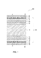
FIG. 1 is a cross sectional diagram showing a structure of a solar cell module according to a first preferred embodiment of the present invention. -
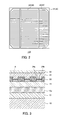
FIG. 2 is a plan view showing a structure of the solar cell module according to the first preferred embodiment of the present invention. -
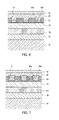
FIG. 3 is an enlarged cross sectional diagram showing a structure of the solar cell module according to the first preferred embodiment of the present invention. -
FIG. 4 is an enlarged cross sectional diagram showing another configuration of the structure of the solar cell module according to the first preferred embodiment of the present invention. -
FIG. 5 is a cross sectional diagram showing a structure of a solar cell module according to a second preferred embodiment of the present invention. -
FIG. 6 is an enlarged cross sectional diagram showing a structure of the solar cell according to the second preferred embodiment of the present invention. -
FIG. 7 is an enlarged cross sectional diagram showing another configuration of the structure of the solar cell module according to the second preferred embodiment of the present invention. - As shown in a cross sectional diagram of
FIG. 1 , asolar cell 100 according to a first preferred embodiment of the present invention comprises asubstrate 10, an i-typeamorphous layer 12i, a p-typeamorphous layer 12p, a transparentconductive layer 14, an i-typeamorphous layer 16i, an n-typeamorphous layer 16n, a transparentconductive layer 18,coating layers electrodes amorphous layer 12i, the p-typeamorphous layer 12p, the i-typeamorphous layer 16i, and the n-typeamorphous layer 16n may include crystal grains. In addition, asolar cell module 300 comprises thesolar cell 100,sealing layers members - A structure of the
solar cell 100 will now be described while a manufacturing method of thesolar cell 100 is described. - The
substrate 10 is a wafer-shaped plate made of a crystalline semiconductor material. Thesubstrate 10 may be a substrate made of a crystalline semiconductor of an n-type conductivity or a p-type conductivity. For thesubstrate 10, for example, a monocrystalline silicon substrate, a polycrystalline silicon substrate, a gallium arsenide substrate (GaAs), an indium phosphide substrate (InP), or the like may be employed. Thesubstrate 10 absorbs incident light and produces carrier pairs of electrons and holes by a photoelectric conversion effect. In the following, an example configuration will be described which uses a substrate made of n-type monocrystalline silicon as thesubstrate 10. - First, a pre-process such as cleaning is applied on the
substrate 10. In the pre-process, a projection-and-depression structure which is called a textured structure is formed on at least the light receiving surface of thesubstrate 10. - The i-type
amorphous layer 12i is, for example, an intrinsic amorphous silicon semiconductor layer formed over one primary surface of thesubstrate 10. The i-typeamorphous layer 12i may contain hydrogen. The p-typeamorphous layer 12p is formed over the i-typeamorphous layer 12i. The p-typeamorphous layer 12p is, for example, a p-type amorphous silicon semiconductor layer. The p-typeamorphous layer 12p may contain hydrogen. - The i-type
amorphous layer 12i is inserted between the p-typeamorphous layer 12p and thesubstrate 10 in order to improve a contact characteristic between the p-typeamorphous layer 12p and thesubstrate 10. Because of this, a thickness of the i-typeamorphous layer 12i is set to a thickness which would substantially not contribute to power generation, for example, in a range of greater than or equal to 0.1 nm and less than or equal to 25 nm, and more preferably, in a range of greater than or equal to 5 nm and less than or equal to 10 nm. - The i-type
amorphous layer 12i and the p-typeamorphous layer 12p may be formed through film formation methods such as CVD, such as plasma chemical vapor deposition or sputtering. - The i-type
amorphous layer 16i is, for example, an intrinsic amorphous silicon semiconductor layer formed over the other primary surface of thesubstrate 10. The i-typeamorphous layer 16i may contain hydrogen. The n-typeamorphous layer 16n is formed over the i-typeamorphous layer 16i. For example, the n-typeamorphous layer 16n is an n-type amorphous silicon semiconductor layer. The n-typeamorphous layer 16n may contain hydrogen. - The i-type
amorphous layer 16i is inserted between the n-typeamorphous layer 16n and thesubstrate 10 in order to improve a contact characteristic between the n-typeamorphous layer 16n and thesubstrate 10. Because of this, similar to the i-typeamorphous layer 12i, a thickness of the i-typeamorphous layer 16i is set to a thickness which would substantially not contribute to the power generation, for example, in a range of greater than or equal to 0.1 nm and less than or equal to 25 nm, more preferably, in a range of greater than or equal to 5 nm and less than or equal to 10 nm. - The i-type
amorphous layer 16i and the n-typeamorphous layer 16n can be formed through film formation methods such as CVD, sputtering, or the like. - The transparent
conductive layer 14 is formed over the p-typeamorphous layer 12p, and the transparentconductive layer 18 is formed over the n-typeamorphous layer 16n. The transparentconductive layers conductive layers conductive layers conductive layers - The
coating layer 20 is formed over the transparentconductive layer 14, and thecoating layer 22 is formed over the transparentconductive layer 18. Thecoating layers electrodes coating layers coating layers coating layers - The
coating layers conductive layers coating layers coating layers FIG. 2 , the coating layers 20 and 22 are formed in a pattern having an opening A (refer toFIG. 1 ) corresponding to the shapes of the collectingelectrodes conductive layers - The collecting
electrode 24 is a conductive layer over the transparentconductive layer 14, and the collectingelectrode 26 is a conductive layer over the transparentconductive layer 18. The collecting layers 24 and 26 preferably have an comb-shaped structure including a plurality of finger portions and a bus bar portion connecting the plurality of finger portions, so that the electric power generated by thesolar cell 100 can be evenly collected. - The collecting electrode will now be descried exemplifying the collecting
electrode 24. As shown in an enlarged cross sectional diagram ofFIG. 3 , the collectingelectrode 24 has a multilayer structure including a primaryconductive layer 24a and anovercoat layer 24b. The primaryconductive layer 24a is a metal layer having a primary composition of copper, in consideration of the high conductivity, the ease of machining, and the price of the material. Theovercoat layer 24b is an overcoating layer of the primaryconductive layer 24a, and is placed between the primaryconductive layer 24a and thesealing layer 28 to be described later. Theovercoat layer 24b is a metal layer including at least one of nickel (Ni), tin (Sn), titanium (Ti), tantalum (Ta), tungsten (W), and palladium (Pd). It is sufficient that theovercoat layer 24b cover at least a part of the primaryconductive layer 24a so that the primaryconductive layer 24a does not directly contact thesealing layer 28, but theovercoat layer 24b preferably covers the entire primaryconductive layer 24a. - A thickness of the primary
conductive layer 24a may be determined according to a width of the collectingelectrode 24 and necessary conductivity, and is preferably set, for example, to about a few tens of µm. A thickness of theovercoat layer 24b is preferably set in a range of greater than or equal to 0.2 µm and less than or equal to 10 µm according to a diffusion characteristic of copper among the materials forming theovercoat layer 24b. For example, because nickel has a smaller diffusion coefficient with respect to copper, when theovercoat layer 24b is formed using nickel, the thickness may be set to be greater than or equal to 0.2 µm, and when theovercoat layer 24b is formed with tin, the thickness is preferably set to be greater than or equal to 5 µm. - The collecting
electrode 24 is embedded in the opening A of thecoating layer 20. A thickness of the collectingelectrode 24 may be set thinner than the thickness of thecoating layer 20 as shown inFIG. 3 , or may be set thicker than the thickness of thecoating layer 20 as shown inFIG. 4 . By setting the thickness of the collectingelectrode 24 to be thinner than the thickness of thecoating layer 20, a depression formed by an upper surface of the collectingelectrode 24 and side surfaces of thecoating layer 20 is formed in the opening A. Thesealing layer 28 then enters the depression of the opening A. Because of this, even when thesealing layer 28 is thermally expanded during the use, the thermal expansion of thesealing layer 28 is inhibited by the side surfaces of the opening A of thecoating layer 20. As a result, a close-contact property of thecoating layer 20 and thesealing layer 28 can be improved, and the detachment of thecoating layer 20 and thesealing layer 28 can be inhibited. - In addition, a contact area between the collecting
electrode 24 and thesealing layer 28 is reduced, and thus the reliability of thesolar cell module 300 can be improved as will be described later. On the other hand, by setting the thickness of the collectingelectrode 24 to be thicker than the thickness of thecoating layer 20, it becomes possible to obtain necessary conductivity for the collectingelectrode 24 even when the width of the collectingelectrode 24 is narrowed, and consequently, an advantage can be obtained in that an effective area of light reception can be increased, or the like. - The formation method of the collecting
electrode 24 is not particularly limited, but the collectingelectrode 24 is preferably formed through electroplating. After the insulatingcoating layer 20 having the opening A is formed, a voltage is applied on the transparentconductive layer 14 and the collectingelectrode 24 is formed through electroplating. After the primaryconductive layer 24a is formed, theovercoat layer 24b is formed over the primaryconductive layer 24a. Thicknesses of the primaryconductive layer 24a and theovercoat layer 24b can be adjusted by conditions such as an applied voltage, a current value, a film formation duration, etc., during the electroplating. - The thicknesses of the
coating layer 20 and the collectingelectrode 24 can be checked by a cross-sectional observation using an electron microscope. For example, a relationship between the thicknesses of thecoating layer 20 and the collectingelectrode 24 can be identified using a cross sectional SEM or a cross sectional TEM. - The
solar cell 100 is sealed by the encapsulatingmember 32. Thesealing layer 28 is positioned over thecoating layer 20 and the collectingelectrode 24, and the encapsulatingmember 32 is pressed under a heated condition to seal thesolar cell 100. Thesealing layer 28 is preferably a resin such as ethylene vinyl acetate (EVA), polyvinyl butyrate (PVB). The encapsulating member on the side of the front surface (light receiving surface) of thesolar cell 100 is preferably a glass plate or a resin sheet having a light transmitting characteristic. For the encapsulating member on the side of the back surface of thesolar cell 100, in addition to the glass plate and resin sheet having light transmitting characteristic, a light blocking member such as a resin film formed by sandwiching a metal foil may be employed. Although not shown in the figures, thesolar cell module 300 includes a plurality ofsolar cells 100 electrically connected by wiring members. The wiring member is generally connected to the bus bar portion of the collecting electrode. - In this manner, with the
overcoat layer 24b covering the primaryconductive layer 24a, diffusion of copper contained in the primaryconductive layer 24a into thesealing layer 28 is inhibited, and color change and degradation of thesealing layer 28 can be prevented. Or, with theovercoat layer 24b, oxidation of copper contained in the primaryconductive layer 24a is inhibited, and color change and degradation of the primaryconductive layer 24a can be prevented. As a result of these measures, reliability of thesolar cell module 300 can be improved. - In the above description, the
coating layer 20, the collectingelectrode 24, thesealing layer 28, and the encapsulatingmember 32 are described. Thecoating layer 22, the collectingelectrode 26, thesealing layer 30, and the encapsulatingmember 34 on the opposite side may have similar structures. However, when the above-described structure is employed in at least a part of one of the sides, the advantage can be obtained to a certain degree. - As shown in a cross sectional diagram of
FIG. 5 , asolar cell 200 according to a second preferred embodiment of the present invention comprises thesubstrate 10, the i-typeamorphous layer 12i, the p-typeamorphous layer 12p, the transparentconductive layer 14, the i-typeamorphous layer 16i, the n-typeamorphous layer 16n, the transparentconductive layer 18, the coating layers 20 and 22, and collectingelectrodes solar cell module 400 includes thesolar cell 200, the sealing layers 28 and 30, and the encapsulatingmembers - The
solar cell 200 has a similar structure to that of thesolar cell 100 in the first preferred embodiment of the present invention except that the structures of the collectingelectrodes electrodes - In the following, the collecting electrodes will be described exemplifying the collecting
electrode 36. As shown in an enlarged cross sectional diagram ofFIG. 6 , the collectingelectrode 36 has a multilayer structure of anundercoat layer 36a and a primaryconductive layer 36b. The collectingelectrode 36 is embedded in an opening B of thecoating layer 20. Theundercoat layer 36a is an undercoating layer of the primaryconductive layer 36b, and is provided between the transparentconductive layer 14 and the primaryconductive layer 36b so that the primaryconductive layer 36b does not directly contact the transparentconductive layer 14. The primaryconductive layer 36b is provided over theundercoat layer 36a. Theundercoat layer 36a is a metal layer including at least one of nickel, tin, titanium, tantalum, tungsten, and palladium. The primaryconductive layer 36b is a metal layer having a primary composition of copper (Cu). A thickness of theundercoat layer 36a may be preferably set in a range of greater than or equal to 0.2 µm and less than or equal to 10 µm, according to the materials forming theundercoat layer 36a. For example, because nickel has a smaller diffusion coefficient with respect to copper, when theundercoat layer 36a is formed with nickel, the thickness may be set to be greater than or equal to 0.2 µm, and when theundercoat layer 36a is formed with tin, the thickness is preferably set to be greater than or equal to 5 µm. A thickness of the primaryconductive layer 36b is preferably set to be about a few tens of µm. A thickness of the collectingelectrode 36 may be set to be thinner than the thickness of thecoating layer 20 as shown inFIG. 6 or thicker than the thickness of thecoating layer 20 as shown inFIG. 7 . - The collecting
electrode 36 is preferably formed through electroplating. After an insulatingcoating layer 20 having an opening B is formed, a voltage is applied to the transparentconductive layer 14, and theundercoat layer 36a is formed through electroplating. Then, the primaryconductive layer 36b is formed over theundercoat layer 36a. The thicknesses of theundercoat layer 36a and the primaryconductive layer 36b can be adjusted by conditions such as an applied voltage, a current value, and a film formation duration, etc., during the electroplating. - In this manner, by providing the
undercoat layer 36a between the semiconductor which is a photoelectric conversion region and the primaryconductive layer 36b, diffusion of copper contained in the primaryconductive layer 36b to the semiconductor can be inhibited, and reduction in the power generation characteristic can be inhibited. As a result, reliability of thesolar cell module 400 can be improved. In the above description, the collectingelectrode 36 has been described. The collectingelectrode 38 on the opposite side may be similarly formed. However, when the above-described structure is employed in at least a part of one of the sides, the advantage can be obtained to a certain degree. - Alternatively, the structure according to the first preferred embodiment of the present invention and the structure according to the second preferred embodiment of the present invention may be combined. In other words, the collecting electrode may be formed in a layered structure of the undercoat layer, primary conductive layer, and overcoat layer. In addition, the overcoat layer or the undercoat layer may have a layered structure of a plurality of materials.
- Moreover, for the overcoat layer or the undercoat layer, an epoxy-based resin or the like may be employed. In this case, the overcoat layer or the undercoat layer may be formed by applying the resin through screen printing, inkjet printing, or the like. In addition, when a resin is used for the overcoat layer or the undercoat layer, an opening for electrically connecting the primary conductive layer and other conductive members may become necessary in the overcoat layer or the undercoat layer.
- Moreover, the application of the present invention is not limited to a crystalline solar cell, and the present invention may be similarly applied to other types of thin film solar cells so long as the solar cell has the collecting electrode.
- 10 SUBSTRATE; 12i i-TYPE AMORPHOUS LAYER; 12p p-TYPE AMORPHOUS LAYER; 14 TRANSPARENT CONDUCTIVE LAYER; 16i i-TYPE AMORPHOUS LAYER; 16n n-TYPE AMORPHOUS LAYER; 18 TRANSPARENT CONDUCTIVE LAYER; 20, 22 COATING LAYER; 24, 26 COLLECTING ELECTRODE; 24a PRIMARY CONDUCTIVE LAYER; 24b OVERCOAT LAYER; 28, 30 SEALING LAYER; 32, 34 ENCAPSULATING MEMBER; 36, 38 COLLECTING ELECTRODE; 36a UNDERCOAT LAYER; 36b PRIMARY CONDUCTIVE LAYER; 100, 200 SOLAR CELL; 300, 400 SOLAR CELL MODULE
Claims (6)
- A solar cell in which a collecting electrode is formed on at least one of a light receiving surface and a back surface, wherein
the collecting electrode comprises a primary conductive layer including copper, and at least one of an overcoat layer covering an upper surface side of the primary conductive layer and an undercoat layer covering a lower surface side of the primary conductive layer. - The solar cell according to Claim 1, wherein
the overcoat layer or the undercoat layer is a metal layer including at least one of nickel, tin, titanium, tantalum, tungsten, and palladium. - The solar cell according to Claim 1, wherein
the overcoat layer or the undercoat layer is a resin layer. - The solar cell according to any one of Claims 1 - 3, wherein
the collecting electrode is formed between insulating coating layers, and
a thickness of the collecting electrode is lower than a thickness of the coating layer. - A solar cell module having the solar cell according to any one of Claims 1 - 4, comprising
a sealing layer of a resin covering an upper surface side of the collecting electrode. - A method of manufacturing a solar cell, comprising:a first step of forming a coating layer having an opening over at least one of a light receiving surface and a back surface;a second step of plating the one surface which is exposed in the opening with a metal, to thereby form a collecting electrode having a lower thickness than that of the coating layer; anda third step of covering the coating layer and the collecting electrode with a sealing layer, whereinthe second step comprises a step of forming a primary conductive layer including copper, and a step of forming at least one of an overcoat layer covering an upper surface side of the primary conductive layer and an undercoat layer covering a lower surface side of the primary conductive layer.
Applications Claiming Priority (1)
| Application Number | Priority Date | Filing Date | Title |
|---|---|---|---|
| PCT/JP2011/072325 WO2013046386A1 (en) | 2011-09-29 | 2011-09-29 | Solar cell, solar cell module, and method for manufacturing solar cell |
Publications (3)
| Publication Number | Publication Date |
|---|---|
| EP2763185A1 true EP2763185A1 (en) | 2014-08-06 |
| EP2763185A4 EP2763185A4 (en) | 2015-04-29 |
| EP2763185B1 EP2763185B1 (en) | 2021-09-01 |
Family
ID=47994493
Family Applications (1)
| Application Number | Title | Priority Date | Filing Date |
|---|---|---|---|
| EP11873077.9A Active EP2763185B1 (en) | 2011-09-29 | 2011-09-29 | Solar cell module |
Country Status (4)
| Country | Link |
|---|---|
| US (2) | US9502589B2 (en) |
| EP (1) | EP2763185B1 (en) |
| JP (1) | JP5935047B2 (en) |
| WO (1) | WO2013046386A1 (en) |
Families Citing this family (1)
| Publication number | Priority date | Publication date | Assignee | Title |
|---|---|---|---|---|
| JP6184263B2 (en) * | 2013-09-11 | 2017-08-23 | 三菱電機株式会社 | Manufacturing method of solar cell module |
Family Cites Families (21)
| Publication number | Priority date | Publication date | Assignee | Title |
|---|---|---|---|---|
| JPH036867A (en) * | 1989-06-05 | 1991-01-14 | Mitsubishi Electric Corp | Electrode structure of photovoltaic device, forming method, and apparatus for manufacture thereof |
| JPH03250671A (en) * | 1990-01-31 | 1991-11-08 | Sharp Corp | Semiconductor photoelectric converting device and its manufacture |
| JPH04146684A (en) | 1990-10-08 | 1992-05-20 | Matsushita Electric Ind Co Ltd | Circuit board and manufacture thereof |
| JP2938634B2 (en) * | 1991-10-08 | 1999-08-23 | キヤノン株式会社 | Solar cell module |
| US5543333A (en) * | 1993-09-30 | 1996-08-06 | Siemens Solar Gmbh | Method for manufacturing a solar cell having combined metallization |
| AUPP437598A0 (en) * | 1998-06-29 | 1998-07-23 | Unisearch Limited | A self aligning method for forming a selective emitter and metallization in a solar cell |
| JP2000058885A (en) | 1998-08-03 | 2000-02-25 | Sanyo Electric Co Ltd | Solar cell and method of manufacturing the same |
| JP3937945B2 (en) * | 2002-07-04 | 2007-06-27 | セイコーエプソン株式会社 | Display device and electronic apparatus equipped with the same |
| JP2004247596A (en) * | 2003-02-14 | 2004-09-02 | Kyocera Corp | Solar cell element, method of manufacturing the same, and solar cell module using the solar cell element |
| EP1608719A2 (en) * | 2003-03-05 | 2005-12-28 | Electrochromix, Inc | Electrochromic mirrors and other electrooptic devices |
| US20070240759A1 (en) * | 2006-04-13 | 2007-10-18 | Applied Materials, Inc. | Stacked thin film photovoltaic module and method for making same using IC processing |
| JP2008135654A (en) * | 2006-11-29 | 2008-06-12 | Sanyo Electric Co Ltd | Solar cell module |
| JP4817254B2 (en) * | 2006-12-01 | 2011-11-16 | 大日本塗料株式会社 | Zirconium oxide particle dispersion, photocurable composition containing zirconium oxide particles, and cured film |
| US20090139868A1 (en) | 2007-12-03 | 2009-06-04 | Palo Alto Research Center Incorporated | Method of Forming Conductive Lines and Similar Features |
| US20090223549A1 (en) * | 2008-03-10 | 2009-09-10 | Calisolar, Inc. | solar cell and fabrication method using crystalline silicon based on lower grade feedstock materials |
| US7833808B2 (en) * | 2008-03-24 | 2010-11-16 | Palo Alto Research Center Incorporated | Methods for forming multiple-layer electrode structures for silicon photovoltaic cells |
| JP2011171270A (en) * | 2010-01-25 | 2011-09-01 | Hitachi Chem Co Ltd | Paste composition for electrode, and solar cell |
| JP5535709B2 (en) * | 2010-03-19 | 2014-07-02 | 三洋電機株式会社 | SOLAR CELL, SOLAR CELL MODULE USING THE SOLAR CELL, AND SOLAR CELL MANUFACTURING METHOD |
| KR101661768B1 (en) * | 2010-09-03 | 2016-09-30 | 엘지전자 주식회사 | Solar cell and manufacturing method thereof |
| KR101699300B1 (en) * | 2010-09-27 | 2017-01-24 | 엘지전자 주식회사 | Solar cell and manufacturing method thereof |
| US20120222736A1 (en) * | 2011-03-04 | 2012-09-06 | Applied Materials, Inc. | Front contact solar cell manufacture using metal paste metallization |
-
2011
- 2011-09-29 EP EP11873077.9A patent/EP2763185B1/en active Active
- 2011-09-29 JP JP2013535734A patent/JP5935047B2/en active Active
- 2011-09-29 WO PCT/JP2011/072325 patent/WO2013046386A1/en not_active Ceased
-
2014
- 2014-02-28 US US14/193,638 patent/US9502589B2/en active Active
-
2016
- 2016-10-20 US US15/298,753 patent/US9972728B2/en active Active
Also Published As
| Publication number | Publication date |
|---|---|
| WO2013046386A1 (en) | 2013-04-04 |
| EP2763185A4 (en) | 2015-04-29 |
| US20140174531A1 (en) | 2014-06-26 |
| US9972728B2 (en) | 2018-05-15 |
| EP2763185B1 (en) | 2021-09-01 |
| JPWO2013046386A1 (en) | 2015-03-26 |
| JP5935047B2 (en) | 2016-06-15 |
| US20170040468A1 (en) | 2017-02-09 |
| US9502589B2 (en) | 2016-11-22 |
Similar Documents
| Publication | Publication Date | Title |
|---|---|---|
| EP2930755B1 (en) | Solar cell and method for manufacturing the same | |
| EP2092571B1 (en) | Front electrode with thin metal film layer and high work-function buffer layer for use in photovoltaic device and method of making same | |
| EP2428997B1 (en) | Solar cell with electroplated metal grid | |
| EP3496158A1 (en) | Solar cell and method of manufacturing the same | |
| US10453981B2 (en) | Solar cell, solar cell module, method for manufacturing solar cell, and method for manufacturing solar cell module | |
| EP3136451B1 (en) | Crystalline-silicon solar cell, crystalline-silicon solar-cell module, and manufacturing methods therefor | |
| EP2434548B1 (en) | Solar cell and method for manufacturing the same | |
| US20200091362A1 (en) | Solar cell module and method for producing same | |
| EP3474333B1 (en) | Solar cell and production method therefor, and solar cell module | |
| US20140069479A1 (en) | Photoelectric Device Module and Manufacturing Method Thereof | |
| WO2016001828A1 (en) | Solar cell | |
| US20120006391A1 (en) | Photovoltaic module and method of manufacturing a photovoltaic module having an electrode diffusion layer | |
| US9786809B2 (en) | Method of forming electrode pattern and method of manufacturing solar cell | |
| US9972728B2 (en) | Solar cell, solar cell module, and method for manufacturing solar cell | |
| US20190305151A1 (en) | Solar cell and manufacturing method of the same | |
| WO2012105153A1 (en) | Photoelectric conversion element | |
| WO2012090650A1 (en) | Solar cell | |
| JP6191995B2 (en) | Solar cell module | |
| US20150207019A1 (en) | Method for Fabricating Crystalline Silicon Solar Cell Having Passivation Layer and Local Rear Contacts | |
| US10930810B2 (en) | Solar cell and method of manufacturing solar cell | |
| JP2004260013A (en) | Photoelectric conversion device and manufacturing method thereof | |
| WO2013128566A1 (en) | Solar cell and method for manufacturing same | |
| WO2013042242A1 (en) | Solar cell, solar cell module, and methods for manufacturing solar cell and solar cell module |
Legal Events
| Date | Code | Title | Description |
|---|---|---|---|
| PUAI | Public reference made under article 153(3) epc to a published international application that has entered the european phase |
Free format text: ORIGINAL CODE: 0009012 |
|
| 17P | Request for examination filed |
Effective date: 20140221 |
|
| AK | Designated contracting states |
Kind code of ref document: A1 Designated state(s): AL AT BE BG CH CY CZ DE DK EE ES FI FR GB GR HR HU IE IS IT LI LT LU LV MC MK MT NL NO PL PT RO RS SE SI SK SM TR |
|
| DAX | Request for extension of the european patent (deleted) | ||
| RA4 | Supplementary search report drawn up and despatched (corrected) |
Effective date: 20150327 |
|
| RIC1 | Information provided on ipc code assigned before grant |
Ipc: H01L 31/0747 20120101ALI20150323BHEP Ipc: H01L 31/048 20140101ALI20150323BHEP Ipc: H01L 31/0224 20060101AFI20150323BHEP |
|
| RAP1 | Party data changed (applicant data changed or rights of an application transferred) |
Owner name: PANASONIC INTELLECTUAL PROPERTY MANAGEMENT CO., LT |
|
| STAA | Information on the status of an ep patent application or granted ep patent |
Free format text: STATUS: EXAMINATION IS IN PROGRESS |
|
| 17Q | First examination report despatched |
Effective date: 20191105 |
|
| GRAP | Despatch of communication of intention to grant a patent |
Free format text: ORIGINAL CODE: EPIDOSNIGR1 |
|
| STAA | Information on the status of an ep patent application or granted ep patent |
Free format text: STATUS: GRANT OF PATENT IS INTENDED |
|
| INTG | Intention to grant announced |
Effective date: 20210331 |
|
| GRAS | Grant fee paid |
Free format text: ORIGINAL CODE: EPIDOSNIGR3 |
|
| GRAA | (expected) grant |
Free format text: ORIGINAL CODE: 0009210 |
|
| STAA | Information on the status of an ep patent application or granted ep patent |
Free format text: STATUS: THE PATENT HAS BEEN GRANTED |
|
| AK | Designated contracting states |
Kind code of ref document: B1 Designated state(s): AL AT BE BG CH CY CZ DE DK EE ES FI FR GB GR HR HU IE IS IT LI LT LU LV MC MK MT NL NO PL PT RO RS SE SI SK SM TR |
|
| REG | Reference to a national code |
Ref country code: GB Ref legal event code: FG4D |
|
| REG | Reference to a national code |
Ref country code: CH Ref legal event code: EP Ref country code: AT Ref legal event code: REF Ref document number: 1427132 Country of ref document: AT Kind code of ref document: T Effective date: 20210915 |
|
| REG | Reference to a national code |
Ref country code: DE Ref legal event code: R096 Ref document number: 602011071708 Country of ref document: DE |
|
| REG | Reference to a national code |
Ref country code: IE Ref legal event code: FG4D |
|
| REG | Reference to a national code |
Ref country code: LT Ref legal event code: MG9D |
|
| REG | Reference to a national code |
Ref country code: NL Ref legal event code: MP Effective date: 20210901 |
|
| PG25 | Lapsed in a contracting state [announced via postgrant information from national office to epo] |
Ref country code: SE Free format text: LAPSE BECAUSE OF FAILURE TO SUBMIT A TRANSLATION OF THE DESCRIPTION OR TO PAY THE FEE WITHIN THE PRESCRIBED TIME-LIMIT Effective date: 20210901 Ref country code: HR Free format text: LAPSE BECAUSE OF FAILURE TO SUBMIT A TRANSLATION OF THE DESCRIPTION OR TO PAY THE FEE WITHIN THE PRESCRIBED TIME-LIMIT Effective date: 20210901 Ref country code: BG Free format text: LAPSE BECAUSE OF FAILURE TO SUBMIT A TRANSLATION OF THE DESCRIPTION OR TO PAY THE FEE WITHIN THE PRESCRIBED TIME-LIMIT Effective date: 20211201 Ref country code: LT Free format text: LAPSE BECAUSE OF FAILURE TO SUBMIT A TRANSLATION OF THE DESCRIPTION OR TO PAY THE FEE WITHIN THE PRESCRIBED TIME-LIMIT Effective date: 20210901 Ref country code: NO Free format text: LAPSE BECAUSE OF FAILURE TO SUBMIT A TRANSLATION OF THE DESCRIPTION OR TO PAY THE FEE WITHIN THE PRESCRIBED TIME-LIMIT Effective date: 20211201 Ref country code: RS Free format text: LAPSE BECAUSE OF FAILURE TO SUBMIT A TRANSLATION OF THE DESCRIPTION OR TO PAY THE FEE WITHIN THE PRESCRIBED TIME-LIMIT Effective date: 20210901 Ref country code: FI Free format text: LAPSE BECAUSE OF FAILURE TO SUBMIT A TRANSLATION OF THE DESCRIPTION OR TO PAY THE FEE WITHIN THE PRESCRIBED TIME-LIMIT Effective date: 20210901 Ref country code: ES Free format text: LAPSE BECAUSE OF FAILURE TO SUBMIT A TRANSLATION OF THE DESCRIPTION OR TO PAY THE FEE WITHIN THE PRESCRIBED TIME-LIMIT Effective date: 20210901 |
|
| REG | Reference to a national code |
Ref country code: AT Ref legal event code: MK05 Ref document number: 1427132 Country of ref document: AT Kind code of ref document: T Effective date: 20210901 |
|
| PG25 | Lapsed in a contracting state [announced via postgrant information from national office to epo] |
Ref country code: PL Free format text: LAPSE BECAUSE OF FAILURE TO SUBMIT A TRANSLATION OF THE DESCRIPTION OR TO PAY THE FEE WITHIN THE PRESCRIBED TIME-LIMIT Effective date: 20210901 Ref country code: LV Free format text: LAPSE BECAUSE OF FAILURE TO SUBMIT A TRANSLATION OF THE DESCRIPTION OR TO PAY THE FEE WITHIN THE PRESCRIBED TIME-LIMIT Effective date: 20210901 Ref country code: GR Free format text: LAPSE BECAUSE OF FAILURE TO SUBMIT A TRANSLATION OF THE DESCRIPTION OR TO PAY THE FEE WITHIN THE PRESCRIBED TIME-LIMIT Effective date: 20211202 |
|
| PG25 | Lapsed in a contracting state [announced via postgrant information from national office to epo] |
Ref country code: AT Free format text: LAPSE BECAUSE OF FAILURE TO SUBMIT A TRANSLATION OF THE DESCRIPTION OR TO PAY THE FEE WITHIN THE PRESCRIBED TIME-LIMIT Effective date: 20210901 |
|
| REG | Reference to a national code |
Ref country code: CH Ref legal event code: PL |
|
| REG | Reference to a national code |
Ref country code: BE Ref legal event code: MM Effective date: 20210930 |
|
| PG25 | Lapsed in a contracting state [announced via postgrant information from national office to epo] |
Ref country code: IS Free format text: LAPSE BECAUSE OF FAILURE TO SUBMIT A TRANSLATION OF THE DESCRIPTION OR TO PAY THE FEE WITHIN THE PRESCRIBED TIME-LIMIT Effective date: 20220101 Ref country code: SM Free format text: LAPSE BECAUSE OF FAILURE TO SUBMIT A TRANSLATION OF THE DESCRIPTION OR TO PAY THE FEE WITHIN THE PRESCRIBED TIME-LIMIT Effective date: 20210901 Ref country code: SK Free format text: LAPSE BECAUSE OF FAILURE TO SUBMIT A TRANSLATION OF THE DESCRIPTION OR TO PAY THE FEE WITHIN THE PRESCRIBED TIME-LIMIT Effective date: 20210901 Ref country code: RO Free format text: LAPSE BECAUSE OF FAILURE TO SUBMIT A TRANSLATION OF THE DESCRIPTION OR TO PAY THE FEE WITHIN THE PRESCRIBED TIME-LIMIT Effective date: 20210901 Ref country code: PT Free format text: LAPSE BECAUSE OF FAILURE TO SUBMIT A TRANSLATION OF THE DESCRIPTION OR TO PAY THE FEE WITHIN THE PRESCRIBED TIME-LIMIT Effective date: 20220103 Ref country code: NL Free format text: LAPSE BECAUSE OF FAILURE TO SUBMIT A TRANSLATION OF THE DESCRIPTION OR TO PAY THE FEE WITHIN THE PRESCRIBED TIME-LIMIT Effective date: 20210901 Ref country code: EE Free format text: LAPSE BECAUSE OF FAILURE TO SUBMIT A TRANSLATION OF THE DESCRIPTION OR TO PAY THE FEE WITHIN THE PRESCRIBED TIME-LIMIT Effective date: 20210901 Ref country code: CZ Free format text: LAPSE BECAUSE OF FAILURE TO SUBMIT A TRANSLATION OF THE DESCRIPTION OR TO PAY THE FEE WITHIN THE PRESCRIBED TIME-LIMIT Effective date: 20210901 Ref country code: AL Free format text: LAPSE BECAUSE OF FAILURE TO SUBMIT A TRANSLATION OF THE DESCRIPTION OR TO PAY THE FEE WITHIN THE PRESCRIBED TIME-LIMIT Effective date: 20210901 |
|
| REG | Reference to a national code |
Ref country code: DE Ref legal event code: R097 Ref document number: 602011071708 Country of ref document: DE |
|
| PG25 | Lapsed in a contracting state [announced via postgrant information from national office to epo] |
Ref country code: MC Free format text: LAPSE BECAUSE OF FAILURE TO SUBMIT A TRANSLATION OF THE DESCRIPTION OR TO PAY THE FEE WITHIN THE PRESCRIBED TIME-LIMIT Effective date: 20210901 |
|
| PLBE | No opposition filed within time limit |
Free format text: ORIGINAL CODE: 0009261 |
|
| STAA | Information on the status of an ep patent application or granted ep patent |
Free format text: STATUS: NO OPPOSITION FILED WITHIN TIME LIMIT |
|
| PG25 | Lapsed in a contracting state [announced via postgrant information from national office to epo] |
Ref country code: LU Free format text: LAPSE BECAUSE OF NON-PAYMENT OF DUE FEES Effective date: 20210929 Ref country code: IT Free format text: LAPSE BECAUSE OF FAILURE TO SUBMIT A TRANSLATION OF THE DESCRIPTION OR TO PAY THE FEE WITHIN THE PRESCRIBED TIME-LIMIT Effective date: 20210901 Ref country code: IE Free format text: LAPSE BECAUSE OF NON-PAYMENT OF DUE FEES Effective date: 20210929 Ref country code: DK Free format text: LAPSE BECAUSE OF FAILURE TO SUBMIT A TRANSLATION OF THE DESCRIPTION OR TO PAY THE FEE WITHIN THE PRESCRIBED TIME-LIMIT Effective date: 20210901 Ref country code: BE Free format text: LAPSE BECAUSE OF NON-PAYMENT OF DUE FEES Effective date: 20210930 |
|
| 26N | No opposition filed |
Effective date: 20220602 |
|
| GBPC | Gb: european patent ceased through non-payment of renewal fee |
Effective date: 20211201 |
|
| PG25 | Lapsed in a contracting state [announced via postgrant information from national office to epo] |
Ref country code: SI Free format text: LAPSE BECAUSE OF FAILURE TO SUBMIT A TRANSLATION OF THE DESCRIPTION OR TO PAY THE FEE WITHIN THE PRESCRIBED TIME-LIMIT Effective date: 20210901 Ref country code: LI Free format text: LAPSE BECAUSE OF NON-PAYMENT OF DUE FEES Effective date: 20210930 Ref country code: CH Free format text: LAPSE BECAUSE OF NON-PAYMENT OF DUE FEES Effective date: 20210930 |
|
| PG25 | Lapsed in a contracting state [announced via postgrant information from national office to epo] |
Ref country code: FR Free format text: LAPSE BECAUSE OF NON-PAYMENT OF DUE FEES Effective date: 20211101 |
|
| PG25 | Lapsed in a contracting state [announced via postgrant information from national office to epo] |
Ref country code: GB Free format text: LAPSE BECAUSE OF NON-PAYMENT OF DUE FEES Effective date: 20211201 |
|
| PG25 | Lapsed in a contracting state [announced via postgrant information from national office to epo] |
Ref country code: HU Free format text: LAPSE BECAUSE OF FAILURE TO SUBMIT A TRANSLATION OF THE DESCRIPTION OR TO PAY THE FEE WITHIN THE PRESCRIBED TIME-LIMIT; INVALID AB INITIO Effective date: 20110929 Ref country code: CY Free format text: LAPSE BECAUSE OF FAILURE TO SUBMIT A TRANSLATION OF THE DESCRIPTION OR TO PAY THE FEE WITHIN THE PRESCRIBED TIME-LIMIT Effective date: 20210901 |
|
| PG25 | Lapsed in a contracting state [announced via postgrant information from national office to epo] |
Ref country code: MK Free format text: LAPSE BECAUSE OF FAILURE TO SUBMIT A TRANSLATION OF THE DESCRIPTION OR TO PAY THE FEE WITHIN THE PRESCRIBED TIME-LIMIT Effective date: 20210901 |
|
| PG25 | Lapsed in a contracting state [announced via postgrant information from national office to epo] |
Ref country code: TR Free format text: LAPSE BECAUSE OF FAILURE TO SUBMIT A TRANSLATION OF THE DESCRIPTION OR TO PAY THE FEE WITHIN THE PRESCRIBED TIME-LIMIT Effective date: 20210901 |
|
| PG25 | Lapsed in a contracting state [announced via postgrant information from national office to epo] |
Ref country code: MT Free format text: LAPSE BECAUSE OF FAILURE TO SUBMIT A TRANSLATION OF THE DESCRIPTION OR TO PAY THE FEE WITHIN THE PRESCRIBED TIME-LIMIT Effective date: 20210901 |
|
| REG | Reference to a national code |
Ref country code: DE Ref legal event code: R079 Ref document number: 602011071708 Country of ref document: DE Free format text: PREVIOUS MAIN CLASS: H01L0031022400 Ipc: H10F0077200000 |
|
| PGFP | Annual fee paid to national office [announced via postgrant information from national office to epo] |
Ref country code: DE Payment date: 20250919 Year of fee payment: 15 |