EP2763138A2 - Ambient temperature wire bonding method, as well as the device obtained thereby - Google Patents
Ambient temperature wire bonding method, as well as the device obtained thereby Download PDFInfo
- Publication number
- EP2763138A2 EP2763138A2 EP14153507.0A EP14153507A EP2763138A2 EP 2763138 A2 EP2763138 A2 EP 2763138A2 EP 14153507 A EP14153507 A EP 14153507A EP 2763138 A2 EP2763138 A2 EP 2763138A2
- Authority
- EP
- European Patent Office
- Prior art keywords
- bonding
- ball
- gold alloy
- slider
- less
- Prior art date
- Legal status (The legal status is an assumption and is not a legal conclusion. Google has not performed a legal analysis and makes no representation as to the accuracy of the status listed.)
- Withdrawn
Links
Images




Classifications
-
- G—PHYSICS
- G11—INFORMATION STORAGE
- G11B—INFORMATION STORAGE BASED ON RELATIVE MOVEMENT BETWEEN RECORD CARRIER AND TRANSDUCER
- G11B5/00—Recording by magnetisation or demagnetisation of a record carrier; Reproducing by magnetic means; Record carriers therefor
- G11B5/48—Disposition or mounting of heads or head supports relative to record carriers ; arrangements of heads, e.g. for scanning the record carrier to increase the relative speed
-
- G—PHYSICS
- G11—INFORMATION STORAGE
- G11B—INFORMATION STORAGE BASED ON RELATIVE MOVEMENT BETWEEN RECORD CARRIER AND TRANSDUCER
- G11B5/00—Recording by magnetisation or demagnetisation of a record carrier; Reproducing by magnetic means; Record carriers therefor
- G11B5/10—Structure or manufacture of housings or shields for heads
- G11B5/102—Manufacture of housing
-
- B—PERFORMING OPERATIONS; TRANSPORTING
- B23—MACHINE TOOLS; METAL-WORKING NOT OTHERWISE PROVIDED FOR
- B23K—SOLDERING OR UNSOLDERING; WELDING; CLADDING OR PLATING BY SOLDERING OR WELDING; CUTTING BY APPLYING HEAT LOCALLY, e.g. FLAME CUTTING; WORKING BY LASER BEAM
- B23K20/00—Non-electric welding by applying impact or other pressure, with or without the application of heat, e.g. cladding or plating
- B23K20/10—Non-electric welding by applying impact or other pressure, with or without the application of heat, e.g. cladding or plating making use of vibrations, e.g. ultrasonic welding
-
- G—PHYSICS
- G11—INFORMATION STORAGE
- G11B—INFORMATION STORAGE BASED ON RELATIVE MOVEMENT BETWEEN RECORD CARRIER AND TRANSDUCER
- G11B5/00—Recording by magnetisation or demagnetisation of a record carrier; Reproducing by magnetic means; Record carriers therefor
- G11B5/127—Structure or manufacture of heads, e.g. inductive
- G11B5/31—Structure or manufacture of heads, e.g. inductive using thin films
- G11B5/3163—Fabrication methods or processes specially adapted for a particular head structure, e.g. using base layers for electroplating, using functional layers for masking, using energy or particle beams for shaping the structure or modifying the properties of the basic layers
- G11B5/3169—Working or finishing the interfacing surface of heads, e.g. lapping of heads
-
- G—PHYSICS
- G11—INFORMATION STORAGE
- G11B—INFORMATION STORAGE BASED ON RELATIVE MOVEMENT BETWEEN RECORD CARRIER AND TRANSDUCER
- G11B5/00—Recording by magnetisation or demagnetisation of a record carrier; Reproducing by magnetic means; Record carriers therefor
- G11B5/127—Structure or manufacture of heads, e.g. inductive
- G11B5/31—Structure or manufacture of heads, e.g. inductive using thin films
- G11B5/3163—Fabrication methods or processes specially adapted for a particular head structure, e.g. using base layers for electroplating, using functional layers for masking, using energy or particle beams for shaping the structure or modifying the properties of the basic layers
- G11B5/3173—Batch fabrication, i.e. producing a plurality of head structures in one batch
-
- G—PHYSICS
- G11—INFORMATION STORAGE
- G11B—INFORMATION STORAGE BASED ON RELATIVE MOVEMENT BETWEEN RECORD CARRIER AND TRANSDUCER
- G11B5/00—Recording by magnetisation or demagnetisation of a record carrier; Reproducing by magnetic means; Record carriers therefor
- G11B5/48—Disposition or mounting of heads or head supports relative to record carriers ; arrangements of heads, e.g. for scanning the record carrier to increase the relative speed
- G11B5/4806—Disposition or mounting of heads or head supports relative to record carriers ; arrangements of heads, e.g. for scanning the record carrier to increase the relative speed specially adapted for disk drive assemblies, e.g. assembly prior to operation, hard or flexible disk drives
- G11B5/4826—Mounting, aligning or attachment of the transducer head relative to the arm assembly, e.g. slider holding members, gimbals, adhesive
-
- G—PHYSICS
- G11—INFORMATION STORAGE
- G11B—INFORMATION STORAGE BASED ON RELATIVE MOVEMENT BETWEEN RECORD CARRIER AND TRANSDUCER
- G11B5/00—Recording by magnetisation or demagnetisation of a record carrier; Reproducing by magnetic means; Record carriers therefor
- G11B2005/0002—Special dispositions or recording techniques
- G11B2005/0005—Arrangements, methods or circuits
- G11B2005/0021—Thermally assisted recording using an auxiliary energy source for heating the recording layer locally to assist the magnetization reversal
-
- H—ELECTRICITY
- H10—SEMICONDUCTOR DEVICES; ELECTRIC SOLID-STATE DEVICES NOT OTHERWISE PROVIDED FOR
- H10W—GENERIC PACKAGES, INTERCONNECTIONS, CONNECTORS OR OTHER CONSTRUCTIONAL DETAILS OF DEVICES COVERED BY CLASS H10
- H10W72/00—Interconnections or connectors in packages
- H10W72/01—Manufacture or treatment
- H10W72/015—Manufacture or treatment of bond wires
- H10W72/01571—Cleaning, e.g. oxide removal or de-smearing
-
- H—ELECTRICITY
- H10—SEMICONDUCTOR DEVICES; ELECTRIC SOLID-STATE DEVICES NOT OTHERWISE PROVIDED FOR
- H10W—GENERIC PACKAGES, INTERCONNECTIONS, CONNECTORS OR OTHER CONSTRUCTIONAL DETAILS OF DEVICES COVERED BY CLASS H10
- H10W72/00—Interconnections or connectors in packages
- H10W72/071—Connecting or disconnecting
- H10W72/075—Connecting or disconnecting of bond wires
- H10W72/07511—Treating the bonding area before connecting, e.g. by applying flux or cleaning
-
- H—ELECTRICITY
- H10—SEMICONDUCTOR DEVICES; ELECTRIC SOLID-STATE DEVICES NOT OTHERWISE PROVIDED FOR
- H10W—GENERIC PACKAGES, INTERCONNECTIONS, CONNECTORS OR OTHER CONSTRUCTIONAL DETAILS OF DEVICES COVERED BY CLASS H10
- H10W72/00—Interconnections or connectors in packages
- H10W72/071—Connecting or disconnecting
- H10W72/075—Connecting or disconnecting of bond wires
- H10W72/07531—Techniques
- H10W72/07532—Compression bonding, e.g. thermocompression bonding
- H10W72/07533—Ultrasonic bonding, e.g. thermosonic bonding
-
- H—ELECTRICITY
- H10—SEMICONDUCTOR DEVICES; ELECTRIC SOLID-STATE DEVICES NOT OTHERWISE PROVIDED FOR
- H10W—GENERIC PACKAGES, INTERCONNECTIONS, CONNECTORS OR OTHER CONSTRUCTIONAL DETAILS OF DEVICES COVERED BY CLASS H10
- H10W72/00—Interconnections or connectors in packages
- H10W72/071—Connecting or disconnecting
- H10W72/075—Connecting or disconnecting of bond wires
- H10W72/07541—Controlling the environment, e.g. atmosphere composition or temperature
-
- H—ELECTRICITY
- H10—SEMICONDUCTOR DEVICES; ELECTRIC SOLID-STATE DEVICES NOT OTHERWISE PROVIDED FOR
- H10W—GENERIC PACKAGES, INTERCONNECTIONS, CONNECTORS OR OTHER CONSTRUCTIONAL DETAILS OF DEVICES COVERED BY CLASS H10
- H10W72/00—Interconnections or connectors in packages
- H10W72/50—Bond wires
- H10W72/531—Shapes of wire connectors
- H10W72/536—Shapes of wire connectors the connected ends being ball-shaped
-
- H—ELECTRICITY
- H10—SEMICONDUCTOR DEVICES; ELECTRIC SOLID-STATE DEVICES NOT OTHERWISE PROVIDED FOR
- H10W—GENERIC PACKAGES, INTERCONNECTIONS, CONNECTORS OR OTHER CONSTRUCTIONAL DETAILS OF DEVICES COVERED BY CLASS H10
- H10W72/00—Interconnections or connectors in packages
- H10W72/50—Bond wires
- H10W72/551—Materials of bond wires
- H10W72/552—Materials of bond wires comprising metals or metalloids, e.g. silver
-
- H—ELECTRICITY
- H10—SEMICONDUCTOR DEVICES; ELECTRIC SOLID-STATE DEVICES NOT OTHERWISE PROVIDED FOR
- H10W—GENERIC PACKAGES, INTERCONNECTIONS, CONNECTORS OR OTHER CONSTRUCTIONAL DETAILS OF DEVICES COVERED BY CLASS H10
- H10W72/00—Interconnections or connectors in packages
- H10W72/50—Bond wires
- H10W72/551—Materials of bond wires
- H10W72/552—Materials of bond wires comprising metals or metalloids, e.g. silver
- H10W72/5522—Materials of bond wires comprising metals or metalloids, e.g. silver comprising gold [Au]
-
- H—ELECTRICITY
- H10—SEMICONDUCTOR DEVICES; ELECTRIC SOLID-STATE DEVICES NOT OTHERWISE PROVIDED FOR
- H10W—GENERIC PACKAGES, INTERCONNECTIONS, CONNECTORS OR OTHER CONSTRUCTIONAL DETAILS OF DEVICES COVERED BY CLASS H10
- H10W72/00—Interconnections or connectors in packages
- H10W72/50—Bond wires
- H10W72/551—Materials of bond wires
- H10W72/552—Materials of bond wires comprising metals or metalloids, e.g. silver
- H10W72/5524—Materials of bond wires comprising metals or metalloids, e.g. silver comprising aluminium [Al]
-
- H—ELECTRICITY
- H10—SEMICONDUCTOR DEVICES; ELECTRIC SOLID-STATE DEVICES NOT OTHERWISE PROVIDED FOR
- H10W—GENERIC PACKAGES, INTERCONNECTIONS, CONNECTORS OR OTHER CONSTRUCTIONAL DETAILS OF DEVICES COVERED BY CLASS H10
- H10W72/00—Interconnections or connectors in packages
- H10W72/50—Bond wires
- H10W72/59—Bond pads specially adapted therefor
-
- H—ELECTRICITY
- H10—SEMICONDUCTOR DEVICES; ELECTRIC SOLID-STATE DEVICES NOT OTHERWISE PROVIDED FOR
- H10W—GENERIC PACKAGES, INTERCONNECTIONS, CONNECTORS OR OTHER CONSTRUCTIONAL DETAILS OF DEVICES COVERED BY CLASS H10
- H10W72/00—Interconnections or connectors in packages
- H10W72/90—Bond pads, in general
- H10W72/931—Shapes of bond pads
- H10W72/932—Plan-view shape, i.e. in top view
-
- H—ELECTRICITY
- H10—SEMICONDUCTOR DEVICES; ELECTRIC SOLID-STATE DEVICES NOT OTHERWISE PROVIDED FOR
- H10W—GENERIC PACKAGES, INTERCONNECTIONS, CONNECTORS OR OTHER CONSTRUCTIONAL DETAILS OF DEVICES COVERED BY CLASS H10
- H10W72/00—Interconnections or connectors in packages
- H10W72/90—Bond pads, in general
- H10W72/951—Materials of bond pads
- H10W72/952—Materials of bond pads comprising metals or metalloids, e.g. PbSn, Ag or Cu
Definitions
- Wire bonding is a method of making electrical interconnections among bonding pads, such as those located on an integrated circuit (IC) device and/or a printed circuit board (PCB) during semiconductor and/or storage device fabrication. Further, wire bonding can be used to connect an IC to other electronics or to connect from one PCB to another. Wire bonding is generally considered a cost-effective and flexible interconnect technology, which is used to assemble a wide variety of semiconductor packages. There are two main classes of wire bonding, wedge bonding and ball bonding. Both wedge bonding and ball bonding are typically accomplished using a combination of heat, compressive force, and ultrasonic energy to bond a wire to one or more bonding pads.
- Wedge bonding is typically carried out at room temperature, but has several limitations. First, the take-off angle and direction are substantially limited. Second, the wedge bond creates a relatively large foot size. Third, additional wedge bonds may not be stacked on top of a previous bonded spot on a bonding pad. As a result, wedge bonding is not an available options in applications with very small bonding pads or when an extruded object is in front of the take-off direction of the wedge bonded wire. Further, the bonded spot may not be reused due to oxidation (e.g., when an aluminum alloy wire is used), which could become a problem when the size of the bonding pad size is small and rewiring is necessary.
- oxidation e.g., when an aluminum alloy wire is used
- ball bonding typically heats the bonding pad to create the bond.
- heating the bonding pad may not be an available option due to the heat potentially damaging sensitive IC devices adjacent the bonding pad or other components of the IC (e.g., adhesives).
- Ball bonding has several advantages over the wedge bond, such as more flexibility in take-off direction and angle from the bonding pad without inducing unacceptable stresses on the bond, greatly reduced bonding size, and ball-on-ball stacking capability.
- a method comprising ball bonding a less than about 1 thousandth of an inch in diameter gold alloy wire to a gold alloy contact pad at about ambient temperature and using a ultrasonic bonding frequency greater than 60kHz and less than 200kHz.
- a method comprising:
- the gold alloy contact pad is less than about 1 micron thick.
- the gold alloy contact pad is not plasma cleaned prior to the ball bonding operation.
- the gold alloy wire is less than about 0.8 thousandths of an inch in diameter.
- the ultrasonic bonding frequency is about 120 kHz.
- the ambient temperature is between 15 degrees Celsius and 25 degrees Celsius.
- the method further comprises forming a gold ball at an end of the gold alloy wire, wherein the ball bonding operation bonds the gold ball to the gold alloy contact pad.
- a system comprising an electronic storage device slider having a less than 1 micron thick gold alloy contact pad with a less than 35 micron diameter gold alloy ball bond bonded to the gold alloy contact pad at about ambient temperature and using a ultrasonic bonding frequency greater than 60kHz and less than 200kHz.
- the gold alloy wire is less than about 1 thousandth of an inch in diameter.
- the ultrasonic bonding frequency is about 120 kHz.
- the ambient temperature is between 15 degrees Celsius and 25 degrees Celsius.
- the electronic storage device slider includes a protruding microelectronic component adjacent to the gold alloy contact pad.
- the ultrasonic bonding frequency is about 120 kHz.
- a planar bonding surface of the printed circuit board is oriented at about 5 degrees with respect to a planar bonding surface of the gold alloy contact pads.
- the system further comprises a planarization sensor with a resistance value that varies with a quantity of planarization performed on the bar of microelectronic devices.
- the printed circuit board is configured to monitor the resistance value of the planarization sensor to measure the quantity of planarization performed on the bar of microelectronic devices.
- each of two or more of the gold wires ball bonded to the microelectronic devices extend from the microelectronic devices at disparate angles.
- each of the microelectronic devices includes a protruding laser adjacent to one or more of the gold alloy contact pads.
- the microelectronic devices are electronic storage device sliders.
- FIG. 1 illustrates an example disc drive assembly 100 including a ball bond remnant 116 on a bonding pad 118 of a slider 120 (e.g., an AlTiC slider) located at a distal end of an actuator arm 110 and positioned over a storage media disc 108.
- the disc 108 includes an outer diameter 102 and an inner diameter 104, between which are a number of substantially circular data tracks (e.g., track 106) illustrated by circular dotted lines. In some implementations, there are more data tracks than illustrated in FIG. 1 .
- the disc 108 rotates at a high speed about a disc axis of rotation 112 as information is written to and read from the data tracks on the disc 108.
- the disc rotation speed may be fixed or variable.
- Information may be read from or written to the disc 108 through the use of read/write elements on the slider 120, which is located at a distal end of an actuator arm 110.
- the actuator arm 110 rotates about an actuator axis of rotation 114 during a seek operation to locate a desired data track and sector on the disc 108.
- Specific locations on the media disc 108 may be defined by any available addressing scheme (e.g., cylinder-head-sector (CHS) addressing and logical block addressing (LBA) schemes).
- CHS cylinder-head-sector
- LBA logical block addressing
- the actuator arm 110 extends toward the disc 108 and the slider 120 is located at the distal end of the actuator arm 110.
- the slider 120 flies in close proximity above the disc 108 while reading and writing data to the disc 108.
- a flex cable 122 provides the requisite electrical connection paths from a printed circuit board (PCB, not shown) to electronic components attached to the slider 120 (e.g., a read element and a write element), while allowing pivotal movement of the actuator arm 110 during operation.
- the flex cable 122 may be routed along the actuator arm 110 from the PCB to the slider 120.
- the PCB may include circuitry (e.g., a preamplifier (preamp)) for controlling the write currents applied to the write element during a write operation and amplifying read signals generated by the read element during a read operation).
- preamp preamplifier
- a side view of a trailing edge of the slider 120 is shown in detail in View B of the x-z plane of FIG. 1 .
- the slider 120 includes the bonding pad 118 (e.g., an electronic lapping guide (ELG) bonding pad with the ball bond remnant 116 attached thereto.
- the ball bond remnant 116 is a remnant from a wire previously ball bonded to the bonding pad 118.
- the ball bond remnant 116 is removed (e.g., by mechanically shaving it off of the bonding pad 118).
- the slider 120 may include additional bonding pads and ball bond remnants (not shown) behind the bonding pad 118 and the ball bond remnant 116 in the negative y-direction.
- the slider 120 may further include a microelectronic component 126 protruding from the slider 120 (e.g., a laser in a heat assisted magnetic recording (HAMR) device).
- a microelectronic component 126 protruding from the slider 120 e.g., a laser in a heat assisted magnetic recording (HAMR) device.
- the wire previously ball bonded to the bonding pad 118 is intentionally routed around the microelectronic component 126 to avoid contact with the protruding microelectronic component 126 as shown in detail in FIGs. 2 and 4 .
- the slider 120 may include additional microelectronic components (not shown) behind the microelectronic component 126 in the negative y-direction.
- the slider 120 further includes a planarization sensor 140 (also referred to as an "electronic lapping guide” or "ELG”) embedded within.
- the planarization sensor 140 electrically connects at least two bonding pads together within the slider 120.
- a cross-sectional area in the y-z plane of the planarization sensor 140 defines a resistive value of the planarization sensor 140 between the least two bonding pads.
- the slider 120 Prior to forming the air bearing surface (ABS) 130, the slider 120 is planarized (e.g., using lapping and/or chemical-mechanical polishing (CMP)), the y-z cross-sectional area of the planarization sensor 140 shrinks and its resistive value increases.
- CMP chemical-mechanical polishing
- the resistive value of the planarization sensor 140 can be measured and used to determine the amount of material removal on the ABS 130. As a result, planarization of the ABS 130 can be precisely controlled using the measured resistive value of the planarization sensor 140 and built-in actuators in a lapping carrier (not shown).
- An air-bearing 128 caused by aerodynamic forces is created between the ABS 130 of the slider 120 and a top surface of the disc 108 when the disc 108 is in motion.
- the ABS 130 of the slider 120 faces the disc 108 surface and is approximately parallel to the disc 108 surface (i.e., both are approximately in the x-y plane. As a result, no portion of the slider 120 substantially protrudes beyond the ABS 130 toward the disc 108 surface.
- An example process for creating this substantially smooth surface is described in detail with respect to FIGs. 2-5 below.
- the appearances of the slider 120 and other features of assembly 100 are for illustration purposes only and not drawn to scale. Further, the presently disclosed ball bonding technology may apply to storage drive assemblies other than the disc drive assembly 100 depicted in FIG. 1 . Still further, the presently disclosed technology may be used to ball bond wires to microelectronic devices other than sliders used in devices other than electronic storage devices.
- FIG. 2 illustrates a side view of an example lapping carrier assembly 200 that includes a slider row bar 232 ball bonded to a printed circuit board 234.
- the assembly 200 is used to obtain an accurately planarized and highly smooth (e.g., sub-nanometer variations) surface which will be patterned to form an air-bearing surface (ABS) (not shown, see FIGs. 1 , 4 , and 5 ).
- the row bar 232 includes a row of sliders (e.g., slider 124 of FIG. 1 ) for inclusion in a storage drive assembly (e.g., disc drive assembly 100 of FIG. 1 ), for example.
- the row bar 232 includes a row of microelectronic devices other than sliders.
- the row bar 232 is releasably bonded to a lapping carrier 236 using an adhesive 238 (e.g., a wafer grip or adhesive).
- the row bar 232 includes a microelectronic component 226 protruding from the row bar 232.
- the microelectronic component 226 is a laser in a heat assisted magnetic recording (HAMR) device.
- the row bar 232 further includes the bonding pad 218, which provides an electrical connection to a planarization sensor 240 embedded within the row bar 232.
- the planarization sensor 240 is discussed in more detail with reference to FIGs. 3 and 4 .
- the bonding pad 218 may be made of or coated with gold or metallic alloys.
- the bonding pad 218 is quite small (e.g., 127 ⁇ m x 85 ⁇ m or 50 ⁇ m x 50 ⁇ m square) and has a less than 1 micron thick (e.g., 0.25 microns thick) gold coating layer.
- the PCB 234 includes a PCB bonding pad 242, which provides an electrical connection to the PCB 234, which in turn may connect to to a lapping control unit that monitors and adjusts lapping operations on the row bar 232 in real time.
- the PCB 234 is connected to the row bar 232 via an electric trace 244 (or wire) connecting the bonding pads 218, 242.
- the trace 244 may be made of a gold or copper alloy.
- the PCB 234 may be mounted in any location and orientation with respect to the row bar 232 that is convenient.
- a planar bonding surface of the PCB bonding pad 242 is mounted at an angle (e.g., approximately 5 degrees) with respect to a planar bonding surface of the bonding pad 218 (e.g., the y-z plane) and is mounted to a top surface of the assembly 200 (not shown) via a strip of double-stick tape or a mechanical lock, for example.
- one end of the trace 244 is ball bonded to the bonding pad 218 (as depicted by ball bond 216).
- the ball bond is used in lieu of a wedge bond for several reasons.
- the takeoff angle of the wedge bond is limited to a relatively shallow angle from the bonding pad surface (e.g., less than 45 degrees) and a direction generally in the x-z plane (based on the orientation of a foot of the wedge bond).
- the bonding pad 218 Due to the proximity of the bonding pad 218 to the microelectronic component 226 protruding from the row bar 232 and the relative height in the negative x-direction of the microelectronic component 226 protruding from the row bar 232, such a shallow takeoff angle in a general direction of the PCB 234 may not be possible without colliding with the microelectronic component 226. Further, the foot of the wedge bond may be too large to accommodate the small size of the bonding pad 218 and/or the wedge bond may render the bonding pad 218 unusable for later electrical connections without additional processing of the bonding pad 218 surface.
- ball bonding typically requires heat to be applied to the bonding pad 218 to create a sufficiently strong bond to the trace 244.
- the temperature of the bonding pad 218 would exceed 125 degrees Celsius to form a sufficiently strong bond.
- This relatively high temperature may cause the adhesive 238 to melt or become soft, which could cause the row bar 232 to become loose or detached from the carrier 236, especially if and when any shear force is applied to the row bar 232 generally in the x-direction.
- thermal cycling the lapping carrier assembly 200 may alter the adhesive's mechanical properties and induce additional stress and strain to the assembly 200, which can deform the assembly 200 and negatively impact lapping performance.
- a ball bonding tool may apply ultrasonic energy (e.g., 120kHz) and compressive force (e.g., 0.2N using a 0.8mil diameter gold wire) to bond the trace 244 to the bonding pad 218 without heating the bonding pad 218.
- ultrasonic energy e.g., 120kHz
- compressive force e.g., 0.2N using a 0.8mil diameter gold wire
- a high ultrasonic frequency e.g., 120kHz over 60kHz
- properly scrubbing the bonding pad 218 to clean the bonding pad 218 enhances the energy transfer efficiency and interatomic movement during the bonding of the trace 244 to the pad 218.
- the trace 244 may be bonded to the pad 218 without applying any heat directly to the bonding pad 218.
- the trace 244 may be bonded to a relatively cool bonding pad 218 (e.g., at ambient or room temperature). More specifically, ambient temperature is referred to herein as ranging from about 15-25 degrees Celsius). In other implementations, the ball bonding process described herein may be performed successfully with the bonding pad 218 between 18-30 degrees Celsius or between 15-50 degrees Celsius.
- the ultrasonic frequency applied to form trace 244 is approximately 120kHz and the trace 244 is primarily gold with an approximately 0.7mil diameter. In other implementations, the ultrasonic frequency applied to the trace 244 ranges from above 60kHz to below 200kHz.
- An opposite end of the trace 244 is stitch bonded to the bonding pad 242.
- the trace 244 is ball bonded to the bonding pad 242 and stitch bonded to the bonding pad 218.
- the trace 244 diameter is less than about 1 thousandth of an inch in diameter of a gold alloy wire.
- the trace 244 may be less than about 1 thousandth of an inch in diameter in order to yield a ball bond with a size (e.g., cross-sectional area) significantly smaller than the contact pad 218 surface area.
- a size e.g., cross-sectional area
- a 0.7 thousandths of an inch trace may yield a ball bond approximately 33 ⁇ m in diameter on a 60 ⁇ mx60 ⁇ m contact pad.
- the trace 244 diameter becomes smaller, ball bonding the trace 244 to a contact pad without applying thermal energy rapidly becomes more difficult.
- the transfer of ultrasonic energy in ball bonding become less efficient with decreasing trace 244 diameter due to an increasing disparity between a fixed ultrasonic energy of the bonding tool (e.g., 120kHz) and the rapidly increasing resonant frequency associated with the ball at the end of the trace 244.
- the increasing resonant frequency is proportional to 1 m , where m represents the mass of the ball at the end of the trace 244. As the mass approaches zero, the resonant frequency approaches infinity.
- the trace 244 diameter decreases, the trace 244 is more susceptible to breaking, which renders the trace 244 increasingly difficult to handle and susceptible to breakage.
- the ultrasonic energy used to ball bond the trace 244 should match the resonant frequency of the trace 244 ball within an acceptable tolerance to maximize the energy transfer to the ball and pad 218. Applying the ultrasonic energy to the trace 244 becomes more difficult as the resonant frequency increases.
- the trace 244 resonant frequency is constrained such that a 200 kHz ultrasonic bonding frequency effectively works to create a ball bond without directly adding thermal energy at the bonding pad 218.
- a 120 kHz ultrasonic bonding frequency effectively works to ball bond a 0.7mil diameter trace without heating the trace.
- Other ultrasonic bonding frequencies are contemplated herein.
- FIG. 3 illustrates a top view of an example lapping carrier assembly 300 that includes a slider 324 in a row bar 332 with a pair of bonding pads 318, 319 ball bonded to a corresponding pair of bonding pads 342, 343 on a printed circuit board 334.
- the row bar 332 includes a row of sliders (e.g., the slider 324), each of which may be included in a storage drive assembly (e.g., disc drive assembly 100 of FIG. 1 ) or other electronic device.
- the row bar 332 includes a row of microelectronic devices other than sliders.
- the individual sliders may be separated by dicing the row bar 332 using dicing lanes (e.g., dicing lane 348).
- the depicted row bar 332 includes six separate sliders, although other implementations may include greater or fewer numbers of separate sliders.
- the row bar includes 62 separate functional sliders and two non-functional (or "dummy") sliders at each end of the row bar. While slider 324 is discussed with specificity with reference to FIG. 3 , any one or more of the other depicted sliders may be used in a similar manner.
- the row bar 332 is releasably bonded to a carrier 336 using an adhesive 338.
- the slider 324 includes a microelectronic component 326 protruding from the row bar 332 (in the negative x-direction).
- the microelectronic component 326 is a laser for use in a heat assisted magnetic recording (HAMR) device.
- the slider 324 further includes bonding pads (e.g., bonding pads 318, 319), each of which may provide an electrical connection to a planarization sensor (not shown) embedded within the slider 324.
- the slider 324 is depicted with two bonding pads for real-time in-situ monitoring and control of a lapping process, although other implementations may have greater or fewer numbers of bonding pads with varied functionality.
- the PCB 334 includes PCB bonding pads (e.g., PCB bonding pads 342, 343), each of which provides an electrical connection to the PCB 334 (e.g., to a lapping control unit (not shown) on or electrically connected to the PCB 334).
- the PCB 334 is depicted with 12 PCB bonding pads, although other implementations may have greater or fewer numbers of PCB bonding pads.
- the PCB 334 is connected to the slider 324 via electric traces or wires.
- bonding pad 318 is connected to PCB bonding pad 342 via electric trace 344 and bonding pad 319 is connected to PCB bonding pad 343 via electric trace 345.
- two electric traces are depicted, although other implementations may have greater or fewer numbers of electric traces.
- the PCB 334 may be mounted in any location and orientation with respect to the row bar 332 that is convenient.
- the slider 324 further includes a planarization sensor 340 embedded within (illustrated by dotted lines).
- the planarization sensor 340 electrically connects to the bonding pads 318, 319 on the slider 324.
- a cross-sectional area of the planarization sensor 340 is proportionally related to a resistive value of the planarization sensor 340.
- CMP chemical-mechanical polishing
- the cross-sectional area of the planarization sensor 340 decreases as its resistive value increases.
- a resistance value of the planarization sensor 340 correlates to the amount of material removal at the lapping surface of the slider 324. As a result, the slider 324 surface can be precisely planarized using the measured resistive value of the planarization sensor 340.
- the traces 344, 345 are ball bonded (see e.g., ball bond 316) to the bonding pads 318, 319, respectively.
- the ball bond is used in lieu of a wedge bond for several reasons.
- the takeoff angle of the wedge bond is limited to a relatively shallow angle from the bonding pad surface (e.g., less than 45 degrees) and a direction generally in the x-z plane (based on the orientation of a foot of the wedge bond).
- ball bonding typically requires heat to be applied to the bonding pad 318 to create a sufficiently strong bond to the trace 344.
- the temperature of the slider 324 would exceed 125 degrees Celsius to create a sufficiently strong bond. This high temperature may cause the adhesive 338 to melt or become soft, which may cause the row bar 332 to become loose or detached from the carrier 336, especially if and when any shear force is applied to the bonding pad 318 or other component of the row bar 332 generally in the x-direction.
- the thermally cycling the assembly 300 may alter the adhesive's mechanical properties and induce additional stress and strain to the assembly 300, which can deform the assembly 300 and negatively impact lapping performance and/or the output specifications for the row bar 332.
- a ball bonding tool may apply a relatively high frequency ultrasonic energy and compressive force with proper scrubbing of the bonding pad surfaces to bond the traces 344, 345 to the bonding pads 318, 319, respectively.
- the relatively high frequency ultrasonic signal reduces the energy gap between the ultrasonic frequency and the ball bond's resonant frequency, thereby enhancing the efficiency of ultrasonic energy transfer during bonding of the traces 344, 345 to the pads 318, 319.
- the traces 344, 345 may be bonded to the pads 318, 319 without applying any thermal energy directly to the bonding pads 318, 319 and while the bonding pads 318, 319 are generally maintained at room temperature with no thermal energy directly applied to the bonding pads 318, 319.
- each of the traces 344, 345 is stitch bonded to the PCB 334 at bonding pads 342, 343.
- the traces 344, 345 are ball bonded to the bonding pads 342, 343 and stitch bonded to the bonding pads 318, 319.
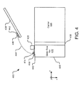
- FIG. 4 illustrates a side view of an example lapping carrier assembly 400 that includes a slider row bar 432 ball bonded to a printed circuit board 434 with an air-bearing surface 430 of the slider row bar 432 lapped co-planar with a planarization sensor 440 embedded within the slider row bar 432.
- the planarization assembly 400 is used to precisely lap the slider row bar 432 to obtain an accurately planarized and highly smooth air-bearing surface 430 of the row bar 432.
- the row bar 432 includes a row of sliders (e.g., slider 124 of FIG. 1 ) for inclusion in a storage drive assembly (e.g., disc drive assembly 100 of FIG. 1 ), for example.
- the row bar 432 includes a row of microelectronic devices other than sliders.
- the row bar 432 is releasably bonded to a carrier 436 using an adhesive 438.
- the row bar 432 includes microelectronic components (e.g., microelectronic component 426) protruding from the row bar 432.
- the microelectronic component 426 is a laser in a heat assisted magnetic recording (HAMR) device.
- the row bar 432 further includes bonding pads (e.g., bonding pad 418), which provide electrical connections to the row bar 432 (e.g., specifically to the planarization sensor 440).
- the row bar 432 further includes planarization sensors (e.g., planarization sensor 440 embedded within (illustrated by dotted lines). Each of the planarization sensors is electrically connected to a pair of bonding pads. For example, planarization sensor 440 is electrically connected to bonding pad 418 and a second bonding pad adjacent the bonding pad 418 (not shown) in the y-direction. A cross-sectional area (e.g., in the x-z plane) of the planarization sensor 440 defines a resistive value of the planarization sensor 440.
- planarization sensors e.g., planarization sensor 440 embedded within (illustrated by dotted lines).
- Each of the planarization sensors is electrically connected to a pair of bonding pads.
- planarization sensor 440 is electrically connected to bonding pad 418 and a second bonding pad adjacent the bonding pad 418 (not shown) in the y-direction.
- ABS air-bearing surface 430
- CMP chemical-mechanical polishing
- the x-z planar area of the planarization sensor 440 decreases and its resistive value increases (see planarization sensor 240 of FIG. 2 as compared to planarization sensor 440 of FIG. 4 .
- the resistive value of the planarization sensor 440 is a measurable quantity indicating the amount of planarization at the air-bearing surface 430.
- the air-bearing surface 430 can be precisely planarized using the measured resistive value of the planarization sensor 440 and built-in actuators in the lapping carrier 436.
- the PCB 434 includes PCB bonding pads (e.g., PCB bonding pad 442), which provide an electrical connections to the PCB 434 (e.g., to a lapping control unit (not shown).
- the PCB 434 is connected to the row bar 432 via electric traces or wires (e.g., electric trace 444) connecting the bonding pads.
- electric trace 444 connects bonding pads 418, 442.
- the PCB 434 may be mounted in any location and orientation with respect to the row bar 432 that is convenient.
- the trace 444 is ball bonded to the bonding pad 418 (as depicted by ball bond 416) and stitch bonded (as depicted by stitch bond 446) to the bonding pad 442.
- the trace 444 is ball bonded to the bonding pad 442 and stitch bonded to the bonding pad 418.
- FIG. 5 illustrates a side view of an example slider 524 with a ball bond remnant 516 attached thereto.
- the slider 524 includes a microelectronic component 526 protruding from the slider 524 in the negative x-direction.
- the microelectronic component 526 is a laser for a laser-in-slider (LIS) heat assisted magnetic recording (HAMR) technique.
- the slider 524 further includes a bonding pad 518, which provides an electrical connection to the slider 524, and a planarization sensor 540 embedded within the slider 524.
- LIS laser-in-slider
- HAMR heat assisted magnetic recording
- a slider row bar (not shown, see row bar 232, 332, 432 of FIGs. 2 , 3 , and 4 , respectively) is adequately lapped, a printed circuit board (not shown, see PCB 234, 334, 444 of FIGs. 2 , 3 , and 4 , respectively) and corresponding trace(s) (not shown, see trace 244, 344, 444 of FIGs. 2 , 3 , and 4 , respectively) from the slider row bar to the PCB are removed. Further, the slider row bar is diced, after ABS patterning operations, into individual sliders (e.g., slider 524) and used as sliders in a storage drive assembly (e.g., disc drive assembly 100 of FIG. 1 ), for example.
- a storage drive assembly e.g., disc drive assembly 100 of FIG. 1
- FIG. 6 illustrates a perspective view of an example lapping carrier assembly 600 that includes an example slider row bar 632 ball bonded to a printed circuit board 634.
- the row bar 632 includes a row of sliders (e.g., slider 624), each of which may be included in a storage drive assembly (e.g., disc drive assembly 100 of FIG. 1 ) or other electronic device.
- the row bar 632 includes a row of microelectronic devices other than sliders.
- the individual sliders may be separated by cutting up the row bar 632 using dicing lanes (e.g., dicing lane 648).
- the row bar 632 may be separated into four separate sliders using the dicing lanes, although other implementations may have greater or fewer numbers of separate sliders. While slider 624 is discussed with specificity with reference to FIG. 6 , any one or more of the other depicted sliders may be used in a similar manner.
- the row bar 632 is releasably bonded to a carrier 636 using an adhesive 638.
- the slider 624 includes a microelectronic component 626 protruding from the row bar 632 (in the negative x-direction).
- the microelectronic component 626 is a laser for a laser-in-slider (LIS) heat assisted magnetic recording (HAMR) device.
- the slider 624 further includes bonding pads (e.g., bonding pad 618).
- the slider 624 is depicted with six bonding pads, four of which provide an electrical connections to planarization sensors 640, 641 within the slider 624. Other implementations may have greater or fewer bonding pads, any number of which with electrical connections to the slider 624.
- planarization sensors 640, 641 embedded within the slider 624.
- Each of the planarization sensors 640, 641 are electrically connected to at least two of the bonding pads and may be used to monitor planarization operations on the row bar 632 (as described in detailed above).
- the PCB 634 includes PCB bonding pads (e.g., PCB bonding pad 642), each of which provides an electrical connection to the PCB 634 (e.g., to a lapping control unit (not shown)).
- PCB bonding pads e.g., PCB bonding pad 642
- the PCB 634 is connected to the slider 624 via electric traces or wires (e.g., electrical trace 644) connecting the bonding pads 618, 642.
- electrical trace 644 connecting the bonding pads 618, 642.
- four electrical traces are depicted, although other implementations may utilize a greater or fewer number of traces.
- the PCB 634 may be mounted in any location and orientation with respect to the row bar 632 that is convenient.
- the traces are ball bonded to the bonding pads on the slider 624 (as depicted by ball bond 616).
- the ball bond is used in lieu of a wedge bond for several reasons.
- the takeoff angle of the wedge bond is limited to a relatively shallow angle from the bonding pad surface (e.g., less than 45 degrees) and a direction generally in the x-z plane (based on the orientation of a foot of the wedge bond).
- the foot of the wedge bond may be too large to accommodate the small size of the slider 624 bonding pads and/or the wedge bond may render the slider 624 bonding pads unusable for later electrical connections without additional processing of the bonding pad surfaces.
- Ball bonding typically requires heat to be applied to the bonding pads to create a sufficiently strong bond to the traces.
- the temperature of the slider 624 would exceed 125 degrees Celsius to create a sufficiently strong bond.
- the high of a temperature may cause the adhesive 638 to melt or become soft, which would risk the row bar 632 becoming loose or detached from the carrier 636, especially if and when any shear force is applied to the bonding pad 618 or other component of the row bar 632 generally in the x-direction.
- the thermally cycling the assembly 600 may alter the adhesive's mechanical properties and induce additional stress and strain to the assembly 600, which can deform the assembly 600 and negatively impact lapping performance.
- a ball bonding tool may apply a relatively high frequency ultrasonic energy and compressive force with proper scrubbing on the bonding pad surfaces to clean the bonding pad surfaces to bond the traces to the bonding pads on the slider 624.
- the relatively high frequency ultrasonic signal enhances the efficiency of ultrasonic energy transfer during bonding of the traces to the bonding pads on the slider 624.
- the traces may be bonded to the bonding pads on the slider 624 without directly heating (e.g., applying thermal energy) to the bonding pads and while the bonding pads are generally at room temperature.
- each of the four depicted traces is stitch bonded to the bonding pads on the PCB 634 (as depicted by stitch bond 646).
- the traces are ball bonded to the bonding pads 642 on the PCB 634 and stitch bonded to the bonding pads on the slider 624.
- the ball bonds may each utilize a unique takeoff angle from the bonding pads on the slider 624 that allow the traces to extend to the PCB 634 without contacting one another.
- the flexible and unique takeoff angles allow the traces to extend between bonding pads with virtually any physical arrangement on the slider 624 and the PCB 634.
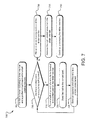
- FIG. 7 illustrates example operations 700 for using ball bonding to form wire interconnections between contact pads on a slider row bar and contact pads on a PCB without heating the contact pads on the slider row bar.
- Ball bonding is a type of wire bonding that may be used to make electrical interconnections as part of microelectronic device fabrication.
- a positioning operation 705 positions a carrier including a slider row bar and a printed circuit board within a ball bonding machine.
- the row bar includes a row of sliders, each of which has read and/or write heads and may be included in a storage drive assembly or other electronic device.
- the row bar may include contact pads (e.g., electronic lapping guide (ELG) pads) for providing electrical connections to the row bar (e.g., to planarization sensors within the row bar).
- EMG electronic lapping guide
- a decision operation 710 determines if there are unwired contact pads remaining to be ball bonded. If so, a forming operation 715 forms a ball at an end of a wire to be bonded to a contact pad on the slider row bar.
- the forming operation 715 may occur using an electric flame off (EFO) technique.
- EFO electric flame off
- a wire is fed through a needle-like disposable tool called a capillary of a bonding machine.
- a high-voltage electric arc applied near the wire tip, which melts the wire at the tip of the capillary.
- the tip of the wire forms into a ball because of the surface tension of the molten metal. After the electric arc is applied, the molten ball at the end of the wire quickly solidifies.
- a bonding operation 720 bonds the ball to the contact pad.
- the capillary is lowered to contact a surface of the bonding pad.
- the bonding machine applies ultrasonic energy and downward force that creates a bond between the ball and the bonding pad.
- the bonding pad may be plasma cleaned prior to the bonding operation 720. In other implementations, the bonding pad is not plasma cleaned.
- Bonding operation 725 bonds an opposite end of the wire to a printed circuit board (e.g., using a stitch bond or other available bonding techniques).
- Operations 710, 715, 720, 725 are repeated until there no remaining unwired contact pads to be ball bonded.
- the bonding operation 725 is performed after the operations 710, 715, 720 are complete.
- a planarization operation 730 planarizes an air-bearing surface of the slider row bar.
- the printed circuit board is used to connect the planarization sensors in the row bar and the lapping control unit, which detects a resistance change of the planarization sensors due to surface lapping.
- the lapping control unit uses this information to control built-in actuators in the lapping carrier to exert a desired quantity of pressure from the back of the slider row bar.
- one or more planarization sensors may be embedded within the row bar and are electrically connected to at least two of the bonding pads. A resistance value of the planarization sensors varies with the quantity of planarization applied to the row bar.
- a fixed current or voltage i.e., an excitation signal
- a corresponding the change in voltage or current i.e., an electric response
- This data may be fed back into the planarization operation 730 in order to achieve a desired planarization quantity. In this manner, the slider row bar may be precisely planarized.
- removing operation 735 breaks and removes the ball bonded wires running between the slider row bar and the PCB.
- the removing operation 735 is accomplished by applying a pulse air jet to blow away the interconnecting wires between the contacts pads on the slider row bar and the printed circuit board.
- the wires are mechanically sheared off from the slider row bar. Ball bond remnants may remain on some or all of the contact pads after the ball bonded wires are removed.
- a continuing operation 740 continues processing of the slider row bar for patterning of ABS and dicing the fully patterned row bar into individual sliders or other microelectronic components.
- additional processes steps are preformed to give the slider row bar desired characteristics and then the slider row bar is separated into individual sliders for use in an electronic storage device or other electronic device.
- dicing lanes are provided between neighboring sliders on the row bar that are used for dicing the row bar into the individual sliders. Further, the row bar is removed from the lapping carrier and placed onto a dicing carrier before being diced into the individual sliders.
Landscapes
- Engineering & Computer Science (AREA)
- Manufacturing & Machinery (AREA)
- Mechanical Engineering (AREA)
- Wire Bonding (AREA)
- Adjustment Of The Magnetic Head Position Track Following On Tapes (AREA)
Abstract
Description
- Wire bonding is a method of making electrical interconnections among bonding pads, such as those located on an integrated circuit (IC) device and/or a printed circuit board (PCB) during semiconductor and/or storage device fabrication. Further, wire bonding can be used to connect an IC to other electronics or to connect from one PCB to another. Wire bonding is generally considered a cost-effective and flexible interconnect technology, which is used to assemble a wide variety of semiconductor packages. There are two main classes of wire bonding, wedge bonding and ball bonding. Both wedge bonding and ball bonding are typically accomplished using a combination of heat, compressive force, and ultrasonic energy to bond a wire to one or more bonding pads.
- Wedge bonding is typically carried out at room temperature, but has several limitations. First, the take-off angle and direction are substantially limited. Second, the wedge bond creates a relatively large foot size. Third, additional wedge bonds may not be stacked on top of a previous bonded spot on a bonding pad. As a result, wedge bonding is not an available options in applications with very small bonding pads or when an extruded object is in front of the take-off direction of the wedge bonded wire. Further, the bonded spot may not be reused due to oxidation (e.g., when an aluminum alloy wire is used), which could become a problem when the size of the bonding pad size is small and rewiring is necessary.
- As distinct from wedge bonding, ball bonding typically heats the bonding pad to create the bond. However, heating the bonding pad may not be an available option due to the heat potentially damaging sensitive IC devices adjacent the bonding pad or other components of the IC (e.g., adhesives). Ball bonding has several advantages over the wedge bond, such as more flexibility in take-off direction and angle from the bonding pad without inducing unacceptable stresses on the bond, greatly reduced bonding size, and ball-on-ball stacking capability.
- A method comprising ball bonding a less than about 1 thousandth of an inch in diameter gold alloy wire to a gold alloy contact pad at about ambient temperature and using a ultrasonic bonding frequency greater than 60kHz and less than 200kHz.
- According to a first aspect of the present invention, there is provided a method comprising:
- ball bonding a less than about 1 thousandth of an inch in diameter gold alloy wire to a gold alloy contact pad at about ambient temperature and using a ultrasonic bonding frequency greater than 60kHz and less than 200kHz.
- Preferably, the gold alloy contact pad is less than about 1 micron thick.
- Preferably, the gold alloy contact pad is not plasma cleaned prior to the ball bonding operation.
- Preferably, the gold alloy wire is less than about 0.8 thousandths of an inch in diameter.
- Preferably, the ultrasonic bonding frequency is about 120 kHz.
- Preferably, the ambient temperature is between 15 degrees Celsius and 25 degrees Celsius.
- Preferably, the method further comprises forming a gold ball at an end of the gold alloy wire, wherein the ball bonding operation bonds the gold ball to the gold alloy contact pad.
- According to another aspect of the invention, there is provided a system comprising an electronic storage device slider having a less than 1 micron thick gold alloy contact pad with a less than 35 micron diameter gold alloy ball bond bonded to the gold alloy contact pad at about ambient temperature and using a ultrasonic bonding frequency greater than 60kHz and less than 200kHz.
- Preferably, the gold alloy wire is less than about 1 thousandth of an inch in diameter.
- Preferably, the ultrasonic bonding frequency is about 120 kHz.
- Preferably, the ambient temperature is between 15 degrees Celsius and 25 degrees Celsius.
- Preferably, the electronic storage device slider includes a protruding microelectronic component adjacent to the gold alloy contact pad.
- According to another aspect of the present invention, there is provided a system comprising:
- a printed circuit board with a less than about 1 thousandth of an inch diameter gold wire extending therefrom; and
- a bar of microelectronic devices, each with one or more less than 1 micron thick gold alloy contact pads, wherein the gold wires are ball bonded to the microelectronic devices at about ambient temperature and using a ultrasonic bonding frequency greater than 60kHz and less than 200kHz.
- Preferably, the ultrasonic bonding frequency is about 120 kHz.
- Preferably, a planar bonding surface of the printed circuit board is oriented at about 5 degrees with respect to a planar bonding surface of the gold alloy contact pads.
- Preferably, the system further comprises a planarization sensor with a resistance value that varies with a quantity of planarization performed on the bar of microelectronic devices.
- Preferably, the printed circuit board is configured to monitor the resistance value of the planarization sensor to measure the quantity of planarization performed on the bar of microelectronic devices.
- Preferably, each of two or more of the gold wires ball bonded to the microelectronic devices extend from the microelectronic devices at disparate angles.
- Preferably, each of the microelectronic devices includes a protruding laser adjacent to one or more of the gold alloy contact pads.
- Preferably, the microelectronic devices are electronic storage device sliders.
- Other implementations are also described and recited herein.
- Embodiments of the present invention will now be described by way of further example only and with reference to the accompanying drawings, in which:
-
FIG. 1 illustrates an example disc drive assembly including a ball bond remnant on a bonding pad of a slider located at a distal end of an actuator arm and positioned over a storage media disc. -
FIG. 2 illustrates a side view of an example lapping carrier assembly that includes a slider row bar ball bonded to a printed circuit board. -
FIG. 3 illustrates a top view of an example lapping carrier assembly that includes a slider row bar with one pair of bonding pads ball bonded to a corresponding pair of bonding pads on a printed circuit board. -
FIG. 4 illustrates a side view of an example lapping carrier assembly that includes a slider row bar ball bonded to a printed circuit board with an air-bearing surface of the slider row bar lapped co-planar with a planarization sensor embedded within the slider row bar. -
FIG. 5 illustrates a side view of an example slider row bar with a ball bond remnant attached thereto. -
FIG. 6 illustrates a perspective view of an example lapping carrier assembly that includes an example slider in a row bar ball bonded to a printed circuit board. -
FIG. 7 illustrates example operations for using ball bonding to form wire interconnections between contact pads on a slider row bar and contact pads on a PCB without heating the contact pads on the slider row bar. -
FIG. 1 illustrates an exampledisc drive assembly 100 including aball bond remnant 116 on abonding pad 118 of a slider 120 (e.g., an AlTiC slider) located at a distal end of anactuator arm 110 and positioned over astorage media disc 108. Referring specifically to View A (x-y plane), thedisc 108 includes anouter diameter 102 and aninner diameter 104, between which are a number of substantially circular data tracks (e.g., track 106) illustrated by circular dotted lines. In some implementations, there are more data tracks than illustrated inFIG. 1 . Thedisc 108 rotates at a high speed about a disc axis ofrotation 112 as information is written to and read from the data tracks on thedisc 108. The disc rotation speed may be fixed or variable. - Information may be read from or written to the
disc 108 through the use of read/write elements on theslider 120, which is located at a distal end of anactuator arm 110. Theactuator arm 110 rotates about an actuator axis ofrotation 114 during a seek operation to locate a desired data track and sector on thedisc 108. Specific locations on themedia disc 108 may be defined by any available addressing scheme (e.g., cylinder-head-sector (CHS) addressing and logical block addressing (LBA) schemes). Theactuator arm 110 extends toward thedisc 108 and theslider 120 is located at the distal end of theactuator arm 110. Theslider 120 flies in close proximity above thedisc 108 while reading and writing data to thedisc 108. In other implementations, there is more than oneslider 120,actuator arm 110, and/ordisc 108 in thedisc drive assembly 100. - A
flex cable 122 provides the requisite electrical connection paths from a printed circuit board (PCB, not shown) to electronic components attached to the slider 120 (e.g., a read element and a write element), while allowing pivotal movement of theactuator arm 110 during operation. Theflex cable 122 may be routed along theactuator arm 110 from the PCB to theslider 120. The PCB may include circuitry (e.g., a preamplifier (preamp)) for controlling the write currents applied to the write element during a write operation and amplifying read signals generated by the read element during a read operation). - A side view of a trailing edge of the
slider 120 is shown in detail in View B of the x-z plane ofFIG. 1 . Theslider 120 includes the bonding pad 118 (e.g., an electronic lapping guide (ELG) bonding pad with theball bond remnant 116 attached thereto. Theball bond remnant 116 is a remnant from a wire previously ball bonded to thebonding pad 118. In some implementations, theball bond remnant 116 is removed (e.g., by mechanically shaving it off of the bonding pad 118). Further, theslider 120 may include additional bonding pads and ball bond remnants (not shown) behind thebonding pad 118 and theball bond remnant 116 in the negative y-direction. - The
slider 120 may further include amicroelectronic component 126 protruding from the slider 120 (e.g., a laser in a heat assisted magnetic recording (HAMR) device). In one implementation, the wire previously ball bonded to thebonding pad 118 is intentionally routed around themicroelectronic component 126 to avoid contact with the protrudingmicroelectronic component 126 as shown in detail inFIGs. 2 and4 . Further, theslider 120 may include additional microelectronic components (not shown) behind themicroelectronic component 126 in the negative y-direction. - The
slider 120 further includes a planarization sensor 140 (also referred to as an "electronic lapping guide" or "ELG") embedded within. Theplanarization sensor 140 electrically connects at least two bonding pads together within theslider 120. A cross-sectional area in the y-z plane of theplanarization sensor 140 defines a resistive value of theplanarization sensor 140 between the least two bonding pads. Prior to forming the air bearing surface (ABS) 130, theslider 120 is planarized (e.g., using lapping and/or chemical-mechanical polishing (CMP)), the y-z cross-sectional area of theplanarization sensor 140 shrinks and its resistive value increases. The resistive value of theplanarization sensor 140 can be measured and used to determine the amount of material removal on theABS 130. As a result, planarization of theABS 130 can be precisely controlled using the measured resistive value of theplanarization sensor 140 and built-in actuators in a lapping carrier (not shown). - An air-
bearing 128 caused by aerodynamic forces is created between theABS 130 of theslider 120 and a top surface of thedisc 108 when thedisc 108 is in motion. TheABS 130 of theslider 120 faces thedisc 108 surface and is approximately parallel to thedisc 108 surface (i.e., both are approximately in the x-y plane. As a result, no portion of theslider 120 substantially protrudes beyond theABS 130 toward thedisc 108 surface. An example process for creating this substantially smooth surface is described in detail with respect toFIGs. 2-5 below. - The appearances of the
slider 120 and other features ofassembly 100 are for illustration purposes only and not drawn to scale. Further, the presently disclosed ball bonding technology may apply to storage drive assemblies other than thedisc drive assembly 100 depicted inFIG. 1 . Still further, the presently disclosed technology may be used to ball bond wires to microelectronic devices other than sliders used in devices other than electronic storage devices. -
FIG. 2 illustrates a side view of an examplelapping carrier assembly 200 that includes aslider row bar 232 ball bonded to a printedcircuit board 234. Theassembly 200 is used to obtain an accurately planarized and highly smooth (e.g., sub-nanometer variations) surface which will be patterned to form an air-bearing surface (ABS) (not shown, seeFIGs. 1 ,4 , and5 ). Therow bar 232 includes a row of sliders (e.g., slider 124 ofFIG. 1 ) for inclusion in a storage drive assembly (e.g.,disc drive assembly 100 ofFIG. 1 ), for example. In other implementations, therow bar 232 includes a row of microelectronic devices other than sliders. - The
row bar 232 is releasably bonded to alapping carrier 236 using an adhesive 238 (e.g., a wafer grip or adhesive). Therow bar 232 includes amicroelectronic component 226 protruding from therow bar 232. In one implementation, themicroelectronic component 226 is a laser in a heat assisted magnetic recording (HAMR) device. Therow bar 232 further includes thebonding pad 218, which provides an electrical connection to aplanarization sensor 240 embedded within therow bar 232. Theplanarization sensor 240 is discussed in more detail with reference toFIGs. 3 and4 . In various implementations, thebonding pad 218 may be made of or coated with gold or metallic alloys. In one implementation, thebonding pad 218 is quite small (e.g., 127µm x 85µm or 50µm x 50µm square) and has a less than 1 micron thick (e.g., 0.25 microns thick) gold coating layer. - The
PCB 234 includes aPCB bonding pad 242, which provides an electrical connection to thePCB 234, which in turn may connect to to a lapping control unit that monitors and adjusts lapping operations on therow bar 232 in real time. ThePCB 234 is connected to therow bar 232 via an electric trace 244 (or wire) connecting thebonding pads trace 244 may be made of a gold or copper alloy. ThePCB 234 may be mounted in any location and orientation with respect to therow bar 232 that is convenient. In one example implementation, a planar bonding surface of thePCB bonding pad 242 is mounted at an angle (e.g., approximately 5 degrees) with respect to a planar bonding surface of the bonding pad 218 (e.g., the y-z plane) and is mounted to a top surface of the assembly 200 (not shown) via a strip of double-stick tape or a mechanical lock, for example. - In this implementation, one end of the
trace 244 is ball bonded to the bonding pad 218 (as depicted by ball bond 216). The ball bond is used in lieu of a wedge bond for several reasons. One, the takeoff angle of the wedge bond is limited to a relatively shallow angle from the bonding pad surface (e.g., less than 45 degrees) and a direction generally in the x-z plane (based on the orientation of a foot of the wedge bond). Due to the proximity of thebonding pad 218 to themicroelectronic component 226 protruding from therow bar 232 and the relative height in the negative x-direction of themicroelectronic component 226 protruding from therow bar 232, such a shallow takeoff angle in a general direction of thePCB 234 may not be possible without colliding with themicroelectronic component 226. Further, the foot of the wedge bond may be too large to accommodate the small size of thebonding pad 218 and/or the wedge bond may render thebonding pad 218 unusable for later electrical connections without additional processing of thebonding pad 218 surface. - However, ball bonding typically requires heat to be applied to the
bonding pad 218 to create a sufficiently strong bond to thetrace 244. In many implementations, the temperature of thebonding pad 218 would exceed 125 degrees Celsius to form a sufficiently strong bond. This relatively high temperature may cause the adhesive 238 to melt or become soft, which could cause therow bar 232 to become loose or detached from thecarrier 236, especially if and when any shear force is applied to therow bar 232 generally in the x-direction. In addition, thermal cycling the lappingcarrier assembly 200 may alter the adhesive's mechanical properties and induce additional stress and strain to theassembly 200, which can deform theassembly 200 and negatively impact lapping performance. - In order to ball bond without thermally cycling the
assembly 200, a ball bonding tool (not shown) may apply ultrasonic energy (e.g., 120kHz) and compressive force (e.g., 0.2N using a 0.8mil diameter gold wire) to bond thetrace 244 to thebonding pad 218 without heating thebonding pad 218. Utilizing a high ultrasonic frequency (e.g., 120kHz over 60kHz) and properly scrubbing thebonding pad 218 to clean thebonding pad 218 enhances the energy transfer efficiency and interatomic movement during the bonding of thetrace 244 to thepad 218. As a result, thetrace 244 may be bonded to thepad 218 without applying any heat directly to thebonding pad 218. In other words, thetrace 244 may be bonded to a relatively cool bonding pad 218 (e.g., at ambient or room temperature). More specifically, ambient temperature is referred to herein as ranging from about 15-25 degrees Celsius). In other implementations, the ball bonding process described herein may be performed successfully with thebonding pad 218 between 18-30 degrees Celsius or between 15-50 degrees Celsius. In an example implementation, the ultrasonic frequency applied to formtrace 244 is approximately 120kHz and thetrace 244 is primarily gold with an approximately 0.7mil diameter. In other implementations, the ultrasonic frequency applied to thetrace 244 ranges from above 60kHz to below 200kHz. - An opposite end of the
trace 244 is stitch bonded to thebonding pad 242. In other implementations, thetrace 244 is ball bonded to thebonding pad 242 and stitch bonded to thebonding pad 218. - In one implementation, the
trace 244 diameter is less than about 1 thousandth of an inch in diameter of a gold alloy wire. Thetrace 244 may be less than about 1 thousandth of an inch in diameter in order to yield a ball bond with a size (e.g., cross-sectional area) significantly smaller than thecontact pad 218 surface area. For example, a 0.7 thousandths of an inch trace may yield a ball bond approximately 33µm in diameter on a 60µmx60µm contact pad. As thetrace 244 diameter becomes smaller, ball bonding thetrace 244 to a contact pad without applying thermal energy rapidly becomes more difficult. - First, the transfer of ultrasonic energy in ball bonding become less efficient with decreasing
trace 244 diameter due to an increasing disparity between a fixed ultrasonic energy of the bonding tool (e.g., 120kHz) and the rapidly increasing resonant frequency associated with the ball at the end of thetrace 244. The increasing resonant frequency is proportional to
trace 244. As the mass approaches zero, the resonant frequency approaches infinity. Second, as thetrace 244 diameter decreases, thetrace 244 is more susceptible to breaking, which renders thetrace 244 increasingly difficult to handle and susceptible to breakage. Even with 0.5mil diameter gold wire, thetrace 244 becomes extremely fragile and is therefore extremely difficult to perform consistent ball bonding using such a small diameter wire. As a result, ball bonding atrace 244 less than about 1mil (e.g., 0.7mil) in diameter is far less efficient in energy transfer and therefore much more challenging than ball bonding a trace between 1mil and 2mil, or greater, in diameter. - Further, as discussed above, the ultrasonic energy used to ball bond the
trace 244 should match the resonant frequency of thetrace 244 ball within an acceptable tolerance to maximize the energy transfer to the ball andpad 218. Applying the ultrasonic energy to thetrace 244 becomes more difficult as the resonant frequency increases. In one example implementation, thetrace 244 resonant frequency is constrained such that a 200 kHz ultrasonic bonding frequency effectively works to create a ball bond without directly adding thermal energy at thebonding pad 218. In other implementations, a 120 kHz ultrasonic bonding frequency effectively works to ball bond a 0.7mil diameter trace without heating the trace. Other ultrasonic bonding frequencies are contemplated herein. -
FIG. 3 illustrates a top view of an examplelapping carrier assembly 300 that includes aslider 324 in arow bar 332 with a pair ofbonding pads bonding pads circuit board 334. Therow bar 332 includes a row of sliders (e.g., the slider 324), each of which may be included in a storage drive assembly (e.g.,disc drive assembly 100 ofFIG. 1 ) or other electronic device. In other implementations, therow bar 332 includes a row of microelectronic devices other than sliders. - After ABS patterning, the individual sliders may be separated by dicing the
row bar 332 using dicing lanes (e.g., dicing lane 348). The depictedrow bar 332 includes six separate sliders, although other implementations may include greater or fewer numbers of separate sliders. In one example implementation, the row bar includes 62 separate functional sliders and two non-functional (or "dummy") sliders at each end of the row bar. Whileslider 324 is discussed with specificity with reference toFIG. 3 , any one or more of the other depicted sliders may be used in a similar manner. - The
row bar 332 is releasably bonded to acarrier 336 using an adhesive 338. Theslider 324 includes amicroelectronic component 326 protruding from the row bar 332 (in the negative x-direction). In one implementation, themicroelectronic component 326 is a laser for use in a heat assisted magnetic recording (HAMR) device. Theslider 324 further includes bonding pads (e.g.,bonding pads 318, 319), each of which may provide an electrical connection to a planarization sensor (not shown) embedded within theslider 324. Here, theslider 324 is depicted with two bonding pads for real-time in-situ monitoring and control of a lapping process, although other implementations may have greater or fewer numbers of bonding pads with varied functionality. - The
PCB 334 includes PCB bonding pads (e.g.,PCB bonding pads 342, 343), each of which provides an electrical connection to the PCB 334 (e.g., to a lapping control unit (not shown) on or electrically connected to the PCB 334). Here, thePCB 334 is depicted with 12 PCB bonding pads, although other implementations may have greater or fewer numbers of PCB bonding pads. ThePCB 334 is connected to theslider 324 via electric traces or wires. For example,bonding pad 318 is connected toPCB bonding pad 342 viaelectric trace 344 andbonding pad 319 is connected toPCB bonding pad 343 viaelectric trace 345. Here, two electric traces are depicted, although other implementations may have greater or fewer numbers of electric traces. ThePCB 334 may be mounted in any location and orientation with respect to therow bar 332 that is convenient. - The
slider 324 further includes a planarization sensor 340 embedded within (illustrated by dotted lines). The planarization sensor 340 electrically connects to thebonding pads slider 324. A cross-sectional area of the planarization sensor 340 is proportionally related to a resistive value of the planarization sensor 340. As theslider 324 is planarized (e.g., using lapping and/or chemical-mechanical polishing (CMP)), the cross-sectional area of the planarization sensor 340 decreases as its resistive value increases. A resistance value of the planarization sensor 340 correlates to the amount of material removal at the lapping surface of theslider 324. As a result, theslider 324 surface can be precisely planarized using the measured resistive value of the planarization sensor 340. - In this implementation, the
traces bonding pads bonding pads microelectronic component 326 protruding from therow bar 332 and the relative height in the negative x-direction of themicroelectronic component 326 protruding from therow bar 332, such a shallow takeoff angle in a general direction of thePCB 334 may not be possible without colliding with themicroelectronic component 326. Further, the foot of the wedge bond may be too large to accommodate the small size of thebonding pad 318 and/or the wedge bond may render thebonding pad 318 unusable for later electrical connections without additional processing of thebonding pad 318 surface. - However, ball bonding typically requires heat to be applied to the
bonding pad 318 to create a sufficiently strong bond to thetrace 344. In many implementations, the temperature of theslider 324 would exceed 125 degrees Celsius to create a sufficiently strong bond. This high temperature may cause the adhesive 338 to melt or become soft, which may cause therow bar 332 to become loose or detached from thecarrier 336, especially if and when any shear force is applied to thebonding pad 318 or other component of therow bar 332 generally in the x-direction. In addition, the thermally cycling theassembly 300 may alter the adhesive's mechanical properties and induce additional stress and strain to theassembly 300, which can deform theassembly 300 and negatively impact lapping performance and/or the output specifications for therow bar 332. - In order to ball bond without thermally cycling the
assembly 300, a ball bonding tool (not shown) may apply a relatively high frequency ultrasonic energy and compressive force with proper scrubbing of the bonding pad surfaces to bond thetraces bonding pads traces pads traces pads bonding pads bonding pads bonding pads - An opposite end of each of the
traces PCB 334 atbonding pads traces bonding pads bonding pads -
FIG. 4 illustrates a side view of an examplelapping carrier assembly 400 that includes aslider row bar 432 ball bonded to a printedcircuit board 434 with an air-bearingsurface 430 of theslider row bar 432 lapped co-planar with aplanarization sensor 440 embedded within theslider row bar 432. Theplanarization assembly 400 is used to precisely lap theslider row bar 432 to obtain an accurately planarized and highly smooth air-bearingsurface 430 of therow bar 432. Therow bar 432 includes a row of sliders (e.g., slider 124 ofFIG. 1 ) for inclusion in a storage drive assembly (e.g.,disc drive assembly 100 ofFIG. 1 ), for example. In other implementations, therow bar 432 includes a row of microelectronic devices other than sliders. - The
row bar 432 is releasably bonded to acarrier 436 using an adhesive 438. Therow bar 432 includes microelectronic components (e.g., microelectronic component 426) protruding from therow bar 432. In one implementation, themicroelectronic component 426 is a laser in a heat assisted magnetic recording (HAMR) device. Therow bar 432 further includes bonding pads (e.g., bonding pad 418), which provide electrical connections to the row bar 432 (e.g., specifically to the planarization sensor 440). - The
row bar 432 further includes planarization sensors (e.g.,planarization sensor 440 embedded within (illustrated by dotted lines). Each of the planarization sensors is electrically connected to a pair of bonding pads. For example,planarization sensor 440 is electrically connected tobonding pad 418 and a second bonding pad adjacent the bonding pad 418 (not shown) in the y-direction. A cross-sectional area (e.g., in the x-z plane) of theplanarization sensor 440 defines a resistive value of theplanarization sensor 440. As an air-bearing surface 430 (ABS) is planarized (e.g., using mechanical and/or chemical-mechanical polishing (CMP)), the x-z planar area of theplanarization sensor 440 decreases and its resistive value increases (seeplanarization sensor 240 ofFIG. 2 as compared toplanarization sensor 440 ofFIG. 4 . The resistive value of theplanarization sensor 440 is a measurable quantity indicating the amount of planarization at the air-bearingsurface 430. As a result, the air-bearingsurface 430 can be precisely planarized using the measured resistive value of theplanarization sensor 440 and built-in actuators in thelapping carrier 436. - The
PCB 434 includes PCB bonding pads (e.g., PCB bonding pad 442), which provide an electrical connections to the PCB 434 (e.g., to a lapping control unit (not shown). ThePCB 434 is connected to therow bar 432 via electric traces or wires (e.g., electric trace 444) connecting the bonding pads. For example,electric trace 444 connectsbonding pads PCB 434 may be mounted in any location and orientation with respect to therow bar 432 that is convenient. In this implementation, thetrace 444 is ball bonded to the bonding pad 418 (as depicted by ball bond 416) and stitch bonded (as depicted by stitch bond 446) to thebonding pad 442. In other implementations, thetrace 444 is ball bonded to thebonding pad 442 and stitch bonded to thebonding pad 418. -
FIG. 5 illustrates a side view of anexample slider 524 with aball bond remnant 516 attached thereto. Theslider 524 includes amicroelectronic component 526 protruding from theslider 524 in the negative x-direction. In one implementation, themicroelectronic component 526 is a laser for a laser-in-slider (LIS) heat assisted magnetic recording (HAMR) technique. Theslider 524 further includes abonding pad 518, which provides an electrical connection to theslider 524, and aplanarization sensor 540 embedded within theslider 524. - After an air-bearing
surface 530 of a slider row bar (not shown, seerow bar FIGs. 2 ,3 , and4 , respectively) is adequately lapped, a printed circuit board (not shown, seePCB FIGs. 2 ,3 , and4 , respectively) and corresponding trace(s) (not shown, seetrace FIGs. 2 ,3 , and4 , respectively) from the slider row bar to the PCB are removed. Further, the slider row bar is diced, after ABS patterning operations, into individual sliders (e.g., slider 524) and used as sliders in a storage drive assembly (e.g.,disc drive assembly 100 ofFIG. 1 ), for example. -
FIG. 6 illustrates a perspective view of an examplelapping carrier assembly 600 that includes an exampleslider row bar 632 ball bonded to a printedcircuit board 634. Therow bar 632 includes a row of sliders (e.g., slider 624), each of which may be included in a storage drive assembly (e.g.,disc drive assembly 100 ofFIG. 1 ) or other electronic device. In other implementations, therow bar 632 includes a row of microelectronic devices other than sliders. After the ABS is fully patterned, the individual sliders may be separated by cutting up therow bar 632 using dicing lanes (e.g., dicing lane 648). Here, therow bar 632 may be separated into four separate sliders using the dicing lanes, although other implementations may have greater or fewer numbers of separate sliders. Whileslider 624 is discussed with specificity with reference toFIG. 6 , any one or more of the other depicted sliders may be used in a similar manner. - The
row bar 632 is releasably bonded to acarrier 636 using an adhesive 638. Theslider 624 includes amicroelectronic component 626 protruding from the row bar 632 (in the negative x-direction). In one implementation, themicroelectronic component 626 is a laser for a laser-in-slider (LIS) heat assisted magnetic recording (HAMR) device. Theslider 624 further includes bonding pads (e.g., bonding pad 618). Here, theslider 624 is depicted with six bonding pads, four of which provide an electrical connections toplanarization sensors slider 624. Other implementations may have greater or fewer bonding pads, any number of which with electrical connections to theslider 624. Theplanarization sensors 640, 641 (e.g., areader planarization sensor 640 and a writer planarization sensor 641) embedded within theslider 624. Each of theplanarization sensors - The
PCB 634 includes PCB bonding pads (e.g., PCB bonding pad 642), each of which provides an electrical connection to the PCB 634 (e.g., to a lapping control unit (not shown)). Here, thePCB 634 is depicted with four PCB bonding pads, although other implementations may utilize a greater or fewer number of PCB bonding pads. ThePCB 634 is connected to theslider 624 via electric traces or wires (e.g., electrical trace 644) connecting thebonding pads PCB 634 may be mounted in any location and orientation with respect to therow bar 632 that is convenient. - In this implementation, the traces are ball bonded to the bonding pads on the slider 624 (as depicted by ball bond 616). The ball bond is used in lieu of a wedge bond for several reasons. One, the takeoff angle of the wedge bond is limited to a relatively shallow angle from the bonding pad surface (e.g., less than 45 degrees) and a direction generally in the x-z plane (based on the orientation of a foot of the wedge bond). Further, the foot of the wedge bond may be too large to accommodate the small size of the
slider 624 bonding pads and/or the wedge bond may render theslider 624 bonding pads unusable for later electrical connections without additional processing of the bonding pad surfaces. - Ball bonding typically requires heat to be applied to the bonding pads to create a sufficiently strong bond to the traces. In many implementations, the temperature of the
slider 624 would exceed 125 degrees Celsius to create a sufficiently strong bond. The high of a temperature may cause the adhesive 638 to melt or become soft, which would risk therow bar 632 becoming loose or detached from thecarrier 636, especially if and when any shear force is applied to thebonding pad 618 or other component of therow bar 632 generally in the x-direction. In addition, the thermally cycling theassembly 600 may alter the adhesive's mechanical properties and induce additional stress and strain to theassembly 600, which can deform theassembly 600 and negatively impact lapping performance. - In order to ball bond without thermally cycling the
assembly 600, a ball bonding tool (not shown) may apply a relatively high frequency ultrasonic energy and compressive force with proper scrubbing on the bonding pad surfaces to clean the bonding pad surfaces to bond the traces to the bonding pads on theslider 624. The relatively high frequency ultrasonic signal enhances the efficiency of ultrasonic energy transfer during bonding of the traces to the bonding pads on theslider 624. As a result, the traces may be bonded to the bonding pads on theslider 624 without directly heating (e.g., applying thermal energy) to the bonding pads and while the bonding pads are generally at room temperature. - An opposite end of each of the four depicted traces is stitch bonded to the bonding pads on the PCB 634 (as depicted by stitch bond 646). In other implementations, the traces are ball bonded to the
bonding pads 642 on thePCB 634 and stitch bonded to the bonding pads on theslider 624. - Due to the close proximity of the four depicted traces, the ball bonds may each utilize a unique takeoff angle from the bonding pads on the
slider 624 that allow the traces to extend to thePCB 634 without contacting one another. The flexible and unique takeoff angles allow the traces to extend between bonding pads with virtually any physical arrangement on theslider 624 and thePCB 634. -
FIG. 7 illustratesexample operations 700 for using ball bonding to form wire interconnections between contact pads on a slider row bar and contact pads on a PCB without heating the contact pads on the slider row bar. Ball bonding is a type of wire bonding that may be used to make electrical interconnections as part of microelectronic device fabrication. Apositioning operation 705 positions a carrier including a slider row bar and a printed circuit board within a ball bonding machine. The row bar includes a row of sliders, each of which has read and/or write heads and may be included in a storage drive assembly or other electronic device. The row bar may include contact pads (e.g., electronic lapping guide (ELG) pads) for providing electrical connections to the row bar (e.g., to planarization sensors within the row bar). The row bar is releasably bonded to a carrier using an adhesive for support and transport. - A
decision operation 710 determines if there are unwired contact pads remaining to be ball bonded. If so, a formingoperation 715 forms a ball at an end of a wire to be bonded to a contact pad on the slider row bar. The formingoperation 715 may occur using an electric flame off (EFO) technique. For example, a wire is fed through a needle-like disposable tool called a capillary of a bonding machine. A high-voltage electric arc applied near the wire tip, which melts the wire at the tip of the capillary. The tip of the wire forms into a ball because of the surface tension of the molten metal. After the electric arc is applied, the molten ball at the end of the wire quickly solidifies. - A
bonding operation 720 bonds the ball to the contact pad. In one implementation, the capillary is lowered to contact a surface of the bonding pad. The bonding machine applies ultrasonic energy and downward force that creates a bond between the ball and the bonding pad. In some implementations, the bonding pad may be plasma cleaned prior to thebonding operation 720. In other implementations, the bonding pad is not plasma cleaned.Bonding operation 725 bonds an opposite end of the wire to a printed circuit board (e.g., using a stitch bond or other available bonding techniques). -
Operations bonding operation 725 is performed after theoperations - A
planarization operation 730 planarizes an air-bearing surface of the slider row bar. In one implementation, the printed circuit board is used to connect the planarization sensors in the row bar and the lapping control unit, which detects a resistance change of the planarization sensors due to surface lapping. The lapping control unit uses this information to control built-in actuators in the lapping carrier to exert a desired quantity of pressure from the back of the slider row bar. For example, one or more planarization sensors may be embedded within the row bar and are electrically connected to at least two of the bonding pads. A resistance value of the planarization sensors varies with the quantity of planarization applied to the row bar. In one implementation, a fixed current or voltage (i.e., an excitation signal) is applied to a pair of contact pads and a corresponding the change in voltage or current (i.e., an electric response) indicates the resistance change which corresponds to a given amount of material removal or the quantity of planarization applied to the slider row bar. This data may be fed back into theplanarization operation 730 in order to achieve a desired planarization quantity. In this manner, the slider row bar may be precisely planarized. - Once the slider row bar is adequately planarized, removing
operation 735 breaks and removes the ball bonded wires running between the slider row bar and the PCB. In one implementation, the removingoperation 735 is accomplished by applying a pulse air jet to blow away the interconnecting wires between the contacts pads on the slider row bar and the printed circuit board. In other implementations, the wires are mechanically sheared off from the slider row bar. Ball bond remnants may remain on some or all of the contact pads after the ball bonded wires are removed. A continuingoperation 740 continues processing of the slider row bar for patterning of ABS and dicing the fully patterned row bar into individual sliders or other microelectronic components. In one implementation, additional processes steps are preformed to give the slider row bar desired characteristics and then the slider row bar is separated into individual sliders for use in an electronic storage device or other electronic device. In one implementation, dicing lanes are provided between neighboring sliders on the row bar that are used for dicing the row bar into the individual sliders. Further, the row bar is removed from the lapping carrier and placed onto a dicing carrier before being diced into the individual sliders. - The logical operations making up the embodiments of the invention described herein are referred to variously as operations, steps, objects, or modules. Furthermore, it should be understood that logical operations may be performed in any order, adding and/or omitting operations as desired, unless explicitly claimed otherwise or a specific order is inherently necessitated by the claim language.
- The above specification, examples, and data provide a complete description of the structure and use of exemplary embodiments of the invention. Since many embodiments of the invention can be made without departing from the scope of the invention, the invention resides in the claims hereinafter appended. Furthermore, structural features of the different embodiments may be combined in yet another embodiment without departing from the recited claims.
Claims (19)
- A method comprising:ball bonding a less than about 1 thousandth of an inch in diameter gold alloy wire (244) to a gold alloy contact pad (218) at about ambient temperature and using a ultrasonic bonding frequency greater than 60kHz and less than 200kHz.
- The method of claim 1, wherein the gold alloy contact pad is less than about 1 micron thick.
- The method of claim 1, wherein the gold alloy contact pad is not plasma cleaned prior to the ball bonding operation.
- The method of claim 1, wherein the gold alloy wire is less than about 0.8 thousandths of an inch in diameter.
- The method of claim 1, wherein the ultrasonic bonding frequency is about 120 kHz.
- The method of claim 1, wherein the ambient temperature is between 15 degrees Celsius and 25 degrees Celsius.
- The method of claim 1, further comprising:forming a gold ball at an end of the gold alloy wire, wherein the ball bonding operation bonds the gold ball to the gold alloy contact pad.
- A system comprising:an electronic storage device slider having a less than 1 micron thick gold alloy contact pad (218) with a less than 35 micron diameter gold alloy ball bond (216) bonded to the gold alloy contact pad at about ambient temperature and using a ultrasonic bonding frequency greater than 60kHz and less than 200kHz.
- The system of claim 8, wherein a gold alloy wire (244) less than about 1 thousandth of an inch in diameter is bonded to the contact pad (218) by the ball bond.
- The system of claim 8 or claim 9, wherein the ambient temperature is between 15 degrees Celsius and 25 degrees Celsius.
- The system of any one of claims 8 to 10, wherein the electronic storage device slider includes a protruding microelectronic component (226) adjacent to the gold alloy contact pad. 12.
- A system comprising:a printed circuit board (334) with less than about 1 thousandth of an inch diameter gold wires (344, 345) extending therefrom; anda bar (322) of microelectronic devices, each with one or more less than 1 micron thick gold alloy contact pads (318, 319), wherein the gold wires are ball bonded to the microelectronic devices at about ambient temperature and using a ultrasonic bonding frequency greater than 60kHz and less than 200kHz.
- The system of claim 12, wherein a planar bonding surface of the printed circuit board is oriented at about 5 degrees with respect to a planar bonding surface of the gold alloy contact pads.
- The system of claim 12 or claim 13, further comprising:a planarization sensor (340) with a resistance value configured to vary with a quantity of planarization performed on the bar of microelectronic devices.
- The system of claim 14, wherein the printed circuit board is configured to monitor the resistance value of the planarization sensor to measure the quantity of planarization performed on the bar of microelectronic devices.
- The system of any one of claims 12 to 15, wherein each of two or more of the gold wires ball bonded to the microelectronic devices extend from the microelectronic devices at disparate angles.
- The system of any one of claims 12 to 16, wherein each of the microelectronic devices includes a protruding laser (326) adjacent to one or more of the gold alloy contact pads.
- The system of any one of claims 12 to 17, wherein the microelectronic devices are electronic storage device sliders.
- The system of any one of claims 8 to 18, wherein the ultrasonic bonding frequency is about 120 kHz.
Applications Claiming Priority (1)
| Application Number | Priority Date | Filing Date | Title |
|---|---|---|---|
| US13/755,175 US8767351B1 (en) | 2013-01-31 | 2013-01-31 | Ambient temperature ball bond |
Publications (2)
| Publication Number | Publication Date |
|---|---|
| EP2763138A2 true EP2763138A2 (en) | 2014-08-06 |
| EP2763138A3 EP2763138A3 (en) | 2015-02-25 |
Family
ID=50023484
Family Applications (1)
| Application Number | Title | Priority Date | Filing Date |
|---|---|---|---|
| EP14153507.0A Withdrawn EP2763138A3 (en) | 2013-01-31 | 2014-01-31 | Ambient temperature wire bonding method, as well as the device obtained thereby |
Country Status (5)
| Country | Link |
|---|---|
| US (1) | US8767351B1 (en) |
| EP (1) | EP2763138A3 (en) |
| JP (1) | JP6117125B2 (en) |
| KR (1) | KR20140098699A (en) |
| CN (1) | CN103962714A (en) |
Families Citing this family (2)
| Publication number | Priority date | Publication date | Assignee | Title |
|---|---|---|---|---|
| US10919106B2 (en) * | 2017-06-09 | 2021-02-16 | General Electric Company | Ultrasonic welding of annular components |
| CN111739861A (en) * | 2020-06-04 | 2020-10-02 | 浙江清华柔性电子技术研究院 | System-in-package module and packaging method thereof |
Family Cites Families (33)
| Publication number | Priority date | Publication date | Assignee | Title |
|---|---|---|---|---|
| JPS5771139A (en) * | 1980-10-20 | 1982-05-01 | Mitsubishi Electric Corp | Semiconductor device |
| JP3086158B2 (en) * | 1995-07-26 | 2000-09-11 | 株式会社日立製作所 | Ultrasonic bonding method |
| US5737152A (en) * | 1995-10-27 | 1998-04-07 | Quantum Corporation | Suspension with multi-layered integrated conductor trace array for optimized electrical parameters |
| DE69739065D1 (en) * | 1996-02-26 | 2008-12-11 | Texas Instruments Inc | Connections in integrated circuits |
| US5754369A (en) * | 1996-10-03 | 1998-05-19 | Quantum Corporation | Head suspension with self-shielding integrated conductor trace array |
| US5995328A (en) * | 1996-10-03 | 1999-11-30 | Quantum Corporation | Multi-layered integrated conductor trace array interconnect structure having optimized electrical parameters |
| US5717547A (en) * | 1996-10-03 | 1998-02-10 | Quantum Corporation | Multi-trace transmission lines for R/W head interconnect in hard disk drive |
| US5867888A (en) * | 1996-10-08 | 1999-02-09 | International Business Machines Corporation | Magnetic head/silicon chip integration method |
| US5812344A (en) * | 1997-05-12 | 1998-09-22 | Quantum Corporation | Suspension with integrated conductor trace array having optimized cross-sectional high frequency current density |
| JP2002076051A (en) * | 2000-09-01 | 2002-03-15 | Nec Corp | Bonding pad structure and bonding method for semiconductor device |
| WO2002024395A1 (en) * | 2000-09-20 | 2002-03-28 | Electro Scientific Industries, Inc. | Laser processing of alumina or metals on or embedded therein |
| US20030006267A1 (en) * | 2001-06-14 | 2003-01-09 | Chen Kim H. | Room temperature gold wire bonding |
| US6927471B2 (en) * | 2001-09-07 | 2005-08-09 | Peter C. Salmon | Electronic system modules and method of fabrication |
| US7297572B2 (en) * | 2001-09-07 | 2007-11-20 | Hynix Semiconductor, Inc. | Fabrication method for electronic system modules |
| JP3681676B2 (en) * | 2001-11-16 | 2005-08-10 | 松下電器産業株式会社 | Bump bonding method and apparatus |
| US6616967B1 (en) * | 2002-04-15 | 2003-09-09 | Texas Instruments Incorporated | Method to achieve continuous hydrogen saturation in sparingly used electroless nickel plating process |
| JP4346392B2 (en) * | 2003-09-18 | 2009-10-21 | 富士通株式会社 | Rover polishing apparatus and polishing method |
| US7085699B2 (en) * | 2003-12-23 | 2006-08-01 | Texas Instruments Incorporated | Wire bonding simulation |
| JP4403955B2 (en) * | 2004-03-05 | 2010-01-27 | セイコーエプソン株式会社 | Wire bonding method |
| US7296336B2 (en) * | 2004-05-25 | 2007-11-20 | Sae Magnetics (H.K.) Ltd. | Method to protect a GMR head from electrostatic damage during the manufacturing process |
| US7236334B2 (en) * | 2004-08-31 | 2007-06-26 | Hitachi Global Storage Technologies Netherlands B.V. | Repeatable ESD protection utilizing a process for unshorting a first shorting material between electrical pads and reshorting by recreating the short |
| US20070257335A1 (en) * | 2004-10-29 | 2007-11-08 | O'brien Peter | Illuminator and Manufacturing Method |
| JP2006332152A (en) * | 2005-05-24 | 2006-12-07 | Matsushita Electric Works Ltd | Mounting method of semiconductor element |
| JP4726206B2 (en) * | 2005-06-14 | 2011-07-20 | 田中電子工業株式会社 | Gold alloy wire for bonding wire with high initial bondability, high bond reliability, high roundness of crimped ball, high straightness, high resin flow resistance and low specific resistance |
| JP4984552B2 (en) * | 2006-01-30 | 2012-07-25 | ルネサスエレクトロニクス株式会社 | Manufacturing method of semiconductor device |
| JP2008030145A (en) * | 2006-07-28 | 2008-02-14 | Fujitsu Ltd | Polishing apparatus and head element manufacturing method |
| JP2009026790A (en) * | 2007-07-17 | 2009-02-05 | Denso Corp | Wire bonding method |
| US8008183B2 (en) * | 2007-10-04 | 2011-08-30 | Texas Instruments Incorporated | Dual capillary IC wirebonding |
| JP5173624B2 (en) * | 2008-06-20 | 2013-04-03 | キヤノン株式会社 | Recording head and manufacturing method of recording head |
| JP4977104B2 (en) * | 2008-09-04 | 2012-07-18 | 株式会社神戸製鋼所 | Diamond semiconductor element |
| US8259415B2 (en) * | 2009-06-22 | 2012-09-04 | Seagate Technology Llc | Slider bond pad with a recessed channel |
| JP2013004156A (en) * | 2011-06-21 | 2013-01-07 | Sharp Corp | Heat-assisted magnetic head and heat-assisted magnetic recording and playback device |
| JP5968713B2 (en) * | 2012-07-30 | 2016-08-10 | ルネサスエレクトロニクス株式会社 | Semiconductor device |
-
2013
- 2013-01-31 US US13/755,175 patent/US8767351B1/en active Active
-
2014
- 2014-01-28 KR KR1020140010673A patent/KR20140098699A/en not_active Ceased
- 2014-01-29 CN CN201410043880.0A patent/CN103962714A/en active Pending
- 2014-01-30 JP JP2014015394A patent/JP6117125B2/en active Active
- 2014-01-31 EP EP14153507.0A patent/EP2763138A3/en not_active Withdrawn
Non-Patent Citations (1)
| Title |
|---|
| None |
Also Published As
| Publication number | Publication date |
|---|---|
| JP2014150258A (en) | 2014-08-21 |
| US8767351B1 (en) | 2014-07-01 |
| EP2763138A3 (en) | 2015-02-25 |
| CN103962714A (en) | 2014-08-06 |
| KR20140098699A (en) | 2014-08-08 |
| JP6117125B2 (en) | 2017-04-19 |
Similar Documents
| Publication | Publication Date | Title |
|---|---|---|
| US7896218B2 (en) | Apparatus and method for conductive metal ball bonding with electrostatic discharge detection | |
| JP5848577B2 (en) | Burn-in test method and burn-in test apparatus | |
| US8250737B2 (en) | Method for manufacturing head including light source unit for thermal assist | |
| US7643250B2 (en) | Pad slider design for on-slider ELGs | |
| US9361916B1 (en) | Electrical lapping guide for dimensional control of back side of heat assisted magnetic recording device | |
| US7086931B2 (en) | Magnetic head bar holding unit, lapping device, and method of lapping medium-opposing surface of thin-film magnetic head | |
| US8384405B2 (en) | Method for performing burn-in test | |
| US10600435B2 (en) | Recording head gimbal assembly programming by selective application of interconnects | |
| US7886422B1 (en) | Ultrasonic reclaim method for disk drive suspensions | |
| US20070279807A1 (en) | Carriage assembly and storage medium drive | |
| US8767351B1 (en) | Ambient temperature ball bond | |
| US11037586B1 (en) | Methods and systems for providing electrical power to one or more heat sources in one or more sliders while lapping said sliders | |
| CN100453191C (en) | Method of removing lead-free solder from slider pad and disk drive | |
| US7051424B2 (en) | Method and apparatus for electrically and physically coupling a micro-actuator and slider to a hard drive arm suspension for component replacement after detachment from the suspension | |
| JP2002100016A (en) | Head suspension assembly | |
| KR101805644B1 (en) | Submount assembly integration | |
| US10600436B1 (en) | Slider with trailing edge top bond pad interconnect | |
| US8205323B2 (en) | Method of manufacturing head gimbal assembly | |
| US7877870B2 (en) | Method of bonding terminal | |
| US8472287B1 (en) | Thermally-assisted magnetic recording head having a groove for inserting into suspension | |
| JP3731731B2 (en) | Manufacturing method of magnetic head device | |
| JP2003022509A (en) | HEAD SUSPENSION ASSEMBLY AND DISK DEVICE HAVING THE HEAD SUSPENSION ASSEMBLY | |
| JP3975206B2 (en) | Method of lapping of medium facing surface in thin film magnetic head | |
| JP2004199843A (en) | Thin film magnetic head and method of manufacturing thin film magnetic head | |
| HK1127762B (en) | Apparatus and method for conductive metal ball bonding with electrostatic discharge detection |
Legal Events
| Date | Code | Title | Description |
|---|---|---|---|
| PUAI | Public reference made under article 153(3) epc to a published international application that has entered the european phase |
Free format text: ORIGINAL CODE: 0009012 |
|
| 17P | Request for examination filed |
Effective date: 20140219 |
|
| AK | Designated contracting states |
Kind code of ref document: A2 Designated state(s): AL AT BE BG CH CY CZ DE DK EE ES FI FR GB GR HR HU IE IS IT LI LT LU LV MC MK MT NL NO PL PT RO RS SE SI SK SM TR |
|
| AX | Request for extension of the european patent |
Extension state: BA ME |
|
| RIC1 | Information provided on ipc code assigned before grant |
Ipc: G11B 5/48 20060101ALI20140930BHEP Ipc: G11B 5/10 20060101AFI20140930BHEP Ipc: H01L 21/607 20060101ALI20140930BHEP |
|
| PUAL | Search report despatched |
Free format text: ORIGINAL CODE: 0009013 |
|
| AK | Designated contracting states |
Kind code of ref document: A3 Designated state(s): AL AT BE BG CH CY CZ DE DK EE ES FI FR GB GR HR HU IE IS IT LI LT LU LV MC MK MT NL NO PL PT RO RS SE SI SK SM TR |
|
| AX | Request for extension of the european patent |
Extension state: BA ME |
|
| RIC1 | Information provided on ipc code assigned before grant |
Ipc: H01L 21/607 20060101ALI20150119BHEP Ipc: G11B 5/48 20060101ALI20150119BHEP Ipc: G11B 5/10 20060101AFI20150119BHEP |
|
| RBV | Designated contracting states (corrected) |
Designated state(s): AL AT BE BG CH CY CZ DE DK EE ES FI FR GB GR HR HU IE IS IT LI LT LU LV MC MK MT NL NO PL PT RO RS SE SI SK SM TR |
|
| 17Q | First examination report despatched |
Effective date: 20151203 |
|
| STAA | Information on the status of an ep patent application or granted ep patent |
Free format text: STATUS: THE APPLICATION IS DEEMED TO BE WITHDRAWN |
|
| 18D | Application deemed to be withdrawn |
Effective date: 20160614 |