EP2760263A2 - Tragbares elektronisches Gerät mit Schutz vor statischer Aufladung - Google Patents
Tragbares elektronisches Gerät mit Schutz vor statischer Aufladung Download PDFInfo
- Publication number
- EP2760263A2 EP2760263A2 EP14152625.1A EP14152625A EP2760263A2 EP 2760263 A2 EP2760263 A2 EP 2760263A2 EP 14152625 A EP14152625 A EP 14152625A EP 2760263 A2 EP2760263 A2 EP 2760263A2
- Authority
- EP
- European Patent Office
- Prior art keywords
- electronic device
- portable electronic
- housing
- antenna
- frame
- Prior art date
- Legal status (The legal status is an assumption and is not a legal conclusion. Google has not performed a legal analysis and makes no representation as to the accuracy of the status listed.)
- Granted
Links
Images




Classifications
-
- H—ELECTRICITY
- H01—ELECTRIC ELEMENTS
- H01Q—ANTENNAS, i.e. RADIO AERIALS
- H01Q1/00—Details of, or arrangements associated with, antennas
- H01Q1/12—Supports; Mounting means
- H01Q1/22—Supports; Mounting means by structural association with other equipment or articles
- H01Q1/24—Supports; Mounting means by structural association with other equipment or articles with receiving set
- H01Q1/241—Supports; Mounting means by structural association with other equipment or articles with receiving set used in mobile communications, e.g. GSM
- H01Q1/242—Supports; Mounting means by structural association with other equipment or articles with receiving set used in mobile communications, e.g. GSM specially adapted for hand-held use
- H01Q1/243—Supports; Mounting means by structural association with other equipment or articles with receiving set used in mobile communications, e.g. GSM specially adapted for hand-held use with built-in antennas
-
- H—ELECTRICITY
- H05—ELECTRIC TECHNIQUES NOT OTHERWISE PROVIDED FOR
- H05K—PRINTED CIRCUITS; CASINGS OR CONSTRUCTIONAL DETAILS OF ELECTRIC APPARATUS; MANUFACTURE OF ASSEMBLAGES OF ELECTRICAL COMPONENTS
- H05K9/00—Screening of apparatus or components against electric or magnetic fields
- H05K9/0067—Devices for protecting against damage from electrostatic discharge
-
- Y—GENERAL TAGGING OF NEW TECHNOLOGICAL DEVELOPMENTS; GENERAL TAGGING OF CROSS-SECTIONAL TECHNOLOGIES SPANNING OVER SEVERAL SECTIONS OF THE IPC; TECHNICAL SUBJECTS COVERED BY FORMER USPC CROSS-REFERENCE ART COLLECTIONS [XRACs] AND DIGESTS
- Y10—TECHNICAL SUBJECTS COVERED BY FORMER USPC
- Y10T—TECHNICAL SUBJECTS COVERED BY FORMER US CLASSIFICATION
- Y10T29/00—Metal working
- Y10T29/49—Method of mechanical manufacture
- Y10T29/49002—Electrical device making
Definitions
- the present invention relates to a portable electronic device with protection against static charge, which is particularly suitable for use in potentially explosive atmospheres, and a method for producing the same.
- Electrostatic discharges can be known to be caused, for example, by a person who has been statically charged while walking over a carpet due to static electricity. In this case, voltages of several thousand volts can be achieved. This electrostatic charge, for example, leads to problems when this person works with sensitive electronics, such as in the maintenance and handling of computer technology.
- Electrostatic charging of a housing of an electronic device can be accomplished by pulling it out of a pocket, which allows electrons, negative charges, to be stripped off to charge the device.
- housings may impair the function of the electronic device. These enclosures must reliably protect against dust and moisture as well as be stable and meet the various loads and requirements in the working environment.
- housings tend to greatly attenuate emitted or to-be-received electromagnetic waves, which can lead to malfunction or erroneously received / transmitted data.
- the invention has for its object to provide a portable electronic device with a protection against static charge, which is not limited in its functions.
- the static-charge protected electronic device includes a transmitter module having an antenna, and a housing that accommodates, among other things, the transmitter module and the antenna.
- the portable electronic device is designed such that at least a part of the housing has such a frame structure of frame elements made of antistatic material with therebetween areas of another material, so that the radiation of the antenna is substantially through the areas and not through the frame elements antistatic material.
- the housing of the portable electronic device comprises areas of the other material which are at most 20 cm 2 in size.
- these areas lying between the frame elements are at most 4 cm 2 in size.
- the housing comprises at least two and preferably at least three areas of the other, i. non-static or less antistatic material.
- radiation or reception windows can be provided in the housing, which does not appreciably adversely affect a radiation characteristic of the antenna or antennas and does not affect the functions of the device.
- At least two regions are arranged on the rear side of the device and / or two regions on the side surfaces of the device.
- the antistatic material comprises a plastic with fillers for inducing the antistatic property.
- the resistance of the antistatic material is less than 10 11 ohms and preferably less than 10 9 ohms.
- an antistatic material is selected which has a resistance smaller than that of the other material of the areas between the frame elements, and charging of the housing is suppressed such that individual charges pose no danger in, for example, a potentially explosive environment.
- the frame elements ie all frame elements of the frame structure form the device a coherent network, which causes a continuous conductivity between the frame elements.
- no charge can accumulate on individual elements and in particular cause no potential differences.
- the frame structure is designed such that a user comes into contact with at least one frame element during normal use of the portable electronic device.
- frame members are provided on the back, a device in the hand of a user, or frame members on a handle of the device.
- a grounded user can also ground the housing of the device at the same time by discharging charges therefrom.
- the emissions of the antenna and the frame structure are matched to one another such that the main radiation direction of the antenna passes through an area with the other material. As a result, attenuation of a transmitted electromagnetic wave can be largely avoided.
- the device represents at least one of a portable computer or laptop, a personal digital assistant (PDA), a mobile phone, a measuring and / or calibration device, a barcode scanner, a digital camera and a tablet computer.
- PDA personal digital assistant
- various portable electronic devices according to the inventive teaching can be adapted and safely used in explosive environments.
- Another embodiment relates to a method of manufacturing a portable electronic device with static charge protection, comprising the steps of providing a portable electronic device with transmitter module, antenna and housing, and applying at least a portion of the housing of a frame structure of frame members (130, 135) of antistatic material having therebetween portions (140, 141, 142) without material or other material so that the radiation of the antenna passes substantially through the portions and not through the frame elements made of antistatic material.
- the portable electronic device having six side surfaces and a transmission module.
- the present description includes only examples and should not be taken as limiting the invention.
- the portable electronic device may also have other housing shapes with a different number of side surfaces and include a plurality of transmitter modules or a transceiver module and any number of antennas.
- FIGS. 1a and 1b show a side view and rear view of an electronic device 100.
- the hatched and non-hatched areas different materials in the structure of the housing 120 of the electronic device 100 are shown, which will be explained in more detail below.
- FIG. 1a Elements of a portable electronic device for use in potentially explosive environments.
- the design of the device provides protection against static charge.
- a housing is used which has frame elements made of antistatic material.
- the device 100 comprises a transmission module 110, which may also be designed as a transmitting and receiving module (transceiver module).
- This module 110 has an antenna for communicating with other devices, such as transmitting data to a computer or receiving instructions from a computer.
- FIG. 1a the housing 120 is shown from a side view.
- the housing has a frame structure with a frame member 130 (in FIG. 1a hatched) made of antistatic material and a region 140 (drawn transparent) made of another material.
- the other area is arranged such that possible radiation of an antenna connected to the transmission module can pass through this area.
- the housing 120 also has a frame member 135 as part of the frame structure, which consists of antistatic material and located between the frame member areas 141, 142. Since the areas 141, 142 are drawn transparent, as in FIG. 1a It can also be seen that a transmission module 110 with an antenna is arranged in the housing in such a way that radiation of the antenna can pass through in particular the left region 141.
- FIGS. 1a and 1b 5 it can be seen that at least a part of the housing 120 has such a frame structure of frame elements 130, 135 of antistatic material with regions 140, 141, 142 of another material therebetween, such that the radiation of the antenna of the transmission module 110 substantially through the regions 140, 141 goes and not through the frame elements of antistatic material. Due to the positioning of the antenna in this example, it will also be apparent that the region 142 can be omitted, ie the area could also be replaced by antistatic material.
- the frame structure may extend over all sides of the portable electronic device 100 and may be formed of a plurality of frame elements, e.g. Side elements made of antistatic material.
- a net-like structure is formed around the device.
- the areas that lie between the frame elements, i. areas left free from antistatic material are made of another material which has no or only much lower antistatic properties compared to the frame elements and thereby forms windows for the emission of electromagnetic waves.
- This other material is, for example, a normal plastic used for electronic device housings, which is substantially transparent to electromagnetic radiation at frequencies used in communications technology.
- the frame elements are arranged such that they only insignificantly influence the radiation, which will be described in more detail below with reference to FIG. 6 will be shown.
- the antistatic material is a material which has a lower resistance than the other material and is thus largely conductive for charges, so that they can be dissipated, whereby no or only a minimal surface charge can form.
- This antistatic property i. an avoidance of static charge, can be achieved for example by a filler in a plastic.
- an antistatic material is obtained from a plastic having fillers to induce the antistatic property.
- fillers can For example, carbon black or various salts can be used, which can also easily adjust the resistance of the antistatic material depending on the dosage of the filler.
- the resistance of the antistatic material should be less than 10 11 ohms and preferably less than 10 9 ohms.
- the resistance values to be selected depend on the environment of use. It has been shown that at high humidity, a resistance of 10 11 ohms is sufficient to fulfill the protective function described above. On the other hand, at lower humidities, or if it fluctuates greatly, a maximum resistance of about 10 9 ohms should be chosen. Of course, if a lower or lower resistance is chosen than 10 9 ohms, a coarser mesh, ie frame structure, can also be used. In other words, the designer chooses a good compromise between resistance of the antistatic material and size of the intervening areas, which will be discussed in more detail below.
- the resistance of the other material which is preferably also a plastic, due to the frame structure may be greater than 10 12 ohms and is normally in the range of 10 12 to 10 15 ohms.
- each region located between frame elements is not selected to be greater than, ie, a maximum, 20 cm 2 . It has been found that this range size offers effective protection against discharges, in particular in the Ex zone 1 area. This means that, for example, in portable computers (laptops), multiple areas with a size of up to 20 cm 2 can occur in order to provide effective protection against static charge. However, these areas must not be interconnected, so by their separation it is ensured that surface charges of individual areas do not add up. The need to isolate individual areas provides frame members which net-like cover the housing and individual windows of the other material allow areas of limited size.
- the regions can also preferably be selected to a maximum of 4 cm 2 .
- the advantage of the net-like design of the frame structure of the housing is that any area sizes can be easily made.
- the housing comprises at least two and preferably at least three regions of the other material.
- two areas may be provided on the back of the housing, as in FIG. 1b shown.
- an area can also be provided on each of the two side surfaces, as in FIG. 1a shown.
- FIGS. 1a and 1b It is also possible to provide a region 140 on both side surfaces and to provide a region 141 on the rear side of the housing, so that three regions of the other material allow almost unlimited radiation in at least one 180 ° region. The influence on the radiation of the two frame elements, which divide the 180 ° area into three areas, is negligible.
- FIG. 11 shows a concrete example of a transmission module 210 having two antennas 215 and 218 that can be received by the housing of the portable electronic device described above.
- the transmission module 210 is mounted on a carrier 250, eg a circuit board.
- This carrier 250 is in turn on a plate 230, which forms, for example, a part of the housing, for example, the front of the housing.
- a PIF antenna Planar Inverted F-Shaped Antenna
- This type of antenna is thus suitable for use in portable electronic devices.
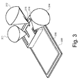
- FIG. 3 be different radiation properties of in FIG. 2 shown antennas shown. These are, in particular, main emission directions or main lobes of these antennas.
- the lobes 311 and 312 are associated with the antenna 215 and the lobe 314 is associated with the antenna 218.
- the emission characteristic is exaggerated in the figures for illustration and is not normally so strongly directed but rather is potato or egg-shaped. It should be understood, however, that at some positions radiation is not necessary or not desired, and therefore the antistatic material may also be provided there, such as on the speaker part / receiver part of a mobile phone.
- FIG. 4 For example, a complete housing 420 receiving the antennas and transmitter module is shown and how the radiation would be through such a housing. Assuming that the housing 420 is made entirely of an antistatic material, significant attenuation of the radiated electromagnetic waves would result, which may lead to the above-described loss of function. For example, the range of the radio signal would be drastically shortened and the attenuation would degrade the signal-to-noise ratio, which would result in erroneous transmission of data.
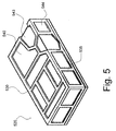
- FIG. 5 shows a frame structure of a housing of a portable electronic device according to an embodiment of the invention.
- Various frame members 530 are shown on the back, bottom and side surfaces.
- the frame structure of the frame members 530 and 535 forms a coherent net, that is, the frame members are all interconnected.
- continuous conductivity is effected between the frame members so that charges can be dissipated, and charges can not accumulate on individual elements, which could cause potential differences between the elements.
- the areas are dimensioned such that they are each no larger than 20 cm 2 , whereby the possible surface charge is limited to the areas.
- plastic for the housing
- simple injection molding techniques can be used to create any frame structures that are thus arbitrarily adaptable to the radiation characteristics of the antennas used in the device.
- the part of the overall housing 520 made of the other material can be made and then coated with the part in FIG FIG. 5 shown frame structure, which can dissipate on the areas accumulating charge due to their lower resistance.
- FIG. 6 For example, the radiation lobes 311, 312 and 314 of FIG Figures 3 and 4 the housing 520 of FIG. 5 superimposed.
- the frame structure with frame elements 530 and 535 off FIG. 5 has been chosen so that the emission lobes pass mainly through the non-antistatic regions, and are thus not adversely affected by the frame elements.
- the radiations of the antenna or antennas and the frame structure are matched to one another such that one main radiation direction, eg the main lobe, passes through an area with the other material.
- the developer of the device must consider the requirements of the radio technology (positioning of the antenna and its radiation characteristics) and the antistatic requirements.
- a retrofit process can be used to fabricate a portable electronic device with static charge protection.
- a conventional portable electronic device with transmitter module, antenna and housing is provided, as well as a frame structure meshed with frame elements made of antistatic material and areas therebetween without material or with material of lower conductivity, i. greater resistance, is formed.
- the frame structure is applied to at least a portion of the housing, e.g. by gluing or screwing or by simply spanning over the housing.
- the frame structure of frame elements made of antistatic material with areas located therebetween without material or other material is arranged on the housing such that the radiation of the antenna passes substantially through the areas and not by the frame elements of antistatic material. For example, fewer and narrower frame elements are used in the area of the antenna than at other positions.
- Various materials, such as certain films or appropriately plasticized plastics, can be used to make the frame structure.
- Portable electronic devices which should usefully have a housing as described above or can be retrofitted accordingly, include portable computers or laptops, personal digital assistants, cell phones, measurement and / or calibration devices, bar code scanners, digital cameras and tablet computers.
- bar code scanners are also desired in factories with explosive environments, where the bar code scanner can detect a bar code in production, and can immediately send the corresponding read information wirelessly by an electromagnetic wave to a computer system in real time, e.g. via Wi-Fi, Bluetooth or other communication technology.
- Wi-Fi Wireless Fidelity
- Bluetooth Wireless Fidelity
- measurement data collected by measurement and / or calibration devices that must be transmitted to a computer system for real-time or near real-time processing.
Landscapes
- Engineering & Computer Science (AREA)
- Microelectronics & Electronic Packaging (AREA)
- Computer Networks & Wireless Communication (AREA)
- Elimination Of Static Electricity (AREA)
- Telephone Set Structure (AREA)
Abstract
Description
- Die vorliegende Erfindung betrifft ein tragbares elektronisches Gerät mit einem Schutz vor statischer Aufladung, das insbesondere zur Verwendung in explosionsgefährdeten Bereichen geeignet ist, sowie ein Verfahren zur Herstellung desselben.
- Elektrostatische Entladungen können bekanntermaßen beispielsweise durch eine Person hervorgerufen werden, die beim Laufen über einen Teppichboden aufgrund von Reibungselektrizität statisch aufgeladen wurde. Dabei können Spannungen von mehreren tausend Volt erreicht werden. Diese elektrostatische Aufladung führt beispielsweise dann zu Problemen, wenn diese Person mit empfindlicher Elektronik arbeitet, wie zum Beispiel bei der Wartung und Handhabung von Computertechnik.
- Genauso wie Personen elektrostatisch aufgeladen werden können, können elektronische Geräte aufgeladen werden, beispielsweise indem eine aufgeladene Person solch ein Gerät anfasst oder das Gerät einfach mit einem Lappen abgewischt wird. Eine elektrostatische Aufladung eines Gehäuses eines elektronischen Geräts kann schon dadurch erfolgen, dass es aus einer Tasche gezogen wird, wodurch Elektronen, negative Ladungen, abgestreift werden können, so dass sich das Gerät auflädt.
- Während sich Personen im Alltag lediglich kurz erschrecken, wenn die auf ihnen befindliche Ladung bei Berührung eines geerdeten Objekts, z.B. Heizkörper, abgeleitet wird, kann dies bei der Handhabung von Schaltkreisen der Computertechnik zur Zerstörung von integrierten Schaltungen, insbesondere von MOSFETs, führen.
- Weitaus schlimmere Folgen können elektrische Entladungen in explosionsgefährdeten Umgebungen, wie z.B. in Kohlebergwerken, Chemiefabriken, Tankstellen, etc. haben. Dort kann ein durch eine Potenzialdifferenz entstehender Funke oder Durchschlag, d.h. eine elektrostatische Entladung, zu einer Entzündung bzw. Explosion von Gas, wie z.B. Grubengas, führen. Grubengas besteht größtenteils aus Methan und kann leicht entzündet werden. Deshalb ist das Unterdrücken eines durch elektrische Entladung erzeugten Funkens in explosionsgefährdeten Bereichen, wie im Ex-Bereich (Zone 1), von äußerster Wichtigkeit.
- Eine Möglichkeit einen gewissen Schutz vor elektrischer Entladung bereitzustellen, besteht darin, elektronische Geräte mit einem antistatischen Gehäuse auszustatten. Jedoch können solche Gehäuse zu einer Beeinträchtigung der Funktion des elektronischen Geräts führen. Diese Gehäuse müssen zuverlässig vor Staub und Nässe schützen sowie auch stabil sein und den verschiedenen Belastungen und Anforderungen im Arbeitsumfeld genügen. Bei elektronischen Geräten, die auf eine Datenübertragung per Funk unter Verwendung einer elektromagnetischen Welle angewiesen sind, führen solche Gehäuse jedoch dazu, dass ausgesandte oder zu empfangende elektromagnetische Wellen stark abgeschwächt werden, was zu Fehlfunktionen oder fehlerhaft empfangenen/gesendeten Daten führen kann.
- Der Erfindung liegt die Aufgabe zugrunde, ein tragbares elektronisches Gerät mit einem Schutz vor statischer Aufladung bereitzustellen, das jedoch in seinen Funktionen nicht eingeschränkt wird.
- Diese Aufgabe wird durch ein elektronisches Gerät mit Schutz vor statischer Aufladung mit den Merkmalen des Anspruchs 1 gelöst. Vorteilhafte Ausführungsformen sind in den Unteransprüchen beschrieben.
- Gemäß einer Ausführungsform umfasst das tragbare elektronische Gerät mit Schutz vor statischer Aufladung ein Sendemodul mit einer Antenne und ein Gehäuse, das unter anderem das Sendemodul und die Antenne aufnimmt. Das tragbare elektronische Gerät ist dabei derart ausgebildet, dass mindestens ein Teil des Gehäuses eine derartige Rahmenstruktur von Rahmenelementen aus antistatischem Material mit dazwischen befindlichen Bereichen eines anderen Materials aufweist, so dass die Abstrahlung der Antenne im Wesentlichen durch die Bereiche geht und nicht durch die Rahmenelemente aus antistatischem Material. Dadurch kann ein stabiles vor statischen Entladungen geschütztes Gehäuse für ein tragbares elektronisches Gerät bereitgestellt werden, das die Funktionen des Geräts nicht beeinträchtigt, und insbesondere abzustrahlende bzw. zu empfangende elektromagnetische Wellen nicht wesentlich beeinflusst, indem die Gehäusestruktur auf die Abstrahlung von einer oder mehreren Antennen im Gerät ausgerichtet ist.
- Gemäß einer vorteilhaften Ausführungsform umfasst das Gehäuse des tragbaren elektronischen Geräts Bereiche aus dem anderen Material, die maximal 20 cm2 groß sind. Bevorzugt sind diese zwischen den Rahmenelementen liegende Bereiche maximal 4 cm2 groß. Dadurch können bestimmte Bereiche des Gehäuses des Geräts auf eine Flächengröße reduziert werden, auf der sich nicht genügend Ladungen sammeln können, um eine derartige Entladung zu bewirken, die in einer explosionsgefährdeten Umgebung eine Explosion durch einen Funken hervorrufen könnte.
- Gemäß einer weiteren vorteilhaften Ausführungsform umfasst das Gehäuse mindestens zwei und bevorzugt mindestens drei Bereiche des anderen, d.h. nicht-antistatischen oder weniger antistatischen Materials. Dadurch können Abstrahlungs- bzw. Empfangsfenster im Gehäuse bereitgestellt werden, die eine Abstrahlungscharakteristik der Antenne oder Antennen nicht merklich negativ beeinflusst und die Funktionen des Geräts nicht beeinträchtigt.
- Gemäß einer weiteren vorteilhaften Ausführungsform sind mindestens zwei Bereiche an der Rückseite des Geräts und/oder zwei Bereiche an den Seitenflächen des Geräts angeordnet. Alternativ kann auch jeweils ein Bereich auf der Rückseite und den beiden Seitenflächen bereitgestellt werden. Somit kann eine effiziente Abstrahlung in verschiedene Raumrichtungen gewährleistet werden.
- Gemäß einer weiteren vorteilhaften Ausführungsform umfasst das antistatische Material einen Kunststoff mit Füllstoffen zum Hervorrufen der antistatischen Eigenschaft. Somit wird ein leichtes Verarbeiten ermöglicht und ein günstiges Material für ein tragbares elektronisches Gerät kann verwendet werden, das weiterhin unempfindlich gegen Nässe, Staub und Stößen ist.
- Gemäß einer weiteren vorteilhaften Ausführungsform ist der Widerstand des antistatischen Materials kleiner als 1011 Ohm und bevorzug kleiner als 109 Ohm. Somit wird ein antistatisches Material gewählt, das einen Widerstand besitzt, der kleiner ist als der des anderen Materials der zwischen den Rahmenelementen befindlichen Bereiche, und ein Aufladen des Gehäuses wird derart unterdrückt, dass einzelnen Ladungen keine Gefährdung in beispielsweise einer explosionsgefährdeten Umgebung darstellen.
- Gemäß einer anderen Ausführungsform bilden die Rahmenelemente, d.h. alle Rahmenelemente der Rahmenstruktur des Geräts ein zusammenhängendes Netz, das eine durchgängige Leitfähigkeit zwischen den Rahmenelementen bewirkt. Somit kann sich keine Ladung auf einzelnen Elementen ansammeln und insbesondere keine Potenzialunterschiede bewirken.
- Gemäß einer anderen Ausführungsform ist die Rahmenstruktur derart ausgebildet, dass ein Benutzer bei normaler Benutzung des tragbaren elektronischen Geräts in Kontakt mit mindestens einem Rahmenelement kommt. Beispielsweise werden Rahmenelemente auf der Rückseite, eines Geräts, die in der Hand eines Benutzers liegt oder Rahmenelemente an einem Handgriff des Geräts vorgesehen. Somit kann ein geerdeter Benutzer gleichzeitig auch das Gehäuse des Geräts erden, indem Ladungen von diesem abgeführt werden können.
- Gemäß einer anderen Ausführungsform sind die Abstrahlungen der Antenne und die Rahmenstruktur derart aufeinander abgestimmt, dass die Hauptstrahlungsrichtung der Antenne durch einen Bereich mit dem anderen Material geht. Dadurch kann eine Abschwächung einer ausgesandten elektromagnetischen Welle größtenteils vermieden werden.
- Gemäß einer anderen vorteilhaften Ausführungsform stellt das Gerät mindestens eines dar von einem tragbaren Computer oder Laptop, einem persönlichen digitalen Assistenten (PDA), einem Mobiltelefon, einem Mess- und/oder Kalibrierungsgerät, einem Barcode-Scanner, einer Digitalkamera und einem Tablet-Computer. Demgemäß können verschiedene tragbare elektronische Geräte gemäß der erfinderischen Lehre angepasst werden und in explosionsgefährdeten Umgebungen sicher verwendet werden.
- Eine weitere Ausführungsform betrifft ein Verfahren zur Herstellung eines tragbaren elektronischen Geräts mit Schutz vor statischer Aufladung, umfassend die Schritte Bereitstellen eines tragbaren elektronischen Geräts mit Sendemodul, Antenne und Gehäuse, und Aufbringen auf mindestens einem Teil des Gehäuses einer Rahmenstruktur von Rahmenelementen (130, 135) aus antistatischem Material mit dazwischen befindlichen Bereichen (140, 141, 142) ohne Material oder eines anderen Materials, so dass die Abstrahlung der Antenne im Wesentlichen durch die Bereiche geht und nicht durch die Rahmenelemente aus antistatischem Material.
- Weitere vorteilhafte Merkmale der Erfindung werden in der detaillierten Beschreibung der Ausführungsformen und in den Ansprüchen offenbart.
- Im Folgenden wird die Erfindung ausführlich anhand der beigefügten Zeichnungen beschrieben.
-
Figuren 1a und 1b zeigen eine Seiten- bzw. Rückansicht eines tragbaren elektrostatischen Geräts gemäß einer Ausführungsform. -
Figur 2 zeigt ein Sendemodul mit Antenne eines tragbaren elektronischen Geräts. -
Figur 3 zeigt die Abstrahlungscharakteristik der Antenne bzw. Antennen derFigur 2 . -
Figur 4 zeigt die Abstrahlungscharakteristik von Antennen eines Sendemoduls in einem Gehäuse. -
Figur 5 zeigt ein Gehäuse mit einer Rahmenstruktur von Rahmenelementen aus antistatischem Material gemäß einer Ausführungsform. -
Figur 6 zeigt wie die Rahmenstruktur des Gehäuses vonFigur 5 passend zur Abstrahlungscharakteristik der Antennenabstrahlungen vonFiguren 3 und4 gewählt wird. - Bevorzugte Ausführungsformen der vorliegenden Erfindung werden nachfolgend ausführlich unter Bezugnahme auf die begleitenden Zeichnungen beschrieben. Dabei sind in den verschiedenen Zeichnungen gleiche oder entsprechende Elemente jeweils mit den gleichen oder ähnlichen Bezugszeichen bezeichnet.
- Die bevorzugten Ausführungsformen der Erfindung, die im Folgenden detailliert beschrieben werden, werden ausführlich mit Bezug auf ein tragbares elektronisches Gerät mit sechs Seitenflächen und einem Sendemodul beschrieben. Jedoch wird bemerkt, dass die vorliegende Beschreibung nur Beispiele enthält und nicht als die Erfindung einschränkend angesehen werden sollte. Beispielsweise kann das tragbare elektronische Gerät auch andere Gehäuseformen mit einer anderen Anzahl von Seitenflächen aufweisen und mehrere Sendemodule oder ein Sende-und Empfangsmodul sowie eine beliebige Anzahl von Antennen enthalten.
-
Figuren 1a und 1b zeigen eine Seitenansicht bzw. Rückseitenansicht eines elektronischen Geräts 100. Durch die schraffierten und nicht-schraffierten Flächen werden unterschiedliche Materialien im Aufbau des Gehäuses 120 des elektronischen Geräts 100 dargestellt, was im Folgenden näher erläutert wird. - Im Einzelnen zeigt
Figur 1a Elemente eines tragbaren elektronischen Geräts zur Verwendung in explosionsgefährdeten Umgebungen. Der Aufbau des Geräts bietet einen Schutz vor statischer Aufladung. Dafür wird ein Gehäuse verwendet, das Rahmenelemente aus antistatischem Material aufweist. Wie gezeigt, umfasst das Gerät 100 ein Sendemodul 110, das auch als Sende- und Empfangsmodul (Transceiver-Modul) ausgebildet sein kann. Dieses Modul 110 weist eine Antenne auf zum Kommunizieren mit anderen Geräten, wie beispielsweise zum Übertragen von Daten an einen Computer oder Empfangen von Anweisungen von einem Computer. - In
Figur 1a ist das Gehäuse 120 von einer Seitenansicht gezeigt. Auf dieser gezeigten Seite weist das Gehäuse eine Rahmenstruktur mit einem Rahmenelement 130 (inFigur 1a schraffiert), das aus antistatischem Material besteht, und einem Bereich 140 (der transparent gezeichnet ist), der aus einem anderen Material besteht, auf. Wie gezeigt, ist der andere Bereich derart angeordnet, dass eine mögliche Abstrahlung einer mit dem Sendemodul verbundenen Antenne durch diesen Bereich gehen kann. - Ähnlich dazu zeigt die in
Figur 1b gezeigte Rückansicht des Geräts 100, dass das Gehäuse 120 auch ein Rahmenelement 135 als Teil der Rahmenstruktur aufweist, das aus antistatischem Material besteht sowie zwischen dem Rahmenelement befindliche Bereiche 141, 142. Da die Bereiche 141, 142 transparent gezeichnet sind, wie inFigur 1a , ist auch ersichtlich, dass ein Sendemodul 110 mit einer Antenne derart im Gehäuse angeordnet ist, dass eine Abstrahlung der Antenne durch insbesondere den linken Bereich 141 gehen kann. - Aus
Figuren 1a und 1b wird ersichtlich, dass mindestens ein Teil des Gehäuses 120 eine derartige Rahmenstruktur von Rahmenelementen 130, 135 aus antistatischem Material mit dazwischen befindlichen Bereichen 140, 141, 142 eines anderen Materials aufweist, dass die Abstrahlung der Antenne des Sendemoduls 110 im Wesentlichen durch die Bereiche 140, 141 geht und nicht durch die Rahmenelemente aus antistatischem Material. Aufgrund der Positionierung der Antenne in diesem Beispiel, wird auch ersichtlich, dass der Bereich 142 weggelassen werden kann, d.h. der Bereich könnte auch durch antistatisches Material ersetzt werden. - Insbesondere kann sich die Rahmenstruktur über alle Seiten des tragbaren elektronischen Geräts 100 erstrecken und aus mehreren Rahmenelementen, z.B. Seitenelementen, aus antistatischem Material bestehen. Dadurch wird eine netzartige Struktur um das Gerät gebildet. Die Bereiche, die zwischen den Rahmenelementen liegen, d.h. von antistatischem Material freigelassene Bereiche, bestehen aus einem anderen Material, das keine oder nur viel geringere antistatische Eigenschaften im Vergleich zu den Rahmenelementen aufweist und dadurch Fenster zur Abstrahlung von elektromagnetischen Wellen bildet.
- Dieses andere Material ist beispielsweise ein normaler für Gehäuse von elektronischen Geräten verwendeter Kunststoff, der im Wesentlichen für elektromagnetische Strahlung mit Frequenzen, die in der Kommunikationstechnik verwendet werden, durchlässig ist. Wie gezeigt, sind die Rahmenelemente derart angeordnet, dass sie die Abstrahlung nur unwesentlich beeinflussen, was im Folgenden noch genauer mit Bezug auf
Figur 6 gezeigt wird. - Im Gegensatz dazu handelt es sich bei dem antistatischen Material um ein Material, das einen geringeren Widerstand aufweist als das andere Material und somit für Ladungen weitgehend leitend ist, so dass diese abgeführt werden können, wodurch sich keine oder nur eine minimale Oberflächenladung bilden kann. Diese antistatische Eigenschaft, d.h. eine Vermeidung der statischen Aufladung, kann beispielsweise durch einen Füllstoff in einem Kunststoff erreicht werden.
- In einer Ausführungsform wird ein antistatisches Material aus einem Kunststoff mit Füllstoffen zum Hervorrufen der antistatischen Eigenschaft erhalten. Als Füllstoffe können beispielsweise Ruß oder verschiedene Salze verwendet werden, wodurch sich auch leicht der Widerstand des antistatischen Materials je nach Dosierung des Füllstoffs einstellen lässt.
- Der Widerstand des antistatischen Materials sollte kleiner als 1011 Ohm gewählt werden und bevorzugt kleiner als 109 Ohm. Die zu wählenden Widerstandswerte sind dabei abhängig von der Anwendungsumgebung. So hat sich gezeigt, dass bei hoher Luftfeuchtigkeit ein Widerstand mit 1011 Ohm ausreichend ist, die oben beschriebene Schutzfunktion zu erfüllen. Anderseits sollte bei niedrigeren Luftfeuchtigkeiten, oder falls diese stark schwankt, höchstens ein Widerstand von ungefähr 109 Ohm gewählt werden. Natürlich kann bei Wahl eines geringen oder geringeren Widerstands als 109 Ohm auch ein grobmaschigeres Netz, d.h. Rahmenstruktur, verwendet werden. In anderen Worten wählt der Entwickler einen guten Kompromiss zwischen Widerstand des antistatischen Materials und Größe der dazwischen befindlichen Bereiche, auf die im Folgenden noch näher eingegangen wird.
- Im Gegensatz zum Widerstand des antistatischen Materials kann der Widerstand des anderen Materials, das bevorzugt auch ein Kunststoff ist, aufgrund der Rahmenstruktur größer sein als 1012 Ohm und liegt normalerweise im Bereich von 1012 bis 1015 Ohm.
- Um eine sich auf den anderen Bereichen ansammelnde Flächenladung wirksam zu begrenzen, wird die Größe jedes zwischen Rahmenelementen liegenden Bereichs nicht größer als, d.h. maximal, 20 cm2 gewählt. Es hat sich gezeigt, dass diese Bereichsgröße einen wirksamen Schutz vor Entladungen insbesondere im Ex-Bereich der Zone 1 bietet. Dies bedeutet, dass beispielsweise bei tragbaren Computern (Laptops) mehrere Bereiche mit einer Größe von bis zu 20 cm2 vorkommen können, um einen wirksamen Schutz vor statischer Aufladung bereitzustellen. Diese Bereiche dürfen jedoch nicht miteinander verbunden sein, so dass durch deren Trennung sichergestellt wird, dass sich Flächenladungen einzelner Bereiche nicht addieren. Durch die Notwendigkeit des Auseinanderhaltens bzw. Isolierens von einzelnen Bereichen werden Rahmenelemente bereitgestellt, die netzartig das Gehäuse bedecken und einzelne Fenster aus dem anderen Material Bereiche von begrenzter Größe erlauben.
- Falls sehr hohe Ansprüche an die Vermeidung der Aufladung eines Bereiches gestellt werden, wie in hochexplosiven Umgebungen oder/und der Widerstand des antistatischen Materials im oben beschriebenen höheren Bereich ist, können die Bereiche auch bevorzugt maximal 4 cm2 gewählt werden. Der Vorteil bei der netzartigen Ausbildung der Rahmenstruktur des Gehäuses ist dabei, dass beliebige Bereichsgrößen leicht hergestellt werden können.
- Wie mit Bezug auf
Figuren 1a und 1b beschrieben, umfasst das Gehäuse mindestens zwei und bevorzugt mindestens drei Bereiche des anderen Materials. Beispielsweise können zwei Bereiche auf der Rückseite des Gehäuses vorgesehen werden, wie inFigur 1b gezeigt. Des Weiteren kann auch jeweils ein Bereich auf jeweils einer der zwei Seitenflächen bereitgestellt werden, wie inFigur 1a gezeigt. Um mehrere Raumrichtungen abzudecken, ist es gemäßFiguren 1a und 1b auch möglich, jeweils auf beiden Seitenflächen einen Bereich 140 vorzusehen und auf der Rückseite des Gehäuses einen Bereich 141, so dass drei Bereiche des anderen Materials eine nahezu unbeschränkte Abstrahlung in mindestens einem 180° Bereich ermöglichen. Der Einfluss auf die Abstrahlung der zwei Rahmenelemente, die den 180° Bereich in drei Bereiche aufteilen, ist vernachlässigbar. - Je nachdem wie viele Empfangs- bzw. Sendemodule und Antennen verwendet werden oder bei komplizierten Abstrahleigenschaften ist es vorteilhaft, mehrere Bereiche auf der Rückseite des Geräts, z.B. zwei, und/oder mehrere Bereiche an den Seitenflächen des Geräts anzuordnen. Natürlich können solche Bereiche auch an der Oberseite und Unterseite oder auch an der Vorderseite des Geräts angeordnet werden.
-
Figur 2 zeigt ein konkretes Beispiel eines Sendemoduls 210 mit zwei Antennen 215 und 218, das von dem Gehäuse des oben beschriebenen tragbaren elektronischen Geräts aufgenommen werden kann. In diesem Beispiel ist das Sendmodul 210 auf einem Träger 250, z.B. einer Platine, angebracht. Dieser Träger 250 liegt wiederum auf einer Platte 230, die beispielsweise einen Teil des Gehäuses, z.B. die Vorderseite des Gehäuses, bildet. In diesem Beispiel wird eine PIF-Antenne (Planar Inverted F-Shaped Antenna) verwendet, welches eine kompakte Antenne ist, die unter anderem in Mobilfunktelefonen eingesetzt wird, und klein, flach, effektiv und günstig herzustellen ist. Diese Antennenart eignet sich somit zur Verwendung in tragbaren elektronischen Geräten. - In
Figur 3 werden verschiedene Abstrahlungseigenschaften der inFigur 2 gezeigten Antennen dargestellt. Hierbei handelt es sich insbesondere um Hauptabstrahlrichtungen bzw. Hauptkeulen dieser Antennen. Die Keulen 311 und 312 sind der Antenne 215 zugeordnet und die Keule 314 ist der Antenne 218 zugeordnet. - Der Fachmann erkennt, dass die Abstrahlcharakteristik in den Figuren zur Illustration übertrieben dargestellt ist und normalerweise nicht derart stark gerichtet ist sondern eher Kartoffel- bzw. Ei-förmig ist. Es soll jedoch verstanden werden, dass an einigen Positionen eine Abstrahlung auch nicht notwendig bzw. nicht erwünscht ist, und daher auch dort das antistatische Material vorgesehen werden kann, wie beispielsweise an dem Lautsprecherteil/Hörerteil eines Mobiltelefons.
- In
Figur 4 wird ein vollständiges die Antennen und Sendemodul aufnehmendes Gehäuse 420 gezeigt, und es wird gezeigt, wie die Abstrahlung durch ein solches Gehäuse erfolgen würde. Unter der Annahme, dass das Gehäuse 420 vollständig aus einem antistatischen Material gefertigt ist, würde es zu signifikanten Abschwächungen bzw. Dämpfungen der abgestrahlten elektromagnetischen Wellen kommen, was zu den oben beschriebenen Funktionseinbußen führen kann. Beispielsweise würde die Reichweite des Funksignals drastisch verkürzt und durch die Abschwächung das Signal-zu-RauschVerhältnis verschlechtert, was zu fehlerhafter Übertragung von Daten führen würde. -
Figur 5 zeigt eine Rahmenstruktur eines Gehäuses eines tragbaren elektronischen Geräts gemäß einer Ausführungsform der Erfindung. Verschiedene Rahmenelemente 530 sind auf der Rückseite, Unterseite und Seitenfläche gezeigt. Insbesondere sind inFigur 5 mehrere zwischen den Rahmenelementen befindliche Bereiche, z.B. die Bereiche 540, 543, 544, vorgesehen, die aus einem Material bestehen, das elektromagnetische Wellen ohne merkliche Abschwächungen durchlässt. - Die Rahmenstruktur aus den Rahmenelementen 530 und 535 bildet ein zusammenhängendes Netz, d.h. die Rahmenelemente sind alle miteinander verbunden. Somit wird eine durchgängige Leitfähigkeit zwischen den Rahmenelementen bewirkt, so dass Ladungen abgeleitet werden können, und Ladungen können sich nicht auf einzelnen Elementen ansammeln, wodurch Potenzialunterschiede zwischen den Elementen entstehen könnten. Zudem sind die Bereiche derartig dimensioniert, dass sie jeweils nicht größer als 20 cm2 sind, wodurch die mögliche Oberflächenladung auf den Bereichen begrenzt wird.
- Aus der gezeigten Art der Rahmenstruktur ist sofort ersichtlich, dass ein Benutzer bei normaler Benutzung des tragbaren elektronischen Geräts, d.h. beim In-die-Hand-nehmen des Gehäuses 520, der Benutzer in Kontakt mit mindestens einem Rahmenelement kommt. Da diese Rahmenelemente jedoch alle miteinander verbunden sind, kann der Benutzer als Erdung des Gehäuses fungieren, was insbesondere vorteilhaft ist, wenn der Benutzer selbst geerdet ist.
- Durch die Verwendung von Kunststoff für das Gehäuse können einfache Spritzgussverfahren verwendet werden, um beliebige Rahmenstrukturen zu erzeugen, die somit beliebig anpassbar sind auf Abstrahlungseigenschaften der verwendeten Antennen im Gerät. Beispielsweise kann zuerst der Teil des Gesamtgehäuses 520, der aus dem anderen Material besteht, hergestellt werden und danach dieser überzogen werden mit der in
Figur 5 gezeigten Rahmenstruktur, die auf den Bereichen sich ansammelnde Ladung aufgrund ihres niedrigeren Widerstands abführen kann. - In
Figur 6 werden die Abstrahlungskeulen 311, 312 und 314 derFiguren 3 und4 dem Gehäuse 520 derFigur 5 überlagert. Dabei zeigt sich, dass die Rahmenstruktur mit Rahmenelementen 530 und 535 ausFigur 5 derart passend gewählt wurde, dass die Abstrahlungskeulen hauptsächlich durch die nicht-antistatischen Bereiche gehen, und dadurch nicht durch die Rahmenelemente negativ beeinflusst werden. Mit anderen Worten ausgedrückt, sind die Abstrahlungen der Antenne oder Antennen und die Rahmenstruktur derart aufeinander abgestimmt, dass eine Hauptstrahlungsrichtung, z.B. die Hauptkeule, durch einen Bereich mit dem anderen Material geht. - Somit besteht eine Abhängigkeit zwischen der Antennenform und den daraus resultierenden Abstrahlungseigenschaften der Antenne und der Art der zu verwendeten Rahmenstruktur für das Gehäuse. Daher muss der Entwickler des Geräts die Anforderungen der Funktechnik (Positionierung der Antenne und deren Abstrahlungseigenschaften) und die der Antistatik in Betracht ziehen.
- Aus der vorangegangenen Diskussion wird deutlich, dass es auch möglich ist, insbesondere durch Kenntnis der Abstrahlungseigenschaften der Antenne und der Möglichkeit der einfachen Herstellung einer Rahmenstruktur aus antistatischem Material, eine für existierende Geräte, die nicht mit einem Schutz vor statischer Aufladung versehen sind, entsprechende Rahmenstruktur zu fertigen, die dann auf einem existierenden Gehäuse des Geräts aufgebracht werden kann.
- Demgemäß kann ein Nachrüstungsprozess verwendet werden zur Herstellung eines tragbaren elektronischen Geräts mit Schutz vor statischer Aufladung. Dabei wird in einem ersten Schritt ein herkömmliches tragbares elektronisches Gerät mit Sendemodul, Antenne und Gehäuse bereitgestellt sowie eine Rahmenstruktur, die netzartig mit Rahmenelementen aus antistatischem Material und dazwischen befindlichen Bereichen ohne Material oder mit Material einer geringeren Leitfähigkeit, d.h. größerem Widerstand, ausgebildet ist.
- Danach wird die Rahmenstruktur auf mindestens einem Teil des Gehäuses aufgebracht, z.B. durch Kleben oder Schrauben oder durch einfaches Überspannen über das Gehäuse. Dabei wird die Rahmenstruktur aus Rahmenelementen aus antistatischem Material mit dazwischen befindlichen Bereichen ohne Material oder eines anderen Materials derart auf dem Gehäuse angeordnet, dass die Abstrahlung der Antenne im Wesentlichen durch die Bereiche geht und nicht durch die Rahmenelemente aus antistatischem Material. Beispielsweise werden im Bereich der Antenne weniger und schmalere Rahmenelemente verwendet als an anderen Positionen. Verschiedene Materialien wie bestimmte Folien oder entsprechend auf den Widerstand angepasste Kunststoffe können zur Herstellung der Rahmenstruktur verwendet werden.
- Tragbare elektronische Geräte, die sinnvollerweise ein Gehäuse gemäß den obigen Ausführungen aufweisen sollten oder dementsprechend nachgerüstet werden können, umfassen tragbare Computer oder Laptops, persönliche digitale Assistenten, Mobiltelefone, Mess- und/oder Kalibrierungsgeräte, Barcode-Scanner, Digitalkameras und Tablet-Computer.
- Beispielsweise ist die Verwendung von Barcode-Scannern auch in Fabriken mit explosionsgefährdeten Umgebungen gewünscht, wobei der Barcode-Scanner einen Barcode in der Produktion erfassen kann, und die entsprechenden ausgelesenen Informationen sofort drahtlos durch eine elektromagnetische Welle an ein Computersystem in Echtzeit senden kann, z.B. über WLAN, Bluetooth oder eine andere Kommunikationstechnologie. Das gleiche gilt für Messdaten, die von Mess- und/oder Kalibrierungsgeräten erfasst werden und zur Echtzeit- oder Nahe-Echtzeitverarbeitung an ein Computersystem übertragen werden müssen.
- Aus der vorangehenden Beschreibung erkennt der Fachmann, dass verschiedene Modifikationen und Varianten des Geräts möglich sind, ohne den Umfang der durch die Ansprüche definierten Erfindung zu verlassen. Ferner wurde die Erfindung mit Bezug auf bestimmte Beispiele beschrieben, die jedoch nur zum besseren Verständnis der Erfindung dienen sollen, und diese nicht einschränken sollen. Der Fachmann erkennt auch sofort, dass viele verschiedene Kombinationen der beschriebenen Elemente zur Ausführung der vorliegenden Erfindung verwendet werden können. Deshalb wird der wahre Umfang der Erfindung durch die folgenden Ansprüche gekennzeichnet.
Claims (11)
- Tragbares elektronisches Gerät mit Schutz vor statischer Aufladung, umfassend
ein Sendemodul (110) mit einer Antenne, und
ein Gehäuse (120), das das Sendemodul und die Antenne aufnimmt, wobei
mindestens ein Teil des Gehäuses eine derartige Rahmenstruktur von Rahmenelementen (130, 135) aus antistatischem Material mit dazwischen befindlichen Bereichen (140, 141, 142) eines anderen Materials aufweist, dass die Abstrahlung der Antenne im Wesentlichen durch die Bereiche geht und nicht durch die Rahmenelemente aus antistatischem Material. - Tragbares elektronisches Gerät nach Anspruch 1, wobei die Größe jedes Bereichs maximal 20 cm2 oder bevorzugt maximal 4 cm2 ist.
- Tragbares elektronisches Gerät nach Anspruch 1 oder 2, wobei das Gehäuse mindestens zwei und bevorzugt mindestens drei Bereiche des anderen Materials umfasst.
- Tragbares elektronisches Gerät nach einem der Ansprüche 1 bis 3, wobei mindestens zwei Bereiche an der Rückseite des Geräts und/oder zwei Bereiche an den Seitenflächen des Geräts angeordnet sind.
- Tragbares elektronisches Gerät nach einem der Ansprüche 1 bis 4, wobei das antistatische Material ein Kunststoff mit Füllstoffen zum Hervorrufen der antistatischen Eigenschaft ist.
- Tragbares elektronisches Gerät nach einem der Ansprüche 1 bis 5, wobei der Widerstand des antistatischen Materials kleiner als 1011 Ohm bevorzugt kleiner als 109 Ohm ist.
- Tragbares elektronisches Gerät nach einem der Ansprüche 1 bis 6, wobei die Rahmenelemente der Rahmenstruktur des Geräts ein zusammenhängendes Netz bilden, das eine durchgängige Leitfähigkeit zwischen den Rahmenelementen bewirkt.
- Tragbares elektronisches Gerät nach einem der Ansprüche 1 bis 7, wobei die Rahmenstruktur derart ausgebildet ist, dass ein Benutzer bei normaler Benutzung des tragbaren elektronischen Geräts in Kontakt mit mindestens einem Rahmenelement kommt.
- Tragbares elektronisches Gerät nach einem der Ansprüche 1 bis 8, wobei die Abstrahlung der Antenne und die Rahmenstruktur derart aufeinander abgestimmt sind, dass die Hauptstrahlungsrichtung durch einen Bereich mit dem anderen Material geht.
- Tragbares elektronisches Gerät nach einem der Ansprüche 1 bis 9, wobei das Gerät mindestens eines darstellt von einem tragbaren Computer oder Laptop, einem Persönlichen Digitalen Assistenten, einem Mobiltelefon, einem Mess-und/oder Kalibrierungsgerät, einem Barcode-Scanner, einer Digitalkamera und einem Tablet-Computer.
- Verfahren zur Herstellung eines tragbaren elektronischen Geräts mit Schutz vor statischer Aufladung, umfassend die Schritte:Bereitstellen eines tragbaren elektronischen Geräts mit Sendemodul, Antenne und Gehäuse, undAufbringen auf mindestens einem Teil des Gehäuses einer Rahmenstruktur von Rahmenelementen (130, 135) aus antistatischem Material mit dazwischen befindlichen Bereichen (140, 141, 142) ohne Material oder eines anderen Materials, so dass die Abstrahlung der Antenne im Wesentlichen durch die Bereiche geht und nicht durch die Rahmenelemente aus antistatischem Material.
Applications Claiming Priority (1)
| Application Number | Priority Date | Filing Date | Title |
|---|---|---|---|
| DE102013201372.8A DE102013201372B4 (de) | 2013-01-29 | 2013-01-29 | Tragbares elektronisches Gerät mit Schutz vor statischer Aufladung |
Publications (4)
| Publication Number | Publication Date |
|---|---|
| EP2760263A2 true EP2760263A2 (de) | 2014-07-30 |
| EP2760263A3 EP2760263A3 (de) | 2017-11-08 |
| EP2760263C0 EP2760263C0 (de) | 2024-03-27 |
| EP2760263B1 EP2760263B1 (de) | 2024-03-27 |
Family
ID=50023436
Family Applications (1)
| Application Number | Title | Priority Date | Filing Date |
|---|---|---|---|
| EP14152625.1A Active EP2760263B1 (de) | 2013-01-29 | 2014-01-27 | Tragbares elektronisches Gerät mit Schutz vor statischer Aufladung |
Country Status (3)
| Country | Link |
|---|---|
| US (1) | US9153858B2 (de) |
| EP (1) | EP2760263B1 (de) |
| DE (1) | DE102013201372B4 (de) |
Families Citing this family (3)
| Publication number | Priority date | Publication date | Assignee | Title |
|---|---|---|---|---|
| US20150138020A1 (en) * | 2013-11-15 | 2015-05-21 | Motorola Solutions, Inc | Intrinsically safe housing and antenna design for a radio device and method of forming same |
| US10582630B1 (en) | 2015-12-28 | 2020-03-03 | Roger Graham | Method and apparatus for managing static electricity |
| US10524370B2 (en) | 2017-06-28 | 2019-12-31 | Seagate Technology Llc | Electrostatic charge build-up prevention for data storage devices |
Family Cites Families (17)
| Publication number | Priority date | Publication date | Assignee | Title |
|---|---|---|---|---|
| NL248852A (de) | 1959-02-27 | |||
| DE4407823C2 (de) | 1994-03-09 | 1997-12-11 | Grieshaber Vega Kg | Füllstandmeßgerät |
| DE19614914A1 (de) | 1996-04-16 | 1997-10-23 | Telesensomatic Gmbh | Transponderanordnung und Verfahren zur Herstellung einer solchen Transponderanordnung |
| US6567047B2 (en) * | 2000-05-25 | 2003-05-20 | Tyco Electronics Logistics Ag | Multi-band in-series antenna assembly |
| US6531985B1 (en) | 2000-08-14 | 2003-03-11 | 3Com Corporation | Integrated laptop antenna using two or more antennas |
| JP2003209419A (ja) * | 2002-01-16 | 2003-07-25 | Toshiba Corp | 電子機器及びアンテナ実装方法 |
| DE102005046306B3 (de) * | 2005-09-27 | 2006-10-26 | Munsch Chemie-Pumpen Gmbh | Behältnis aus schweißbarem, nicht leitendem Kunststoff, welches in einer explosionsgefährdeten Umgebung eingesetzt wird |
| EP1841004A1 (de) | 2006-03-29 | 2007-10-03 | Hueck Folien Ges.m.b.H | Transponder-Antenne auf einem Substrat mit Antistatikbeschichtung |
| US7518568B2 (en) * | 2007-04-27 | 2009-04-14 | Hewlett-Packard Development Company, L.P. | Antenna for an electronic device |
| US8138977B2 (en) * | 2007-08-07 | 2012-03-20 | Apple Inc. | Antennas for handheld electronic devices |
| US7804453B2 (en) * | 2008-04-16 | 2010-09-28 | Apple Inc. | Antennas for wireless electronic devices |
| CN101573009A (zh) * | 2008-04-28 | 2009-11-04 | 富准精密工业(深圳)有限公司 | 电子装置壳体及其制造方法 |
| JP5169777B2 (ja) * | 2008-12-03 | 2013-03-27 | ソニー株式会社 | 携帯端末装置 |
| US8325094B2 (en) * | 2009-06-17 | 2012-12-04 | Apple Inc. | Dielectric window antennas for electronic devices |
| US8896487B2 (en) * | 2009-07-09 | 2014-11-25 | Apple Inc. | Cavity antennas for electronic devices |
| US8269677B2 (en) * | 2009-09-03 | 2012-09-18 | Apple Inc. | Dual-band cavity-backed antenna for integrated desktop computer |
| DE102011003978B4 (de) | 2011-02-11 | 2020-06-04 | Ecom Instruments Gmbh | Schaltungsanordnung zur Leitungssicherung und Modul, das dieselbe enthält |
-
2013
- 2013-01-29 DE DE102013201372.8A patent/DE102013201372B4/de active Active
-
2014
- 2014-01-27 EP EP14152625.1A patent/EP2760263B1/de active Active
- 2014-01-27 US US14/165,483 patent/US9153858B2/en active Active
Non-Patent Citations (1)
| Title |
|---|
| None |
Also Published As
| Publication number | Publication date |
|---|---|
| EP2760263C0 (de) | 2024-03-27 |
| US20140210676A1 (en) | 2014-07-31 |
| DE102013201372A1 (de) | 2014-07-31 |
| US9153858B2 (en) | 2015-10-06 |
| EP2760263A3 (de) | 2017-11-08 |
| EP2760263B1 (de) | 2024-03-27 |
| DE102013201372B4 (de) | 2018-06-07 |
Similar Documents
| Publication | Publication Date | Title |
|---|---|---|
| DE60037966T2 (de) | Touchpad mit integrierter antenne für laptop-computer | |
| DE112017008496B4 (de) | Antennenvorrichtung | |
| DE102011056203B4 (de) | Tragbares Gerät | |
| EP0254964A3 (de) | Magnetische oder elektromagnetische Abschirmung und damit ausgerüstetes elektrisches Kabel | |
| DE202010008162U1 (de) | RFID-Lesevorrichtung | |
| DE102014102190A1 (de) | Klemmstruktur und Tastenmodul | |
| DE102013201372B4 (de) | Tragbares elektronisches Gerät mit Schutz vor statischer Aufladung | |
| DE112018001933T5 (de) | Antenne, Gruppenantenne, Radarvorrichtung und fahrzeuginternes System | |
| DE102016117105A1 (de) | Antenneeinrichtung | |
| DE60219274T2 (de) | Elektronische Vorrichtung | |
| US20150222311A1 (en) | Housing for electrostatic discharge protection of a portable communication device | |
| DE202017106580U1 (de) | Zubehörteil für Mobilgerät ausgerüstet für die Kommunikation mit dem Mobilgerät | |
| DE102018103553A1 (de) | Elektronisches gerät | |
| DE102017112155B4 (de) | Desense-Verringerung mittels Pin-Remap in einem modularen Gerät | |
| DE102018103416A1 (de) | Signalverstärker für ein mobilgerät | |
| DE102015121451A1 (de) | Bausatz für ein modulares Radarsystem | |
| DE102021206859A1 (de) | Radarvorrichtung | |
| DE102013105298A1 (de) | Reinigungsroboter und System unter Verwendung desselben | |
| DE102010055850A1 (de) | Absorber für elektromagnetische Wellen | |
| DE102011102568A1 (de) | Vorrichtung zur Lokalisierung von pulsbasierten Hochleistungsmikrowellen-Waffen | |
| DE202016008742U1 (de) | Frequenzselektive Strukturen zur EMI - Abschwächung | |
| CN111726137B (zh) | 天线功率控制方法、装置及电子设备 | |
| DE102012110170B4 (de) | Modulares Bussystem zur Übertragung von Daten und/oder Energie | |
| DE69914799T2 (de) | Elektrische Vorrichtung zur kontaktlosen Übertragung mit wahlweiser Hilfs- energiequelle | |
| DE102016215459A1 (de) | Segmentiertes Blitzableiterelement mit integriertem ESD-Schutz |
Legal Events
| Date | Code | Title | Description |
|---|---|---|---|
| PUAI | Public reference made under article 153(3) epc to a published international application that has entered the european phase |
Free format text: ORIGINAL CODE: 0009012 |
|
| 17P | Request for examination filed |
Effective date: 20140127 |
|
| AK | Designated contracting states |
Kind code of ref document: A2 Designated state(s): AL AT BE BG CH CY CZ DE DK EE ES FI FR GB GR HR HU IE IS IT LI LT LU LV MC MK MT NL NO PL PT RO RS SE SI SK SM TR |
|
| AX | Request for extension of the european patent |
Extension state: BA ME |
|
| PUAL | Search report despatched |
Free format text: ORIGINAL CODE: 0009013 |
|
| AK | Designated contracting states |
Kind code of ref document: A3 Designated state(s): AL AT BE BG CH CY CZ DE DK EE ES FI FR GB GR HR HU IE IS IT LI LT LU LV MC MK MT NL NO PL PT RO RS SE SI SK SM TR |
|
| AX | Request for extension of the european patent |
Extension state: BA ME |
|
| RIC1 | Information provided on ipc code assigned before grant |
Ipc: H05K 9/00 20060101AFI20170929BHEP |
|
| STAA | Information on the status of an ep patent application or granted ep patent |
Free format text: STATUS: REQUEST FOR EXAMINATION WAS MADE |
|
| R17P | Request for examination filed (corrected) |
Effective date: 20180406 |
|
| RBV | Designated contracting states (corrected) |
Designated state(s): AL AT BE BG CH CY CZ DE DK EE ES FI FR GB GR HR HU IE IS IT LI LT LU LV MC MK MT NL NO PL PT RO RS SE SI SK SM TR |
|
| STAA | Information on the status of an ep patent application or granted ep patent |
Free format text: STATUS: EXAMINATION IS IN PROGRESS |
|
| 17Q | First examination report despatched |
Effective date: 20210617 |
|
| GRAP | Despatch of communication of intention to grant a patent |
Free format text: ORIGINAL CODE: EPIDOSNIGR1 |
|
| STAA | Information on the status of an ep patent application or granted ep patent |
Free format text: STATUS: GRANT OF PATENT IS INTENDED |
|
| INTG | Intention to grant announced |
Effective date: 20231006 |
|
| GRAS | Grant fee paid |
Free format text: ORIGINAL CODE: EPIDOSNIGR3 |
|
| GRAA | (expected) grant |
Free format text: ORIGINAL CODE: 0009210 |
|
| STAA | Information on the status of an ep patent application or granted ep patent |
Free format text: STATUS: THE PATENT HAS BEEN GRANTED |
|
| AK | Designated contracting states |
Kind code of ref document: B1 Designated state(s): AL AT BE BG CH CY CZ DE DK EE ES FI FR GB GR HR HU IE IS IT LI LT LU LV MC MK MT NL NO PL PT RO RS SE SI SK SM TR |
|
| REG | Reference to a national code |
Ref country code: GB Ref legal event code: FG4D Free format text: NOT ENGLISH |
|
| REG | Reference to a national code |
Ref country code: CH Ref legal event code: EP |
|
| REG | Reference to a national code |
Ref country code: DE Ref legal event code: R096 Ref document number: 502014016789 Country of ref document: DE |
|
| REG | Reference to a national code |
Ref country code: IE Ref legal event code: FG4D Free format text: LANGUAGE OF EP DOCUMENT: GERMAN |
|
| U01 | Request for unitary effect filed |
Effective date: 20240328 |
|
| U07 | Unitary effect registered |
Designated state(s): AT BE BG DE DK EE FI FR IT LT LU LV MT NL PT SE SI Effective date: 20240410 |
|
| PG25 | Lapsed in a contracting state [announced via postgrant information from national office to epo] |
Ref country code: GR Free format text: LAPSE BECAUSE OF FAILURE TO SUBMIT A TRANSLATION OF THE DESCRIPTION OR TO PAY THE FEE WITHIN THE PRESCRIBED TIME-LIMIT Effective date: 20240628 |
|
| PG25 | Lapsed in a contracting state [announced via postgrant information from national office to epo] |
Ref country code: RS Free format text: LAPSE BECAUSE OF FAILURE TO SUBMIT A TRANSLATION OF THE DESCRIPTION OR TO PAY THE FEE WITHIN THE PRESCRIBED TIME-LIMIT Effective date: 20240627 Ref country code: HR Free format text: LAPSE BECAUSE OF FAILURE TO SUBMIT A TRANSLATION OF THE DESCRIPTION OR TO PAY THE FEE WITHIN THE PRESCRIBED TIME-LIMIT Effective date: 20240327 |
|
| PG25 | Lapsed in a contracting state [announced via postgrant information from national office to epo] |
Ref country code: RS Free format text: LAPSE BECAUSE OF FAILURE TO SUBMIT A TRANSLATION OF THE DESCRIPTION OR TO PAY THE FEE WITHIN THE PRESCRIBED TIME-LIMIT Effective date: 20240627 Ref country code: NO Free format text: LAPSE BECAUSE OF FAILURE TO SUBMIT A TRANSLATION OF THE DESCRIPTION OR TO PAY THE FEE WITHIN THE PRESCRIBED TIME-LIMIT Effective date: 20240627 Ref country code: HR Free format text: LAPSE BECAUSE OF FAILURE TO SUBMIT A TRANSLATION OF THE DESCRIPTION OR TO PAY THE FEE WITHIN THE PRESCRIBED TIME-LIMIT Effective date: 20240327 Ref country code: GR Free format text: LAPSE BECAUSE OF FAILURE TO SUBMIT A TRANSLATION OF THE DESCRIPTION OR TO PAY THE FEE WITHIN THE PRESCRIBED TIME-LIMIT Effective date: 20240628 |
|
| PG25 | Lapsed in a contracting state [announced via postgrant information from national office to epo] |
Ref country code: IS Free format text: LAPSE BECAUSE OF FAILURE TO SUBMIT A TRANSLATION OF THE DESCRIPTION OR TO PAY THE FEE WITHIN THE PRESCRIBED TIME-LIMIT Effective date: 20240727 |
|
| PG25 | Lapsed in a contracting state [announced via postgrant information from national office to epo] |
Ref country code: SM Free format text: LAPSE BECAUSE OF FAILURE TO SUBMIT A TRANSLATION OF THE DESCRIPTION OR TO PAY THE FEE WITHIN THE PRESCRIBED TIME-LIMIT Effective date: 20240327 |
|
| PG25 | Lapsed in a contracting state [announced via postgrant information from national office to epo] |
Ref country code: ES Free format text: LAPSE BECAUSE OF FAILURE TO SUBMIT A TRANSLATION OF THE DESCRIPTION OR TO PAY THE FEE WITHIN THE PRESCRIBED TIME-LIMIT Effective date: 20240327 |
|
| PG25 | Lapsed in a contracting state [announced via postgrant information from national office to epo] |
Ref country code: CZ Free format text: LAPSE BECAUSE OF FAILURE TO SUBMIT A TRANSLATION OF THE DESCRIPTION OR TO PAY THE FEE WITHIN THE PRESCRIBED TIME-LIMIT Effective date: 20240327 |
|
| PG25 | Lapsed in a contracting state [announced via postgrant information from national office to epo] |
Ref country code: PL Free format text: LAPSE BECAUSE OF FAILURE TO SUBMIT A TRANSLATION OF THE DESCRIPTION OR TO PAY THE FEE WITHIN THE PRESCRIBED TIME-LIMIT Effective date: 20240327 |
|
| PG25 | Lapsed in a contracting state [announced via postgrant information from national office to epo] |
Ref country code: SK Free format text: LAPSE BECAUSE OF FAILURE TO SUBMIT A TRANSLATION OF THE DESCRIPTION OR TO PAY THE FEE WITHIN THE PRESCRIBED TIME-LIMIT Effective date: 20240327 |
|
| PG25 | Lapsed in a contracting state [announced via postgrant information from national office to epo] |
Ref country code: SM Free format text: LAPSE BECAUSE OF FAILURE TO SUBMIT A TRANSLATION OF THE DESCRIPTION OR TO PAY THE FEE WITHIN THE PRESCRIBED TIME-LIMIT Effective date: 20240327 Ref country code: SK Free format text: LAPSE BECAUSE OF FAILURE TO SUBMIT A TRANSLATION OF THE DESCRIPTION OR TO PAY THE FEE WITHIN THE PRESCRIBED TIME-LIMIT Effective date: 20240327 Ref country code: RO Free format text: LAPSE BECAUSE OF FAILURE TO SUBMIT A TRANSLATION OF THE DESCRIPTION OR TO PAY THE FEE WITHIN THE PRESCRIBED TIME-LIMIT Effective date: 20240327 Ref country code: PL Free format text: LAPSE BECAUSE OF FAILURE TO SUBMIT A TRANSLATION OF THE DESCRIPTION OR TO PAY THE FEE WITHIN THE PRESCRIBED TIME-LIMIT Effective date: 20240327 Ref country code: IS Free format text: LAPSE BECAUSE OF FAILURE TO SUBMIT A TRANSLATION OF THE DESCRIPTION OR TO PAY THE FEE WITHIN THE PRESCRIBED TIME-LIMIT Effective date: 20240727 Ref country code: ES Free format text: LAPSE BECAUSE OF FAILURE TO SUBMIT A TRANSLATION OF THE DESCRIPTION OR TO PAY THE FEE WITHIN THE PRESCRIBED TIME-LIMIT Effective date: 20240327 Ref country code: CZ Free format text: LAPSE BECAUSE OF FAILURE TO SUBMIT A TRANSLATION OF THE DESCRIPTION OR TO PAY THE FEE WITHIN THE PRESCRIBED TIME-LIMIT Effective date: 20240327 |
|
| REG | Reference to a national code |
Ref country code: DE Ref legal event code: R097 Ref document number: 502014016789 Country of ref document: DE |
|
| PLBE | No opposition filed within time limit |
Free format text: ORIGINAL CODE: 0009261 |
|
| STAA | Information on the status of an ep patent application or granted ep patent |
Free format text: STATUS: NO OPPOSITION FILED WITHIN TIME LIMIT |
|
| U20 | Renewal fee for the european patent with unitary effect paid |
Year of fee payment: 12 Effective date: 20250127 |
|
| 26N | No opposition filed |
Effective date: 20250103 |
|
| REG | Reference to a national code |
Ref country code: CH Ref legal event code: PL |
|
| PG25 | Lapsed in a contracting state [announced via postgrant information from national office to epo] |
Ref country code: MC Free format text: LAPSE BECAUSE OF FAILURE TO SUBMIT A TRANSLATION OF THE DESCRIPTION OR TO PAY THE FEE WITHIN THE PRESCRIBED TIME-LIMIT Effective date: 20240327 |
|
| PG25 | Lapsed in a contracting state [announced via postgrant information from national office to epo] |
Ref country code: CH Free format text: LAPSE BECAUSE OF NON-PAYMENT OF DUE FEES Effective date: 20250131 |
|
| PG25 | Lapsed in a contracting state [announced via postgrant information from national office to epo] |
Ref country code: IE Free format text: LAPSE BECAUSE OF NON-PAYMENT OF DUE FEES Effective date: 20250127 |
|
| U20 | Renewal fee for the european patent with unitary effect paid |
Year of fee payment: 13 Effective date: 20260128 |
|
| PGFP | Annual fee paid to national office [announced via postgrant information from national office to epo] |
Ref country code: GB Payment date: 20260122 Year of fee payment: 13 |