EP2756549B1 - Apparatus and method for use with antenna array - Google Patents
Apparatus and method for use with antenna array Download PDFInfo
- Publication number
- EP2756549B1 EP2756549B1 EP11764793.3A EP11764793A EP2756549B1 EP 2756549 B1 EP2756549 B1 EP 2756549B1 EP 11764793 A EP11764793 A EP 11764793A EP 2756549 B1 EP2756549 B1 EP 2756549B1
- Authority
- EP
- European Patent Office
- Prior art keywords
- signal
- tapering
- power amplifier
- signals
- antenna
- Prior art date
- Legal status (The legal status is an assumption and is not a legal conclusion. Google has not performed a legal analysis and makes no representation as to the accuracy of the status listed.)
- Not-in-force
Links
- 238000000034 method Methods 0.000 title claims description 19
- 230000001276 controlling effect Effects 0.000 claims description 25
- 230000001105 regulatory effect Effects 0.000 claims description 6
- 230000004044 response Effects 0.000 claims description 6
- 238000010295 mobile communication Methods 0.000 claims description 3
- 238000012423 maintenance Methods 0.000 claims description 2
- 230000003321 amplification Effects 0.000 claims 1
- 238000003199 nucleic acid amplification method Methods 0.000 claims 1
- 230000008901 benefit Effects 0.000 description 10
- 230000005540 biological transmission Effects 0.000 description 5
- 239000011159 matrix material Substances 0.000 description 3
- 230000000903 blocking effect Effects 0.000 description 1
- 230000008709 cellular rearrangement Effects 0.000 description 1
- 230000008859 change Effects 0.000 description 1
- 230000003247 decreasing effect Effects 0.000 description 1
- 230000000593 degrading effect Effects 0.000 description 1
- 230000000694 effects Effects 0.000 description 1
- 238000011065 in-situ storage Methods 0.000 description 1
- 238000004519 manufacturing process Methods 0.000 description 1
- 230000010363 phase shift Effects 0.000 description 1
- 230000008569 process Effects 0.000 description 1
- 230000008707 rearrangement Effects 0.000 description 1
- 230000011664 signaling Effects 0.000 description 1
- 230000003068 static effect Effects 0.000 description 1
Images


Classifications
-
- H—ELECTRICITY
- H04—ELECTRIC COMMUNICATION TECHNIQUE
- H04B—TRANSMISSION
- H04B1/00—Details of transmission systems, not covered by a single one of groups H04B3/00 - H04B13/00; Details of transmission systems not characterised by the medium used for transmission
- H04B1/02—Transmitters
- H04B1/04—Circuits
- H04B1/0458—Arrangements for matching and coupling between power amplifier and antenna or between amplifying stages
-
- H—ELECTRICITY
- H01—ELECTRIC ELEMENTS
- H01Q—ANTENNAS, i.e. RADIO AERIALS
- H01Q3/00—Arrangements for changing or varying the orientation or the shape of the directional pattern of the waves radiated from an antenna or antenna system
- H01Q3/26—Arrangements for changing or varying the orientation or the shape of the directional pattern of the waves radiated from an antenna or antenna system varying the relative phase or relative amplitude of energisation between two or more active radiating elements; varying the distribution of energy across a radiating aperture
- H01Q3/2605—Array of radiating elements provided with a feedback control over the element weights, e.g. adaptive arrays
-
- H—ELECTRICITY
- H01—ELECTRIC ELEMENTS
- H01Q—ANTENNAS, i.e. RADIO AERIALS
- H01Q3/00—Arrangements for changing or varying the orientation or the shape of the directional pattern of the waves radiated from an antenna or antenna system
- H01Q3/26—Arrangements for changing or varying the orientation or the shape of the directional pattern of the waves radiated from an antenna or antenna system varying the relative phase or relative amplitude of energisation between two or more active radiating elements; varying the distribution of energy across a radiating aperture
- H01Q3/267—Phased-array testing or checking devices
-
- H—ELECTRICITY
- H03—ELECTRONIC CIRCUITRY
- H03F—AMPLIFIERS
- H03F1/00—Details of amplifiers with only discharge tubes, only semiconductor devices or only unspecified devices as amplifying elements
- H03F1/02—Modifications of amplifiers to raise the efficiency, e.g. gliding Class A stages, use of an auxiliary oscillation
-
- H—ELECTRICITY
- H03—ELECTRONIC CIRCUITRY
- H03F—AMPLIFIERS
- H03F3/00—Amplifiers with only discharge tubes or only semiconductor devices as amplifying elements
- H03F3/20—Power amplifiers, e.g. Class B amplifiers, Class C amplifiers
- H03F3/24—Power amplifiers, e.g. Class B amplifiers, Class C amplifiers of transmitter output stages
-
- H—ELECTRICITY
- H04—ELECTRIC COMMUNICATION TECHNIQUE
- H04B—TRANSMISSION
- H04B1/00—Details of transmission systems, not covered by a single one of groups H04B3/00 - H04B13/00; Details of transmission systems not characterised by the medium used for transmission
- H04B1/02—Transmitters
- H04B1/04—Circuits
- H04B1/0483—Transmitters with multiple parallel paths
-
- H—ELECTRICITY
- H04—ELECTRIC COMMUNICATION TECHNIQUE
- H04B—TRANSMISSION
- H04B1/00—Details of transmission systems, not covered by a single one of groups H04B3/00 - H04B13/00; Details of transmission systems not characterised by the medium used for transmission
- H04B1/02—Transmitters
- H04B1/04—Circuits
- H04B2001/0408—Circuits with power amplifiers
- H04B2001/045—Circuits with power amplifiers with means for improving efficiency
Definitions
- the invention relates to an apparatus and method for use with an antenna array, and in particular to an apparatus and method for providing a tapering function in an antenna array.
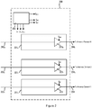
- FIG. 1 shows a typical column antenna 101 for use in mobile communication systems.
- the column antenna 101 comprises a plurality of antenna elements 103 1 to 103 N that are connected by means of a fixed or passive tapering network 105.
- the tapering network 105 is fed from a transmitter 107.
- the transmitter 107 comprises a power amplifier 109 that receives a signal that is to be transmitted from a transmitter processing circuit 111, which in turn receives the signal to be transmitted from base band processing unit 113.
- the power amplifier is biased by a bias control circuit 117, which is supplied by a fixed DC voltage 119.
- the function of the tapering network 105 is to feed each antenna element 103 1 to 103 N with the same or different amplitudes and/or phases in order to shape the combined antenna beam that is emitted by the column antenna 101.
- a disadvantage of using such a tapering function in a column antenna 101 is that energy losses will occur in the passive components and transmission lines that constitute the tapering network 105, thus degrading power efficiency.
- a further disadvantage is that the tapering function of the passive tapering network 105 is fixed, which does not therefore allow individual amplitude settings per antenna element to be changed during runtime without decreasing power efficiency, particularly over wide power ranges.
- Y et another disadvantage is that, when adjusting the phases for each antenna element in traditional antenna systems, analogue phase shifting circuits are required. Such analogue phase shifting circuits tend to be inaccurate, and it is therefore difficult to ascertain how accurate the output signal correlates to a desired value.
- US 6871049 B2 (COGNIO INC [US]) describes a method for optimizing the efficiency of each of a plurality of power amplifiers that amplify a corresponding one of a plurality of radio frequency signals for transmission by a corresponding one of a plurality of antennas.
- an apparatus for feeding an antenna array comprising at least first and second antenna elements.
- the apparatus comprises a first transmitting element configured to receive a first base band signal and to feed a first feed signal to the first antenna element, the first transmitting element comprising a first power amplifier.
- the apparatus also comprises a second transmitting element configured to receive a second base band signal and to feed a second feed signal to the second antenna element, the second transmitting element comprising a second power amplifier.
- the apparatus also comprises a tapering control unit adapted to provide a tapering function between the first feed signal to the first antenna element and the second feed signal to the second antenna element.
- the tapering control unit is adapted to provide first and second control signals for individually controlling bias settings of the first power amplifier and the second power amplifier, respectively.
- the bias setting is controlled according to the tapering function provided between the first and second feed signals.
- the controlling of the bias setting comprises controlling a supply voltage provided to the first power amplifier and the second power amplifier to fit a power capability need created by the tapering function.
- a method of providing a tapering function in an antenna array (207) comprising at least first and second antenna elements (207 1 , 207 2 ).
- the method comprises the steps of: amplifying a first base band signal using a first transmitting element comprising a first power amplifier, to provide a first feed signal for a first antenna element; amplifying a second base band signal using a second transmitting element comprising a second power amplifier, to provide a second feed signal for a second antenna element; and providing a tapering function between the first feed signal to the first antenna element and the second feed signal to the second antenna element.
- the method further comprises the steps of: adding a first calibration signal to the first base band signal and a second calibration signal to the second base band signal during a calibration mode of operation; receiving a first feedback signal from the output of the first power amplifier and a second feedback signal from the output of the second power amplifier during the calibration model; and then comparing the first and second feedback signals with the first and second wanted signals, during the calibration mode of operation; and regulating the bias settings of the first and second power amplifiers based on the comparison of the first and second feedback signals with the first and second wanted signals.
- each antenna element may itself comprise an antenna sub-array comprising a plurality of individual antenna elements.
- FIG. 2 schematically illustrates an apparatus 200 according to an embodiment of the present invention, for feeding an antenna array comprising at least first and second antenna elements (not shown).
- a first transmitting element (201 1 ) comprises a first power amplifier (203 1 ), and is configured to receive a first base band signal 202 1 , and feed a first feed signal 204 1 to a first antenna element (not shown).
- a second transmitting element (201 2 ) comprises a second power amplifier (203 2 ), and is configured to receive a second base band signal 202 2 , and feed a second feed signal 204 2 to a second antenna element (not shown).
- a tapering control unit 205 is adapted to provide a tapering function between the first feed signal to the first antenna element and the second feed signal to the second antenna element.
- the embodiment of Figure 2 has the advantage of enabling any tapering function to be provided between the first feed signal and the second feed signal.
- the tapering function may be configured according to a particular application of an antenna array, and may be configured for one type of tapering function and/or dynamically configured during use, for example when the apparatus is required to perform a different tapering function.
- the tapering control unit 205 may be adapted to provide first and second control signals S B1 , S B2 for individually controlling bias settings of the first power amplifier 203 1 and the second power amplifier 203 2 , respectively, according to the tapering function provided between the first feed signal to the first antenna element and the second feed signal to the second antenna element.
- the controlling of the bias settings may comprise controlling the supply voltage provided to a power amplifier 203, such that the power supply fits the power capability need created by the tapering function.
- a high power capability requires a high supply voltage, and vice versa.
- the bias settings of a power amplifier can be adaptively controlled to match the particular needs of a particular tapering function, thereby having the advantage of improved power efficiency.
- the tapering control unit 205 may be adapted to control a tapering function by controlling signals at the base band level. This may comprise providing a first multiplier unit (not shown) in the path of the first base band signal 202 1 and a second multiplier unit (not shown) in the path of the second base band signal 202 2 , wherein the first multiplier unit and the second multiplier unit are controlled by the tapering control unit 205, and configured to adjust the amplitude and/or phase of the first base band signal 202 1 and the second base band signal 202 2 , respectively, to provide the required tapering function between the first feed signal 204 1 to the first antenna element and the second feed signal 204 2 to the second antenna element.
- the tapering function may be created at a base band level which couples a stream of user data to the first and second transmitting elements 201 1 , 201 2 .
- the tapering function may be provided by multiplying a stream of user data by different weighted values, for example.
- the tapering function may involve adjusting the amplitude and/or phase characteristics of the feed signal for a given antenna element.
- the apparatus 200 may comprise more than first and second transmitting elements.
- the apparatus 200 may comprises N transmitting elements 201 1 to 201 N for feeding a feed signal to each of N antenna elements (not shown), where N is greater than or equal to two.
- Such an apparatus 200 also comprises a tapering control unit 205 that is arranged to provide N control signals S B1 to S BN for each of the N transmitting elements 201 1 to 201 N .
- the N transmitting elements 201 1 to 201 N each comprise a power amplifier 203 1 to 203 N .
- the tapering control unit 205 is adapted to provide at least first and second control signals S B1 to S BN to control the bias settings of the respective power amplifiers 203 1 to 203 N according to the tapering function that is being provided between the feed signals sent to the N antenna elements, thereby optimizing the efficiency of each power amplifier based on the tapering function created at base band.
- the adjustment of the bias level lowers the supply power to the power amplifier based on the output power capability required from the power amplifier, thus increasing power efficiency.
- the power capability of the power amplifier can be regulated between a maximum and a minimum value.
- the power amplifier requires more power supply, and vice versa.
- the embodiment of Figure 2 also has the advantage of enabling a tapering function to be adjusted dynamically during use, and the bias levels of each power amplifier controlled dynamically according to a particular tapering function, in order to obtain optimum efficiency in the power amplifiers.
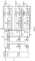
- Figure 3 schematically illustrates an apparatus according to another embodiment of the present invention.
- Figure 3 illustrates an apparatus for feeding an antenna array comprising N antenna elements 207 1 to 207 N , where N is greater than or equal to two.
- the apparatus comprises N transmitting elements 201 1 to 201 N coupled to receive base band signals 202 1 to 202 N from a base band processing circuit 213, and for feeding feed signals 204 1 to 204 N to the respective N antenna elements 207 1 to 207 N .
- the apparatus also comprises a tapering control unit 205, for providing control signals S B1 to S BN for each of the N transmitting elements 201 1 to 201 N in order to control the bias settings of respective power amplifiers according to a tapering function created as base band between the N antenna elements.
- a tapering control unit 205 for providing control signals S B1 to S BN for each of the N transmitting elements 201 1 to 201 N in order to control the bias settings of respective power amplifiers according to a tapering function created as base band between the N antenna elements.
- the tapering control unit 205 is connected to a system control and operations, administration and maintenance (OAM) unit 215.
- OAM operations, administration and maintenance
- the tapering control unit 205 which controls the N transmitting elements 201 1 to 201 N , is in turn controlled by one or more signals received from the OAM system, which may be an OAM system of a mobile communications system.
- Each transmitting element 201 1 to 201 N is therefore coupled to receive a respective signal flow (or stream of user data) from a base band processing block 213 (referred to as the base band signals 202 1 to 202 N ), and arranged to provide an input signal, (referred to as the feed signal 204 1 to 204 N ) for each respective transmitting element.
- a tapering function is therefore provided between the feed signals for the respective transmitting elements, by introducing a tapering function at base band.
- multiplier units 210 1 to 210 N can be provided in the path of the base band signals 202 1 to 202 N , for introducing the tapering coefficients corresponding to phase and/or amplitude that are needed to provide the required tapering function.
- the multiplier units 210 1 to 210 N are controlled by control signals 212 1 to 212 N received from the tapering control unit 205.
- Each transmitting element 201 1 to 201 N comprises a transmitting processor 209 1 to 209 N , which receives a base band signal 202 1 to 202 N from the base band processing block 213.
- Each transmitting processor 209 1 to 209 N up-converts the respective base band signal 202 1 to 202 N received from the base band processing block 213 to RF level, for transmission to the antenna elements 207 1 to 207 N .
- Each transmitting element 201 1 to 201 N comprises an RF power amplifier (PA), 203 1 to 203 N .
- the RF power amplifiers 203 1 to 203 N are arranged to amplify the signals from the transmitting processors 209 1 to 209 N that have been up-converted to RF level, to a required RF output level.
- the operating point and maximum power capability of the RF power amplifiers 203 1 to 203 N can be individually controlled by changing bias settings of the power amplifiers 203 1 to 203 N , according to a tapering function provided between the feed signals 204 1 to 204 N to the antenna elements 207 1 to 207 N , thus providing optimal RF energy efficiency.
- the bias settings of the power amplifiers 203 1 to 203 N are controlled by a respective biasing unit 211 1 to 211 N , each biasing unit 211 1 to 211 N being controlled by control signals S B1 to S BN received from the tapering control unit 205.
- the biasing units 211 1 to 211 N are therefore arranged to control the bias settings of the power amplifiers 203 1 to 203 N based on the respective received control signals.
- Figure 3 shows separate biasing units 211 1 to 211 N being provided for controlling the bias settings of the respective power amplifiers, it is noted that an alternative embodiment may comprise one central biasing unit that is configured to provide biasing signals to each individual power amplifier. The operating point and power capability of each power amplifier is changed by changing the bias of the power amplifier transistors.
- the controlling of the bias settings may comprise controlling a supply voltage provided to a power amplifier 203 1 to 203 N , such that the power supply fits the power capability need created by the tapering function.
- a high power capability requires a high supply voltage, and vice versa.
- the bias settings of a power amplifier can be adaptively controlled to match the particular needs of a particular tapering function, thereby having the advantage of improved power efficiency.
- the tapering settings are determined by the system control and OAM unit 215 and used to create a tapering function at the base band level, under control of the tapering control unit 205 and the multiplier units 210 1 to 210 N . Furthermore, the tapering settings determined by the system control and OAM unit 215 can be converted into bias level values before being received by the tapering control unit 205. Alternatively, the bias level values may be determined by the tapering control unit 205 itself.
- the tapering control unit 205 then generates the control signals S B1 to S BN based on the bias settings such that the operating point and/or power capability of each power amplifier can be controlled according to the tapering function to be provided between the feed signals to the N antenna elements.
- the control signals S B1 to S BN are transmitted to the biasing units 211 1 to 211 N , which control the bias of each of the respective power amplifiers 203 1 to 203 N according to the control signal values
- the biasing units 211 1 to 211 N enable a stable control to be provided, and can store values corresponding to the required bias settings, which are updated periodically by the tapering control unit 205. In this manner the biasing units 211 1 to 211 N can be adapted to start from predefined fail safe default values, which are then adjusted during use according to a particular tapering function, under control of the tapering control unit 205. This has the advantage of providing a stable control, and does not depend on external signals.
- the embodiment of Figure 3 can also be adapted to operate in a calibration mode of operation. This option enables the circuit to be fine tuned to take account of the actual gains and/or phase shifts of the respective power amplifiers (and the transmission lines connecting the power amplifiers to the antenna elements), and take account of device mismatch between the different power amplifiers, or offsets caused by factors such as temperature changes.
- N adders 217 1 to 217 N may be provided in the input signal path between the base band processing block 213 and the transmitting processing units 209 1 to 209 N .
- the N adders 217 1 to 217 N are shown as being coupled between the multiplier units 210 1 to 210 N and the transmitting processors 209 1 to 209 N .
- the N adders 217 1 to 217 N may be provided between the base band processing unit 213 and the multiplier units 210 1 to 210 N .
- the adders 217 1 to 217 N may be arranged to add a calibration signal 219 1 to 219 N to the signals from the multiplier units 210 1 to 210 N or base band processing unit 213, to provide base band signals 202 1 to 202 N to the transmitting elements 201 1 to 201 N .
- the calibration signals 219 1 to 219 N are generated by the tapering control unit 205.
- the calibration signals are added to the base band signals in order to calibrate the system during runtime so that the tapering function can be continuously calibrated.
- carrying out the calibration during runtime has the advantage of enabling parameters that change over time to be tracked during runtime (whereas the "off-line" calibration mode has the disadvantage of blocking a signalling path involved in the calibration operation).
- feedback signals F 1 to F N are provided from the transmitting elements 201 1 to 201 N to the tapering control unit 205.
- the feedback signals are provided from a coupler downstream of the output of the power amplifiers 203 1 to 203 N . It should be noted that the feedback signals may, or may not be coupled directly from the output of the power amplifiers 203 1 to 203 N .
- Each of the feedback signals is input into the tapering control unit 205.
- the feedback signals F 1 to F N are compared with the input feed signals that are input into the transmitting elements during the calibration mode, i.e. the input feed signals that include calibration signals, in order to regulate the power amplifiers 203 1 to 203 N .
- the regulating of the power amplifiers 203 1 to 203 N may comprise regulating the gain values of the power amplifiers.
- the calibration signals can be used to control the transmitter gain and/or a phase response. The response is controlled at base band.
- the power amplifier gain/phase response is however dependant on the bias settings, and thus there is a need for fine tuning control to be provided by the calibration as the bias settings are controlled from a tapering perspective.
- the calibration signals 219 1 to 219 N can be used to determine a difference between a wanted signal and an observed signal, which is then used as an error signal in the closed loop algorithm for regulation of the transmitter gain and/or phase response.
- transmitter includes the complete transmitting function, including the power amplifier, possible passive components such as an isolator, coupler or transmit filter, plus transmission lines for interconnecting these devices and their interconnection to the antenna elements.
- the calibration signals 219 1 to 219 N which are known or predetermined calibration signals, may be inserted in runtime into the signal flow by means of the adder blocks 217 1 to 217 N in order to regulate the transmitter gain and/or phase response.
- the calibration signal and feedback loop need not be provided.
- phase adjustment can be performed on the base band signal for each of the N transmitter chains of for the N antenna elements 207 1 to 207 N .
- the phase adjustment is provided as part of the required tapering function.
- FIG. 4 schematically shows further details of the tapering control unit 205 according to an embodiment of the invention.
- the tapering control unit 205 comprises a processing unit 401 that is coupled to receive control signals 402 from an OAM unit (not shown).
- the processing unit 401 is adapted to pass control signals to a tapering section 403 that is arranged to generate the control signals S B1 to S BN that provide the bias control of the transmitting units 201 1 to 201 N .
- the control signals are provided for individually controlling the bias settings, such as the bias levels of the power amplifier 203 1 to 203 N , according to a tapering function provided between the feed signals to the antenna elements 207 1 to 207 N .
- the control signals S B1 to S BN are therefore determined based on the tapering settings as determined by the system control and OAM unit 215, as described above, and received by the processing unit 401 within the tapering control unit 205.
- the processing unit 401 may also be arranged to generate the calibration signals 407 for each of the N antenna elements.
- the calibration signals may be known calibration signals.
- Figure 4 only shows a single output path 407 for transmitting the calibration signals to the N adder units of Figure 3 , it should be appreciated that there may be N calibration signal paths, one for each of the N transmitting units 201 1 to 201 N .
- the processing unit 401 may also be arranged to generate the tapering coefficients 408 for each of the N multiplier units.
- Figure 4 only shows a single output path 408 for transmitting the tapering coefficients to the N multiplier units of Figure 3 , it should be appreciated that there may be N tapering coefficient signal paths, one for each of the N multiplier units 210 1 to 210 N (these corresponding to the signals 212 1 to 212 N of Figure 3 , or the signals S T1 to S TN of Figure 2 ).
- the tapering control unit 205 further comprises a comparing section 405 that is arranged to compare the feedback signals F 1 to F N , received from the transmitting units 201 1 to 201 N , as described above, to determine how the observed signals from each transmitting element compare with wanted signals for a given set of control signals S B1 to S BN .
- the result of this comparison 409 is fed into the processing unit 401, which can then be used to regulate the power amplifiers accordingly.
- the result of the comparison can be used to regulate the gain and/or phase of the transmitters.
- the known calibration signals 407 and the feedback signals F 1 to F N can be used to adjust gain/phase values to take into account the true gain and true circuit parameters or characteristics of each power amplifier.
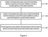
- Figure 5 shows a flow chart illustrating a method according to an embodiment of the preset invention.
- the method comprises, in step 501 amplifying a first base band signal using a first transmitting element comprising a first power amplifier to provide a first feed signal for a first antenna element.
- step 503 a second base band signal amplified using a second transmitting element comprising a second power amplifier to provide a second feed signal to a second antenna element.
- a tapering function is provided between the first feed signal to the first antenna element and the second feed signal to the second antenna element.
- step 601 the bias settings of the first and second power amplifiers are individually controlled according to a tapering function provided between the first feed signal to the first antenna element and the second feed signal to the second antenna element, as described above.
- the tapering function between the first and second antenna elements may be created at baseband level.
- Optional steps 603 to 609 may also be provided if it is desired to use a calibration signal to minimise errors in the observed output of the power amplifiers, for given bias levels of the power amplifiers.
- Step 603 comprises adding a first calibration signal to the first base band signal and a second calibration signal to the second base band signal during a calibration mode of operation.
- Step 605 comprises receiving a first feedback signal from the output of the first power amplifier and a second feedback signal from the output of the second power amplifier during the calibration mode
- Step 607 comprises comparing the first and second feedback signals with the first and second wanted signals.
- Step 609 comprises regulating the first and second power amplifiers, for example changing the bias settings of the first and second power amplifiers and/or adjusting gain values, based on the comparison of the first and second feedback signals with the first and second wanted signals.
- N antenna elements may be provided with a corresponding number of N steps for each of the N antenna elements and a tapering function provided between the N antenna elements, where N is greater than or equal to two.
- Embodiments of the invention describe an apparatus and method to implement an active antenna with integrated power amplifiers provided for each antenna element in order to achieve a flexible amplitude and/or phase tapering of the antenna elements without affecting dynamic performance, linearity and energy efficiency.
- phase adjustment either static or semi-static, can be achieved on base band signals on a per user equipment basis, that is whereby different user equipment can be configured in a simple manner to have different tapering functions.
- the power dissipation and the RF output power capability from the RF power transistor is controlled by means of a bias control.
- the RF power output capability and the power dissipation for the transistor can thus be controlled by changing the bias point of the power amplifiers.
- each power amplifier Due to this individual control of each power amplifier it is also possible to set an arbitrary tapering function. It is also possible to regulate the overall RF output power capability from P min - P max without affecting the tapering function or the RF power efficiency.
- the power amplifier output power capability and power efficiency is controlled by means of adjusting the bias setting. Thus, if the power capability of a power amplifier is adjusted between P min - P max , the power amplifier bias is adjusted to accommodate the new capability setting without affecting the tapering function or the RF power efficiency.
- a particular antenna tapering function can be set up at equipment deployment.
- a column antenna can be set up for a given application, and thereafter operated in this mode of operation.
- the antenna tapering can be dynamically changed during runtime in order to follow for example traffic changes, rearrangement of cell structure. This involves changing the control signals S B1 to S BN (and/or S T1 to S TN ) in dependence on signals from the system control and OAM unit 215, to thereby take account of traffic changes, cell restructure, or other considerations, such that the bias settings are adjusted to reflect a particular tapering function between the separate antenna elements.
- Embodiments of the present invention have the advantage of providing flexible tapering whilst maintaining power efficiency. Embodiments of the present invention also have the advantage of not requiring antennas to be exchanged when new antenna patterns are required.
- the tapering can be changed in runtime based on for example traffic changes or cell rearrangement. This enables antenna performance to be optimized due to traffic situation and network status.
- the tapering can be set at deployment of the infrastructure, rather than at the time of manufacture. This enables the tapering to be tailored to the requirements of the system in situ.
- embodiments of the present invention can achieve new antenna beam patterns by applying tapering to parts or the whole matrix antenna elements.
- Embodiments of the present invention allow overall RF power regulation to be used by controlling the tapering of the antenna elements in order to maintain overall system efficiency, as the required RF power is a function of traffic demands.
- each antenna element may be an individual antenna element, or a combination of two or more antenna elements organised into a sub-group of antenna elements.
- controlling of the bias settings may also comprise controlling the gate bias of a power amplifier 203, for controlling the gain of the power amplifier.
- the gain of a power amplifier may also be controlled by an embedded function such as digital pre-distortion or by a calibration process as described above.
Landscapes
- Engineering & Computer Science (AREA)
- Power Engineering (AREA)
- Computer Networks & Wireless Communication (AREA)
- Signal Processing (AREA)
- Transmitters (AREA)
- Amplifiers (AREA)
- Variable-Direction Aerials And Aerial Arrays (AREA)
Applications Claiming Priority (1)
| Application Number | Priority Date | Filing Date | Title |
|---|---|---|---|
| PCT/EP2011/067607 WO2013050085A1 (en) | 2011-10-07 | 2011-10-07 | Apparatus and method for use with antenna array |
Publications (2)
| Publication Number | Publication Date |
|---|---|
| EP2756549A1 EP2756549A1 (en) | 2014-07-23 |
| EP2756549B1 true EP2756549B1 (en) | 2018-09-26 |
Family
ID=44759720
Family Applications (1)
| Application Number | Title | Priority Date | Filing Date |
|---|---|---|---|
| EP11764793.3A Not-in-force EP2756549B1 (en) | 2011-10-07 | 2011-10-07 | Apparatus and method for use with antenna array |
Country Status (4)
| Country | Link |
|---|---|
| US (1) | US9712191B2 (enExample) |
| EP (1) | EP2756549B1 (enExample) |
| IN (1) | IN2014KN00955A (enExample) |
| WO (1) | WO2013050085A1 (enExample) |
Cited By (1)
| Publication number | Priority date | Publication date | Assignee | Title |
|---|---|---|---|---|
| WO2025198960A1 (en) * | 2024-03-20 | 2025-09-25 | Qualcomm Incorporated | Area-efficient power detection subsystem for phased array transmitter |
Families Citing this family (9)
| Publication number | Priority date | Publication date | Assignee | Title |
|---|---|---|---|---|
| US10484106B2 (en) * | 2016-05-05 | 2019-11-19 | International Business Machines Corporation | Antenna calibration |
| US10187019B1 (en) * | 2018-03-26 | 2019-01-22 | Qorvo Us, Inc. | Phased array antenna system |
| US10897162B2 (en) * | 2019-04-12 | 2021-01-19 | Psemi Corporation | Antenna array element by element power tracking |
| US11495890B2 (en) * | 2020-05-08 | 2022-11-08 | Qualcomm Incorporated | Power amplifier control with an antenna array |
| KR20210152860A (ko) * | 2020-06-09 | 2021-12-16 | 삼성전자주식회사 | 복수의 증폭기를 이용한 신호의 증폭을 수행하는 통신 회로와 그것을 구비한 전자 장치 |
| US12347938B2 (en) | 2021-02-11 | 2025-07-01 | Saab Ab | Method and device for controlling the output efficiency of a plurality of amplifiers |
| US12160267B2 (en) | 2021-05-26 | 2024-12-03 | Corning Research & Development Corporation | Dynamic radio frequency (RF) beam pattern adaptation in a wireless communications system (WCS) |
| US11159958B1 (en) | 2021-06-08 | 2021-10-26 | Peltbeam Inc. | Central cloud server and edge devices assisted high speed low-latency wireless connectivity |
| US11606070B1 (en) * | 2021-09-09 | 2023-03-14 | Qualcomm Incorporated | Radio frequency (RF) signal power detector using different power rails to receive currents from which power-indicating voltage is generated |
Citations (1)
| Publication number | Priority date | Publication date | Assignee | Title |
|---|---|---|---|---|
| US6871049B2 (en) * | 2002-03-21 | 2005-03-22 | Cognio, Inc. | Improving the efficiency of power amplifiers in devices using transmit beamforming |
Family Cites Families (14)
| Publication number | Priority date | Publication date | Assignee | Title |
|---|---|---|---|---|
| US6157343A (en) * | 1996-09-09 | 2000-12-05 | Telefonaktiebolaget Lm Ericsson | Antenna array calibration |
| BR9507801A (pt) * | 1994-06-03 | 1998-05-26 | Ericsson Telefon Ab L M | Processo e sistema para calibrar a transmissão e a recepção de uma formação de antenas para uso num sistema de comunicações de rádio móvel |
| US6091934A (en) * | 1997-09-02 | 2000-07-18 | Hughes Electronics Corporation | Dynamic power allocation system and method for multi-beam satellite amplifiers |
| US6684064B2 (en) * | 2000-03-29 | 2004-01-27 | Interdigital Technology Corp. | Dynamic bias for RF power amplifiers |
| US7013165B2 (en) * | 2000-08-16 | 2006-03-14 | Samsung Electronics Co., Ltd. | Antenna array apparatus and beamforming method using GPS signal for base station in mobile telecommunication system |
| US6646600B2 (en) * | 2001-11-09 | 2003-11-11 | Harris Corporation | Phased array antenna with controllable amplifier bias adjustment and related methods |
| JP2003218621A (ja) * | 2002-01-21 | 2003-07-31 | Nec Corp | アレーアンテナの校正装置及び校正方法 |
| AU2003220200A1 (en) * | 2002-03-21 | 2003-10-08 | Cognio, Inc. | Improving the efficiency of power amplifiers in devices using transmit beamforming |
| JP4209355B2 (ja) * | 2004-03-30 | 2009-01-14 | 富士通株式会社 | 位相キャリブレーション方法及び位相キャリブレーション装置 |
| JP2006005525A (ja) * | 2004-06-16 | 2006-01-05 | Nec Corp | 送信装置 |
| JP4478606B2 (ja) * | 2005-05-19 | 2010-06-09 | 富士通株式会社 | リニアアレイアンテナの校正装置及び校正方法 |
| JP4528208B2 (ja) * | 2005-06-10 | 2010-08-18 | 富士通株式会社 | アレイアンテナの校正装置及び校正方法 |
| JP5022792B2 (ja) * | 2007-07-02 | 2012-09-12 | 株式会社日立国際電気 | Dcdcコンバータユニット、電力増幅器、及び基地局装置 |
| US9397396B2 (en) | 2009-04-01 | 2016-07-19 | Kathrein-Werke Kg | Radio system and a method for relaying packetized radio signals |
-
2011
- 2011-10-07 EP EP11764793.3A patent/EP2756549B1/en not_active Not-in-force
- 2011-10-07 WO PCT/EP2011/067607 patent/WO2013050085A1/en not_active Ceased
- 2011-10-07 US US14/348,937 patent/US9712191B2/en active Active
- 2011-10-07 IN IN955KON2014 patent/IN2014KN00955A/en unknown
Patent Citations (1)
| Publication number | Priority date | Publication date | Assignee | Title |
|---|---|---|---|---|
| US6871049B2 (en) * | 2002-03-21 | 2005-03-22 | Cognio, Inc. | Improving the efficiency of power amplifiers in devices using transmit beamforming |
Cited By (1)
| Publication number | Priority date | Publication date | Assignee | Title |
|---|---|---|---|---|
| WO2025198960A1 (en) * | 2024-03-20 | 2025-09-25 | Qualcomm Incorporated | Area-efficient power detection subsystem for phased array transmitter |
Also Published As
| Publication number | Publication date |
|---|---|
| EP2756549A1 (en) | 2014-07-23 |
| US9712191B2 (en) | 2017-07-18 |
| IN2014KN00955A (enExample) | 2015-10-09 |
| WO2013050085A1 (en) | 2013-04-11 |
| US20140248843A1 (en) | 2014-09-04 |
Similar Documents
| Publication | Publication Date | Title |
|---|---|---|
| EP2756549B1 (en) | Apparatus and method for use with antenna array | |
| CN109565293B (zh) | 用于多天线系统的数字预失真 | |
| US10396845B2 (en) | Split microwave backhaul transceiver architecture with coaxial interconnect | |
| US6871049B2 (en) | Improving the efficiency of power amplifiers in devices using transmit beamforming | |
| KR101433845B1 (ko) | 다중 안테나 무선통신 시스템에서 피드백 경로를 공유하는디지털 선 왜곡 장치 및 방법 | |
| EP3267579B1 (en) | Linearizing power amplifiers outputs in multi-antenna system | |
| EP2128997B1 (en) | Distortion compensating apparatus, wireless communication apparatus, and distortion compensating method | |
| KR101118919B1 (ko) | 송수신모듈을 내장한 기지국 안테나장치 | |
| CN108512612B (zh) | 发射和接收校准装置、系统及方法 | |
| US11075606B2 (en) | Power amplifier circuit and antenna device | |
| US8571497B1 (en) | Closed-loop power control in conjunction with adaptive power amplifier linearization | |
| JP7622756B2 (ja) | 信号処理装置、信号処理方法及びプログラム | |
| CA2937064A1 (en) | Multi-channel array distortion compensation apparatus and method | |
| US11171613B1 (en) | Methods and apparatus for using signal pre-distortion with individual power amplifier (PA) control | |
| US11005517B2 (en) | Handling of unwanted emissions from a radio communications device | |
| KR102019082B1 (ko) | 밀리미터파 빔포밍을 위한 4채널 위상 정밀 제어 장치 | |
| EP1595329A2 (en) | Improving the efficiency of power amplifiers in devices using transmit beamforming | |
| US20180138867A1 (en) | Base station and distortion compensation method | |
| CN107425897A (zh) | 环路增益控制系统和方法 | |
| US8396420B2 (en) | Active antenna system for a mobile communications network as well as a method for relaying a plurality of radio signals through the active antenna system | |
| JP6219007B1 (ja) | フィードフォワード増幅器及びアンテナ装置 | |
| JP7619437B2 (ja) | 信号処理装置、無線通信装置、信号処理方法及びプログラム | |
| EP4540923A1 (en) | Antenna array power amplifier mismatch mitigation | |
| JP2004179943A (ja) | 無線送信装置および無線送信方法 | |
| WO2018105147A1 (ja) | アレイアンテナシステム |
Legal Events
| Date | Code | Title | Description |
|---|---|---|---|
| PUAI | Public reference made under article 153(3) epc to a published international application that has entered the european phase |
Free format text: ORIGINAL CODE: 0009012 |
|
| 17P | Request for examination filed |
Effective date: 20140327 |
|
| AK | Designated contracting states |
Kind code of ref document: A1 Designated state(s): AL AT BE BG CH CY CZ DE DK EE ES FI FR GB GR HR HU IE IS IT LI LT LU LV MC MK MT NL NO PL PT RO RS SE SI SK SM TR |
|
| DAX | Request for extension of the european patent (deleted) | ||
| STAA | Information on the status of an ep patent application or granted ep patent |
Free format text: STATUS: EXAMINATION IS IN PROGRESS |
|
| 17Q | First examination report despatched |
Effective date: 20171128 |
|
| GRAP | Despatch of communication of intention to grant a patent |
Free format text: ORIGINAL CODE: EPIDOSNIGR1 |
|
| STAA | Information on the status of an ep patent application or granted ep patent |
Free format text: STATUS: GRANT OF PATENT IS INTENDED |
|
| INTG | Intention to grant announced |
Effective date: 20180629 |
|
| GRAS | Grant fee paid |
Free format text: ORIGINAL CODE: EPIDOSNIGR3 |
|
| GRAA | (expected) grant |
Free format text: ORIGINAL CODE: 0009210 |
|
| STAA | Information on the status of an ep patent application or granted ep patent |
Free format text: STATUS: THE PATENT HAS BEEN GRANTED |
|
| AK | Designated contracting states |
Kind code of ref document: B1 Designated state(s): AL AT BE BG CH CY CZ DE DK EE ES FI FR GB GR HR HU IE IS IT LI LT LU LV MC MK MT NL NO PL PT RO RS SE SI SK SM TR |
|
| REG | Reference to a national code |
Ref country code: GB Ref legal event code: FG4D |
|
| REG | Reference to a national code |
Ref country code: CH Ref legal event code: EP |
|
| REG | Reference to a national code |
Ref country code: AT Ref legal event code: REF Ref document number: 1047116 Country of ref document: AT Kind code of ref document: T Effective date: 20181015 |
|
| REG | Reference to a national code |
Ref country code: IE Ref legal event code: FG4D |
|
| REG | Reference to a national code |
Ref country code: DE Ref legal event code: R096 Ref document number: 602011052378 Country of ref document: DE |
|
| REG | Reference to a national code |
Ref country code: NL Ref legal event code: MP Effective date: 20180926 |
|
| PG25 | Lapsed in a contracting state [announced via postgrant information from national office to epo] |
Ref country code: LT Free format text: LAPSE BECAUSE OF FAILURE TO SUBMIT A TRANSLATION OF THE DESCRIPTION OR TO PAY THE FEE WITHIN THE PRESCRIBED TIME-LIMIT Effective date: 20180926 Ref country code: NO Free format text: LAPSE BECAUSE OF FAILURE TO SUBMIT A TRANSLATION OF THE DESCRIPTION OR TO PAY THE FEE WITHIN THE PRESCRIBED TIME-LIMIT Effective date: 20181226 Ref country code: GR Free format text: LAPSE BECAUSE OF FAILURE TO SUBMIT A TRANSLATION OF THE DESCRIPTION OR TO PAY THE FEE WITHIN THE PRESCRIBED TIME-LIMIT Effective date: 20181227 Ref country code: BG Free format text: LAPSE BECAUSE OF FAILURE TO SUBMIT A TRANSLATION OF THE DESCRIPTION OR TO PAY THE FEE WITHIN THE PRESCRIBED TIME-LIMIT Effective date: 20181226 Ref country code: SE Free format text: LAPSE BECAUSE OF FAILURE TO SUBMIT A TRANSLATION OF THE DESCRIPTION OR TO PAY THE FEE WITHIN THE PRESCRIBED TIME-LIMIT Effective date: 20180926 Ref country code: RS Free format text: LAPSE BECAUSE OF FAILURE TO SUBMIT A TRANSLATION OF THE DESCRIPTION OR TO PAY THE FEE WITHIN THE PRESCRIBED TIME-LIMIT Effective date: 20180926 Ref country code: FI Free format text: LAPSE BECAUSE OF FAILURE TO SUBMIT A TRANSLATION OF THE DESCRIPTION OR TO PAY THE FEE WITHIN THE PRESCRIBED TIME-LIMIT Effective date: 20180926 |
|
| REG | Reference to a national code |
Ref country code: LT Ref legal event code: MG4D |
|
| PG25 | Lapsed in a contracting state [announced via postgrant information from national office to epo] |
Ref country code: HR Free format text: LAPSE BECAUSE OF FAILURE TO SUBMIT A TRANSLATION OF THE DESCRIPTION OR TO PAY THE FEE WITHIN THE PRESCRIBED TIME-LIMIT Effective date: 20180926 Ref country code: AL Free format text: LAPSE BECAUSE OF FAILURE TO SUBMIT A TRANSLATION OF THE DESCRIPTION OR TO PAY THE FEE WITHIN THE PRESCRIBED TIME-LIMIT Effective date: 20180926 Ref country code: LV Free format text: LAPSE BECAUSE OF FAILURE TO SUBMIT A TRANSLATION OF THE DESCRIPTION OR TO PAY THE FEE WITHIN THE PRESCRIBED TIME-LIMIT Effective date: 20180926 |
|
| PGFP | Annual fee paid to national office [announced via postgrant information from national office to epo] |
Ref country code: GB Payment date: 20181029 Year of fee payment: 8 |
|
| REG | Reference to a national code |
Ref country code: AT Ref legal event code: MK05 Ref document number: 1047116 Country of ref document: AT Kind code of ref document: T Effective date: 20180926 |
|
| PG25 | Lapsed in a contracting state [announced via postgrant information from national office to epo] |
Ref country code: IS Free format text: LAPSE BECAUSE OF FAILURE TO SUBMIT A TRANSLATION OF THE DESCRIPTION OR TO PAY THE FEE WITHIN THE PRESCRIBED TIME-LIMIT Effective date: 20190126 Ref country code: AT Free format text: LAPSE BECAUSE OF FAILURE TO SUBMIT A TRANSLATION OF THE DESCRIPTION OR TO PAY THE FEE WITHIN THE PRESCRIBED TIME-LIMIT Effective date: 20180926 Ref country code: IT Free format text: LAPSE BECAUSE OF FAILURE TO SUBMIT A TRANSLATION OF THE DESCRIPTION OR TO PAY THE FEE WITHIN THE PRESCRIBED TIME-LIMIT Effective date: 20180926 Ref country code: EE Free format text: LAPSE BECAUSE OF FAILURE TO SUBMIT A TRANSLATION OF THE DESCRIPTION OR TO PAY THE FEE WITHIN THE PRESCRIBED TIME-LIMIT Effective date: 20180926 Ref country code: CZ Free format text: LAPSE BECAUSE OF FAILURE TO SUBMIT A TRANSLATION OF THE DESCRIPTION OR TO PAY THE FEE WITHIN THE PRESCRIBED TIME-LIMIT Effective date: 20180926 Ref country code: RO Free format text: LAPSE BECAUSE OF FAILURE TO SUBMIT A TRANSLATION OF THE DESCRIPTION OR TO PAY THE FEE WITHIN THE PRESCRIBED TIME-LIMIT Effective date: 20180926 Ref country code: NL Free format text: LAPSE BECAUSE OF FAILURE TO SUBMIT A TRANSLATION OF THE DESCRIPTION OR TO PAY THE FEE WITHIN THE PRESCRIBED TIME-LIMIT Effective date: 20180926 Ref country code: PL Free format text: LAPSE BECAUSE OF FAILURE TO SUBMIT A TRANSLATION OF THE DESCRIPTION OR TO PAY THE FEE WITHIN THE PRESCRIBED TIME-LIMIT Effective date: 20180926 Ref country code: ES Free format text: LAPSE BECAUSE OF FAILURE TO SUBMIT A TRANSLATION OF THE DESCRIPTION OR TO PAY THE FEE WITHIN THE PRESCRIBED TIME-LIMIT Effective date: 20180926 |
|
| PG25 | Lapsed in a contracting state [announced via postgrant information from national office to epo] |
Ref country code: PT Free format text: LAPSE BECAUSE OF FAILURE TO SUBMIT A TRANSLATION OF THE DESCRIPTION OR TO PAY THE FEE WITHIN THE PRESCRIBED TIME-LIMIT Effective date: 20190126 Ref country code: SK Free format text: LAPSE BECAUSE OF FAILURE TO SUBMIT A TRANSLATION OF THE DESCRIPTION OR TO PAY THE FEE WITHIN THE PRESCRIBED TIME-LIMIT Effective date: 20180926 Ref country code: SM Free format text: LAPSE BECAUSE OF FAILURE TO SUBMIT A TRANSLATION OF THE DESCRIPTION OR TO PAY THE FEE WITHIN THE PRESCRIBED TIME-LIMIT Effective date: 20180926 |
|
| REG | Reference to a national code |
Ref country code: CH Ref legal event code: PL |
|
| REG | Reference to a national code |
Ref country code: BE Ref legal event code: MM Effective date: 20181031 |
|
| REG | Reference to a national code |
Ref country code: DE Ref legal event code: R097 Ref document number: 602011052378 Country of ref document: DE |
|
| PG25 | Lapsed in a contracting state [announced via postgrant information from national office to epo] |
Ref country code: LU Free format text: LAPSE BECAUSE OF NON-PAYMENT OF DUE FEES Effective date: 20181007 |
|
| REG | Reference to a national code |
Ref country code: IE Ref legal event code: MM4A |
|
| PG25 | Lapsed in a contracting state [announced via postgrant information from national office to epo] |
Ref country code: MC Free format text: LAPSE BECAUSE OF FAILURE TO SUBMIT A TRANSLATION OF THE DESCRIPTION OR TO PAY THE FEE WITHIN THE PRESCRIBED TIME-LIMIT Effective date: 20180926 Ref country code: DK Free format text: LAPSE BECAUSE OF FAILURE TO SUBMIT A TRANSLATION OF THE DESCRIPTION OR TO PAY THE FEE WITHIN THE PRESCRIBED TIME-LIMIT Effective date: 20180926 |
|
| PLBE | No opposition filed within time limit |
Free format text: ORIGINAL CODE: 0009261 |
|
| STAA | Information on the status of an ep patent application or granted ep patent |
Free format text: STATUS: NO OPPOSITION FILED WITHIN TIME LIMIT |
|
| PG25 | Lapsed in a contracting state [announced via postgrant information from national office to epo] |
Ref country code: BE Free format text: LAPSE BECAUSE OF NON-PAYMENT OF DUE FEES Effective date: 20181031 Ref country code: LI Free format text: LAPSE BECAUSE OF NON-PAYMENT OF DUE FEES Effective date: 20181031 Ref country code: CH Free format text: LAPSE BECAUSE OF NON-PAYMENT OF DUE FEES Effective date: 20181031 |
|
| 26N | No opposition filed |
Effective date: 20190627 |
|
| PG25 | Lapsed in a contracting state [announced via postgrant information from national office to epo] |
Ref country code: SI Free format text: LAPSE BECAUSE OF FAILURE TO SUBMIT A TRANSLATION OF THE DESCRIPTION OR TO PAY THE FEE WITHIN THE PRESCRIBED TIME-LIMIT Effective date: 20180926 Ref country code: IE Free format text: LAPSE BECAUSE OF NON-PAYMENT OF DUE FEES Effective date: 20181007 Ref country code: FR Free format text: LAPSE BECAUSE OF NON-PAYMENT OF DUE FEES Effective date: 20181126 |
|
| PG25 | Lapsed in a contracting state [announced via postgrant information from national office to epo] |
Ref country code: MT Free format text: LAPSE BECAUSE OF NON-PAYMENT OF DUE FEES Effective date: 20181007 |
|
| PG25 | Lapsed in a contracting state [announced via postgrant information from national office to epo] |
Ref country code: TR Free format text: LAPSE BECAUSE OF FAILURE TO SUBMIT A TRANSLATION OF THE DESCRIPTION OR TO PAY THE FEE WITHIN THE PRESCRIBED TIME-LIMIT Effective date: 20180926 |
|
| PG25 | Lapsed in a contracting state [announced via postgrant information from national office to epo] |
Ref country code: HU Free format text: LAPSE BECAUSE OF FAILURE TO SUBMIT A TRANSLATION OF THE DESCRIPTION OR TO PAY THE FEE WITHIN THE PRESCRIBED TIME-LIMIT; INVALID AB INITIO Effective date: 20111007 Ref country code: MK Free format text: LAPSE BECAUSE OF NON-PAYMENT OF DUE FEES Effective date: 20180926 Ref country code: CY Free format text: LAPSE BECAUSE OF FAILURE TO SUBMIT A TRANSLATION OF THE DESCRIPTION OR TO PAY THE FEE WITHIN THE PRESCRIBED TIME-LIMIT Effective date: 20180926 |
|
| GBPC | Gb: european patent ceased through non-payment of renewal fee |
Effective date: 20191007 |
|
| PG25 | Lapsed in a contracting state [announced via postgrant information from national office to epo] |
Ref country code: GB Free format text: LAPSE BECAUSE OF NON-PAYMENT OF DUE FEES Effective date: 20191007 |
|
| PGFP | Annual fee paid to national office [announced via postgrant information from national office to epo] |
Ref country code: DE Payment date: 20211027 Year of fee payment: 11 |
|
| REG | Reference to a national code |
Ref country code: DE Ref legal event code: R119 Ref document number: 602011052378 Country of ref document: DE |
|
| PG25 | Lapsed in a contracting state [announced via postgrant information from national office to epo] |
Ref country code: DE Free format text: LAPSE BECAUSE OF NON-PAYMENT OF DUE FEES Effective date: 20230503 |