EP2755233A1 - Underfill composition - Google Patents
Underfill composition Download PDFInfo
- Publication number
- EP2755233A1 EP2755233A1 EP20120830373 EP12830373A EP2755233A1 EP 2755233 A1 EP2755233 A1 EP 2755233A1 EP 20120830373 EP20120830373 EP 20120830373 EP 12830373 A EP12830373 A EP 12830373A EP 2755233 A1 EP2755233 A1 EP 2755233A1
- Authority
- EP
- European Patent Office
- Prior art keywords
- composition
- compound
- composition according
- meth
- electronic device
- Prior art date
- Legal status (The legal status is an assumption and is not a legal conclusion. Google has not performed a legal analysis and makes no representation as to the accuracy of the status listed.)
- Granted
Links
- HKZXDFQIKRFLMW-UHFFFAOYSA-N CC(C)C1C=CCCC1 Chemical compound CC(C)C1C=CCCC1 HKZXDFQIKRFLMW-UHFFFAOYSA-N 0.000 description 1
Classifications
-
- C—CHEMISTRY; METALLURGY
- C08—ORGANIC MACROMOLECULAR COMPOUNDS; THEIR PREPARATION OR CHEMICAL WORKING-UP; COMPOSITIONS BASED THEREON
- C08F—MACROMOLECULAR COMPOUNDS OBTAINED BY REACTIONS ONLY INVOLVING CARBON-TO-CARBON UNSATURATED BONDS
- C08F220/00—Copolymers of compounds having one or more unsaturated aliphatic radicals, each having only one carbon-to-carbon double bond, and only one being terminated by only one carboxyl radical or a salt, anhydride ester, amide, imide or nitrile thereof
- C08F220/02—Monocarboxylic acids having less than ten carbon atoms; Derivatives thereof
- C08F220/10—Esters
- C08F220/12—Esters of monohydric alcohols or phenols
- C08F220/16—Esters of monohydric alcohols or phenols of phenols or of alcohols containing two or more carbon atoms
- C08F220/18—Esters of monohydric alcohols or phenols of phenols or of alcohols containing two or more carbon atoms with acrylic or methacrylic acids
-
- C—CHEMISTRY; METALLURGY
- C09—DYES; PAINTS; POLISHES; NATURAL RESINS; ADHESIVES; COMPOSITIONS NOT OTHERWISE PROVIDED FOR; APPLICATIONS OF MATERIALS NOT OTHERWISE PROVIDED FOR
- C09J—ADHESIVES; NON-MECHANICAL ASPECTS OF ADHESIVE PROCESSES IN GENERAL; ADHESIVE PROCESSES NOT PROVIDED FOR ELSEWHERE; USE OF MATERIALS AS ADHESIVES
- C09J133/00—Adhesives based on homopolymers or copolymers of compounds having one or more unsaturated aliphatic radicals, each having only one carbon-to-carbon double bond, and at least one being terminated by only one carboxyl radical, or of salts, anhydrides, esters, amides, imides, or nitriles thereof; Adhesives based on derivatives of such polymers
- C09J133/04—Homopolymers or copolymers of esters
- C09J133/14—Homopolymers or copolymers of esters of esters containing halogen, nitrogen, sulfur or oxygen atoms in addition to the carboxy oxygen
-
- C—CHEMISTRY; METALLURGY
- C08—ORGANIC MACROMOLECULAR COMPOUNDS; THEIR PREPARATION OR CHEMICAL WORKING-UP; COMPOSITIONS BASED THEREON
- C08F—MACROMOLECULAR COMPOUNDS OBTAINED BY REACTIONS ONLY INVOLVING CARBON-TO-CARBON UNSATURATED BONDS
- C08F222/00—Copolymers of compounds having one or more unsaturated aliphatic radicals, each having only one carbon-to-carbon double bond, and at least one being terminated by a carboxyl radical and containing at least one other carboxyl radical in the molecule; Salts, anhydrides, esters, amides, imides, or nitriles thereof
- C08F222/36—Amides or imides
- C08F222/40—Imides, e.g. cyclic imides
-
- C—CHEMISTRY; METALLURGY
- C09—DYES; PAINTS; POLISHES; NATURAL RESINS; ADHESIVES; COMPOSITIONS NOT OTHERWISE PROVIDED FOR; APPLICATIONS OF MATERIALS NOT OTHERWISE PROVIDED FOR
- C09D—COATING COMPOSITIONS, e.g. PAINTS, VARNISHES OR LACQUERS; FILLING PASTES; CHEMICAL PAINT OR INK REMOVERS; INKS; CORRECTING FLUIDS; WOODSTAINS; PASTES OR SOLIDS FOR COLOURING OR PRINTING; USE OF MATERIALS THEREFOR
- C09D135/00—Coating compositions based on homopolymers or copolymers of compounds having one or more unsaturated aliphatic radicals, each having only one carbon-to-carbon double bond, and at least one being terminated by a carboxyl radical, and containing at least another carboxyl radical in the molecule, or of salts, anhydrides, esters, amides, imides or nitriles thereof; Coating compositions based on derivatives of such polymers
-
- C—CHEMISTRY; METALLURGY
- C09—DYES; PAINTS; POLISHES; NATURAL RESINS; ADHESIVES; COMPOSITIONS NOT OTHERWISE PROVIDED FOR; APPLICATIONS OF MATERIALS NOT OTHERWISE PROVIDED FOR
- C09D—COATING COMPOSITIONS, e.g. PAINTS, VARNISHES OR LACQUERS; FILLING PASTES; CHEMICAL PAINT OR INK REMOVERS; INKS; CORRECTING FLUIDS; WOODSTAINS; PASTES OR SOLIDS FOR COLOURING OR PRINTING; USE OF MATERIALS THEREFOR
- C09D4/00—Coating compositions, e.g. paints, varnishes or lacquers, based on organic non-macromolecular compounds having at least one polymerisable carbon-to-carbon unsaturated bond ; Coating compositions, based on monomers of macromolecular compounds of groups C09D183/00 - C09D183/16
- C09D4/06—Organic non-macromolecular compounds having at least one polymerisable carbon-to-carbon unsaturated bond in combination with a macromolecular compound other than an unsaturated polymer of groups C09D159/00 - C09D187/00
-
- H—ELECTRICITY
- H10—SEMICONDUCTOR DEVICES; ELECTRIC SOLID-STATE DEVICES NOT OTHERWISE PROVIDED FOR
- H10W—GENERIC PACKAGES, INTERCONNECTIONS, CONNECTORS OR OTHER CONSTRUCTIONAL DETAILS OF DEVICES COVERED BY CLASS H10
- H10W72/00—Interconnections or connectors in packages
- H10W72/30—Die-attach connectors
-
- H—ELECTRICITY
- H10—SEMICONDUCTOR DEVICES; ELECTRIC SOLID-STATE DEVICES NOT OTHERWISE PROVIDED FOR
- H10W—GENERIC PACKAGES, INTERCONNECTIONS, CONNECTORS OR OTHER CONSTRUCTIONAL DETAILS OF DEVICES COVERED BY CLASS H10
- H10W74/00—Encapsulations, e.g. protective coatings
- H10W74/01—Manufacture or treatment
- H10W74/012—Manufacture or treatment of encapsulations on active surfaces of flip-chip devices, e.g. forming underfills
-
- H—ELECTRICITY
- H10—SEMICONDUCTOR DEVICES; ELECTRIC SOLID-STATE DEVICES NOT OTHERWISE PROVIDED FOR
- H10W—GENERIC PACKAGES, INTERCONNECTIONS, CONNECTORS OR OTHER CONSTRUCTIONAL DETAILS OF DEVICES COVERED BY CLASS H10
- H10W74/00—Encapsulations, e.g. protective coatings
- H10W74/10—Encapsulations, e.g. protective coatings characterised by their shape or disposition
-
- H—ELECTRICITY
- H10—SEMICONDUCTOR DEVICES; ELECTRIC SOLID-STATE DEVICES NOT OTHERWISE PROVIDED FOR
- H10W—GENERIC PACKAGES, INTERCONNECTIONS, CONNECTORS OR OTHER CONSTRUCTIONAL DETAILS OF DEVICES COVERED BY CLASS H10
- H10W74/00—Encapsulations, e.g. protective coatings
- H10W74/10—Encapsulations, e.g. protective coatings characterised by their shape or disposition
- H10W74/15—Encapsulations, e.g. protective coatings characterised by their shape or disposition on active surfaces of flip-chip devices, e.g. underfills
-
- H—ELECTRICITY
- H10—SEMICONDUCTOR DEVICES; ELECTRIC SOLID-STATE DEVICES NOT OTHERWISE PROVIDED FOR
- H10W—GENERIC PACKAGES, INTERCONNECTIONS, CONNECTORS OR OTHER CONSTRUCTIONAL DETAILS OF DEVICES COVERED BY CLASS H10
- H10W74/00—Encapsulations, e.g. protective coatings
- H10W74/40—Encapsulations, e.g. protective coatings characterised by their materials
- H10W74/47—Encapsulations, e.g. protective coatings characterised by their materials comprising organic materials, e.g. plastics or resins
-
- C—CHEMISTRY; METALLURGY
- C08—ORGANIC MACROMOLECULAR COMPOUNDS; THEIR PREPARATION OR CHEMICAL WORKING-UP; COMPOSITIONS BASED THEREON
- C08F—MACROMOLECULAR COMPOUNDS OBTAINED BY REACTIONS ONLY INVOLVING CARBON-TO-CARBON UNSATURATED BONDS
- C08F222/00—Copolymers of compounds having one or more unsaturated aliphatic radicals, each having only one carbon-to-carbon double bond, and at least one being terminated by a carboxyl radical and containing at least one other carboxyl radical in the molecule; Salts, anhydrides, esters, amides, imides, or nitriles thereof
- C08F222/10—Esters
- C08F222/1006—Esters of polyhydric alcohols or polyhydric phenols
- C08F222/102—Esters of polyhydric alcohols or polyhydric phenols of dialcohols, e.g. ethylene glycol di(meth)acrylate or 1,4-butanediol dimethacrylate
-
- H—ELECTRICITY
- H10—SEMICONDUCTOR DEVICES; ELECTRIC SOLID-STATE DEVICES NOT OTHERWISE PROVIDED FOR
- H10W—GENERIC PACKAGES, INTERCONNECTIONS, CONNECTORS OR OTHER CONSTRUCTIONAL DETAILS OF DEVICES COVERED BY CLASS H10
- H10W72/00—Interconnections or connectors in packages
- H10W72/30—Die-attach connectors
- H10W72/351—Materials of die-attach connectors
- H10W72/353—Materials of die-attach connectors not comprising solid metals or solid metalloids, e.g. ceramics
- H10W72/354—Materials of die-attach connectors not comprising solid metals or solid metalloids, e.g. ceramics comprising polymers
-
- H—ELECTRICITY
- H10—SEMICONDUCTOR DEVICES; ELECTRIC SOLID-STATE DEVICES NOT OTHERWISE PROVIDED FOR
- H10W—GENERIC PACKAGES, INTERCONNECTIONS, CONNECTORS OR OTHER CONSTRUCTIONAL DETAILS OF DEVICES COVERED BY CLASS H10
- H10W90/00—Package configurations
- H10W90/701—Package configurations characterised by the relative positions of pads or connectors relative to package parts
- H10W90/721—Package configurations characterised by the relative positions of pads or connectors relative to package parts of bump connectors
- H10W90/724—Package configurations characterised by the relative positions of pads or connectors relative to package parts of bump connectors between a chip and a stacked insulating package substrate, interposer or RDL
-
- H—ELECTRICITY
- H10—SEMICONDUCTOR DEVICES; ELECTRIC SOLID-STATE DEVICES NOT OTHERWISE PROVIDED FOR
- H10W—GENERIC PACKAGES, INTERCONNECTIONS, CONNECTORS OR OTHER CONSTRUCTIONAL DETAILS OF DEVICES COVERED BY CLASS H10
- H10W90/00—Package configurations
- H10W90/701—Package configurations characterised by the relative positions of pads or connectors relative to package parts
- H10W90/731—Package configurations characterised by the relative positions of pads or connectors relative to package parts of die-attach connectors
- H10W90/734—Package configurations characterised by the relative positions of pads or connectors relative to package parts of die-attach connectors between a chip and a stacked insulating package substrate, interposer or RDL
Definitions
- the present invention relates to a composition to be usable for producing an electronic device, particularly a semiconductor device, and use of the same.
- a flip chip technology by which a semiconductor chip is directly connected onto a substrate has been known.
- a semiconductor chip and a circuit substrate are connected by means of electrodes (bumps) formed on the element formation surface side of the semiconductor chip.
- an underfill sealant which is an adhesive composition, is generally filled between the semiconductor chip and the wiring substrate.
- adhesive compositions containing an epoxy-based compound and/or a (meth)acrylic compound or the like have been known (e.g. Patent Literature 1).
- a composition utilizing a radical curing reaction of a (meth)acrylic compound has an advantage over a composition containing an epoxy-based compound that the reaction rate is higher and the efficiency in producing an electronic device can be enhanced.
- An object of the present invention is to solve the aforedescribed problems in using a conventional adhesive composition and to provide a composition which improves productivity of electronic devices. Further, another object is to provide an electronic device or an electronic appliance containing the composition.
- the present invention relates to the following items.
- composition according to the present invention does not cause a defective electrode connection during flip chip mounting of a semiconductor chip, and sufficient working time in a mounting process can be secured. As the result, a higher quality product can be provided without decreasing the production efficiency of an electronic device by flip chip mounting.
- a composition for an electronic device according to the present invention contains at least
- a (meth)acrylic compound to be used according to the present invention may have one or more (meth)acryloyl groups, and has preferably two or more (meth)acryloyl groups. Ordinarily, it is preferable that a compound having one (meth)acryloyl group and/or a compound having three or more (meth)acryloyl groups is used as needed in addition to a compound having two (meth)acryloyl groups. Further, the (meth)acrylic compound may be a monomer or an oligomer.
- examples of monofunctional compounds having a (meth)acryloyl group include phenylphenol acrylate, methoxypolyethylene acrylate, acryloyloxyethyl succinate, a aliphatic acrylate, methacryloyloxyethyl phthalic acid, phenoxyethylene glycol methacrylate, a aliphatic methacrylate, ⁇ -carboxyethyl acrylate, isobornyl acrylate, isobutyl acrylate, tert-butyl acrylate, hydroxyethyl acrylate, hydroxypropyl acrylate, dihydrocyclopentadiethyl acrylate, cyclohexyl methacrylate, tert-butyl methacrylate, dimethylaminoethyl methacrylate, diethylaminoethyl methacrylate, tert-
- Examples of compounds having two or more (meth)acryloyl groups include hexanediol dimethacrylate, hydroxyacryloyloxypropyl methacrylate, hexanediol diacrylate, urethane acrylate, epoxy acrylate, bisphenol A-type epoxy acrylate, modified epoxy acrylate, fatty acid-modified epoxy acrylate, amine-modified bisphenol A-type epoxy acrylate, allyl methacrylate, ethylene glycol dimethacrylate, diethylene glycol dimethacrylate, ethoxylated bisphenol A dimethacrylate, tricyclodecane dimethanol dimethacrylate, glycerine dimethacrylate, polypropylene glycol diacrylate, propoxylated ethoxylated bisphenol A diacrylate, 9,9-bis(4-(2-acryloyloxyethoxy)phenyl)fluorene, tricyclodecane diacrylate, dipropylene glycol di
- Examples of commercial products of a (meth)acrylic compound usable for the present invention include functional monomers of SR&CD series, functional epoxy acrylate oligomers and functional urethane acrylate oligomers of CN series from Sartomer, Co., Inc., Light Ester series, and Light Acrylate series from Kyoeisha Chemical Co., Ltd., and NK Ester from Shin-Nakamura Chemical Co., Ltd.
- the (meth)acrylic compounds may be used singly or in a combination of two or more kinds thereof.
- the content of a (meth)acrylic compound in accordance with the present invention may be adjusted depending on the purpose of use, and is preferably from 10 to 90% by weight based on the total weight of a compound, and more preferably from 20 to 60% by weight. If the content of a (meth)acrylate is within the range, the viscosity of a composition before curing is low, and is superior in workability, and also in strength after curing.
- composition according to the present invention contains an isocyanuric acid represented by the following formula (II).
- n represents an integer of 1 or more, preferably an integer from 1 to 18, more preferably an integer from 1 to 10, and particularly preferably 1, wherein n represents an integer from 1 to 17, and
- An isocyanuric acid used for the composition according to the present invention includes at least one allyl group, and may include two or more, or three or more of the same. At least one substituent out of the three substituents R 1 , R 2 , and R 3 is a substituent including an allyl group, and two or three substituents may include an allyl group. Further, a single substituent may include a plurality of allyl groups.
- R 1 , R 2 , and R 3 are substituent not including an allyl group
- the substituent is hydrogen or a substituent having 1 to 50 carbon atoms, and there is no particular restriction thereto as long as the object of the present invention is not impaired.
- Examples of a substituent not having an allyl group include an alkyl group having 1 to 50 carbon atoms, preferably an alkyl group having 1 to 20 carbon atoms, such as a methyl group, an ethyl group, a propyl group, and a butyl group, a phenyl group, a benzyl group, a phenethyl group, a vinyl group, and a glycidyl group, wherein n represents an integer from 0 to 19,
- an isocyanuric acid having an allyl group examples thereof include triallyl isocyanurate, trimethallyl isocyanurate, diallyl monoglycidyl isocyanurate, 1-allyl-3,5-diglycidyl isocyanurate, diallyl isocyanurate, and diallyl propyl isocyanurate.
- Examples of commercial products of an isocyanuric acid having an allyl group to be used according to the present invention include TAIC (registered trade mark) series from Nippon Kasei Chemical Co., Ltd., and isocyanuric acid derivatives, such as MeDAIC, DA-MGIC, and MA-DGIC from Shikoku Chemicals Corporation.
- TAIC registered trade mark
- isocyanuric acid derivatives such as MeDAIC, DA-MGIC, and MA-DGIC from Shikoku Chemicals Corporation.
- the isocyanuric acids having an allyl group may be used singly or in combinations of two or more thereof.
- the composition according to the present invention When the composition according to the present invention is used for producing a semiconductor device, the composition is, for example, applied on a wiring substrate as described below. In such an event, the composition is occasionally put in a state at room temperature or higher in order to increase flowability of the composition.
- the composition according to the present invention contains an isocyanuric acid having an allyl group, the progress of the curing reaction is suppressed adequately and the work efficiency at a succeeding mounting process is not decreased. This is because, as presumed by the inventors, an isocyanuric acid having an allyl group stabilizes radicals generated by the (meth)acrylic compound in a mounting process of an electronic device and the progress of the radical polymerization reaction is suppressed thereby.
- the composition according to the present invention does not cause any problem in a reaction at another process in producing an electronic device, or physical properties of an adhesive to be obtained finally.
- an isocyanuric acid having an allyl group in the composition according to the present invention is preferably from 0.001 to 20% by weight based on the total weight of the composition, and more preferably from 0.1 to 10% by weight.
- a composition according to the present invention may preferably contain further a (b) maleimide compound in addition to the (a) (meth)acrylic compound and the (c) an isocyanuric acid having an allyl group.
- a maleimide compound to be contained in a composition according to the present invention, examples thereof include the following compounds.
- a maleimide compound has at least one, preferably one or two following moiety (I) in the molecule.
- R 1 and R 2 represent H, or a alkyl group having 1 to 6 carbons; or R 1 and R 2 together represent an alkylene group having 2 to 6 carbons.
- R 1 and R 2 are both H; or R 1 and R 2 together represent a 1,4-butylene group.
- the maleimide compound is preferably liquid at room temperature and therefore the moiety (I) bonds to a group that allows the maleimide compound to be liquid, for example, an organic group having a branched alkyl, alkylene, alkylene oxide, alkylene carboxyl, or alkylene amide structure having sufficient length and branches to render the maleimide compound liquid.
- the maleimide compound may have one, or two or more structures (I).
- the compound having two of these groups is a bismaleimide compound.
- a maleimide compound even if it is not liquid, may be used if the composition becomes liquid as being mixed with another maleimide compound or mixed with another component.
- Examples of a maleimide compound, in which the moiety (I) bonds to an alkyl group or an alkylene group (the groups may have a double bond, or a saturated aliphatic ring), include the following compounds.
- Particularly preferable examples include stearyl maleimide, oleyl maleimide, behenyl maleimide, and a 1,20-bismaleimide derivative of 10,11-dioctyleicosane, as well as a combination thereof.
- a 1,20-bismaleimide derivative of 10,11-dioctyleicosane is available from Henkel AG & Co. under a product name of X-BMI, which is synthesized from 1,20-diamino-10,11-dioctyl-eicosane and/or a diamine of a cyclic isomer thereof by a method according to U.S. Patent No. 5973166 (the entire disclosures of U.S. Patent No.
- X-BMI contains one, or two or more of 1,20-bismaleimide-10,11-dioctyl-eicosane [compound denoted by Formula (X-1)], 1-heptylene maleimide-2-octylene maleimide-4-octyl-5-heptylcyclohexane [compound denoted by Formula (X-2)], 1,2-dioctylene maleimide-3-octyl-4-hexylcyclohexane [compound denoted by Formula (X-3)], and the like.
- Bismaleimide compounds denoted by formulas (X-1) to (X-3) may be also preferably used solely.
- Examples of a maleimide compound, in which the moiety (I) is bonded with a group having an alkylene oxide structure include the following compounds.
- R is an alkylene group, preferably ethylene or 1,2-propylene
- n is an integer from 2 to about 40, wherein the magnitude of an integer and the distribution of n to render the compound liquid are selected preferably.
- the compound is available from DIC Corporation as LUMICURE (registered trademark) MIA200.
- Examples of another usable maleimide compound include a compound (3,4,5,6-tetrahydrophthaloimide ethyl acrylate) denoted by the following formula.
- the above maleimide compounds may be used singly or in a combination of two or more kinds thereof.
- the content of a maleimide compound in accordance with the present invention is preferably from 0 to 50% by weight based on the total weight of a composition, more preferably from 0.1 to 50% by weight, and further preferably from 1 to 20% by weight. If the content of a maleimide compound is within the range, the curing rate becomes superior.
- a composition contains a maleimide compound in accordance with the present invention
- the (meth)acrylic compound and the maleimide compound in a composition polymerize by a radical reaction by being heated to a predetermined temperature.
- only 1 kind of compound may polymerize to form a homopolymer, or two or more kinds of compounds may polymerize to form a copolymer.
- a composition according to the present invention may contain a filler.
- a filler By blending a filler, a composition for an electronic device having a low coefficient of linear expansion exhibiting superior dimensional stability and improved flame resistance can be obtained.
- a filler either of an insulating inorganic filler or an electrically conductive inorganic filler may be selected depending on the purpose of use.
- an insulating inorganic filler include silica, calcium silicate, aluminum hydroxide, magnesium hydroxide, calcium carbonate, magnesium carbonate, magnesium oxide, aluminum nitride, and boron nitride, and particularly silica is preferable.
- an electrically conductive inorganic filler include a metal and carbon black.
- a filler subjected to a surface modification according to need may be also used.
- Examples of commercial products include a lineup of "Mitsubishi carbon black” from Mitsubishi Chemical Corporation, "Asahi” series from Asahi Carbon Co., Ltd., calcium silicate “PCM Lite” series, aluminum hydroxide “ALH” series, and alumina-based "Celasule” from Kawai Lime Ind.
- the average particle diameter of a filler is preferably smaller than the gap dimension between a semiconductor chip element formation surface and a wiring substrate. If the average particle diameter of a filler is too large, the filler may be trapped between metal connections in producing a semiconductor device, so that good electrical reliability may not be established, or a chip may break.
- the blending amount of a filler may be adjustable depending on the purpose of use, it is preferably, for example, from 1 to 99% by weight based on the total weight of an adhesive composition, and more preferably from 10 to 80% by weight. If the content is within the range, a composition having a sufficient effect of filler addition and a viscosity free from any problem in handling can be obtained.
- a composition according to the present invention contains preferably a radical initiator.
- a radical initiator to be used according to the present invention a thermal radical initiator is preferable.
- a thermal radical initiator an organic peroxide is preferable, and one that generates a radical at a convenient temperature is selected.
- radical initiator examples thereof include diisobutyl peroxide, cumyl peroxyneodecanate, di-n-propyl peroxycarbonate, diisopropyl peroxycarbonate, di-sec-butyl peroxycarbonate, 1,1,3,3-tetramethylbutyl peroxyneodecanate, di(4-t-butylcyclohexyl)peroxydicarbonate, di(2-ethylhexyl)peroxydicarbonate, t-hexyl peroxyneodecanate, t-butyl peroxyneodecanate, t-butyl peroxyneoheptanate, t-hexyl peroxypivalate, t-butyl peroxypivalate, di(3,5,5-trimethylhexanoyl)peroxide, dilauroyl peroxide, 1,1,3,3-tetramethylbutyl peroxy-2-eth
- the organic peroxides can be purchased from Akzo Nobel N.V., Gio specialities Chemical, Arkema S.A., NOF Corporation, Kayaku Akzo Corporation, and the like. The same may be used singly, or in a combination of two or more kinds thereof.
- the blending amount of a radical initiator is preferably from 0.01 to 10% by weight based on the total weight of a composition, and more preferably from 0.1 to 5% by weight. If the blending amount of a radical initiator is within the range, there occurs no problem of instability in applying the composition or of prolongation of a curing time.
- a composition according to the present invention may contain an additive as needed, such as a silane coupling agent, a rubber component, an antioxidant, a light stabilizer, a radical stabilizing agent, and a surfactant.
- a silane coupling agent and a rubber component can advantageously improve the adhesive property of a composition, relax a stress, and reduce warping of a cured reaction product.
- an antioxidant, and a radical stabilizing agent may be used in order to extend the pot life.
- a surfactant may be added for defoaming in coating, or for improving the wettability to a target to be coated and the leveling property.
- silane coupling agent examples thereof include an aminosilane coupling agent, an epoxy silane coupling agent, a ureide silane coupling agent, an isocyanate silane coupling agent, a vinyl silane coupling agent, a (meth)acrylic silane coupling agent, and a ketimine silane coupling agent, and among these, an isocyanate silane coupling agent, a (meth)acrylic silane coupling agent, and an epoxy silane coupling agent are preferable.
- the silane coupling agents can be purchased from Dow Corning Toray Silicone Co., Ltd., Shin-Etsu Silicone, Matsumoto Fine Chemical Co., Ltd., Tokyo Chemical Industry Co., Ltd. and the like.
- the blending amount of a silane coupling agent is adjustable appropriately, it is preferably, for example, from 0 to 10% by weight based on the total weight of a composition, and more preferably from 0 to 5% by weight. If the content of a silane coupling agent is too high, a silane coupling agent vaporizes during thermal compression bonding in a flip chip process to develop voids.
- examples thereof include industrial rubbers, such as acrylic rubber, nitrile rubber, butadiene rubber, and nitrile butadiene rubber, and a low molecular weight crosslinking agent for rubber.
- industrial rubbers such as acrylic rubber, nitrile rubber, butadiene rubber, and nitrile butadiene rubber, and a low molecular weight crosslinking agent for rubber.
- commercial products for industrial rubbers include “Paracron RP” series from Negami Chemical Industrial Co., Ltd., “Staphyloid IM” series and “Staphyloid AC” series from Ganz Chemical Co., Ltd., “Zeon” series from Zeon Kasei Co., Ltd., and “METABLEN C/E/W/S/SX/SRX” from Mitsubishi Rayon Co., Ltd.
- Examples of commercial products for a low molecular weight crosslinking agent for rubber include “Ricon” series from Sartomer, “Poly bd” and “Poly ip” series, “EPOL” series, and “Krasol” from Idemitsu Kosan Co., Ltd., and “NISSO-PB” from Nippon Soda Co., Ltd.
- the products may be used singly or in a combination of two or more kinds thereof.
- a commercial product of an acrylic resin, in which a rubber particle has been dispersed in advance may be used, and examples thereof include Paracron SN-50, AS-3000, ME-2000, W-1163, W-248E, W-197C, PRECOAT 200, and PANLON S-2012 from Negami Chemical Industrial Co., Ltd.
- the blending amount of rubber is adjustable appropriately, it is preferably, for example, from 0 to 30% by weight based on the total weight of an adhesive composition, and more preferably from 0 to 20% by weight. If the rubber content is too high, the viscosity of an adhesive composition increases too much causing such problems that the handling property may be deteriorated, or mixing of other components may become difficult, or the adhesiveness of an adhesive may be deteriorated.
- Examples include for an antioxidant and a radical stabilizing agent hydroquinones, benzoquinones, and hindered phenols; and for a light stabilizer benzotriazole-based, triazine-based, benzophenone-based, benzoate-based, and hindered amine-based ultraviolet absorbers.
- a surfactant may be selected out of catalogs of commercial products depending on a purpose of use.
- a composition according to the present invention can be obtained by mixing uniformly the above specified respective components, as well as a solvent according to need.
- a composition is only required that a viscosity thereof is adjusted as long as it can be applied by a coater such as a dispenser, and may be also solventless. It is also possible to adjust viscosity by selection of compounds in a composition, or by adjustment of the blending amounts thereof.
- a composition according to the present invention can be produced by kneading uniformly predetermined amounts of the respective components by, without limitation thereto, using singly or in a combination of publicly known various kneading machines, such as a homodisperser, a universal mixer, a Banbury mixer, a kneader, a twin roll mill, a triple roll mill, and an extruder. Kneading may be conducted under various conditions, such as at normal temperature or with heating, at a normal pressure, a reduced pressure, or an increased pressure, or with inert gas flow.
- various kneading machines such as a homodisperser, a universal mixer, a Banbury mixer, a kneader, a twin roll mill, a triple roll mill, and an extruder. Kneading may be conducted under various conditions, such as at normal temperature or with heating, at a normal pressure, a reduced pressure, or an increased pressure, or with inert gas flow.
- a composition for an electronic device according to the present invention is used preferably for an electronic device, particularly as an underfill sealant (sealant) in a device including a semiconductor chip, but without limitation thereto.
- a production method of an electronic device comprising a composition according to the present invention will be described.
- a flip chip process is preferably used.
- a production method of an electronic device comprises, for example,
- a composition according to the present invention is applied on a circuit face of a wiring substrate. All over the surface of a wiring substrate or only a part where a semiconductor chip is to be mounted may be coated with the composition.
- a coating method include coating methods using a spin coater, a dispenser, a roller, and the like and screen printing.
- a syringe used in the coating process, a substrate, and the like may be heated to room temperature or higher as needed so as to improve the flowability of the composition.
- a semiconductor chip is placed on a part coated with an adhesive composition on a wiring substrate.
- a circuit face of the wiring substrate namely, a face coated with the composition in the coating process
- an element formation surface of the semiconductor chip are so aligned that the two face each other.
- thermal compression bonding is followed. Heating may be performed additionally after the thermal compression bonding in order to cure the adhesive composition.
- thermal compression bonding is performed immediately after position adjustment using a flip chip bonder, or after position adjustment and provisional mounting, heating connection is performed in a reflow oven and the like.
- a thermal profile suitable for a package or a sealing method is applied.
- chip mounting not only a flip chip bonder, a die bonder and the like, with which position adjustment is possible, may be also used alternatively.
- the temperature for thermal compression bonding there is no particular restriction on the temperature for thermal compression bonding.
- a temperature higher than the melting point by 10 to 100°C is preferable, 200°C or higher is preferable, and 210 to 300°C is more preferable.
- the duration time for thermal compression bonding is preferably from 1 to 20 sec, and the pressure is preferably from 0.1 to 7 MPa. Further, if additional heating is performed for curing completely an adhesive composition after the thermal compression bonding, for example, 150 to 220°C for 30 to 180 min are preferable.
- An electronic device obtained as above can be applied to various electronic appliances utilizing a semiconductor chip, such as a cell phone, a personal computer, and a TV.
- a semiconductor chip such as a cell phone, a personal computer, and a TV.
- Table 1 shows compounds used in the following Examples and Comparative Examples.
- Component Name of source material Description of compound (Meth)acrylate CN120 (produced by Sartomer) Epoxy acrylate oligomer SR9003 (produced by Sartomer) Propoxylated neopentyl glycol diacrylate SR480 (produced by Sartomer) Ethoxylated bisphenol A dimethacrylate SR444 (produced by Sartomer) Pentaerythritol triacrylate Maleimide LUMICURE MIA200 produced byDIC Corporation Polyalkylene maleimide acetate Thermal radical initiator Perbutyl Z (produced by NOF Corporation) t-butyl peroxybenzoate Filler SE-2030 (produced by Admatechs Co., Ltd.) Silica Coupling agent KBM-503 (produced by Shin-Etsu Chemical Co., Ltd.) 3-Methacryloxypropyltrimethoxysilane Isocyanuric acid having allyl group TAIC (registered trademark
- Example Comparative Example 1 shows compounds blended in the respective Examples and Comparative Examples and the blending amounts thereof (% by weight).
- the composition A was applied on a circuit substrate with an autodispenser to obtain a circuit substrate B coated with the adhesive composition A.
- the position of a semiconductor chip and the circuit substrate B was adjusted and the two were pressed together using a flip chip bonder equipped with a pulse heat function, followed by thermal compression bonding with pulse heating at 240°C. Thereafter, the composition A was cured in an oven at 150°C for 1 hour to complete an electronic device C.
- Electronic devices were produced by the same method as in Example 1, except that the components to be blended in the compositions were changed as shown in Table 2. Also in Examples 2 to 9, circuit substrates coated with the compositions were left standing at 80°C for 0 min, 15 min, 30 min, 45 min, 60 min, and 90 min, then electronic devices were produced, and the electrical continuity thereof were examined. As the results, for all the cases, good electrical continuity was obtained. Therefore, it was demonstrated that the compositions in Examples 2 to 9 also maintained liquidity sufficient for processing, even if the same were left standing on a hot plate at 80°C.
- An electronic device was produced by the same method as in Example 1, except that the components to be blended in a composition were changed as shown in Table 2 and a maleimide compound and an isocyanuric acid having an allyl group were not blended. Also in Comparative Example 1, circuit substrates coated with the composition were left standing at 80°C for 0 min, 15 min, 30 min, 45 min, 60 min, and 90 min, then electronic devices were produced, and the electrical continuity thereof were examined. As the results, good electrical continuity of an electronic device produced without being left standing at 80°C (heat exposure time 0 min) was confirmed, however in all other cases, electrical continuity was not established (Table 4).
- An electronic device was produced by the same method as in Example 1, except that the components to be blended in a composition were changed as shown in Table 2 and an isocyanuric acid having an allyl group was not blended. Also in Comparative Example 2, the electrical continuity was examined as in Example 1. As the results, good electrical continuity of an electronic device produced without being left standing at 80°C (heat exposure time 0 min) was confirmed, however in all other cases (left standing at 80°C), electrical continuity was not established. It was confirmed that curing of the composition in Comparative Example 2 had also progressed by being left standing at 80°C, and good electrical continuity could not be established.
Landscapes
- Chemical & Material Sciences (AREA)
- Organic Chemistry (AREA)
- Life Sciences & Earth Sciences (AREA)
- Engineering & Computer Science (AREA)
- Materials Engineering (AREA)
- Wood Science & Technology (AREA)
- Health & Medical Sciences (AREA)
- Chemical Kinetics & Catalysis (AREA)
- Medicinal Chemistry (AREA)
- Polymers & Plastics (AREA)
- Adhesives Or Adhesive Processes (AREA)
- Wire Bonding (AREA)
- Addition Polymer Or Copolymer, Post-Treatments, Or Chemical Modifications (AREA)
- Structures Or Materials For Encapsulating Or Coating Semiconductor Devices Or Solid State Devices (AREA)
- Polymerisation Methods In General (AREA)
Abstract
Description
- The present invention relates to a composition to be usable for producing an electronic device, particularly a semiconductor device, and use of the same.
- As a mounting technology for a semiconductor chip, a flip chip technology, by which a semiconductor chip is directly connected onto a substrate has been known. In the flip chip mounting, a semiconductor chip and a circuit substrate are connected by means of electrodes (bumps) formed on the element formation surface side of the semiconductor chip. On this occasion, for the sake of reinforcement of the bonding parts and enhancement of the reliability of the connections, an underfill sealant, which is an adhesive composition, is generally filled between the semiconductor chip and the wiring substrate.
- As an underfill composition, adhesive compositions containing an epoxy-based compound and/or a (meth)acrylic compound or the like have been known (e.g. Patent Literature 1). Among them, a composition utilizing a radical curing reaction of a (meth)acrylic compound has an advantage over a composition containing an epoxy-based compound that the reaction rate is higher and the efficiency in producing an electronic device can be enhanced.
- Meanwhile, various additives, such as an antioxidant and a metal ion binder, are mixed as needed, into an underfill composition. By this means, the quality of an electronic device can be enhanced by, for example, improving mechanical strength, adhesiveness, a rate of cross-linking and the like (Patent Literature 2).
- As a method for filling an underfill sealant, it has been known that a method in which a liquid adhesive composition is first applied on a wiring substrate and then a semiconductor chip is mounted to conduct simultaneously electrode connection and sealing; a method (a so-called capillary method) in which electrical connection between an electrode on a semiconductor chip and a substrate is first established and then a liquid adhesive composition is applied on a side or a plurality of sides of the chip for sealing the gap between the wiring substrate and the semiconductor chip by capillarity and the like. By any of the methods, it is required to apply a liquid adhesive composition all over the wiring substrate, to fill the liquid adhesive composition uniformly in the gap between the semiconductor chip and the wiring substrate, and the like. Therefore, occasionally, a syringe, the substrate and the like are heated to room temperature or higher as needed in order to increase flowability of the adhesive composition.
- However, when an underfill sealant utilizing a radical curing reaction is used, there has been a problem in that a curing reaction of an underfill sealant composition may occasionally progress prematurely before carrying out sealing, which leads to inadequate electrode connection or poor work efficiency. Such a problem tends to occur when an adhesive composition is in a state at room temperature or higher, as described above. In order to overcome the problem, whereas an additive is mixed in an underfill sealant composition or the working temperature is lowered, it has not been sufficient. Consequently, further improvement of an adhesive composition to be used for an electronic device has been sought after.
-
- Patent Literature 1: Japanese Patent Laid-Open No.
2010-226098 - Patent Literature 2: Japanese Patent Laid-Open No.
H08(1996)-213517 - An object of the present invention is to solve the aforedescribed problems in using a conventional adhesive composition and to provide a composition which improves productivity of electronic devices. Further, another object is to provide an electronic device or an electronic appliance containing the composition.
- The present invention relates to the following items.
- 1. An underfill sealant composition comprising:
- (a) a (meth)acrylic compound and
- (c) an isocyanuric acid having an allyl group.
- 2. The composition according to the above item 1, further comprising (b) a maleimide compound.
- 3. The composition according to the above item 2, wherein the maleimide compound (b) comprises a bismaleimide.
- 4. The composition according to any one of the above items 1 to 3, further comprising a radical initiator.
- 5. The composition according to any one of the above items 1 to 4 comprising:
- 10-90 wt% of the (meth)acrylic compound (a) based on the total weight of the composition and
- 0.001-20 wt% of the isocyanuric acid having an allyl group (c) based on the total weight of the composition.
- 6. The composition according to any one of the above items 2 to 5, comprising 0.1-50 wt% of the maleimide compound (b) based on the total weight of the composition.
- 7. The composition according to any one of the above items 1 to 6, which is used in flip chip mounting.
- 8. An electronic device comprising a cured product of the composition according to any one of the above items 1 to 7.
- 9. An electronic appliance comprising the electronic device according to the above item 8.
- The progress of the curing reaction of a composition according to the present invention at room temperature or higher and 80°C or lower can be suppressed adequately. Therefore, the composition of the present invention does not cause a defective electrode connection during flip chip mounting of a semiconductor chip, and sufficient working time in a mounting process can be secured. As the result, a higher quality product can be provided without decreasing the production efficiency of an electronic device by flip chip mounting.
- A composition for an electronic device according to the present invention contains at least
- (a) a (meth)acrylic compound, and
- (c) an isocyanuric acid having an allyl group. The respective components will be described below.
- A (meth)acrylic compound to be used according to the present invention may have one or more (meth)acryloyl groups, and has preferably two or more (meth)acryloyl groups. Ordinarily, it is preferable that a compound having one (meth)acryloyl group and/or a compound having three or more (meth)acryloyl groups is used as needed in addition to a compound having two (meth)acryloyl groups. Further, the (meth)acrylic compound may be a monomer or an oligomer.
- Although there is no particular restriction on a (meth)acrylic compound usable for the present invention, examples of monofunctional compounds having a (meth)acryloyl group include phenylphenol acrylate, methoxypolyethylene acrylate, acryloyloxyethyl succinate, a aliphatic acrylate, methacryloyloxyethyl phthalic acid, phenoxyethylene glycol methacrylate, a aliphatic methacrylate, β-carboxyethyl acrylate, isobornyl acrylate, isobutyl acrylate, tert-butyl acrylate, hydroxyethyl acrylate, hydroxypropyl acrylate, dihydrocyclopentadiethyl acrylate, cyclohexyl methacrylate, tert-butyl methacrylate, dimethylaminoethyl methacrylate, diethylaminoethyl methacrylate, tert-butylaminoethyl methacrylate, 4-hydroxybutyl acrylate, tetrahydrofurfuryl acrylate, benzyl acrylate, ethylcarbitol acrylate, phenoxyethyl acrylate, and methoxytriethylene glycol acrylate. Examples of compounds having two or more (meth)acryloyl groups include hexanediol dimethacrylate, hydroxyacryloyloxypropyl methacrylate, hexanediol diacrylate, urethane acrylate, epoxy acrylate, bisphenol A-type epoxy acrylate, modified epoxy acrylate, fatty acid-modified epoxy acrylate, amine-modified bisphenol A-type epoxy acrylate, allyl methacrylate, ethylene glycol dimethacrylate, diethylene glycol dimethacrylate, ethoxylated bisphenol A dimethacrylate, tricyclodecane dimethanol dimethacrylate, glycerine dimethacrylate, polypropylene glycol diacrylate, propoxylated ethoxylated bisphenol A diacrylate, 9,9-bis(4-(2-acryloyloxyethoxy)phenyl)fluorene, tricyclodecane diacrylate, dipropylene glycol diacrylate, polypropylene glycol diacrylate, propoxylated neopentyl glycol diacrylate, tricyclodecane dimethanol diacrylate, 1,12-dodecanediol dimethacrylate, trimethylolpropane trimethacrylate, dipentaerythtol polyacrylate, dipentaerythtol hexaacrylate, trimethylolpropane triacrylate, trimethylolpropane ethoxytriacrylate, polyether triacrylate, glycerine propoxy triacrylate, pentaerythritol tetraacrylate, pentaerythritolethoxy tetraacrylate, ditrimethylol propane tetraacrylate, monopentaerythritol acrylate, dipentaerythritol acrylate, tripentaerythritol acrylate, polypentaerythritol acrylate, and pentaerythritol triacrylate.
- Examples of commercial products of a (meth)acrylic compound usable for the present invention include functional monomers of SR&CD series, functional epoxy acrylate oligomers and functional urethane acrylate oligomers of CN series from Sartomer, Co., Inc., Light Ester series, and Light Acrylate series from Kyoeisha Chemical Co., Ltd., and NK Ester from Shin-Nakamura Chemical Co., Ltd.
- The (meth)acrylic compounds may be used singly or in a combination of two or more kinds thereof.
- The content of a (meth)acrylic compound in accordance with the present invention may be adjusted depending on the purpose of use, and is preferably from 10 to 90% by weight based on the total weight of a compound, and more preferably from 20 to 60% by weight. If the content of a (meth)acrylate is within the range, the viscosity of a composition before curing is low, and is superior in workability, and also in strength after curing.
- The composition according to the present invention contains an isocyanuric acid represented by the following formula (II).

- Although there is no particular restriction on the substituent having an allyl group, examples of the same include:


- An isocyanuric acid used for the composition according to the present invention includes at least one allyl group, and may include two or more, or three or more of the same. At least one substituent out of the three substituents R1, R2, and R3 is a substituent including an allyl group, and two or three substituents may include an allyl group. Further, a single substituent may include a plurality of allyl groups.
- When any of R1, R2, and R3 is a substituent not including an allyl group, the substituent is hydrogen or a substituent having 1 to 50 carbon atoms, and there is no particular restriction thereto as long as the object of the present invention is not impaired. Examples of a substituent not having an allyl group include an alkyl group having 1 to 50 carbon atoms, preferably an alkyl group having 1 to 20 carbon atoms, such as a methyl group, an ethyl group, a propyl group, and a butyl group, a phenyl group, a benzyl group, a phenethyl group, a vinyl group, and a glycidyl group,


- Although there is no particular restriction on an isocyanuric acid having an allyl group to be used in the present invention, examples thereof include triallyl isocyanurate, trimethallyl isocyanurate, diallyl monoglycidyl isocyanurate, 1-allyl-3,5-diglycidyl isocyanurate, diallyl isocyanurate, and diallyl propyl isocyanurate.
- Examples of commercial products of an isocyanuric acid having an allyl group to be used according to the present invention include TAIC (registered trade mark) series from Nippon Kasei Chemical Co., Ltd., and isocyanuric acid derivatives, such as MeDAIC, DA-MGIC, and MA-DGIC from Shikoku Chemicals Corporation.
- The isocyanuric acids having an allyl group may be used singly or in combinations of two or more thereof.
- When the composition according to the present invention is used for producing a semiconductor device, the composition is, for example, applied on a wiring substrate as described below. In such an event, the composition is occasionally put in a state at room temperature or higher in order to increase flowability of the composition. On this occasion, since the composition according to the present invention contains an isocyanuric acid having an allyl group, the progress of the curing reaction is suppressed adequately and the work efficiency at a succeeding mounting process is not decreased. This is because, as presumed by the inventors, an isocyanuric acid having an allyl group stabilizes radicals generated by the (meth)acrylic compound in a mounting process of an electronic device and the progress of the radical polymerization reaction is suppressed thereby. In addition, the composition according to the present invention does not cause any problem in a reaction at another process in producing an electronic device, or physical properties of an adhesive to be obtained finally.
- Although there is no particular restriction on the content of an isocyanuric acid having an allyl group in the composition according to the present invention, it is preferably from 0.001 to 20% by weight based on the total weight of the composition, and more preferably from 0.1 to 10% by weight.
- A composition according to the present invention may preferably contain further a (b) maleimide compound in addition to the (a) (meth)acrylic compound and the (c) an isocyanuric acid having an allyl group. Although there is no particular restriction on a maleimide compound to be contained in a composition according to the present invention, examples thereof include the following compounds.
- A maleimide compound has at least one, preferably one or two following moiety (I) in the molecule.
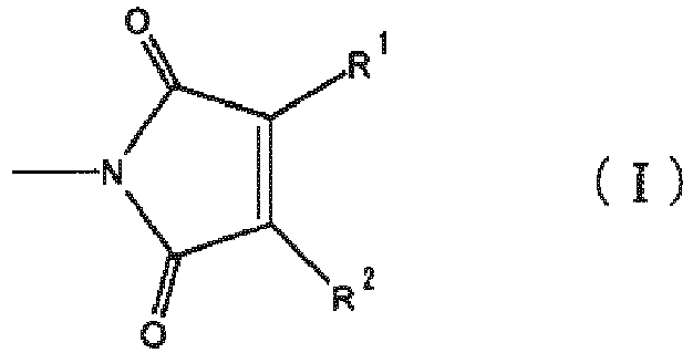
- The maleimide compound is preferably liquid at room temperature and therefore the moiety (I) bonds to a group that allows the maleimide compound to be liquid, for example, an organic group having a branched alkyl, alkylene, alkylene oxide, alkylene carboxyl, or alkylene amide structure having sufficient length and branches to render the maleimide compound liquid. The maleimide compound may have one, or two or more structures (I). The compound having two of these groups is a bismaleimide compound. In addition, a maleimide compound, even if it is not liquid, may be used if the composition becomes liquid as being mixed with another maleimide compound or mixed with another component.
- Examples of a maleimide compound, in which the moiety (I) bonds to an alkyl group or an alkylene group (the groups may have a double bond, or a saturated aliphatic ring), include the following compounds.


- Particularly preferable examples include stearyl maleimide, oleyl maleimide, behenyl maleimide, and a 1,20-bismaleimide derivative of 10,11-dioctyleicosane, as well as a combination thereof. A 1,20-bismaleimide derivative of 10,11-dioctyleicosane is available from Henkel AG & Co. under a product name of X-BMI, which is synthesized from 1,20-diamino-10,11-dioctyl-eicosane and/or a diamine of a cyclic isomer thereof by a method according to
U.S. Patent No. 5973166 (the entire disclosures ofU.S. Patent No. 5973166 are incorporated herein by reference). X-BMI contains one, or two or more of 1,20-bismaleimide-10,11-dioctyl-eicosane [compound denoted by Formula (X-1)], 1-heptylene maleimide-2-octylene maleimide-4-octyl-5-heptylcyclohexane [compound denoted by Formula (X-2)], 1,2-dioctylene maleimide-3-octyl-4-hexylcyclohexane [compound denoted by Formula (X-3)], and the like. Bismaleimide compounds denoted by formulas (X-1) to (X-3) may be also preferably used solely. - Examples of a maleimide compound, in which the moiety (I) is bonded with a group having an alkylene oxide structure, include the following compounds.

- Examples of another usable maleimide compound include a compound (3,4,5,6-tetrahydrophthaloimide ethyl acrylate) denoted by the following formula.

- The above maleimide compounds may be used singly or in a combination of two or more kinds thereof.
- The content of a maleimide compound in accordance with the present invention is preferably from 0 to 50% by weight based on the total weight of a composition, more preferably from 0.1 to 50% by weight, and further preferably from 1 to 20% by weight. If the content of a maleimide compound is within the range, the curing rate becomes superior.
- Meanwhile, when a composition contains a maleimide compound in accordance with the present invention, the (meth)acrylic compound and the maleimide compound in a composition polymerize by a radical reaction by being heated to a predetermined temperature. In this case, only 1 kind of compound may polymerize to form a homopolymer, or two or more kinds of compounds may polymerize to form a copolymer.
- A composition according to the present invention may contain a filler. By blending a filler, a composition for an electronic device having a low coefficient of linear expansion exhibiting superior dimensional stability and improved flame resistance can be obtained. As a filler, either of an insulating inorganic filler or an electrically conductive inorganic filler may be selected depending on the purpose of use. Examples of an insulating inorganic filler include silica, calcium silicate, aluminum hydroxide, magnesium hydroxide, calcium carbonate, magnesium carbonate, magnesium oxide, aluminum nitride, and boron nitride, and particularly silica is preferable. Examples of an electrically conductive inorganic filler include a metal and carbon black.
- Further, a filler subjected to a surface modification according to need may be also used. Examples of commercial products include a lineup of "Mitsubishi carbon black" from Mitsubishi Chemical Corporation, "Asahi" series from Asahi Carbon Co., Ltd., calcium silicate "PCM Lite" series, aluminum hydroxide "ALH" series, and alumina-based "Celasule" from Kawai Lime Ind. Co., Ltd., titanium oxide "STR series", silica "Sciqus Series", zinc oxide "FINEEX series", magnesium oxide "SMO Series", and zirconium oxide "STR Series" from Sakai Chemical Industry Co., Ltd., silica, oxidized alumina "ADMAFINE" series from Admatechs Company Limited, silica "SNOWTEX" series from Nissan Chemical Ind., Ltd., and a metallic oxide containing silica and aluminum oxide "NanoTek" series from C.I. Kasei Co., Ltd.
- When a composition according to the present invention is used for producing, for example, a semiconductor device, the average particle diameter of a filler is preferably smaller than the gap dimension between a semiconductor chip element formation surface and a wiring substrate. If the average particle diameter of a filler is too large, the filler may be trapped between metal connections in producing a semiconductor device, so that good electrical reliability may not be established, or a chip may break.
- Although the blending amount of a filler may be adjustable depending on the purpose of use, it is preferably, for example, from 1 to 99% by weight based on the total weight of an adhesive composition, and more preferably from 10 to 80% by weight. If the content is within the range, a composition having a sufficient effect of filler addition and a viscosity free from any problem in handling can be obtained.
- A composition according to the present invention contains preferably a radical initiator. As a radical initiator to be used according to the present invention, a thermal radical initiator is preferable. As a thermal radical initiator, an organic peroxide is preferable, and one that generates a radical at a convenient temperature is selected.
- Although there is no particular restriction on a radical initiator, examples thereof include diisobutyl peroxide, cumyl peroxyneodecanate, di-n-propyl peroxycarbonate, diisopropyl peroxycarbonate, di-sec-butyl peroxycarbonate, 1,1,3,3-tetramethylbutyl peroxyneodecanate, di(4-t-butylcyclohexyl)peroxydicarbonate, di(2-ethylhexyl)peroxydicarbonate, t-hexyl peroxyneodecanate, t-butyl peroxyneodecanate, t-butyl peroxyneoheptanate, t-hexyl peroxypivalate, t-butyl peroxypivalate, di(3,5,5-trimethylhexanoyl)peroxide, dilauroyl peroxide, 1,1,3,3-tetramethylbutyl peroxy-2-ethyl hexanate, disuccinic acid peroxide, 2,5-dimethyl-2,5-di(2-ethylhexanoylperoxy)hexane, t-hexyl peroxy-2-ethyl hexanate, di(4-methyl benzoyl)peroxide, t-butylperoxy-2-ethyl hexanate, dibenzoyl peroxide, 1,1-di(t-butylperoxy)-2-methylcyclohexane, 1,1-di(t-hexylperoxy)-3,3,5-trimethyl cyclohexane, 1,1-di(t-hexylperoxy)cyclohexane, 1,1-di(t-butylperoxy)cyclohexane, 2,2-di(4,4-di-(t-butylperoxy)cyclohexyl)propane, t-hexylperoxy isopropyl monocarbonate, t-butyl peroxymaleic acid, t-butyl peroxy-3,5,5-trimethyl hexanate, t-butyl peroxylaurate, t-butyl peroxyisopropyl monocarbonate, t-butylperoxy 2-ethylhexyl monocarbonate, t-hexyl peroxybenzoate, 2,5-di-methyl-2,5-di(benzoyl peroxy)hexane, t-butyl peroxyacetate, 2,2-di(t-butylperoxy)butane, t-butyl peroxybenzoate, n-butyl-4,4-di-(t-butylperoxy)valerate, di(2-t-butyl peroxyisopropyl)benzene, dicumyl peroxide, di-t-hexyl peroxide, t-butyl cumyl peroxide, di-t-butyl peroxide, p-menthane hydroperoxide, 2,5-dimethyl-2,5-di(t-butylperoxy)hexane-3, 3,5-diisopropylbenzene hydroperoxide, 1,1,3,3-tetramethyl butyl hydroperoxide, cumene hydroperoxide, t-butyl hydroperoxide, and 2,3-dimethyl-2,3-diphenyl butane. The organic peroxides can be purchased from Akzo Nobel N.V., Gio specialities Chemical, Arkema S.A., NOF Corporation, Kayaku Akzo Corporation, and the like. The same may be used singly, or in a combination of two or more kinds thereof.
- The blending amount of a radical initiator is preferably from 0.01 to 10% by weight based on the total weight of a composition, and more preferably from 0.1 to 5% by weight. If the blending amount of a radical initiator is within the range, there occurs no problem of instability in applying the composition or of prolongation of a curing time.
- In addition to the aforedescribed components, a composition according to the present invention may contain an additive as needed, such as a silane coupling agent, a rubber component, an antioxidant, a light stabilizer, a radical stabilizing agent, and a surfactant. A silane coupling agent and a rubber component can advantageously improve the adhesive property of a composition, relax a stress, and reduce warping of a cured reaction product. Meanwhile, an antioxidant, and a radical stabilizing agent may be used in order to extend the pot life. A surfactant may be added for defoaming in coating, or for improving the wettability to a target to be coated and the leveling property.
- By blending a silane coupling agent to a composition the adhesive property of an adhesive can be improved.
- Although there is no particular restriction on a silane coupling agent, examples thereof include an aminosilane coupling agent, an epoxy silane coupling agent, a ureide silane coupling agent, an isocyanate silane coupling agent, a vinyl silane coupling agent, a (meth)acrylic silane coupling agent, and a ketimine silane coupling agent, and among these, an isocyanate silane coupling agent, a (meth)acrylic silane coupling agent, and an epoxy silane coupling agent are preferable. The silane coupling agents can be purchased from Dow Corning Toray Silicone Co., Ltd., Shin-Etsu Silicone, Matsumoto Fine Chemical Co., Ltd., Tokyo Chemical Industry Co., Ltd. and the like.
- Although the blending amount of a silane coupling agent is adjustable appropriately, it is preferably, for example, from 0 to 10% by weight based on the total weight of a composition, and more preferably from 0 to 5% by weight. If the content of a silane coupling agent is too high, a silane coupling agent vaporizes during thermal compression bonding in a flip chip process to develop voids.
- Although there is no particular restriction on rubber, examples thereof include industrial rubbers, such as acrylic rubber, nitrile rubber, butadiene rubber, and nitrile butadiene rubber, and a low molecular weight crosslinking agent for rubber. Examples of commercial products for industrial rubbers include "Paracron RP" series from Negami Chemical Industrial Co., Ltd., "Staphyloid IM" series and "Staphyloid AC" series from Ganz Chemical Co., Ltd., "Zeon" series from Zeon Kasei Co., Ltd., and "METABLEN C/E/W/S/SX/SRX" from Mitsubishi Rayon Co., Ltd. Examples of commercial products for a low molecular weight crosslinking agent for rubber include "Ricon" series from Sartomer, "Poly bd" and "Poly ip" series, "EPOL" series, and "Krasol" from Idemitsu Kosan Co., Ltd., and "NISSO-PB" from Nippon Soda Co., Ltd. The products may be used singly or in a combination of two or more kinds thereof.
- Further, a commercial product of an acrylic resin, in which a rubber particle has been dispersed in advance, may be used, and examples thereof include Paracron SN-50, AS-3000, ME-2000, W-1163, W-248E, W-197C, PRECOAT 200, and PANLON S-2012 from Negami Chemical Industrial Co., Ltd.
- Although the blending amount of rubber is adjustable appropriately, it is preferably, for example, from 0 to 30% by weight based on the total weight of an adhesive composition, and more preferably from 0 to 20% by weight. If the rubber content is too high, the viscosity of an adhesive composition increases too much causing such problems that the handling property may be deteriorated, or mixing of other components may become difficult, or the adhesiveness of an adhesive may be deteriorated.
- Examples include for an antioxidant and a radical stabilizing agent hydroquinones, benzoquinones, and hindered phenols; and for a light stabilizer benzotriazole-based, triazine-based, benzophenone-based, benzoate-based, and hindered amine-based ultraviolet absorbers. A surfactant may be selected out of catalogs of commercial products depending on a purpose of use.
- A composition according to the present invention can be obtained by mixing uniformly the above specified respective components, as well as a solvent according to need. A composition is only required that a viscosity thereof is adjusted as long as it can be applied by a coater such as a dispenser, and may be also solventless. It is also possible to adjust viscosity by selection of compounds in a composition, or by adjustment of the blending amounts thereof. A composition according to the present invention can be produced by kneading uniformly predetermined amounts of the respective components by, without limitation thereto, using singly or in a combination of publicly known various kneading machines, such as a homodisperser, a universal mixer, a Banbury mixer, a kneader, a twin roll mill, a triple roll mill, and an extruder. Kneading may be conducted under various conditions, such as at normal temperature or with heating, at a normal pressure, a reduced pressure, or an increased pressure, or with inert gas flow.
- A composition for an electronic device according to the present invention is used preferably for an electronic device, particularly as an underfill sealant (sealant) in a device including a semiconductor chip, but without limitation thereto.
- Next, a production method of an electronic device comprising a composition according to the present invention will be described. Although there is no particular restriction on a production method of an electronic device, a flip chip process is preferably used. In a flip chip process, it is particularly preferable to coat a circuit face of a wiring substrate with a composition according to the present invention. A production method of an electronic device comprises, for example,
- (1) a coating process for coating a circuit face of a wiring substrate with a composition according to the present invention, and
- (2) a bonding and sealing process for placing a semiconductor chip on the composition applied on the wiring substrate, and performing electrical connection between the semiconductor chip and the wiring substrate and seal of a gap therebetween. The respective processes will be described below.
- In the coating process, a composition according to the present invention is applied on a circuit face of a wiring substrate. All over the surface of a wiring substrate or only a part where a semiconductor chip is to be mounted may be coated with the composition. Examples of a coating method include coating methods using a spin coater, a dispenser, a roller, and the like and screen printing. In this connection, a syringe used in the coating process, a substrate, and the like may be heated to room temperature or higher as needed so as to improve the flowability of the composition.
- In the bonding and sealing process, electrical connection between the semiconductor element and the wiring substrate is performed, and simultaneously a gap between the semiconductor element and the circuit substrate is sealed with a composition according to the present invention to produce an electronic device. Firstly, a semiconductor chip is placed on a part coated with an adhesive composition on a wiring substrate. On this occasion, a circuit face of the wiring substrate (namely, a face coated with the composition in the coating process) and an element formation surface of the semiconductor chip are so aligned that the two face each other. Then, thermal compression bonding is followed. Heating may be performed additionally after the thermal compression bonding in order to cure the adhesive composition. In general, as a method for thermal compression bonding and connection, thermal compression bonding is performed immediately after position adjustment using a flip chip bonder, or after position adjustment and provisional mounting, heating connection is performed in a reflow oven and the like. On this occasion, a thermal profile suitable for a package or a sealing method is applied. Further, for chip mounting, not only a flip chip bonder, a die bonder and the like, with which position adjustment is possible, may be also used alternatively.
- There is no particular restriction on the temperature for thermal compression bonding. When an electrode is a solder bump or a solder cap bump, a temperature higher than the melting point by 10 to 100°C is preferable, 200°C or higher is preferable, and 210 to 300°C is more preferable. The duration time for thermal compression bonding is preferably from 1 to 20 sec, and the pressure is preferably from 0.1 to 7 MPa. Further, if additional heating is performed for curing completely an adhesive composition after the thermal compression bonding, for example, 150 to 220°C for 30 to 180 min are preferable.
- An electronic device obtained as above can be applied to various electronic appliances utilizing a semiconductor chip, such as a cell phone, a personal computer, and a TV.
- The present invention will be described below in more details by way of Examples. However, the present invention is not restricted by the following Examples.
- Table 1 shows compounds used in the following Examples and Comparative Examples.
[Table 1] Component Name of source material Description of compound (Meth)acrylate CN120 (produced by Sartomer) Epoxy acrylate oligomer SR9003 (produced by Sartomer) Propoxylated neopentyl glycol diacrylate SR480 (produced by Sartomer) Ethoxylated bisphenol A dimethacrylate SR444 (produced by Sartomer) Pentaerythritol triacrylate Maleimide LUMICURE MIA200 produced byDIC Corporation Polyalkylene maleimide acetate Thermal radical initiator Perbutyl Z (produced by NOF Corporation) t-butyl peroxybenzoate Filler SE-2030 (produced by Admatechs Co., Ltd.) Silica Coupling agent KBM-503 (produced by Shin-Etsu Chemical Co., Ltd.) 3-Methacryloxypropyltrimethoxysilane Isocyanuric acid having allyl group TAIC (registered trademark) (produced by Nippon Kasei Chemical Co., Ltd.) Triallyl isocyanurate TAIC (registered trademark) Prepolymer (produced by Nippon Kasei Chemical Co., Ltd.) Powder not volatile during high temperature crosslinking, prepared by prepolymerizing TAIC (registered trademark) TMAIC (registered trademark) (produced by Nippon Kasei Chemical Co., Ltd.) Trimethallyl isocyanurate DA-MGIC (produced by Shikoku Chemicals Corporation) Diallyl monoglycidyl isocyanurate MA-DGIC (produced by Shikoku Chemicals Corporation) 1-Allyl-3,5-diglycidyl isocyanurate Diallyl isocyanurate (produced by Tokyo Chemical Industry Co., Ltd.) Diallyl propyl isocyanurate (produced by Tokyo Chemical Industry Co., Ltd.) - Apparatus and the like used in the following Examples and Comparative Examples are as follows:
- (1) Circuit substrate: WALTS-KIT MB50-0102JY_CR from Walts Co., Ltd. Pads are according to CuOSP specifications.
- (2) Semiconductor chip: WALTS-TEG MB50-0101JY with 544 bumps constituted with a Cu pillar and solder from Walts Co., Ltd.
- The relevant components were mixed by the following method to prepare an adhesive composition. Table 2 shows compounds blended in the respective Examples and Comparative Examples and the blending amounts thereof (% by weight).
[Table 2] Example Comparative Example 1 2 3 4 5 6 7 8 9 1 2 (Meth)acrylic compound CN120 5 5 5 5 5 5 5 5 15 5 6 SR9003 10 10 10 10 10 10 10 10 10 15 11 SR480 10 10 10 10 10 10 10 10 10 15 11 SR444 10 10 10 10 10 10 10 10 10 15 11 Maleimide compound MIA200 10 10 10 10 10 10 10 10 0 0 11 Coupling agent KBM-503 0.3 0.3 0.3 0.3 0.3 0.3 0.3 0.3 0.3 0.3 0.3 Filler SE2030 49.5 49.5 49.5 49.5 49.5 49.5 49.5 49.5 49.5 49.5 49.5 Radical initiator Perbutyl Z 0.2 0.2 0.2 0.2 0.2 0.2 0.2 0.2 0.2 0.2 0.2 Isocyanuric acid having allyl group TAIC 5 0 0 0 0 0 0 0 0 0 0 TAIC Prepolymer 0 5 0 0 0 0 0 0 0 0 0 TMAIC 0 0 5 0 0 0 0 0 0 0 0 DA-MGIC 0 0 0 5 0 0 0 0 0 0 0 MA-DGIC 0 0 0 0 5 0 0 0 0 0 0 MeDAIC 0 0 0 0 0 5 0 0 0 0 0 Diallyl isocyanurate 0 0 0 0 0 0 5 0 0 0 0 Diallyl propyl isocyanurate 0 0 0 0 0 0 0 5 5 0 0 Total 100 100 100 100 100 100 100 100 100 100 100 (The unit of the number is weight %.) - Compounds listed in Table 2 were weighed out according to the designated blending amounts and kneaded uniformly by a triple roll mill. The product was degassed in vacuum to prepare an adhesive composition A.
- After heating a circuit substrate in an oven at 120°C for 1 hour, the composition A was applied on a circuit substrate with an autodispenser to obtain a circuit substrate B coated with the adhesive composition A.
- Immediately after preparation of the circuit substrate B (heat exposure time 0 min), or after being left standing on a hot plate at 80°C for 15 min, 30 min, 45 min, 60 min, or 90 min, the position of a semiconductor chip and the circuit substrate B was adjusted and the two were pressed together using a flip chip bonder equipped with a pulse heat function, followed by thermal compression bonding with pulse heating at 240°C. Thereafter, the composition A was cured in an oven at 150°C for 1 hour to complete an electronic device C.
- The electrical continuity of the above produced electronic device C was examined to find that the electrical continuity was good with respect to any heat exposure time on the hot plate at 80°C (Table 3). Namely, all of the 544 bumps on the semiconductor chip were connected. Therefore, it was demonstrated that the composition in Example 1 maintained liquidity sufficient for processing, even if the same was left standing on a hot plate at 80°C.
[Table 3] Time for being left Electrical continuity 0 minutes good 15 minutes good 30 minutes good 45 minutes good 60 minutes good 90 minutes good - Electronic devices were produced by the same method as in Example 1, except that the components to be blended in the compositions were changed as shown in Table 2. Also in Examples 2 to 9, circuit substrates coated with the compositions were left standing at 80°C for 0 min, 15 min, 30 min, 45 min, 60 min, and 90 min, then electronic devices were produced, and the electrical continuity thereof were examined. As the results, for all the cases, good electrical continuity was obtained. Therefore, it was demonstrated that the compositions in Examples 2 to 9 also maintained liquidity sufficient for processing, even if the same were left standing on a hot plate at 80°C.
- An electronic device was produced by the same method as in Example 1, except that the components to be blended in a composition were changed as shown in Table 2 and a maleimide compound and an isocyanuric acid having an allyl group were not blended. Also in Comparative Example 1, circuit substrates coated with the composition were left standing at 80°C for 0 min, 15 min, 30 min, 45 min, 60 min, and 90 min, then electronic devices were produced, and the electrical continuity thereof were examined. As the results, good electrical continuity of an electronic device produced without being left standing at 80°C (heat exposure time 0 min) was confirmed, however in all other cases, electrical continuity was not established (Table 4). Therefore, it was demonstrated that curing of the composition in Comparative Example 1 had progressed by being left standing at 80°C, and good electrical continuity could not be established.
[Table 4] Time for being left Electrical continuity 0 minutes good 15 minutes unconnected 30 minutes unconnected 45 minutes unconnected 60 minutes unconnected 90 minutes unconnected - An electronic device was produced by the same method as in Example 1, except that the components to be blended in a composition were changed as shown in Table 2 and an isocyanuric acid having an allyl group was not blended. Also in Comparative Example 2, the electrical continuity was examined as in Example 1. As the results, good electrical continuity of an electronic device produced without being left standing at 80°C (heat exposure time 0 min) was confirmed, however in all other cases (left standing at 80°C), electrical continuity was not established. It was confirmed that curing of the composition in Comparative Example 2 had also progressed by being left standing at 80°C, and good electrical continuity could not be established.
Claims (9)
- An underfill sealant composition comprising:(a) a (meth)acrylic compound and(c) an isocyanuric acid having an allyl group.
- The composition according to Claim 1, further comprising (b) a maleimide compound.
- The composition according to Claim 2, wherein the maleimide compound (b) comprises a bismaleimide.
- The composition according to any one of Claims 1 to 3, further comprising a radical initiator.
- The composition according to any one of Claims 1 to 4 comprising:10-90 wt% of the (meth)acrylic compound (a) based on the total weight of the composition and0.001-20 wt% of the isocyanuric acid having an allyl group (c) based on the total weight of the composition.
- The composition according to any one of Claims 2 to 5, comprising 0.1-50 wt% of the maleimide compound (b) based on the total weight of the composition.
- The composition according to any one of Claims 1 to 6, which is used in flip chip mounting.
- An electronic device comprising a cured product of the composition according to any one of Claims 1 to 7.
- An electronic appliance comprising the electronic device according to Claim 8.
Applications Claiming Priority (2)
| Application Number | Priority Date | Filing Date | Title |
|---|---|---|---|
| PCT/JP2011/070652 WO2013035205A1 (en) | 2011-09-09 | 2011-09-09 | Underfill composition |
| PCT/JP2012/072985 WO2013035869A1 (en) | 2011-09-09 | 2012-09-07 | Underfill composition |
Publications (3)
| Publication Number | Publication Date |
|---|---|
| EP2755233A1 true EP2755233A1 (en) | 2014-07-16 |
| EP2755233A4 EP2755233A4 (en) | 2015-06-03 |
| EP2755233B1 EP2755233B1 (en) | 2016-11-02 |
Family
ID=47831687
Family Applications (1)
| Application Number | Title | Priority Date | Filing Date |
|---|---|---|---|
| EP12830373.2A Not-in-force EP2755233B1 (en) | 2011-09-09 | 2012-09-07 | Underfill composition |
Country Status (8)
| Country | Link |
|---|---|
| US (1) | US9334429B2 (en) |
| EP (1) | EP2755233B1 (en) |
| JP (1) | JP6182069B2 (en) |
| KR (1) | KR101926898B1 (en) |
| CN (1) | CN103875065B (en) |
| SG (1) | SG11201400491UA (en) |
| TW (1) | TWI605111B (en) |
| WO (2) | WO2013035205A1 (en) |
Families Citing this family (6)
| Publication number | Priority date | Publication date | Assignee | Title |
|---|---|---|---|---|
| CN105874030B (en) * | 2014-01-02 | 2019-07-26 | 汉高知识产权控股有限责任公司 | Film containing nanoparticle filler |
| CN103980706B (en) * | 2014-05-16 | 2017-01-11 | 广东生益科技股份有限公司 | Thermosetting resin composition and applications thereof |
| CN109312140B (en) * | 2016-05-31 | 2022-03-29 | 三菱瓦斯化学株式会社 | Resin composition, laminate, semiconductor wafer with resin composition layer, substrate for mounting semiconductor with resin composition layer, and semiconductor device |
| JP7154037B2 (en) * | 2017-05-16 | 2022-10-17 | デクセリアルズ株式会社 | UNDERFILL MATERIAL, UNDERFILL FILM, AND METHOD FOR MANUFACTURING SEMICONDUCTOR DEVICE USING THE SAME |
| WO2020035906A1 (en) * | 2018-08-14 | 2020-02-20 | 日立化成株式会社 | Adhesive composition and semiconductor device production method |
| TW202319467A (en) * | 2021-11-03 | 2023-05-16 | 台燿科技股份有限公司 | Resin composition and uses of the same |
Family Cites Families (26)
| Publication number | Priority date | Publication date | Assignee | Title |
|---|---|---|---|---|
| JPS56155214A (en) | 1980-05-02 | 1981-12-01 | Hitachi Ltd | Thermosetting resin composition |
| JPH0762057B2 (en) * | 1990-11-30 | 1995-07-05 | 積水フアインケミカル株式会社 | Curable composition |
| JPH08213517A (en) | 1995-02-03 | 1996-08-20 | Bridgestone Corp | Sealing composition and method of electronic circuit |
| JP3777734B2 (en) | 1996-10-15 | 2006-05-24 | 東レ株式会社 | Adhesive composition for semiconductor device and adhesive sheet for semiconductor device using the same |
| JP3599160B2 (en) | 1997-05-16 | 2004-12-08 | 大日本インキ化学工業株式会社 | Active energy ray-curable composition containing maleimide derivative and method for curing the active energy ray-curable composition |
| US5973166A (en) | 1998-03-02 | 1999-10-26 | The Dexter Corporation | Method for the preparation of maleimides |
| JP2001302736A (en) * | 2000-02-17 | 2001-10-31 | Nof Corp | Polymer insulating material, method for producing the same, electronic-related substrate and electronic member |
| JP3633422B2 (en) | 2000-02-22 | 2005-03-30 | ソニーケミカル株式会社 | Connecting material |
| JP2005330333A (en) * | 2004-05-18 | 2005-12-02 | Du Pont Mitsui Polychem Co Ltd | Polymer composition and production method thereof |
| US20070299181A1 (en) * | 2003-05-23 | 2007-12-27 | Du Pont-Mitsui Polychemicals Co., Ltd. | Polymer composition, process for producing the polymer composition, and molded articles for automobile exterior trim |
| CN1930263B (en) | 2004-03-19 | 2012-02-29 | 住友电木株式会社 | Resin composition and semiconductor device manufactured using the resin composition |
| JP4451214B2 (en) | 2004-05-21 | 2010-04-14 | シャープ株式会社 | Semiconductor device |
| GB0413630D0 (en) | 2004-06-18 | 2004-07-21 | Avecia Ltd | Process |
| JP5140996B2 (en) * | 2006-08-29 | 2013-02-13 | 日立化成工業株式会社 | Adhesive composition, circuit connection material, circuit member connection structure, and semiconductor device |
| JP5560544B2 (en) | 2007-08-29 | 2014-07-30 | 日立化成株式会社 | Adhesive composition, film adhesive, circuit connecting adhesive, connector, and semiconductor device |
| JP5014945B2 (en) | 2007-10-17 | 2012-08-29 | シャープ株式会社 | Semiconductor device |
| JP2009256581A (en) | 2008-03-28 | 2009-11-05 | Hitachi Chem Co Ltd | Adhesive composition, adhesive for circuit connection and connected product using the same |
| JP5251393B2 (en) | 2008-03-28 | 2013-07-31 | 日立化成株式会社 | Adhesive composition, adhesive for circuit connection, and connection body using the same |
| KR20110034038A (en) * | 2008-08-04 | 2011-04-04 | 히다치 가세고교 가부시끼가이샤 | Adhesive Compositions, Film Adhesives, Adhesive Sheets, and Semiconductor Devices |
| KR101097428B1 (en) * | 2008-12-11 | 2011-12-23 | 제일모직주식회사 | Anisotropic conductive film composition and anisotropic conductive film using it |
| JP5251555B2 (en) | 2009-02-02 | 2013-07-31 | 日立化成株式会社 | Photosensitive resin composition, and photosensitive element, solder resist and printed wiring board using the same |
| WO2010098324A1 (en) | 2009-02-27 | 2010-09-02 | ソニーケミカル&インフォメーションデバイス株式会社 | Method of producing semiconductor device |
| WO2010144792A1 (en) * | 2009-06-11 | 2010-12-16 | Rogers Corporation | Dielectric materials, methods of forming subassemblies therefrom, and the subassemblies formed therewith |
| JP5454018B2 (en) | 2009-09-01 | 2014-03-26 | 日立化成株式会社 | Film adhesive, adhesive sheet and semiconductor device |
| KR101023241B1 (en) | 2009-12-28 | 2011-03-21 | 제일모직주식회사 | Adhesive composition for semiconductor and adhesive film using same |
| KR101924049B1 (en) * | 2011-11-02 | 2018-12-03 | 헨켈 아이피 앤드 홀딩 게엠베하 | Adhesive for electronic component |
-
2011
- 2011-09-09 WO PCT/JP2011/070652 patent/WO2013035205A1/en not_active Ceased
-
2012
- 2012-08-29 TW TW101131291A patent/TWI605111B/en not_active IP Right Cessation
- 2012-09-07 CN CN201280049573.2A patent/CN103875065B/en not_active Expired - Fee Related
- 2012-09-07 EP EP12830373.2A patent/EP2755233B1/en not_active Not-in-force
- 2012-09-07 SG SG11201400491UA patent/SG11201400491UA/en unknown
- 2012-09-07 JP JP2013532686A patent/JP6182069B2/en not_active Expired - Fee Related
- 2012-09-07 WO PCT/JP2012/072985 patent/WO2013035869A1/en not_active Ceased
- 2012-09-07 KR KR1020147005978A patent/KR101926898B1/en not_active Expired - Fee Related
-
2014
- 2014-03-07 US US14/200,871 patent/US9334429B2/en not_active Expired - Fee Related
Also Published As
| Publication number | Publication date |
|---|---|
| KR20140068929A (en) | 2014-06-09 |
| US9334429B2 (en) | 2016-05-10 |
| KR101926898B1 (en) | 2018-12-07 |
| JPWO2013035869A1 (en) | 2015-03-23 |
| EP2755233B1 (en) | 2016-11-02 |
| CN103875065B (en) | 2017-02-15 |
| US20140187729A1 (en) | 2014-07-03 |
| WO2013035869A1 (en) | 2013-03-14 |
| JP6182069B2 (en) | 2017-08-16 |
| EP2755233A4 (en) | 2015-06-03 |
| CN103875065A (en) | 2014-06-18 |
| SG11201400491UA (en) | 2014-08-28 |
| WO2013035205A1 (en) | 2013-03-14 |
| TWI605111B (en) | 2017-11-11 |
| TW201321487A (en) | 2013-06-01 |
Similar Documents
| Publication | Publication Date | Title |
|---|---|---|
| US9771500B2 (en) | Sealant composition for electronic device | |
| EP2755234B1 (en) | Composition for electronic device | |
| US9334429B2 (en) | Underfill sealant composition | |
| CN104039913B (en) | Adhesive for electronic unit |
Legal Events
| Date | Code | Title | Description |
|---|---|---|---|
| PUAI | Public reference made under article 153(3) epc to a published international application that has entered the european phase |
Free format text: ORIGINAL CODE: 0009012 |
|
| 17P | Request for examination filed |
Effective date: 20140321 |
|
| AK | Designated contracting states |
Kind code of ref document: A1 Designated state(s): AL AT BE BG CH CY CZ DE DK EE ES FI FR GB GR HR HU IE IS IT LI LT LU LV MC MK MT NL NO PL PT RO RS SE SI SK SM TR |
|
| DAX | Request for extension of the european patent (deleted) | ||
| RA4 | Supplementary search report drawn up and despatched (corrected) |
Effective date: 20150507 |
|
| RIC1 | Information provided on ipc code assigned before grant |
Ipc: C09D 135/00 20060101ALI20150429BHEP Ipc: C08F 220/26 20060101ALI20150429BHEP Ipc: H01L 21/60 20060101AFI20150429BHEP Ipc: H01L 23/29 20060101ALI20150429BHEP Ipc: H01L 23/31 20060101ALI20150429BHEP Ipc: C08F 226/06 20060101ALI20150429BHEP Ipc: C08F 222/40 20060101ALI20150429BHEP Ipc: C08F 220/10 20060101ALI20150429BHEP Ipc: C09D 4/06 20060101ALI20150429BHEP |
|
| GRAP | Despatch of communication of intention to grant a patent |
Free format text: ORIGINAL CODE: EPIDOSNIGR1 |
|
| INTG | Intention to grant announced |
Effective date: 20160530 |
|
| GRAS | Grant fee paid |
Free format text: ORIGINAL CODE: EPIDOSNIGR3 |
|
| GRAA | (expected) grant |
Free format text: ORIGINAL CODE: 0009210 |
|
| AK | Designated contracting states |
Kind code of ref document: B1 Designated state(s): AL AT BE BG CH CY CZ DE DK EE ES FI FR GB GR HR HU IE IS IT LI LT LU LV MC MK MT NL NO PL PT RO RS SE SI SK SM TR |
|
| REG | Reference to a national code |
Ref country code: GB Ref legal event code: FG4D |
|
| REG | Reference to a national code |
Ref country code: AT Ref legal event code: REF Ref document number: 842607 Country of ref document: AT Kind code of ref document: T Effective date: 20161115 Ref country code: CH Ref legal event code: EP |
|
| REG | Reference to a national code |
Ref country code: IE Ref legal event code: FG4D |
|
| REG | Reference to a national code |
Ref country code: DE Ref legal event code: R096 Ref document number: 602012024989 Country of ref document: DE |
|
| REG | Reference to a national code |
Ref country code: NL Ref legal event code: FP |
|
| PG25 | Lapsed in a contracting state [announced via postgrant information from national office to epo] |
Ref country code: LV Free format text: LAPSE BECAUSE OF FAILURE TO SUBMIT A TRANSLATION OF THE DESCRIPTION OR TO PAY THE FEE WITHIN THE PRESCRIBED TIME-LIMIT Effective date: 20161102 |
|
| REG | Reference to a national code |
Ref country code: LT Ref legal event code: MG4D |
|
| REG | Reference to a national code |
Ref country code: AT Ref legal event code: MK05 Ref document number: 842607 Country of ref document: AT Kind code of ref document: T Effective date: 20161102 |
|
| PG25 | Lapsed in a contracting state [announced via postgrant information from national office to epo] |
Ref country code: GR Free format text: LAPSE BECAUSE OF FAILURE TO SUBMIT A TRANSLATION OF THE DESCRIPTION OR TO PAY THE FEE WITHIN THE PRESCRIBED TIME-LIMIT Effective date: 20170203 Ref country code: NO Free format text: LAPSE BECAUSE OF FAILURE TO SUBMIT A TRANSLATION OF THE DESCRIPTION OR TO PAY THE FEE WITHIN THE PRESCRIBED TIME-LIMIT Effective date: 20170202 Ref country code: SE Free format text: LAPSE BECAUSE OF FAILURE TO SUBMIT A TRANSLATION OF THE DESCRIPTION OR TO PAY THE FEE WITHIN THE PRESCRIBED TIME-LIMIT Effective date: 20161102 Ref country code: LT Free format text: LAPSE BECAUSE OF FAILURE TO SUBMIT A TRANSLATION OF THE DESCRIPTION OR TO PAY THE FEE WITHIN THE PRESCRIBED TIME-LIMIT Effective date: 20161102 |
|
| PG25 | Lapsed in a contracting state [announced via postgrant information from national office to epo] |
Ref country code: FI Free format text: LAPSE BECAUSE OF FAILURE TO SUBMIT A TRANSLATION OF THE DESCRIPTION OR TO PAY THE FEE WITHIN THE PRESCRIBED TIME-LIMIT Effective date: 20161102 Ref country code: AT Free format text: LAPSE BECAUSE OF FAILURE TO SUBMIT A TRANSLATION OF THE DESCRIPTION OR TO PAY THE FEE WITHIN THE PRESCRIBED TIME-LIMIT Effective date: 20161102 Ref country code: RS Free format text: LAPSE BECAUSE OF FAILURE TO SUBMIT A TRANSLATION OF THE DESCRIPTION OR TO PAY THE FEE WITHIN THE PRESCRIBED TIME-LIMIT Effective date: 20161102 Ref country code: PL Free format text: LAPSE BECAUSE OF FAILURE TO SUBMIT A TRANSLATION OF THE DESCRIPTION OR TO PAY THE FEE WITHIN THE PRESCRIBED TIME-LIMIT Effective date: 20161102 Ref country code: HR Free format text: LAPSE BECAUSE OF FAILURE TO SUBMIT A TRANSLATION OF THE DESCRIPTION OR TO PAY THE FEE WITHIN THE PRESCRIBED TIME-LIMIT Effective date: 20161102 Ref country code: PT Free format text: LAPSE BECAUSE OF FAILURE TO SUBMIT A TRANSLATION OF THE DESCRIPTION OR TO PAY THE FEE WITHIN THE PRESCRIBED TIME-LIMIT Effective date: 20170302 Ref country code: ES Free format text: LAPSE BECAUSE OF FAILURE TO SUBMIT A TRANSLATION OF THE DESCRIPTION OR TO PAY THE FEE WITHIN THE PRESCRIBED TIME-LIMIT Effective date: 20161102 Ref country code: IS Free format text: LAPSE BECAUSE OF FAILURE TO SUBMIT A TRANSLATION OF THE DESCRIPTION OR TO PAY THE FEE WITHIN THE PRESCRIBED TIME-LIMIT Effective date: 20170302 |
|
| PG25 | Lapsed in a contracting state [announced via postgrant information from national office to epo] |
Ref country code: RO Free format text: LAPSE BECAUSE OF FAILURE TO SUBMIT A TRANSLATION OF THE DESCRIPTION OR TO PAY THE FEE WITHIN THE PRESCRIBED TIME-LIMIT Effective date: 20161102 Ref country code: EE Free format text: LAPSE BECAUSE OF FAILURE TO SUBMIT A TRANSLATION OF THE DESCRIPTION OR TO PAY THE FEE WITHIN THE PRESCRIBED TIME-LIMIT Effective date: 20161102 Ref country code: SK Free format text: LAPSE BECAUSE OF FAILURE TO SUBMIT A TRANSLATION OF THE DESCRIPTION OR TO PAY THE FEE WITHIN THE PRESCRIBED TIME-LIMIT Effective date: 20161102 Ref country code: DK Free format text: LAPSE BECAUSE OF FAILURE TO SUBMIT A TRANSLATION OF THE DESCRIPTION OR TO PAY THE FEE WITHIN THE PRESCRIBED TIME-LIMIT Effective date: 20161102 Ref country code: CZ Free format text: LAPSE BECAUSE OF FAILURE TO SUBMIT A TRANSLATION OF THE DESCRIPTION OR TO PAY THE FEE WITHIN THE PRESCRIBED TIME-LIMIT Effective date: 20161102 |
|
| REG | Reference to a national code |
Ref country code: DE Ref legal event code: R097 Ref document number: 602012024989 Country of ref document: DE |
|
| PG25 | Lapsed in a contracting state [announced via postgrant information from national office to epo] |
Ref country code: SM Free format text: LAPSE BECAUSE OF FAILURE TO SUBMIT A TRANSLATION OF THE DESCRIPTION OR TO PAY THE FEE WITHIN THE PRESCRIBED TIME-LIMIT Effective date: 20161102 Ref country code: BE Free format text: LAPSE BECAUSE OF FAILURE TO SUBMIT A TRANSLATION OF THE DESCRIPTION OR TO PAY THE FEE WITHIN THE PRESCRIBED TIME-LIMIT Effective date: 20161102 Ref country code: IT Free format text: LAPSE BECAUSE OF FAILURE TO SUBMIT A TRANSLATION OF THE DESCRIPTION OR TO PAY THE FEE WITHIN THE PRESCRIBED TIME-LIMIT Effective date: 20161102 Ref country code: BG Free format text: LAPSE BECAUSE OF FAILURE TO SUBMIT A TRANSLATION OF THE DESCRIPTION OR TO PAY THE FEE WITHIN THE PRESCRIBED TIME-LIMIT Effective date: 20170202 |
|
| PLBE | No opposition filed within time limit |
Free format text: ORIGINAL CODE: 0009261 |
|
| STAA | Information on the status of an ep patent application or granted ep patent |
Free format text: STATUS: NO OPPOSITION FILED WITHIN TIME LIMIT |
|
| REG | Reference to a national code |
Ref country code: FR Ref legal event code: PLFP Year of fee payment: 6 |
|
| 26N | No opposition filed |
Effective date: 20170803 |
|
| PG25 | Lapsed in a contracting state [announced via postgrant information from national office to epo] |
Ref country code: SI Free format text: LAPSE BECAUSE OF FAILURE TO SUBMIT A TRANSLATION OF THE DESCRIPTION OR TO PAY THE FEE WITHIN THE PRESCRIBED TIME-LIMIT Effective date: 20161102 |
|
| REG | Reference to a national code |
Ref country code: CH Ref legal event code: PL |
|
| GBPC | Gb: european patent ceased through non-payment of renewal fee |
Effective date: 20170907 |
|
| PG25 | Lapsed in a contracting state [announced via postgrant information from national office to epo] |
Ref country code: MC Free format text: LAPSE BECAUSE OF FAILURE TO SUBMIT A TRANSLATION OF THE DESCRIPTION OR TO PAY THE FEE WITHIN THE PRESCRIBED TIME-LIMIT Effective date: 20161102 |
|
| REG | Reference to a national code |
Ref country code: IE Ref legal event code: MM4A |
|
| PG25 | Lapsed in a contracting state [announced via postgrant information from national office to epo] |
Ref country code: LU Free format text: LAPSE BECAUSE OF NON-PAYMENT OF DUE FEES Effective date: 20170907 |
|
| PG25 | Lapsed in a contracting state [announced via postgrant information from national office to epo] |
Ref country code: IE Free format text: LAPSE BECAUSE OF NON-PAYMENT OF DUE FEES Effective date: 20170907 Ref country code: GB Free format text: LAPSE BECAUSE OF NON-PAYMENT OF DUE FEES Effective date: 20170907 Ref country code: LI Free format text: LAPSE BECAUSE OF NON-PAYMENT OF DUE FEES Effective date: 20170930 Ref country code: CH Free format text: LAPSE BECAUSE OF NON-PAYMENT OF DUE FEES Effective date: 20170930 |
|
| REG | Reference to a national code |
Ref country code: FR Ref legal event code: PLFP Year of fee payment: 7 |
|
| PG25 | Lapsed in a contracting state [announced via postgrant information from national office to epo] |
Ref country code: MT Free format text: LAPSE BECAUSE OF NON-PAYMENT OF DUE FEES Effective date: 20170907 |
|
| PGFP | Annual fee paid to national office [announced via postgrant information from national office to epo] |
Ref country code: FR Payment date: 20180925 Year of fee payment: 7 Ref country code: DE Payment date: 20180920 Year of fee payment: 7 |
|
| PGFP | Annual fee paid to national office [announced via postgrant information from national office to epo] |
Ref country code: NL Payment date: 20180919 Year of fee payment: 7 |
|
| PG25 | Lapsed in a contracting state [announced via postgrant information from national office to epo] |
Ref country code: HU Free format text: LAPSE BECAUSE OF FAILURE TO SUBMIT A TRANSLATION OF THE DESCRIPTION OR TO PAY THE FEE WITHIN THE PRESCRIBED TIME-LIMIT; INVALID AB INITIO Effective date: 20120907 |
|
| PG25 | Lapsed in a contracting state [announced via postgrant information from national office to epo] |
Ref country code: CY Free format text: LAPSE BECAUSE OF NON-PAYMENT OF DUE FEES Effective date: 20161102 |
|
| PG25 | Lapsed in a contracting state [announced via postgrant information from national office to epo] |
Ref country code: MK Free format text: LAPSE BECAUSE OF FAILURE TO SUBMIT A TRANSLATION OF THE DESCRIPTION OR TO PAY THE FEE WITHIN THE PRESCRIBED TIME-LIMIT Effective date: 20161102 |
|
| PG25 | Lapsed in a contracting state [announced via postgrant information from national office to epo] |
Ref country code: TR Free format text: LAPSE BECAUSE OF FAILURE TO SUBMIT A TRANSLATION OF THE DESCRIPTION OR TO PAY THE FEE WITHIN THE PRESCRIBED TIME-LIMIT Effective date: 20161102 |
|
| REG | Reference to a national code |
Ref country code: DE Ref legal event code: R119 Ref document number: 602012024989 Country of ref document: DE |
|
| REG | Reference to a national code |
Ref country code: NL Ref legal event code: MM Effective date: 20191001 |
|
| PG25 | Lapsed in a contracting state [announced via postgrant information from national office to epo] |
Ref country code: AL Free format text: LAPSE BECAUSE OF FAILURE TO SUBMIT A TRANSLATION OF THE DESCRIPTION OR TO PAY THE FEE WITHIN THE PRESCRIBED TIME-LIMIT Effective date: 20161102 Ref country code: NL Free format text: LAPSE BECAUSE OF NON-PAYMENT OF DUE FEES Effective date: 20191001 Ref country code: DE Free format text: LAPSE BECAUSE OF NON-PAYMENT OF DUE FEES Effective date: 20200401 |
|
| PG25 | Lapsed in a contracting state [announced via postgrant information from national office to epo] |
Ref country code: FR Free format text: LAPSE BECAUSE OF NON-PAYMENT OF DUE FEES Effective date: 20190930 |