EP2752880A2 - Graphene electronic devices and methods of manufacturing the same - Google Patents
Graphene electronic devices and methods of manufacturing the same Download PDFInfo
- Publication number
- EP2752880A2 EP2752880A2 EP14150063.7A EP14150063A EP2752880A2 EP 2752880 A2 EP2752880 A2 EP 2752880A2 EP 14150063 A EP14150063 A EP 14150063A EP 2752880 A2 EP2752880 A2 EP 2752880A2
- Authority
- EP
- European Patent Office
- Prior art keywords
- layer
- graphene
- gate
- gate structure
- region
- Prior art date
- Legal status (The legal status is an assumption and is not a legal conclusion. Google has not performed a legal analysis and makes no representation as to the accuracy of the status listed.)
- Granted
Links
Images




Classifications
-
- H—ELECTRICITY
- H10—SEMICONDUCTOR DEVICES; ELECTRIC SOLID-STATE DEVICES NOT OTHERWISE PROVIDED FOR
- H10D—INORGANIC ELECTRIC SEMICONDUCTOR DEVICES
- H10D30/00—Field-effect transistors [FET]
- H10D30/01—Manufacture or treatment
-
- H—ELECTRICITY
- H10—SEMICONDUCTOR DEVICES; ELECTRIC SOLID-STATE DEVICES NOT OTHERWISE PROVIDED FOR
- H10D—INORGANIC ELECTRIC SEMICONDUCTOR DEVICES
- H10D30/00—Field-effect transistors [FET]
- H10D30/01—Manufacture or treatment
- H10D30/021—Manufacture or treatment of FETs having insulated gates [IGFET]
-
- B—PERFORMING OPERATIONS; TRANSPORTING
- B82—NANOTECHNOLOGY
- B82Y—SPECIFIC USES OR APPLICATIONS OF NANOSTRUCTURES; MEASUREMENT OR ANALYSIS OF NANOSTRUCTURES; MANUFACTURE OR TREATMENT OF NANOSTRUCTURES
- B82Y10/00—Nanotechnology for information processing, storage or transmission, e.g. quantum computing or single electron logic
-
- H—ELECTRICITY
- H10—SEMICONDUCTOR DEVICES; ELECTRIC SOLID-STATE DEVICES NOT OTHERWISE PROVIDED FOR
- H10B—ELECTRONIC MEMORY DEVICES
- H10B41/00—Electrically erasable-and-programmable ROM [EEPROM] devices comprising floating gates
- H10B41/30—Electrically erasable-and-programmable ROM [EEPROM] devices comprising floating gates characterised by the memory core region
-
- H—ELECTRICITY
- H10—SEMICONDUCTOR DEVICES; ELECTRIC SOLID-STATE DEVICES NOT OTHERWISE PROVIDED FOR
- H10B—ELECTRONIC MEMORY DEVICES
- H10B51/00—Ferroelectric RAM [FeRAM] devices comprising ferroelectric memory transistors
- H10B51/30—Ferroelectric RAM [FeRAM] devices comprising ferroelectric memory transistors characterised by the memory core region
-
- H—ELECTRICITY
- H10—SEMICONDUCTOR DEVICES; ELECTRIC SOLID-STATE DEVICES NOT OTHERWISE PROVIDED FOR
- H10D—INORGANIC ELECTRIC SEMICONDUCTOR DEVICES
- H10D30/00—Field-effect transistors [FET]
- H10D30/40—FETs having zero-dimensional [0D], one-dimensional [1D] or two-dimensional [2D] charge carrier gas channels
- H10D30/47—FETs having zero-dimensional [0D], one-dimensional [1D] or two-dimensional [2D] charge carrier gas channels having two-dimensional [2D] charge carrier gas channels, e.g. nanoribbon FETs or high electron mobility transistors [HEMT]
-
- H—ELECTRICITY
- H10—SEMICONDUCTOR DEVICES; ELECTRIC SOLID-STATE DEVICES NOT OTHERWISE PROVIDED FOR
- H10D—INORGANIC ELECTRIC SEMICONDUCTOR DEVICES
- H10D30/00—Field-effect transistors [FET]
- H10D30/60—Insulated-gate field-effect transistors [IGFET]
- H10D30/68—Floating-gate IGFETs
- H10D30/681—Floating-gate IGFETs having only two programming levels
-
- H—ELECTRICITY
- H10—SEMICONDUCTOR DEVICES; ELECTRIC SOLID-STATE DEVICES NOT OTHERWISE PROVIDED FOR
- H10D—INORGANIC ELECTRIC SEMICONDUCTOR DEVICES
- H10D30/00—Field-effect transistors [FET]
- H10D30/60—Insulated-gate field-effect transistors [IGFET]
- H10D30/68—Floating-gate IGFETs
- H10D30/6891—Floating-gate IGFETs characterised by the shapes, relative sizes or dispositions of the floating gate electrode
- H10D30/6892—Floating-gate IGFETs characterised by the shapes, relative sizes or dispositions of the floating gate electrode having at least one additional gate other than the floating gate and the control gate, e.g. program gate, erase gate or select gate
-
- H—ELECTRICITY
- H10—SEMICONDUCTOR DEVICES; ELECTRIC SOLID-STATE DEVICES NOT OTHERWISE PROVIDED FOR
- H10D—INORGANIC ELECTRIC SEMICONDUCTOR DEVICES
- H10D30/00—Field-effect transistors [FET]
- H10D30/60—Insulated-gate field-effect transistors [IGFET]
- H10D30/701—IGFETs having ferroelectric gate insulators, e.g. ferroelectric FETs
-
- H—ELECTRICITY
- H10—SEMICONDUCTOR DEVICES; ELECTRIC SOLID-STATE DEVICES NOT OTHERWISE PROVIDED FOR
- H10D—INORGANIC ELECTRIC SEMICONDUCTOR DEVICES
- H10D62/00—Semiconductor bodies, or regions thereof, of devices having potential barriers
- H10D62/80—Semiconductor bodies, or regions thereof, of devices having potential barriers characterised by the materials
- H10D62/83—Semiconductor bodies, or regions thereof, of devices having potential barriers characterised by the materials being Group IV materials, e.g. B-doped Si or undoped Ge
- H10D62/8303—Diamond
-
- H—ELECTRICITY
- H10—SEMICONDUCTOR DEVICES; ELECTRIC SOLID-STATE DEVICES NOT OTHERWISE PROVIDED FOR
- H10D—INORGANIC ELECTRIC SEMICONDUCTOR DEVICES
- H10D62/00—Semiconductor bodies, or regions thereof, of devices having potential barriers
- H10D62/80—Semiconductor bodies, or regions thereof, of devices having potential barriers characterised by the materials
- H10D62/881—Semiconductor bodies, or regions thereof, of devices having potential barriers characterised by the materials being a two-dimensional material
- H10D62/882—Graphene
-
- H—ELECTRICITY
- H10—SEMICONDUCTOR DEVICES; ELECTRIC SOLID-STATE DEVICES NOT OTHERWISE PROVIDED FOR
- H10D—INORGANIC ELECTRIC SEMICONDUCTOR DEVICES
- H10D64/00—Electrodes of devices having potential barriers
- H10D64/01—Manufacture or treatment
- H10D64/031—Manufacture or treatment of data-storage electrodes
- H10D64/033—Manufacture or treatment of data-storage electrodes comprising ferroelectric layers
-
- H—ELECTRICITY
- H10—SEMICONDUCTOR DEVICES; ELECTRIC SOLID-STATE DEVICES NOT OTHERWISE PROVIDED FOR
- H10D—INORGANIC ELECTRIC SEMICONDUCTOR DEVICES
- H10D64/00—Electrodes of devices having potential barriers
- H10D64/01—Manufacture or treatment
- H10D64/031—Manufacture or treatment of data-storage electrodes
- H10D64/035—Manufacture or treatment of data-storage electrodes comprising conductor-insulator-conductor-insulator-semiconductor structures
-
- H—ELECTRICITY
- H10—SEMICONDUCTOR DEVICES; ELECTRIC SOLID-STATE DEVICES NOT OTHERWISE PROVIDED FOR
- H10P—GENERIC PROCESSES OR APPARATUS FOR THE MANUFACTURE OR TREATMENT OF DEVICES COVERED BY CLASS H10
- H10P72/00—Handling or holding of wafers, substrates or devices during manufacture or treatment thereof
- H10P72/70—Handling or holding of wafers, substrates or devices during manufacture or treatment thereof for supporting or gripping
- H10P72/74—Handling or holding of wafers, substrates or devices during manufacture or treatment thereof for supporting or gripping using temporarily an auxiliary support
-
- H—ELECTRICITY
- H10—SEMICONDUCTOR DEVICES; ELECTRIC SOLID-STATE DEVICES NOT OTHERWISE PROVIDED FOR
- H10D—INORGANIC ELECTRIC SEMICONDUCTOR DEVICES
- H10D64/00—Electrodes of devices having potential barriers
- H10D64/20—Electrodes characterised by their shapes, relative sizes or dispositions
- H10D64/23—Electrodes carrying the current to be rectified, amplified, oscillated or switched, e.g. sources, drains, anodes or cathodes
- H10D64/251—Source or drain electrodes for field-effect devices
- H10D64/258—Source or drain electrodes for field-effect devices characterised by the relative positions of the source or drain electrodes with respect to the gate electrode
-
- H—ELECTRICITY
- H10—SEMICONDUCTOR DEVICES; ELECTRIC SOLID-STATE DEVICES NOT OTHERWISE PROVIDED FOR
- H10P—GENERIC PROCESSES OR APPARATUS FOR THE MANUFACTURE OR TREATMENT OF DEVICES COVERED BY CLASS H10
- H10P72/00—Handling or holding of wafers, substrates or devices during manufacture or treatment thereof
- H10P72/70—Handling or holding of wafers, substrates or devices during manufacture or treatment thereof for supporting or gripping
- H10P72/74—Handling or holding of wafers, substrates or devices during manufacture or treatment thereof for supporting or gripping using temporarily an auxiliary support
- H10P72/743—Handling or holding of wafers, substrates or devices during manufacture or treatment thereof for supporting or gripping using temporarily an auxiliary support used as a support during manufacture of interconnect decals or build up layers
-
- H—ELECTRICITY
- H10—SEMICONDUCTOR DEVICES; ELECTRIC SOLID-STATE DEVICES NOT OTHERWISE PROVIDED FOR
- H10P—GENERIC PROCESSES OR APPARATUS FOR THE MANUFACTURE OR TREATMENT OF DEVICES COVERED BY CLASS H10
- H10P72/00—Handling or holding of wafers, substrates or devices during manufacture or treatment thereof
- H10P72/70—Handling or holding of wafers, substrates or devices during manufacture or treatment thereof for supporting or gripping
- H10P72/74—Handling or holding of wafers, substrates or devices during manufacture or treatment thereof for supporting or gripping using temporarily an auxiliary support
- H10P72/744—Details of chemical or physical process used for separating the auxiliary support from a device or a wafer
Definitions
- Example embodiments relate to graphene electronic devices and methods of manufacturing the same.
- Graphene a graphite monoatomic layer
- Graphene is being considered as a next generation material due to its superior electrical and mechanical properties.
- Graphene is a material in which carbon atoms are connected as a hexagon in a plane, and has a relatively small thickness corresponding to a monoatomic layer.
- graphene conducts electricity about a hundred times faster than polycrystalline silicon that is mainly used as a semiconductor, and theoretically has an electron mobility of about 200,000 cm 2 /Vs, 20 m 2 /Vs.
- graphene may conduct electricity about a hundred times more than copper, and thus, graphene is considered as a basic material of electronic devices.
- graphene is a zero gap semiconductor material, and thus, if a graphene nanoribbon (GNR) is manufactured to have a channel width of about 10 nm or less, a band gap is generated due to a size effect.
- GNR graphene nanoribbon
- FET field effect transistor
- graphene is grown on a metal thin film formed of copper (Cu) or nickel (Ni) by a chemical vapor deposition (CVD) method, and then, may be transferred onto an insulating thin film.
- Cu copper
- Ni nickel
- CVD chemical vapor deposition
- Example embodiments provide graphene switching devices including graphene field effect transistors (FETs) and graphene diodes.
- FETs graphene field effect transistors
- Example embodiments provide graphene memory devices formed by combining graphene FETs and graphene diodes.
- At least one example embodiment provides a graphene electronic device.
- the graphene electronic device includes: a first conductive layer and a semiconductor layer on a first region of an intermediate layer; a second conductive layer on a second region of the intermediate layer; a graphene layer on the intermediate layer, the semiconductor layer, and the second conductive layer; and a first gate structure and a second gate structure on the graphene layer.
- the first gate structure may be formed on the graphene layer to correspond to the first region of the intermediate layer.
- the second gate structure may by formed on the graphene layer in a space between the first region and the second region of the intermediate layer.
- the intermediate layer may be formed on a support structure.
- the first gate structure may include a gate insulating layer and a first gate.
- the second gate structure may include the gate insulating layer and a second gate.
- the first gate structure may include a first ferroelectric layer and a first gate.
- the second gate structure may include a second ferroelectric layer and a second gate.
- the first gate structure may include a first tunneling oxide layer, a first floating gate, a first blocking oxide layer, and a first gate.
- the second gate structure may include a second tunneling oxide layer, a second floating gate, a second blocking oxide layer, and a second gate.
- At least one other example embodiment provides a method of forming a graphene electronic device.
- the method includes: forming a semiconductor layer, a first conductive layer, and a second conductive layer on a substrate; forming an intermediate layer on the substrate, the semiconductor layer, the first conductive layer, and the second conductive layer; removing the substrate, and forming a graphene layer on the intermediate layer, the semiconductor layer, and the second conductive layer; and forming a first gate structure and a second gate structure on the graphene layer.
- the method of forming a graphene electronic device may further include: forming a support structure on the intermediate layer, after forming the intermediate layer.
- the substrate may include silicon and a silicon oxide layer, and the substrate may be removed by etching the silicon oxide layer.
- the substrate may include a transparent substrate, and the substrate may be removed by a laser lift-off process.
- the graphene layer may be formed on a catalyst layer by a pyrolisis method or a chemical vapor deposition (CVD) method, after forming the catalyst layer on the intermediate layer.
- CVD chemical vapor deposition
- the graphene electronic device includes: a graphene transistor having a channel including a graphene layer and an electrode including a semiconductor layer; and a graphene tunable diode having a diode region including the graphene layer and the semiconductor layer.
- the graphene transistor may include: a first conductive layer and the semiconductor layer on a first region of an intermediate layer; a second conductive layer on a second region of the intermediate layer; the graphene layer on the intermediate layer, the semiconductor layer, and the second conductive layer; and a gate structure on the graphene layer.
- the graphene tunable diode may include: the semiconductor layer on a first region of an intermediate layer; the graphene layer on the intermediate layer and the semiconductor layer; and a gate structure on the graphene layer corresponding to the first region of the intermediate layer.
- the device may further include: a first conductive layer and the semiconductor layer on a first region of an intermediate layer; a second conductive layer on a second region of the intermediate layer; the graphene layer on the intermediate layer, the semiconductor layer, and the second conductive layer; and a first gate structure and a second gate structure on the graphene layer.
- the device may further include a first gate structure corresponding to the graphene transistor; and a second gate structure corresponding to the graphene tunable diode.
- the gate structure may include a tunneling oxide layer, a floating gate, a blocking oxide layer, and a gate, or the gate structure may include a ferroelectric layer and a gate.
- FIG. 1A is a cross-sectional view of a graphene electronic device 100 according to an example embodiment.
- FIG. 1B is a schematic plan view of the graphene electronic device 100 shown in FIG. 1A.
- FIG. 1A is a cross-sectional view taken along line m1-m2 of FIG. 1B .
- the graphene electronic device 100 includes an intermediate layer 11 formed on a support structure 10, a first conductive layer 12 and a semiconductor layer 13 formed on a first region of the intermediate layer 11, and a second conductive layer 14 formed on a second region of the intermediate layer 11.
- a graphene layer 15 is formed on the intermediate layer 11, the semiconductor layer 13, and the second conductive layer 14.
- First and second gate structures are formed on the graphene layer 15.
- the first gate structure includes a gate insulating layer 16 and a first gate 17.
- the second gate structure includes the gate insulating layer 16 and a second gate 18.
- the first gate structure is formed corresponding to the first region of the intermediate layer 11, and the second gate structure is formed in a space between the first and second regions of the intermediate layer 11.
- the graphene electronic device may be configured to perform functions of a graphene transistor and/or a graphene diode.
- the semiconductor layer 13 and the graphene layer 15 may be a diode region functioning as a graphene tunable diode according to a voltage applied via the first gate 17.
- the first conductive layer 12 and the semiconductor layer 13 in FIG. 1A may be a source electrode
- the second conductive layer 14 may be a drain electrode
- the graphene layer 15 may be a channel region
- the second gate 18 may be a gate electrode.
- the support structure 10 supports each of the layers of the graphene electronic device formed thereon, and may be formed in manufacturing processes for processing stability.
- the support structure 10 may be formed of various materials, for example, a semiconductor substrate such as a Si substrate that is used as a substrate of a semiconductor device, a polymer substrate, an adhesive tape, etc.
- the support structure 10 may include a material having relatively high attachability to the intermediate layer 11, and if necessary, the support structure 10 may be formed of the same or substantially the same material as that of the intermediate layer 11.
- the intermediate layer 11 may be formed of a polymer material, or a material having an insulating property.
- the intermediate layer 11 may be a protective layer that protects the graphene layer 15 and the first and second conductive layers 12 and 14 during forming of the graphene electronic device 100.
- the first conductive layer 12, the second conductive layer 14, the first gate 17, and the second gate 18 may be formed of a conductive material such as metal, a metal alloy, conductive metal oxide, conductive polymer, etc.
- the semiconductor layer 13 may be formed of a semiconductor material, for example, a material including silicon (Si), amorphous silicon (a-Si), zinc-oxide (ZnO), gallium-indium-zinc-oxide (GalnZnOx), hafnium-indium-zinc-oxide (HflnZnOx), gallium-nitride (GaN), gallium-arsenic (GaAs), aluminum-gallium-arsenic (AlGaAs), etc., and may be formed to have a single or multi-layer structure.
- the semiconductor layer 13 may include a layer doped with impurities, for example, a-Si/n-type Si structure.
- the gate insulating layer 16 may be formed of an insulating material such as that formed in a semiconductor device.
- the gate insulating layer 16 may be silicon oxide, silicon nitride, aluminum oxide, hafnium oxide, zinc oxide, magnesium oxide, etc.
- the graphene layer 15 may be formed by using various methods. For example, to form the graphene layer 15, a catalyst layer including nickel (Ni), copper (Cu), cobalt (Co), platinum (Pt), or ruthenium (Ru) may be formed first, and the graphene layer 15 may be formed on the catalyst layer, for example, by a pyrolysis method or a chemical vapor deposition (CVD) method.
- a catalyst layer including nickel (Ni), copper (Cu), cobalt (Co), platinum (Pt), or ruthenium (Ru) may be formed first, and the graphene layer 15 may be formed on the catalyst layer, for example, by a pyrolysis method or a chemical vapor deposition (CVD) method.
- FIG. 2 is a graph schematically showing example electrical characteristics of the graphene electronic device 100 shown in FIGS. 1A and 1B .
- FIGS. 3A through 3D an example embodiment of a method of manufacturing a graphene electronic device is described with reference to FIGS. 3A through 3D .
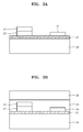
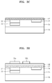
- FIGS. 3A through 3D are diagrams illustrating an example embodiment of a method of manufacturing the graphene electronic device 100 shown in FIGS. 1A and 1B .
- a semiconductor layer 32, a first conductive layer 33, and a second conductive layer 34 are formed on substrate 30 and 31.
- the substrate 30 and 31 may be formed of various substrate materials.
- the substrate 30 and 31 may be a silicon substrate 30 on which a silicon oxide layer 31 is formed, a glass substrate, a SiC substrate, a GaN substrate, etc.
- a semiconductor material layer is formed on the substrate 30 and 31 and patterned to form the semiconductor layer 32.
- a conductive material layer is formed on the semiconductor layer 32 and the substrate 30 and 31, patterned to form the first conductive layer 33 and the second conductive layer 34.
- an insulating material is formed on the substrate 30 and 31, the semiconductor layer 32, the first conductive layer 33, and the second conductive layer 34 to form an intermediate layer 35.
- the intermediate layer 35 may be formed of an insulating material such as polymer, silicon oxide, silicon nitride, etc.
- a support structure 36 is formed on the intermediate layer 35.
- the support structure 36 is formed to support a device in post processes, and may be selectively omitted.
- the substrate 30 and 31 are removed.
- the substrate 30 and 31 may be removed in various ways. For example, if the substrate 30 and 31 include silicon/silicon oxide, then the silicon oxide may be removed by etching.
- an interface area of the substrate 30 and 31 may be divided by irradiating laser in a laser lift-off (LLO) process.
- the substrate 30 and 31 may be used in a state where a material such as SiO:H, SiN:H, a-Si:H, AlO, ZnO, MgO, or GaN is formed on a transparent substrate such as glass by a plasma-enhanced CVD (PECVD) method.
- PECVD plasma-enhanced CVD
- a gate insulating layer 38 is formed on the graphene layer 37.
- a conductive material is then applied on the gate insulating layer 38, and patterned to form a first gate 39a and a second gate 39b.
- the graphene electronic device may be used to form various kinds of electronic devices according to a gate structure formed on a graphene layer.
- FIG. 4 is a cross-sectional view of an example embodiment of a ferroelectric random access memory (FRAM) device including graphene.
- FRAM ferroelectric random access memory
- an intermediate layer 41 is formed on a support structure 40, a first conductive layer 42 and a semiconductor layer 43 are formed on a first region of the intermediate layer 41, and a second conductive layer 44 is formed on a second region of the intermediate layer 41.
- a graphene layer 45 is formed on the intermediate layer 41, the semiconductor layer 43, and the second conductive layer 44.
- First and second gate structures are formed on the graphene layer 45.
- the first gate structure includes a ferroelectric layer 46 and a first gate 48.
- the second gate structure includes a ferroelectric layer 47 and a second gate 49.
- the first gate structure is formed on the graphene layer 45 to correspond to the first region of the intermediate layer 51
- the second gate structure is formed on the graphene layer 45 in a space between the first and second regions of the intermediate layer 41.
- the ferroelectric layers 46 and 47 may be formed of a ferroelectric material such as lead zirconate titanate (PZT), BaTiO 3 , polyvinylidene difluoride (PVDF), etc.
- the memory device having the structure shown in FIG. 4 may be a 2-bit/cell memory device.
- FIG. 5 is a cross-sectional view of an example embodiment of a flash memory device including graphene.
- the flash memory device includes an intermediate layer 51 formed on a support structure 50, a first conductive layer 52 and a semiconductor layer 53 formed on a first region of the intermediate layer 51, and a second conductive layer 54 formed on a second region of the intermediate layer 51.
- a graphene layer 55 is formed on the intermediate layer 51, the semiconductor layer 53, and the second conductive layer 54.
- a first gate structure and a second gate structure are formed on the graphene layer 55.
- the first gate structure is formed on the graphene layer 55 to correspond to the first region of the intermediate layer 51.
- the second gate structure is formed on the graphene layer 55 in a space between the first and second regions of the intermediate layer 51.
- the first gate structure includes a first tunneling oxide layer 561, a first floating gate 562, a first blocking oxide layer 563, and a first gate 564.
- the second gate structure includes a second tunneling oxide layer 571, a second floating gate 572, a second blocking oxide layer 573, and a second gate 574.
- the memory device shown in FIG. 5 may be a 2-bit/cell flash memory device.
- FIG. 6 is a cross-sectional view of an example embodiment of a hybrid-type memory device including graphene.
- the hybrid-type memory device includes an intermediate layer 61 formed on a support structure 60, a first conductive layer 62 and a semiconductor layer 63 formed on a first region of the intermediate layer 61, and a second conductive layer 64 formed on a second region of the intermediate layer 61.
- a graphene layer 65 is formed on the intermediate layer 61, the semiconductor layer 63, and the second conductive layer 64.
- a first gate structure and a second gate structure are formed on the graphene layer 65.
- the first gate structure is formed on the graphene layer 65 to correspond to the first region of the intermediate layer 61.
- the second gate structure is formed in a space between the first and second regions of the intermediate layer 61.
- the first gate structure includes a tunneling oxide layer 661, a floating gate 662, a blocking oxide layer 663, and a first gate 664.
- the second gate structure includes a ferroelectric layer 671 and a second gate 672.
- the first gate structure is a flash memory region
- the second gate structure is a ferroelectric memory region.
- the first gate structure may be formed as a ferroelectric memory region including a ferroelectric layer and a gate
- the second gate structure may be formed as a flash memory region.
- graphene electronic devices having improved electrical characteristics by using graphene may be formed. Also, switching devices having characteristics of both graphene transistors and graphene diodes may be formed. In addition, memory devices having characteristics of both graphene transistors and graphene diodes may be formed.
Landscapes
- Engineering & Computer Science (AREA)
- Chemical & Material Sciences (AREA)
- Nanotechnology (AREA)
- Physics & Mathematics (AREA)
- Mathematical Physics (AREA)
- Theoretical Computer Science (AREA)
- Crystallography & Structural Chemistry (AREA)
- Thin Film Transistor (AREA)
Abstract
Description
- Example embodiments relate to graphene electronic devices and methods of manufacturing the same.
- Rapidly, semiconductor devices formed on silicon substrates have become more highly integrated to have a relatively high performance. However, there is a limitation in improving the performance of semiconductor devices due to characteristics of silicon itself and in manufacturing processes. Accordingly, research has been conducted into next generation devices that may overcome the limitations of conventional semiconductor devices having silicon substrates.
- Graphene, a graphite monoatomic layer, is being considered as a next generation material due to its superior electrical and mechanical properties. Graphene is a material in which carbon atoms are connected as a hexagon in a plane, and has a relatively small thickness corresponding to a monoatomic layer. Thus, graphene conducts electricity about a hundred times faster than polycrystalline silicon that is mainly used as a semiconductor, and theoretically has an electron mobility of about 200,000 cm2/Vs, 20 m2/Vs. In addition, it is known that graphene may conduct electricity about a hundred times more than copper, and thus, graphene is considered as a basic material of electronic devices.
- In particular, graphene is a zero gap semiconductor material, and thus, if a graphene nanoribbon (GNR) is manufactured to have a channel width of about 10 nm or less, a band gap is generated due to a size effect. Thus, a field effect transistor (FET) capable of operating at about room temperature may be manufactured.
- Conventionally, graphene is grown on a metal thin film formed of copper (Cu) or nickel (Ni) by a chemical vapor deposition (CVD) method, and then, may be transferred onto an insulating thin film.
- Example embodiments provide graphene switching devices including graphene field effect transistors (FETs) and graphene diodes.
- Example embodiments provide graphene memory devices formed by combining graphene FETs and graphene diodes.
- Additional aspects will be set forth in part in the description which follows and, in part, will be apparent from the description, or may be learned by practice of the presented embodiments.
- At least one example embodiment provides a graphene electronic device. According to at least this example embodiment, the graphene electronic device includes: a first conductive layer and a semiconductor layer on a first region of an intermediate layer; a second conductive layer on a second region of the intermediate layer; a graphene layer on the intermediate layer, the semiconductor layer, and the second conductive layer; and a first gate structure and a second gate structure on the graphene layer.
- According to at least some example embodiments, the first gate structure may be formed on the graphene layer to correspond to the first region of the intermediate layer. The second gate structure may by formed on the graphene layer in a space between the first region and the second region of the intermediate layer. The intermediate layer may be formed on a support structure.
- According to at least some example embodiments, the first gate structure may include a gate insulating layer and a first gate. The second gate structure may include the gate insulating layer and a second gate.
- According to at least some example embodiments, the first gate structure may include a first ferroelectric layer and a first gate. The second gate structure may include a second ferroelectric layer and a second gate.
- According to at least some example embodiments, the first gate structure may include a first tunneling oxide layer, a first floating gate, a first blocking oxide layer, and a first gate. The second gate structure may include a second tunneling oxide layer, a second floating gate, a second blocking oxide layer, and a second gate.
- At least one other example embodiment provides a method of forming a graphene electronic device. According to at least this example embodiment, the method includes: forming a semiconductor layer, a first conductive layer, and a second conductive layer on a substrate; forming an intermediate layer on the substrate, the semiconductor layer, the first conductive layer, and the second conductive layer; removing the substrate, and forming a graphene layer on the intermediate layer, the semiconductor layer, and the second conductive layer; and forming a first gate structure and a second gate structure on the graphene layer.
- According to at least some example embodiments, the method of forming a graphene electronic device may further include: forming a support structure on the intermediate layer, after forming the intermediate layer.
- In at least one example embodiment, the substrate may include silicon and a silicon oxide layer, and the substrate may be removed by etching the silicon oxide layer. In at least one other example embodiment, the substrate may include a transparent substrate, and the substrate may be removed by a laser lift-off process.
- The graphene layer may be formed on a catalyst layer by a pyrolisis method or a chemical vapor deposition (CVD) method, after forming the catalyst layer on the intermediate layer.
- At least one other example embodiment provides a graphene electronic device. According to at least this example embodiment, the graphene electronic device includes: a graphene transistor having a channel including a graphene layer and an electrode including a semiconductor layer; and a graphene tunable diode having a diode region including the graphene layer and the semiconductor layer.
- According to at least some example embodiments, the graphene transistor may include: a first conductive layer and the semiconductor layer on a first region of an intermediate layer; a second conductive layer on a second region of the intermediate layer; the graphene layer on the intermediate layer, the semiconductor layer, and the second conductive layer; and a gate structure on the graphene layer.
- The graphene tunable diode may include: the semiconductor layer on a first region of an intermediate layer; the graphene layer on the intermediate layer and the semiconductor layer; and a gate structure on the graphene layer corresponding to the first region of the intermediate layer.
- According to at least some example embodiments, the device may further include: a first conductive layer and the semiconductor layer on a first region of an intermediate layer; a second conductive layer on a second region of the intermediate layer; the graphene layer on the intermediate layer, the semiconductor layer, and the second conductive layer; and a first gate structure and a second gate structure on the graphene layer.
- The device may further include a first gate structure corresponding to the graphene transistor; and a second gate structure corresponding to the graphene tunable diode.
- According to at least some example embodiments, the gate structure may include a tunneling oxide layer, a floating gate, a blocking oxide layer, and a gate, or the gate structure may include a ferroelectric layer and a gate.
- These and/or other aspects will become apparent and more readily appreciated from the following description of example embodiments, taken in conjunction with the accompanying drawings in which:
-
FIG. 1A is a cross-sectional view of a graphene electronic device according to an example embodiment; -
FIG. 1B is a schematic plan view of the graphene electronic device ofFIG. 1 ; -
FIG. 2 is a graph showing electrical characteristics of the graphene electronic device according to an example embodiment; -
FIGS. 3A through 3D are diagrams illustrating an example embodiment of a method of manufacturing the graphene electronic device shown inFIG. 1A ; -
FIG. 4 is a cross-sectional view of an example embodiment of a ferroelectric memory device including graphene; -
FIG. 5 is a cross-sectional view of an example embodiment of a flash memory device including graphene; and -
FIG. 6 is a cross-sectional view of an example embodiment of a hybrid-type memory device including graphene. - Example embodiments will now be described more fully with reference to the accompanying drawings, in which some example embodiments are shown. In the drawings, the thicknesses of layers and regions are exaggerated for clarity. Like reference numerals in the drawings denote like elements.
- Detailed illustrative embodiments are disclosed herein. However, specific structural and functional details disclosed herein are merely representative for purposes of describing example embodiments. Example embodiments may be embodied in many alternate forms and should not be construed as limited to only those set forth herein.
- It should be understood, however, that there is no intent to limit this disclosure to the particular example embodiments disclosed. On the contrary, example embodiments are to cover all modifications, equivalents, and alternatives falling within the scope of the invention. Like numbers refer to like elements throughout the description of the figures.
- It will be understood that, although the terms first, second, etc. may be used herein to describe various elements, these elements should not be limited by these terms. These terms are only used to distinguish one element from another. For example, a first element could be termed a second element, and, similarly, a second element could be termed a first element, without departing from the scope of this disclosure. As used herein, the term "and/or," includes any and all combinations of one or more of the associated listed items.
- It will be understood that when an element is referred to as being "connected," or "coupled," to another element, it can be directly connected or coupled to the other element or intervening elements may be present. In contrast, when an element is referred to as being "directly connected," or "directly coupled," to another element, there are no intervening elements present. Other words used to describe the relationship between elements should be interpreted in a like fashion (e.g., "between," versus "directly between," "adjacent," versus "directly adjacent," etc.).
- The terminology used herein is for the purpose of describing particular embodiments only and is not intended to be limiting. As used herein, the singular forms "a," "an," and "the," are intended to include the plural forms as well, unless the context clearly indicates otherwise. It will be further understood that the terms "comprises," "comprising," "includes," and/or "including," when used herein, specify the presence of stated features, integers, steps, operations, elements, and/or components, but do not preclude the presence or addition of one or more other features, integers, steps, operations, elements, components, and/or groups thereof.
- It should also be noted that in some alternative implementations, the functions/acts noted may occur out of the order noted in the figures. For example, two figures shown in succession may in fact be executed substantially concurrently or may sometimes be executed in the reverse order, depending upon the functionality/acts involved.
- Various example embodiments of the present invention will now be described more fully with reference to the accompanying drawings in which some example embodiments of the invention are shown. In the drawings, the thicknesses of layers and regions are exaggerated for clarity.
-
FIG. 1A is a cross-sectional view of a grapheneelectronic device 100 according to an example embodiment. In addition,FIG. 1B is a schematic plan view of the grapheneelectronic device 100 shown inFIG. 1A. FIG. 1A is a cross-sectional view taken along line m1-m2 ofFIG. 1B . - Referring to
FIGS. 1A and 1B , the grapheneelectronic device 100 includes anintermediate layer 11 formed on asupport structure 10, a firstconductive layer 12 and asemiconductor layer 13 formed on a first region of theintermediate layer 11, and a secondconductive layer 14 formed on a second region of theintermediate layer 11. In addition, agraphene layer 15 is formed on theintermediate layer 11, thesemiconductor layer 13, and the secondconductive layer 14. First and second gate structures are formed on thegraphene layer 15. The first gate structure includes agate insulating layer 16 and afirst gate 17. The second gate structure includes thegate insulating layer 16 and asecond gate 18. On thegraphene layer 15, the first gate structure is formed corresponding to the first region of theintermediate layer 11, and the second gate structure is formed in a space between the first and second regions of theintermediate layer 11. - The graphene electronic device according to at least this example embodiment may be configured to perform functions of a graphene transistor and/or a graphene diode. Referring to
FIG. 1A , thesemiconductor layer 13 and thegraphene layer 15 may be a diode region functioning as a graphene tunable diode according to a voltage applied via thefirst gate 17. In addition, regarding the graphene transistor function, the firstconductive layer 12 and thesemiconductor layer 13 inFIG. 1A may be a source electrode, the secondconductive layer 14 may be a drain electrode, thegraphene layer 15 may be a channel region, and thesecond gate 18 may be a gate electrode. - Materials forming each of the layers in the graphene electronic device according to at least this example embodiment are described below.
- The
support structure 10 supports each of the layers of the graphene electronic device formed thereon, and may be formed in manufacturing processes for processing stability. Thesupport structure 10 may be formed of various materials, for example, a semiconductor substrate such as a Si substrate that is used as a substrate of a semiconductor device, a polymer substrate, an adhesive tape, etc. Thesupport structure 10 may include a material having relatively high attachability to theintermediate layer 11, and if necessary, thesupport structure 10 may be formed of the same or substantially the same material as that of theintermediate layer 11. - The
intermediate layer 11 may be formed of a polymer material, or a material having an insulating property. Theintermediate layer 11 may be a protective layer that protects thegraphene layer 15 and the first and secondconductive layers electronic device 100. The firstconductive layer 12, the secondconductive layer 14, thefirst gate 17, and thesecond gate 18 may be formed of a conductive material such as metal, a metal alloy, conductive metal oxide, conductive polymer, etc. - The
semiconductor layer 13 may be formed of a semiconductor material, for example, a material including silicon (Si), amorphous silicon (a-Si), zinc-oxide (ZnO), gallium-indium-zinc-oxide (GalnZnOx), hafnium-indium-zinc-oxide (HflnZnOx), gallium-nitride (GaN), gallium-arsenic (GaAs), aluminum-gallium-arsenic (AlGaAs), etc., and may be formed to have a single or multi-layer structure. In addition, thesemiconductor layer 13 may include a layer doped with impurities, for example, a-Si/n-type Si structure. - The
gate insulating layer 16 may be formed of an insulating material such as that formed in a semiconductor device. For example, thegate insulating layer 16 may be silicon oxide, silicon nitride, aluminum oxide, hafnium oxide, zinc oxide, magnesium oxide, etc. - The
graphene layer 15 may be formed by using various methods. For example, to form thegraphene layer 15, a catalyst layer including nickel (Ni), copper (Cu), cobalt (Co), platinum (Pt), or ruthenium (Ru) may be formed first, and thegraphene layer 15 may be formed on the catalyst layer, for example, by a pyrolysis method or a chemical vapor deposition (CVD) method. -
FIG. 2 is a graph schematically showing example electrical characteristics of the grapheneelectronic device 100 shown inFIGS. 1A and 1B . - Referring to
FIG. 2 , an electric current according to a voltage applied via the firstconductive layer 12 and the secondconductive layer 14 in a state where a voltage is not applied to thefirst gate 17 and the second gate 18 (Vg1=1 and Vg2=0) follows graph 1. - When the voltage is not applied to the first gate 17 (Vg=0) and a voltage is applied to the second gate 18 (Vg2>0), the electric current increases according to the transistor characteristics illustrating graph 2. On the other hand, when a voltage is applied to the first gate 17 (Vg>0) and a voltage is not applied to the second gate 18 (Vg2=0), a turn-on voltage increases due to tunable diode characteristics as shown in
graph 3. If the voltage is applied to both of thefirst gate 17 and the second gate 18 (Vg>0 and Vg2>0), the electric current and the turn-on voltage both increase as shown in graph 4 according to the transistor characteristics and the tunable diode characteristics. - Hereinafter, an example embodiment of a method of manufacturing a graphene electronic device is described with reference to
FIGS. 3A through 3D . -
FIGS. 3A through 3D are diagrams illustrating an example embodiment of a method of manufacturing the grapheneelectronic device 100 shown inFIGS. 1A and 1B . - Referring to
FIG. 3A , asemiconductor layer 32, a first conductive layer 33, and a secondconductive layer 34 are formed onsubstrate substrate substrate silicon substrate 30 on which asilicon oxide layer 31 is formed, a glass substrate, a SiC substrate, a GaN substrate, etc. - A semiconductor material layer is formed on the
substrate semiconductor layer 32. A conductive material layer is formed on thesemiconductor layer 32 and thesubstrate conductive layer 34. - Referring to
FIG. 3B , an insulating material is formed on thesubstrate semiconductor layer 32, the first conductive layer 33, and the secondconductive layer 34 to form anintermediate layer 35. Theintermediate layer 35 may be formed of an insulating material such as polymer, silicon oxide, silicon nitride, etc. - After forming the
intermediate layer 35, asupport structure 36 is formed on theintermediate layer 35. Thesupport structure 36 is formed to support a device in post processes, and may be selectively omitted. - Referring to
FIG. 3C , thesubstrate substrate substrate substrate substrate graphene layer 37 is then formed on a portion from which thesubstrate - Referring to
FIG. 3D , agate insulating layer 38 is formed on thegraphene layer 37. A conductive material is then applied on thegate insulating layer 38, and patterned to form afirst gate 39a and asecond gate 39b. - The graphene electronic device according to at least some example embodiments may be used to form various kinds of electronic devices according to a gate structure formed on a graphene layer.
-
FIG. 4 is a cross-sectional view of an example embodiment of a ferroelectric random access memory (FRAM) device including graphene. - Referring to
FIG. 4 , anintermediate layer 41 is formed on asupport structure 40, a firstconductive layer 42 and asemiconductor layer 43 are formed on a first region of theintermediate layer 41, and a secondconductive layer 44 is formed on a second region of theintermediate layer 41. Agraphene layer 45 is formed on theintermediate layer 41, thesemiconductor layer 43, and the secondconductive layer 44. First and second gate structures are formed on thegraphene layer 45. The first gate structure includes aferroelectric layer 46 and afirst gate 48. The second gate structure includes aferroelectric layer 47 and asecond gate 49. In this example embodiment, the first gate structure is formed on thegraphene layer 45 to correspond to the first region of theintermediate layer 51, and the second gate structure is formed on thegraphene layer 45 in a space between the first and second regions of theintermediate layer 41. The ferroelectric layers 46 and 47 may be formed of a ferroelectric material such as lead zirconate titanate (PZT), BaTiO3, polyvinylidene difluoride (PVDF), etc. The memory device having the structure shown inFIG. 4 may be a 2-bit/cell memory device. -
FIG. 5 is a cross-sectional view of an example embodiment of a flash memory device including graphene. - Referring to
FIG. 5 , the flash memory device includes anintermediate layer 51 formed on asupport structure 50, a firstconductive layer 52 and a semiconductor layer 53 formed on a first region of theintermediate layer 51, and a secondconductive layer 54 formed on a second region of theintermediate layer 51. Agraphene layer 55 is formed on theintermediate layer 51, the semiconductor layer 53, and the secondconductive layer 54. A first gate structure and a second gate structure are formed on thegraphene layer 55. The first gate structure is formed on thegraphene layer 55 to correspond to the first region of theintermediate layer 51. The second gate structure is formed on thegraphene layer 55 in a space between the first and second regions of theintermediate layer 51. The first gate structure includes a firsttunneling oxide layer 561, a first floatinggate 562, a first blocking oxide layer 563, and afirst gate 564. The second gate structure includes a secondtunneling oxide layer 571, a second floatinggate 572, a secondblocking oxide layer 573, and asecond gate 574. The memory device shown inFIG. 5 may be a 2-bit/cell flash memory device. -
FIG. 6 is a cross-sectional view of an example embodiment of a hybrid-type memory device including graphene. - Referring to
FIG. 6 , the hybrid-type memory device includes anintermediate layer 61 formed on asupport structure 60, a firstconductive layer 62 and asemiconductor layer 63 formed on a first region of theintermediate layer 61, and a secondconductive layer 64 formed on a second region of theintermediate layer 61. Agraphene layer 65 is formed on theintermediate layer 61, thesemiconductor layer 63, and the secondconductive layer 64. A first gate structure and a second gate structure are formed on thegraphene layer 65. The first gate structure is formed on thegraphene layer 65 to correspond to the first region of theintermediate layer 61. The second gate structure is formed in a space between the first and second regions of theintermediate layer 61. The first gate structure includes atunneling oxide layer 661, a floatinggate 662, a blocking oxide layer 663, and afirst gate 664. The second gate structure includes aferroelectric layer 671 and asecond gate 672. In the memory device shown inFIG. 6 , the first gate structure is a flash memory region, and the second gate structure is a ferroelectric memory region. However, the first gate structure may be formed as a ferroelectric memory region including a ferroelectric layer and a gate, and the second gate structure may be formed as a flash memory region. - According to at least some example embodiments, graphene electronic devices having improved electrical characteristics by using graphene may be formed. Also, switching devices having characteristics of both graphene transistors and graphene diodes may be formed. In addition, memory devices having characteristics of both graphene transistors and graphene diodes may be formed.
- It should be understood that the example embodiments described therein should be considered in a descriptive sense only and not for purposes of limitation. Descriptions of features or aspects within each embodiment should typically be considered as available for other similar features or aspects in other embodiments.
Claims (15)
- A graphene electronic device comprising:a first conductive layer and a semiconductor layer on a first region of an intermediate layer;a second conductive layer on a second region of the intermediate layer;a graphene layer on the intermediate layer, the semiconductor layer, and the second conductive layer; anda first gate structure and a second gate structure on the graphene layer.
- The device of claim 1, wherein the first gate structure corresponds to the first region of the intermediate layer.
- The device of claim 1 or 2, wherein the second gate structure corresponds to a space between the first region and the second region of the intermediate layer.
- The device of any preceding claim, wherein the intermediate layer is on a support structure.
- The device of any preceding claim, wherein the first gate structure includes a first ferroelectric layer and a first gate.
- The device of any preceding claim, wherein the second gate structure includes a second ferroelectric layer and a second gate.
- The device of any of claims 1 to 4, wherein the first gate structure includes a first tunneling oxide layer, a first floating gate, a first blocking oxide layer, and a first gate.
- The device of any of claims 1 to 4 or 7, wherein the second gate structure includes a second tunneling oxide layer, a second floating gate, a second blocking oxide layer, and a second gate.
- A graphene electronic device according to any preceding claim, comprising:a graphene transistor having a channel including the graphene layer and an electrode including the semiconductor layer; anda graphene tunable diode having a diode region including the graphene layer and the semiconductor layer.
- The device of claim 9, wherein:the first gate structure corresponds to the graphene transistor; andthe second gate structure corresponds to the graphene tunable diode.
- The device of claim 9 or 10, wherein the graphene transistor comprises:the first conductive layer and the semiconductor layer on a first region of an intermediate layer;the second conductive layer on a second region of the intermediate layer;the graphene layer on the intermediate layer, the semiconductor layer, and the second conductive layer; andthe first gate structure on the graphene layer.
- The device of claim 9, 10 or 11, wherein the graphene tunable diode comprises:the semiconductor layer on the first region of an intermediate layer;the graphene layer on the intermediate layer and the semiconductor layer; andthe second gate structure on the graphene layer corresponding to the first region of the intermediate layer.
- A method of forming a graphene electronic device, the method comprising:forming a semiconductor layer, a first conductive layer, and a second conductive layer on a substrate;forming an intermediate layer on the substrate, the semiconductor layer, the first conductive layer, and the second conductive layer;forming a graphene layer on the intermediate layer, the semiconductor layer, and the second conductive layer; andforming a first gate structure and a second gate structure on the graphene layer,and optionally further comprising forming a support structure on the intermediate layer.
- The method of claim 13, further comprising:removing the substrate; preferably wherein either(a) the substrate includes silicon and a silicon oxide layer, and wherein the substrate is removed by etching the silicon oxide layer; or.(b) wherein the substrate includes a transparent substrate, and wherein the substrate is removed by a laser lift-off process.
- The device of claim 13 or 14, wherein the graphene layer is formed on a catalyst layer by a pyrolisis method or a chemical vapor deposition (CVD) method.
Applications Claiming Priority (1)
| Application Number | Priority Date | Filing Date | Title |
|---|---|---|---|
| KR1020130002223A KR101919426B1 (en) | 2013-01-08 | 2013-01-08 | Graphene electronic device and Manufacturing method of the same |
Publications (3)
| Publication Number | Publication Date |
|---|---|
| EP2752880A2 true EP2752880A2 (en) | 2014-07-09 |
| EP2752880A3 EP2752880A3 (en) | 2017-10-18 |
| EP2752880B1 EP2752880B1 (en) | 2025-04-02 |
Family
ID=49920134
Family Applications (1)
| Application Number | Title | Priority Date | Filing Date |
|---|---|---|---|
| EP14150063.7A Active EP2752880B1 (en) | 2013-01-08 | 2014-01-02 | Graphene electronic devices and methods of manufacturing the same |
Country Status (4)
| Country | Link |
|---|---|
| US (1) | US9142639B2 (en) |
| EP (1) | EP2752880B1 (en) |
| KR (1) | KR101919426B1 (en) |
| CN (1) | CN103915496B (en) |
Cited By (3)
| Publication number | Priority date | Publication date | Assignee | Title |
|---|---|---|---|---|
| EP3136445A1 (en) * | 2015-08-25 | 2017-03-01 | Emberion Oy | A method for forming apparatus comprising two dimensional material |
| WO2022238425A1 (en) * | 2021-05-14 | 2022-11-17 | Paragraf Limited | A method of manufacturing a light-emitting device and a light-emitting device |
| EP3344980B1 (en) * | 2015-09-02 | 2023-07-26 | Cardea Bio, Inc. | Chemically-sensitive field effect transistors, systems and methods for using the same |
Families Citing this family (5)
| Publication number | Priority date | Publication date | Assignee | Title |
|---|---|---|---|---|
| KR101910579B1 (en) * | 2012-10-29 | 2018-10-22 | 삼성전자주식회사 | Graphene switching device having tunable barrier |
| KR102237826B1 (en) * | 2014-07-18 | 2021-04-08 | 삼성전자주식회사 | Graphene device, methods of manufacturing and operating the same, and electronic apparatus including graphene device |
| KR102412965B1 (en) * | 2014-12-30 | 2022-06-24 | 삼성전자주식회사 | Electronic device having two dimensional material layer and method of manufacturing the electronic device using inkjet printing |
| US10319426B2 (en) | 2017-05-09 | 2019-06-11 | Micron Technology, Inc. | Semiconductor structures, memory cells and devices comprising ferroelectric materials, systems including same, and related methods |
| CN110911409B (en) * | 2018-09-18 | 2022-05-03 | 联华电子股份有限公司 | Non-volatile memory and forming method thereof |
Family Cites Families (26)
| Publication number | Priority date | Publication date | Assignee | Title |
|---|---|---|---|---|
| US7345296B2 (en) * | 2004-09-16 | 2008-03-18 | Atomate Corporation | Nanotube transistor and rectifying devices |
| US7732859B2 (en) * | 2007-07-16 | 2010-06-08 | International Business Machines Corporation | Graphene-based transistor |
| JP2009277803A (en) | 2008-05-13 | 2009-11-26 | Fujitsu Ltd | Semiconductor device, method for manufacturing the semiconductor device and transistor |
| US7858989B2 (en) * | 2008-08-29 | 2010-12-28 | Globalfoundries Inc. | Device and process of forming device with device structure formed in trench and graphene layer formed thereover |
| US7993986B2 (en) * | 2008-08-29 | 2011-08-09 | Advanced Micro Devices, Inc. | Sidewall graphene devices for 3-D electronics |
| WO2010036210A1 (en) | 2008-09-23 | 2010-04-01 | National University Of Singapore | Graphene memory cell and fabrication methods thereof |
| JP5453045B2 (en) * | 2008-11-26 | 2014-03-26 | 株式会社日立製作所 | Substrate on which graphene layer is grown and electronic / optical integrated circuit device using the same |
| KR101156620B1 (en) * | 2009-04-08 | 2012-06-14 | 한국전자통신연구원 | Field effect transistor having graphene channel layer |
| JP5744861B2 (en) * | 2009-06-17 | 2015-07-08 | ザ、リージェンツ、オブ、ザ、ユニバーシティー、オブ、ミシガン | Photodiode and other sensor structures in flat panel x-ray imagers and methods for improving the topological uniformity of photodiodes and other sensor structures in flat panel x-ray imagers using thin film electronics |
| US8409366B2 (en) * | 2009-06-23 | 2013-04-02 | Oki Data Corporation | Separation method of nitride semiconductor layer, semiconductor device, manufacturing method thereof, semiconductor wafer, and manufacturing method thereof |
| US8445893B2 (en) | 2009-07-21 | 2013-05-21 | Trustees Of Columbia University In The City Of New York | High-performance gate oxides such as for graphene field-effect transistors or carbon nanotubes |
| US9362364B2 (en) * | 2009-07-21 | 2016-06-07 | Cornell University | Transfer-free batch fabrication of single layer graphene devices |
| KR101694877B1 (en) * | 2009-10-16 | 2017-01-11 | 삼성전자주식회사 | Graphene device and method of manufacturing the same |
| US8673703B2 (en) * | 2009-11-17 | 2014-03-18 | International Business Machines Corporation | Fabrication of graphene nanoelectronic devices on SOI structures |
| US8410474B2 (en) * | 2010-01-21 | 2013-04-02 | Hitachi, Ltd. | Graphene grown substrate and electronic/photonic integrated circuits using same |
| US8890277B2 (en) * | 2010-03-15 | 2014-11-18 | University Of Florida Research Foundation Inc. | Graphite and/or graphene semiconductor devices |
| US8445320B2 (en) * | 2010-05-20 | 2013-05-21 | International Business Machines Corporation | Graphene channel-based devices and methods for fabrication thereof |
| US9281385B2 (en) * | 2010-06-18 | 2016-03-08 | Samsung Electronics Co., Ltd. | Semiconducting graphene composition, and electrical device including the same |
| KR101718961B1 (en) * | 2010-11-05 | 2017-03-23 | 삼성전자주식회사 | Semiconductor device comprising Graphene and method of manufacturing the same |
| JP5629570B2 (en) | 2010-12-27 | 2014-11-19 | 株式会社日立製作所 | Circuit device in which graphene film and metal electrode are electrically joined |
| KR101920712B1 (en) * | 2011-08-26 | 2018-11-22 | 삼성전자주식회사 | Graphene switching devece including tunable barrier |
| KR101878746B1 (en) * | 2011-12-06 | 2018-07-17 | 삼성전자주식회사 | Hexagonal boron nitride sheet, process for preparing the sheet and electronic device comprising the sheet |
| KR102037469B1 (en) * | 2012-01-02 | 2019-10-28 | 삼성전자주식회사 | Graphene electronic device and manufacturing method thereof |
| US8735271B2 (en) * | 2012-08-24 | 2014-05-27 | International Business Machines Corporation | Gate tunable tunnel diode |
| US8932919B2 (en) * | 2012-11-21 | 2015-01-13 | International Business Machines Corporation | Vertical stacking of graphene in a field-effect transistor |
| US8766258B1 (en) * | 2012-12-12 | 2014-07-01 | International Business Machines Corporation | Authentication using graphene based devices as physical unclonable functions |
-
2013
- 2013-01-08 KR KR1020130002223A patent/KR101919426B1/en active Active
- 2013-08-26 US US13/975,680 patent/US9142639B2/en active Active
- 2013-11-01 CN CN201310534898.6A patent/CN103915496B/en active Active
-
2014
- 2014-01-02 EP EP14150063.7A patent/EP2752880B1/en active Active
Non-Patent Citations (1)
| Title |
|---|
| None |
Cited By (5)
| Publication number | Priority date | Publication date | Assignee | Title |
|---|---|---|---|---|
| EP3136445A1 (en) * | 2015-08-25 | 2017-03-01 | Emberion Oy | A method for forming apparatus comprising two dimensional material |
| WO2017032850A1 (en) * | 2015-08-25 | 2017-03-02 | Emberion Oy | A method for forming apparatus comprising two dimensional material |
| US10396180B2 (en) | 2015-08-25 | 2019-08-27 | Emberion Oy | Method for forming apparatus comprising two dimensional material |
| EP3344980B1 (en) * | 2015-09-02 | 2023-07-26 | Cardea Bio, Inc. | Chemically-sensitive field effect transistors, systems and methods for using the same |
| WO2022238425A1 (en) * | 2021-05-14 | 2022-11-17 | Paragraf Limited | A method of manufacturing a light-emitting device and a light-emitting device |
Also Published As
| Publication number | Publication date |
|---|---|
| KR20140090021A (en) | 2014-07-16 |
| KR101919426B1 (en) | 2018-11-19 |
| EP2752880A3 (en) | 2017-10-18 |
| CN103915496B (en) | 2019-01-11 |
| US20140191198A1 (en) | 2014-07-10 |
| EP2752880B1 (en) | 2025-04-02 |
| CN103915496A (en) | 2014-07-09 |
| US9142639B2 (en) | 2015-09-22 |
Similar Documents
| Publication | Publication Date | Title |
|---|---|---|
| US9142639B2 (en) | Graphene electronic devices and methods of manufacturing the same | |
| US10872973B2 (en) | Semiconductor structures with two-dimensional materials | |
| US11152209B2 (en) | Forming semiconductor structures with two-dimensional materials | |
| US12426344B2 (en) | Method of manufacturing semiconductor device | |
| US9337332B2 (en) | III-Nitride insulating-gate transistors with passivation | |
| CN207303109U (en) | Electronic device | |
| JP6251071B2 (en) | Semiconductor device | |
| US9318593B2 (en) | Forming enhancement mode III-nitride devices | |
| CN104218079B (en) | Semiconductor device and method of manufacturing semiconductor device | |
| CN104871319B (en) | Semiconductor structure and groove formation etching technology | |
| US11049961B2 (en) | High electron mobility transistor and methods for manufacturing the same | |
| JP6305596B1 (en) | Semiconductor device and manufacturing method thereof | |
| WO2009113612A1 (en) | Semiconductor device | |
| JP5487615B2 (en) | Field effect semiconductor device and manufacturing method thereof | |
| EP2348531A2 (en) | Thin film transistor and method of manufacturing the same | |
| US20150364589A1 (en) | Graphene-metal bonding structure, method of manufacturing the same, and semiconductor device having the graphene-metal bonding structure | |
| CN103548127A (en) | Semiconductor device and manufacturing method thereof | |
| US10460944B2 (en) | Fully depleted semiconductor on insulator transistor with enhanced back biasing tunability | |
| WO2009119103A1 (en) | Semiconductor substrate, semiconductor device and semiconductor device manufacturing method | |
| JP2012129511A (en) | Semiconductor device and method of manufacturing the same | |
| CN104051516A (en) | HEMT semiconductor device and a process of forming the same | |
| WO2019107411A1 (en) | Tunneling field effect transistor | |
| CN113875015A (en) | Diode, diode manufacturing method, and electrical equipment | |
| JP5208439B2 (en) | Nitride semiconductor device | |
| JP2014203962A (en) | Semiconductor device and method of manufacturing the same |
Legal Events
| Date | Code | Title | Description |
|---|---|---|---|
| 17P | Request for examination filed |
Effective date: 20140102 |
|
| AK | Designated contracting states |
Kind code of ref document: A2 Designated state(s): AL AT BE BG CH CY CZ DE DK EE ES FI FR GB GR HR HU IE IS IT LI LT LU LV MC MK MT NL NO PL PT RO RS SE SI SK SM TR |
|
| AX | Request for extension of the european patent |
Extension state: BA ME |
|
| PUAI | Public reference made under article 153(3) epc to a published international application that has entered the european phase |
Free format text: ORIGINAL CODE: 0009012 |
|
| PUAL | Search report despatched |
Free format text: ORIGINAL CODE: 0009013 |
|
| AK | Designated contracting states |
Kind code of ref document: A3 Designated state(s): AL AT BE BG CH CY CZ DE DK EE ES FI FR GB GR HR HU IE IS IT LI LT LU LV MC MK MT NL NO PL PT RO RS SE SI SK SM TR |
|
| AX | Request for extension of the european patent |
Extension state: BA ME |
|
| RIC1 | Information provided on ipc code assigned before grant |
Ipc: H01L 29/788 20060101ALI20170908BHEP Ipc: H01L 21/683 20060101ALI20170908BHEP Ipc: H01L 21/28 20060101ALI20170908BHEP Ipc: H01L 29/16 20060101ALI20170908BHEP Ipc: H01L 21/336 20060101ALI20170908BHEP Ipc: H01L 27/115 20170101ALI20170908BHEP Ipc: H01L 29/78 20060101ALI20170908BHEP Ipc: H01L 29/417 20060101ALI20170908BHEP Ipc: H01L 29/423 20060101ALI20170908BHEP Ipc: H01L 29/778 20060101AFI20170908BHEP |
|
| STAA | Information on the status of an ep patent application or granted ep patent |
Free format text: STATUS: REQUEST FOR EXAMINATION WAS MADE |
|
| R17P | Request for examination filed (corrected) |
Effective date: 20180418 |
|
| RBV | Designated contracting states (corrected) |
Designated state(s): AL AT BE BG CH CY CZ DE DK EE ES FI FR GB GR HR HU IE IS IT LI LT LU LV MC MK MT NL NO PL PT RO RS SE SI SK SM TR |
|
| STAA | Information on the status of an ep patent application or granted ep patent |
Free format text: STATUS: EXAMINATION IS IN PROGRESS |
|
| 17Q | First examination report despatched |
Effective date: 20200326 |
|
| P01 | Opt-out of the competence of the unified patent court (upc) registered |
Effective date: 20230519 |
|
| GRAP | Despatch of communication of intention to grant a patent |
Free format text: ORIGINAL CODE: EPIDOSNIGR1 |
|
| STAA | Information on the status of an ep patent application or granted ep patent |
Free format text: STATUS: GRANT OF PATENT IS INTENDED |
|
| RIC1 | Information provided on ipc code assigned before grant |
Ipc: H01L 29/417 20060101ALN20241016BHEP Ipc: H01L 21/28 20060101ALI20241016BHEP Ipc: H01L 21/683 20060101ALI20241016BHEP Ipc: H10B 51/30 20230101ALI20241016BHEP Ipc: H10B 41/30 20230101ALI20241016BHEP Ipc: H01L 29/423 20060101ALI20241016BHEP Ipc: H01L 29/16 20060101ALI20241016BHEP Ipc: H01L 29/788 20060101ALI20241016BHEP Ipc: H01L 21/336 20060101ALI20241016BHEP Ipc: H01L 29/778 20060101AFI20241016BHEP |
|
| INTG | Intention to grant announced |
Effective date: 20241025 |
|
| RIN1 | Information on inventor provided before grant (corrected) |
Inventor name: LEE, JOO-HO Inventor name: LEE, CHANG-SEUNG Inventor name: KIM, YONG-SUNG |
|
| GRAS | Grant fee paid |
Free format text: ORIGINAL CODE: EPIDOSNIGR3 |
|
| GRAA | (expected) grant |
Free format text: ORIGINAL CODE: 0009210 |
|
| STAA | Information on the status of an ep patent application or granted ep patent |
Free format text: STATUS: THE PATENT HAS BEEN GRANTED |
|
| AK | Designated contracting states |
Kind code of ref document: B1 Designated state(s): AL AT BE BG CH CY CZ DE DK EE ES FI FR GB GR HR HU IE IS IT LI LT LU LV MC MK MT NL NO PL PT RO RS SE SI SK SM TR |
|
| REG | Reference to a national code |
Ref country code: GB Ref legal event code: FG4D |
|
| REG | Reference to a national code |
Ref country code: IE Ref legal event code: FG4D |
|
| REG | Reference to a national code |
Ref country code: DE Ref legal event code: R096 Ref document number: 602014091745 Country of ref document: DE |
|
| REG | Reference to a national code |
Ref country code: NL Ref legal event code: FP |
|
| REG | Reference to a national code |
Ref country code: AT Ref legal event code: MK05 Ref document number: 1782195 Country of ref document: AT Kind code of ref document: T Effective date: 20250402 |
|
| PG25 | Lapsed in a contracting state [announced via postgrant information from national office to epo] |
Ref country code: PT Free format text: LAPSE BECAUSE OF FAILURE TO SUBMIT A TRANSLATION OF THE DESCRIPTION OR TO PAY THE FEE WITHIN THE PRESCRIBED TIME-LIMIT Effective date: 20250804 Ref country code: ES Free format text: LAPSE BECAUSE OF FAILURE TO SUBMIT A TRANSLATION OF THE DESCRIPTION OR TO PAY THE FEE WITHIN THE PRESCRIBED TIME-LIMIT Effective date: 20250402 Ref country code: FI Free format text: LAPSE BECAUSE OF FAILURE TO SUBMIT A TRANSLATION OF THE DESCRIPTION OR TO PAY THE FEE WITHIN THE PRESCRIBED TIME-LIMIT Effective date: 20250402 |
|
| REG | Reference to a national code |
Ref country code: LT Ref legal event code: MG9D |
|
| PG25 | Lapsed in a contracting state [announced via postgrant information from national office to epo] |
Ref country code: GR Free format text: LAPSE BECAUSE OF FAILURE TO SUBMIT A TRANSLATION OF THE DESCRIPTION OR TO PAY THE FEE WITHIN THE PRESCRIBED TIME-LIMIT Effective date: 20250703 Ref country code: NO Free format text: LAPSE BECAUSE OF FAILURE TO SUBMIT A TRANSLATION OF THE DESCRIPTION OR TO PAY THE FEE WITHIN THE PRESCRIBED TIME-LIMIT Effective date: 20250702 |
|
| PG25 | Lapsed in a contracting state [announced via postgrant information from national office to epo] |
Ref country code: PL Free format text: LAPSE BECAUSE OF FAILURE TO SUBMIT A TRANSLATION OF THE DESCRIPTION OR TO PAY THE FEE WITHIN THE PRESCRIBED TIME-LIMIT Effective date: 20250402 |
|
| PG25 | Lapsed in a contracting state [announced via postgrant information from national office to epo] |
Ref country code: BG Free format text: LAPSE BECAUSE OF FAILURE TO SUBMIT A TRANSLATION OF THE DESCRIPTION OR TO PAY THE FEE WITHIN THE PRESCRIBED TIME-LIMIT Effective date: 20250402 |
|
| PG25 | Lapsed in a contracting state [announced via postgrant information from national office to epo] |
Ref country code: HR Free format text: LAPSE BECAUSE OF FAILURE TO SUBMIT A TRANSLATION OF THE DESCRIPTION OR TO PAY THE FEE WITHIN THE PRESCRIBED TIME-LIMIT Effective date: 20250402 |
|
| PG25 | Lapsed in a contracting state [announced via postgrant information from national office to epo] |
Ref country code: AT Free format text: LAPSE BECAUSE OF FAILURE TO SUBMIT A TRANSLATION OF THE DESCRIPTION OR TO PAY THE FEE WITHIN THE PRESCRIBED TIME-LIMIT Effective date: 20250402 |
|
| PG25 | Lapsed in a contracting state [announced via postgrant information from national office to epo] |
Ref country code: RS Free format text: LAPSE BECAUSE OF FAILURE TO SUBMIT A TRANSLATION OF THE DESCRIPTION OR TO PAY THE FEE WITHIN THE PRESCRIBED TIME-LIMIT Effective date: 20250702 |
|
| PG25 | Lapsed in a contracting state [announced via postgrant information from national office to epo] |
Ref country code: IS Free format text: LAPSE BECAUSE OF FAILURE TO SUBMIT A TRANSLATION OF THE DESCRIPTION OR TO PAY THE FEE WITHIN THE PRESCRIBED TIME-LIMIT Effective date: 20250802 |
|
| PG25 | Lapsed in a contracting state [announced via postgrant information from national office to epo] |
Ref country code: LV Free format text: LAPSE BECAUSE OF FAILURE TO SUBMIT A TRANSLATION OF THE DESCRIPTION OR TO PAY THE FEE WITHIN THE PRESCRIBED TIME-LIMIT Effective date: 20250402 |
|
| REG | Reference to a national code |
Ref country code: DE Ref legal event code: R097 Ref document number: 602014091745 Country of ref document: DE |
|
| PGFP | Annual fee paid to national office [announced via postgrant information from national office to epo] |
Ref country code: GB Payment date: 20251211 Year of fee payment: 13 |
|
| PG25 | Lapsed in a contracting state [announced via postgrant information from national office to epo] |
Ref country code: DK Free format text: LAPSE BECAUSE OF FAILURE TO SUBMIT A TRANSLATION OF THE DESCRIPTION OR TO PAY THE FEE WITHIN THE PRESCRIBED TIME-LIMIT Effective date: 20250402 Ref country code: SM Free format text: LAPSE BECAUSE OF FAILURE TO SUBMIT A TRANSLATION OF THE DESCRIPTION OR TO PAY THE FEE WITHIN THE PRESCRIBED TIME-LIMIT Effective date: 20250402 |
|
| PGFP | Annual fee paid to national office [announced via postgrant information from national office to epo] |
Ref country code: NL Payment date: 20251225 Year of fee payment: 13 |
|
| PG25 | Lapsed in a contracting state [announced via postgrant information from national office to epo] |
Ref country code: CZ Free format text: LAPSE BECAUSE OF FAILURE TO SUBMIT A TRANSLATION OF THE DESCRIPTION OR TO PAY THE FEE WITHIN THE PRESCRIBED TIME-LIMIT Effective date: 20250402 |
|
| PG25 | Lapsed in a contracting state [announced via postgrant information from national office to epo] |
Ref country code: EE Free format text: LAPSE BECAUSE OF FAILURE TO SUBMIT A TRANSLATION OF THE DESCRIPTION OR TO PAY THE FEE WITHIN THE PRESCRIBED TIME-LIMIT Effective date: 20250402 |
|
| PG25 | Lapsed in a contracting state [announced via postgrant information from national office to epo] |
Ref country code: SK Free format text: LAPSE BECAUSE OF FAILURE TO SUBMIT A TRANSLATION OF THE DESCRIPTION OR TO PAY THE FEE WITHIN THE PRESCRIBED TIME-LIMIT Effective date: 20250402 Ref country code: RO Free format text: LAPSE BECAUSE OF FAILURE TO SUBMIT A TRANSLATION OF THE DESCRIPTION OR TO PAY THE FEE WITHIN THE PRESCRIBED TIME-LIMIT Effective date: 20250402 |
|
| PG25 | Lapsed in a contracting state [announced via postgrant information from national office to epo] |
Ref country code: IT Free format text: LAPSE BECAUSE OF FAILURE TO SUBMIT A TRANSLATION OF THE DESCRIPTION OR TO PAY THE FEE WITHIN THE PRESCRIBED TIME-LIMIT Effective date: 20250402 |
|
| PLBE | No opposition filed within time limit |
Free format text: ORIGINAL CODE: 0009261 |
|
| STAA | Information on the status of an ep patent application or granted ep patent |
Free format text: STATUS: NO OPPOSITION FILED WITHIN TIME LIMIT |
|
| REG | Reference to a national code |
Ref country code: CH Ref legal event code: L10 Free format text: ST27 STATUS EVENT CODE: U-0-0-L10-L00 (AS PROVIDED BY THE NATIONAL OFFICE) Effective date: 20260211 |
|
| 26N | No opposition filed |
Effective date: 20260105 |
|
| PGFP | Annual fee paid to national office [announced via postgrant information from national office to epo] |
Ref country code: DE Payment date: 20251216 Year of fee payment: 13 |
|
| PG25 | Lapsed in a contracting state [announced via postgrant information from national office to epo] |
Ref country code: LT Free format text: LAPSE BECAUSE OF FAILURE TO SUBMIT A TRANSLATION OF THE DESCRIPTION OR TO PAY THE FEE WITHIN THE PRESCRIBED TIME-LIMIT Effective date: 20250402 |
|
| PG25 | Lapsed in a contracting state [announced via postgrant information from national office to epo] |
Ref country code: SE Free format text: LAPSE BECAUSE OF FAILURE TO SUBMIT A TRANSLATION OF THE DESCRIPTION OR TO PAY THE FEE WITHIN THE PRESCRIBED TIME-LIMIT Effective date: 20250402 |