EP2752672A1 - Method and system for measuring the resistance of a resistive structure - Google Patents
Method and system for measuring the resistance of a resistive structure Download PDFInfo
- Publication number
- EP2752672A1 EP2752672A1 EP14000004.3A EP14000004A EP2752672A1 EP 2752672 A1 EP2752672 A1 EP 2752672A1 EP 14000004 A EP14000004 A EP 14000004A EP 2752672 A1 EP2752672 A1 EP 2752672A1
- Authority
- EP
- European Patent Office
- Prior art keywords
- node
- resistive structure
- current
- voltage
- calibration
- Prior art date
- Legal status (The legal status is an assumption and is not a legal conclusion. Google has not performed a legal analysis and makes no representation as to the accuracy of the status listed.)
- Granted
Links
- 238000000034 method Methods 0.000 title claims abstract description 52
- 230000003750 conditioning effect Effects 0.000 claims description 22
- 230000033228 biological regulation Effects 0.000 claims description 21
- 239000003990 capacitor Substances 0.000 claims description 17
- 238000012545 processing Methods 0.000 claims description 15
- 230000008569 process Effects 0.000 claims description 14
- 238000009966 trimming Methods 0.000 claims description 2
- 238000005259 measurement Methods 0.000 description 10
- 238000013459 approach Methods 0.000 description 9
- 230000008901 benefit Effects 0.000 description 8
- 230000008878 coupling Effects 0.000 description 8
- 238000010168 coupling process Methods 0.000 description 8
- 238000005859 coupling reaction Methods 0.000 description 8
- 230000008859 change Effects 0.000 description 7
- 238000004519 manufacturing process Methods 0.000 description 7
- 230000003071 parasitic effect Effects 0.000 description 7
- 239000000463 material Substances 0.000 description 6
- 238000012360 testing method Methods 0.000 description 6
- 239000011888 foil Substances 0.000 description 5
- 238000004458 analytical method Methods 0.000 description 4
- 230000000694 effects Effects 0.000 description 4
- 230000007774 longterm Effects 0.000 description 4
- 239000002184 metal Substances 0.000 description 4
- 229910052751 metal Inorganic materials 0.000 description 4
- 230000004044 response Effects 0.000 description 4
- 238000004804 winding Methods 0.000 description 4
- 238000012935 Averaging Methods 0.000 description 2
- 230000002411 adverse Effects 0.000 description 2
- 238000010276 construction Methods 0.000 description 2
- 230000000875 corresponding effect Effects 0.000 description 2
- 230000010354 integration Effects 0.000 description 2
- 230000000737 periodic effect Effects 0.000 description 2
- 238000003672 processing method Methods 0.000 description 2
- 230000009467 reduction Effects 0.000 description 2
- 238000005070 sampling Methods 0.000 description 2
- 239000004065 semiconductor Substances 0.000 description 2
- RYGMFSIKBFXOCR-UHFFFAOYSA-N Copper Chemical compound [Cu] RYGMFSIKBFXOCR-UHFFFAOYSA-N 0.000 description 1
- 230000032683 aging Effects 0.000 description 1
- 230000003190 augmentative effect Effects 0.000 description 1
- 230000009286 beneficial effect Effects 0.000 description 1
- 238000004364 calculation method Methods 0.000 description 1
- 238000012512 characterization method Methods 0.000 description 1
- QKJXFFMKZPQALO-UHFFFAOYSA-N chromium;iron;methane;silicon Chemical compound C.[Si].[Cr].[Fe] QKJXFFMKZPQALO-UHFFFAOYSA-N 0.000 description 1
- 230000001143 conditioned effect Effects 0.000 description 1
- 229910052802 copper Inorganic materials 0.000 description 1
- 239000010949 copper Substances 0.000 description 1
- 230000002596 correlated effect Effects 0.000 description 1
- 230000007423 decrease Effects 0.000 description 1
- 230000003111 delayed effect Effects 0.000 description 1
- 230000001419 dependent effect Effects 0.000 description 1
- 238000005265 energy consumption Methods 0.000 description 1
- 230000007613 environmental effect Effects 0.000 description 1
- 230000005284 excitation Effects 0.000 description 1
- 230000001771 impaired effect Effects 0.000 description 1
- 230000001939 inductive effect Effects 0.000 description 1
- 230000005415 magnetization Effects 0.000 description 1
- 230000001105 regulatory effect Effects 0.000 description 1
- 230000035945 sensitivity Effects 0.000 description 1
- 238000001228 spectrum Methods 0.000 description 1
- 230000006641 stabilisation Effects 0.000 description 1
- 238000011105 stabilization Methods 0.000 description 1
- 239000000725 suspension Substances 0.000 description 1
- 239000010409 thin film Substances 0.000 description 1
- 238000012546 transfer Methods 0.000 description 1
- 230000001052 transient effect Effects 0.000 description 1
Images


Classifications
-
- G—PHYSICS
- G01—MEASURING; TESTING
- G01R—MEASURING ELECTRIC VARIABLES; MEASURING MAGNETIC VARIABLES
- G01R35/00—Testing or calibrating of apparatus covered by the other groups of this subclass
- G01R35/005—Calibrating; Standards or reference devices, e.g. voltage or resistance standards, "golden" references
-
- G—PHYSICS
- G01—MEASURING; TESTING
- G01R—MEASURING ELECTRIC VARIABLES; MEASURING MAGNETIC VARIABLES
- G01R17/00—Measuring arrangements involving comparison with a reference value, e.g. bridge
- G01R17/10—AC or DC measuring bridges
- G01R17/105—AC or DC measuring bridges for measuring impedance or resistance
-
- G—PHYSICS
- G01—MEASURING; TESTING
- G01R—MEASURING ELECTRIC VARIABLES; MEASURING MAGNETIC VARIABLES
- G01R27/00—Arrangements for measuring resistance, reactance, impedance, or electric characteristics derived therefrom
- G01R27/02—Measuring real or complex resistance, reactance, impedance, or other two-pole characteristics derived therefrom, e.g. time constant
- G01R27/14—Measuring resistance by measuring current or voltage obtained from a reference source
-
- G—PHYSICS
- G01—MEASURING; TESTING
- G01R—MEASURING ELECTRIC VARIABLES; MEASURING MAGNETIC VARIABLES
- G01R1/00—Details of instruments or arrangements of the types included in groups G01R5/00 - G01R13/00 and G01R31/00
- G01R1/20—Modifications of basic electric elements for use in electric measuring instruments; Structural combinations of such elements with such instruments
- G01R1/203—Resistors used for electric measuring, e.g. decade resistors standards, resistors for comparators, series resistors, shunts
-
- G—PHYSICS
- G01—MEASURING; TESTING
- G01R—MEASURING ELECTRIC VARIABLES; MEASURING MAGNETIC VARIABLES
- G01R27/00—Arrangements for measuring resistance, reactance, impedance, or electric characteristics derived therefrom
- G01R27/02—Measuring real or complex resistance, reactance, impedance, or other two-pole characteristics derived therefrom, e.g. time constant
- G01R27/16—Measuring impedance of element or network through which a current is passing from another source, e.g. cable, power line
Definitions
- Various methods for calibrating resistive structures during uninterrupted system operation exist. For example, in a first category of methods, the temperature of the resistive structure is measured and then compensated for the drift over temperature by using the measured temperature and known temperature coefficients of the resistive material. For example, U.S. Patent No. 4,591,743 to Kung falls under this category.
- Determining the temperature coefficient(s) of the resistive structure is much more costly. For example, a known test current is applied to the resistive structure at least at two different temperatures. The test equipment expenditure and the time for determining the temperature change for the stabilization, makes this individual determination of the temperature coefficient ("tempco") of each resistive structure impractical for most applications. Typically, it is necessary to compromise the temperature compensation by using batch-by-batch temperature coefficients that were obtained from several samples from a batch. Even worse, temperature coefficients may be used that were obtained by a single lab characterization of early prototypes. The foregoing approach regularly leads to poor performance of circuits over temperature.
- the second category of methods relates to switch-mode power supplies.
- One disadvantage of this category is that the gain factor of the current measurement depends on the DCR of the inductor's coil winding, which (e.g., typically being made of copper), has a tempco in the order of 0.4% per Kelvin, which may be unacceptable for many applications.
- This category of methods typically requires matching a time constant of a discrete first resistor and capacitor pair (e.g., R1 X C1) to an UDCR time constant of the inductor.
- This inductor may be a moving target due to the high DCR temperature coefficient and the high manufacturing tolerances (e.g., in the 10 percent range) of the inductor.
- a calibration current circuit block 102 provides current (e.g., in the form of pulses) to resistive structure 101 (Rx). Accordingly, calibration current generating circuit block 102 is used to measure the resistance of resistive structure 101 (Rx).
- the calibration current generating circuit 102 is coupled to at least the third node 130C in at least one state of operation. "Coupled" in this context means that the calibration current need not be injected exactly into the third node; rather, any appropriate location in the vicinity of the third node may also be used to inject the calibration current. However, the closer to the third node the better the accuracy.
- FIG. 2 is a more detailed representation of a system 200 having a resistive structure 201, consistent with an embodiment of the present invention.
- the resistive structure 201 may be a piece of resistive material having at least a first connection node 230A, a second connection node 230B, and a third connection node 230C.
- Connection node 230C is between node 230A and node 230B.
- the desired response signal at node 230C is maximized, which decreases in amplitude the further node 230C is moved away from the center of the resistive structure 201.
- node 230C (from which the signal is taken) is positioned away from the center (e.g., at a distance where the resistance is 1/3 of the total resistance). It should be noted that when node 230C is too close to one of the nodes 230A or 230B, then the response signal may degrade.
- accuracy of the calibration for a given calibration current level is best when the signal Vavg has the largest amplitude, which occurs when interpolation parameter "a" is zero or close to zero.
- High accuracy can be accomplished by reducing the mechanical, thermal and electrical tolerances of the resistive structure to a reasonable level and by bringing the third node 230C as close to the electrical center equipotential line between the first and second nodes as reasonably possible (e.g., by proper exploitation of the given capabilities of the manufacturing process used to make the resistive structure).
- reference voltage source V REF 242 is set to a positive voltage (e.g., to 1.23V, which may be provided by a band-gap reference, but also can be from a reference that is much less precise than a band-gap reference).
- an idle phase is included.
- reference voltage source V REF 242 is again set to zero volts.
- all the functional blocks discussed above may be set to a power down state.
- the optional idle phase also helps to cool down the electronic components that generated the calibration current pulse.
- the idle phase is optional since the same cool down effect can be achieved in one embodiment by making the first phase of operation significantly longer than the second phase of operation.
- the absolute value of the difference between the signal samples taken in the first phase and the second phase is proportional to the product of the total resistance Rx * I CAL , even in the presence of offset voltages in the amplifiers or in the ADC.
- the proportionality factor itself may depend on the total system 200 gain.
Landscapes
- Physics & Mathematics (AREA)
- General Physics & Mathematics (AREA)
- Measurement Of Current Or Voltage (AREA)
Abstract
Description
- This disclosure generally relates to the electrical arts, and more particularly to calibration of resistive structures.
- In recent years there has been an effort to improve methods and circuits to measure the resistance of resistive structures. Information about the resistance of a resistive structure is useful in many applications, including accurate measurement of current flow. Discrete current sense resistors suitable for accurate output current measurement typically have several requirements. For example, such current sense resistors may require sufficiently low manufacturing tolerances, long term stability, a low temperature coefficient, and/or other limitations. As the specifications become more demanding the component cost and complexity of the system may increase.
- Some known approaches accommodate less demanding specifications (and thus lower costs) by providing some form of measurement and/or calibration of a current sense resistor during system operation.
- Various methods for calibrating resistive structures during uninterrupted system operation exist. For example, in a first category of methods, the temperature of the resistive structure is measured and then compensated for the drift over temperature by using the measured temperature and known temperature coefficients of the resistive material. For example,
U.S. Patent No. 4,591,743 to Kung falls under this category. - A second category of methods, sometimes referred to as "DCR sensing" uses the parasitic resistance of an inductor of a switch-mode power converter. For example,
U.S. Patent No. 6,469,481 to Tateishi falls under the second category. - A third category of methods periodically injects predetermined test or calibration currents at an end of the resistive structure and determines its resistance via Ohm's law. For example,
U.S. Patent No. 7,536,577 to Desai et al. , falls under this category. - A fourth category of methods infer the resistance of a current sense resistor at an output. For example, the resistance may be inferred from the switching parameters of a DC/DC converter and a measured input current to the DC/DC converter by a precision current sense resistor at an input. For example, this approach is described by G. Eirea and S.R. Sanders, High Precision Load Current Sensing Using On-Line Calibration of Trace Resistance, IEEE Transactions on Power Electronics, pages 907 to 914 (Vol. 23, Issue 2, March 2008), ("Eirea and Sanders.")
- The foregoing prior art approaches have several disadvantages. For example, the first category of methods is unable to compensate for manufacturing tolerances by simply measuring temperature. Consequently, different initial resistance measurements and temperature coefficients of the resistance may result. Typically, a different initial resistance is accommodated by a one time calibration with a known test current at the end of the manufacturing process of the system or subsystem that includes the resistive structure.
- Determining the temperature coefficient(s) of the resistive structure is much more costly. For example, a known test current is applied to the resistive structure at least at two different temperatures. The test equipment expenditure and the time for determining the temperature change for the stabilization, makes this individual determination of the temperature coefficient ("tempco") of each resistive structure impractical for most applications. Typically, it is necessary to compromise the temperature compensation by using batch-by-batch temperature coefficients that were obtained from several samples from a batch. Even worse, temperature coefficients may be used that were obtained by a single lab characterization of early prototypes. The foregoing approach regularly leads to poor performance of circuits over temperature.
- Another disadvantage of the first category of methods is the inability to detect and compensate for long-term drift of the resistance. Depending on parameters (e.g., such as the material of the resistive structure, its mechanical construction, and environmental influences), resistance may change by several percent for every 1000 hours of operation. For typical current sense resistors, this long-term drift effect is more pronounced at higher temperatures. A typical remedy (aside from specifying more costly resistors that have better stability) is regular recalibration, which typically increases the cost of ownership. Further, for this category, it implies periodic suspension of system operation.
- The second category of methods relates to switch-mode power supplies. One disadvantage of this category is that the gain factor of the current measurement depends on the DCR of the inductor's coil winding, which (e.g., typically being made of copper), has a tempco in the order of 0.4% per Kelvin, which may be unacceptable for many applications. This category of methods typically requires matching a time constant of a discrete first resistor and capacitor pair (e.g., R1 X C1) to an UDCR time constant of the inductor. This inductor may be a moving target due to the high DCR temperature coefficient and the high manufacturing tolerances (e.g., in the 10 percent range) of the inductor. Further, the inductance L is also dependent on core magnetization, which varies over inductor current. Although attempts to provide temperature compensation of the DCR shift by providing means to measure inductor winding temperature (e.g., such as seen in
U.S. Patent No. 7,358,710 to Shiguo et al. ,) have been made, they may not be accurate. For example, in such inductor DCR current sensing approaches, the difficulty in placing the temperature sensor (in this case a negative temperature coefficient (NTC)) in a suitable location such that the coil winding temperature is accurately tracked, is a source of a substantial loss of accuracy. Furthermore, none of the remedies of the second category helps against load life drift of the DCR resistance. - The third category of methods suffers from its inability to distinguish between the injected test and/or calibration currents and load current variations, which in typical systems occur in a random manner. For example, any change in load current alters the measured voltage differential over the current sense resistance to be calibrated. Accordingly, the accuracy of the calibration may be impaired if a change in load current occurs during the calibration. For example, the magnitude of the test current is typically designed to be much smaller than the maximum load current. In this regard, the outcome of the calibration may be wrong due to load current fluctuations that leak into the calibration channel.
- The immediate remedy of switching OFF the load during the calibration may not be a practical solution for most cases since it interferes with the desired uninterrupted system operation. Even if switching OFF the load during calibration may be acceptable for some applications, such a calibration approach does not accurately track resistance changes while the system is in normal running condition. This is true even if a method to measure temperature of the resistive structure is provided. For example, there is a general difficulty in accurately measuring temperatures of distributed resistive structures (such as inductor windings and PCB traces) in a system environment (in contrast to a laboratory setup).
- The fourth category of methods uses a precision current sense resistor on the input side of a switch-mode power supply. It will be understood that reliance on a precision current sense resistor instead of a regular (or no resistor) introduces additional cost. Accordingly, the fourth category merely avoids the voltage drop losses incurred by adding such a sense resistor on the low voltage output side of the switch-mode power supply. The current sense resistor itself is not able to be eliminated. Furthermore, the precision of the fourth category depends on the mode of operation of the switch-mode power supply, which may vary with load current. For example, the circuit discussed in High Precision Load Current Sensing Using On-Line Calibration of Trace Resistance does not achieve proper calibration at light loads and loses calibration capability once the converter enters discontinuous conduction mode.
- In view of the foregoing, it would be desirable to provide an improved method and circuit to measure the resistance of a resistive structure while the system operates uninterrupted. It would also be desirable to measure the resistance of the resistive structure without having to measure component temperature. It would also be desirable to track and compensate for adverse effects (e.g., such as many manufacturing tolerances, temperature drift of the resistance, load life drift of resistance due to aging (poor long term stability, etc.,)) that may alter the resistance of the resistive structure.
- The drawings are of illustrative embodiments. They do not illustrate all embodiments. Other embodiments may be used in addition or instead. Details that may be apparent or unnecessary may be omitted to save space or for more effective illustration. Some embodiments may be practiced with additional components or steps and/or without all of the components or steps that are illustrated. When the same numeral appears in different drawings, it refers to the same or like components or steps.
-
FIG. 1 illustrates a system having a resistive structure, consistent with an embodiment of the present invention. -
FIG. 2 illustrates a more detailed view of a system having a resistive structure, consistent with an embodiment of the present invention. -
FIG. 3 illustrates a system having a resistive structure wherein a calibration current source is reused as a tuning current source to provide a load current ripple, consistent with an embodiment of the present invention. -
FIG. 4 illustrates a system that is capable of steering current in a resistive structure, consistent with an embodiment of the present invention. -
FIG. 5 illustrates a system that steers current in a resistive structure by splitting a switch, consistent with an embodiment of the present invention. -
FIG. 6 illustrates part of a system that measures the resistance of a resistive structure, consistent with an embodiment of the present invention. -
FIG. 7 illustrates an exemplary resistive structure, consistent with an embodiment of the present invention. -
FIG. 8 illustrates an exemplary resistive structure following a pseudo Kelvin connect approach, consistent with an embodiment of the present invention. -
FIG. 9 illustrates a system having a tunable interpolator and a correlator circuit to guide the interpolator tuning process, consistent with an embodiment of the present invention. -
FIG. 10 illustrates a system having a tunable interpolator and a correlator circuit based on polarity reversing switches driven by switching phases of a switch-mode power supply, consistent with an embodiment of the present invention. -
FIG. 11 illustrates an exemplary resistive structure following another pseudo Kelvin connect circuit, consistent with an embodiment of the present invention. - In the following detailed description, numerous specific details are set forth by way of examples in order to provide a thorough understanding of the relevant teachings. However, it should be apparent that the present teachings may be practiced without such details. In other instances, well-known methods, procedures, components, and/or circuitry have been described at a relatively high-level, without detail, in order to avoid unnecessarily obscuring aspects of the present teachings.
- The various examples discussed below relate to methods and circuits to measure the resistance of a resistive structure during uninterrupted system operation. Suitable resistive structures, among others, are discrete resistors or parasitic resistances associated with the metal layers of integrated circuits, printed circuit board foil, connection wiring, sheet metal, cable runs, or any other resistances, as long as they obey Ohm's law and have sufficiently low parasitic capacitances and inductances.
- In one embodiment, the calibration process discussed herein is fully transparent to the system operation and typically does not interfere with it. The influence of a load current interference on the calibration result can be designed to be very low. In one aspect, calibration at low (or zero) load current may be performed without adversely affecting the calibration accuracy. In one aspect, the energy consumption of the calibration process discussed herein may be designed to be very low.
- In one embodiment, the circuit and method described herein are able to perform calibration of a range of resistive materials in different shapes, forms, and sizes. The resistance accommodated can span many orders of magnitude. For example, resistance ranges of 100µΩ to 1Ω or more are supported. In one aspect, the resistive structure does not need to be a lumped element, such as a series connection of two resistors having three electrical nodes; rather, the concepts embodied herein also apply when the resistive structure is any distributed resistance (e.g., a mesh of resistors, such as from finite element analysis). In one embodiment, parasitic resistive structures in the form of printed circuit board traces or printed circuit board planes may be used as current sense resistors. In implementations where the inherent parasitic resistances (e.g., such as printed circuit board traces or wire runs) are used as precision current sense resistors after appropriate calibration, the additional voltage drop associated with adding a true current sense resistor can be avoided, thereby saving energy.
- Reference now is made in detail to the examples illustrated in the accompanying drawings and discussed below.
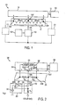
FIG. 1 illustrates asystem 100 having aresistive structure 101, consistent with an embodiment of the present invention. In one embodiment, theresistive structure 101 has a total resistance Rx between afirst node 130A and asecond node 130B. At least one additional node (e.g.,third node 130C) is provided that electrically and/or mechanically is located between thefirst node 130A and thesecond node 130B. For example, a first partial resistance Rx1 appears between thefirst node 130A and thethird node 130C and a second partial resistance Rx2 appears between thethird node 130C and thesecond node 130B. A total resistance Rx is provided by the sum of partial resistances Rx1 and Rx2. The magnitude of the resistances Rx, Rx1, and Rx2 may be unknown. - The
resistive structure 101 may be part of a circuit. In one embodiment, thefirst node 130A is connected to apower supply 110, and thesecond node 130B is connected to aload 111. For example, theresistive structure 101 acts as a current sense ("shunt") resistor, that facilitates the measurement of a current flowing throughresistive structure 101 by measuring the voltage across thefirst node 130A and thesecond node 130B and calculating the load current by Ohm's law, as provided by Equation 1 below.
- In one embodiment, a calibration
current circuit block 102 provides current (e.g., in the form of pulses) to resistive structure 101 (Rx). Accordingly, calibration currentgenerating circuit block 102 is used to measure the resistance of resistive structure 101 (Rx). In one example, the calibrationcurrent generating circuit 102 is coupled to at least thethird node 130C in at least one state of operation. "Coupled" in this context means that the calibration current need not be injected exactly into the third node; rather, any appropriate location in the vicinity of the third node may also be used to inject the calibration current. However, the closer to the third node the better the accuracy. A distinctive advantage provided by injecting a calibration current (ICAL) to thethird node 130C of theresistive structure 101 is that reactive components (e.g., such as power supply decoupling capacitors) tied tonodes 130A and/or 130B (e.g., 110 and 111) do not impair or disturb the calibration current pulses (ICAL). -
System 100 may include acontrol circuit 103 coupled to the calibration currentgenerating circuit block 102.Control circuit 103 has at least two states of operation to change a calibration current (ICAL) or to guide the calibration current ICAL to either one of at least two of the three nodes of the resistive structure (i.e., 130A, 130B, and 130C) alternately. For example, instead of changing the calibration current (ICAL) between two states, (which may be "calibration current ON" and "calibration current OFF," two different magnitudes of the calibration current, or two different signs of the calibration current), the calibration current may be "ON" during the calibration but alternated betweennode 130C andnode 130A, or be alternated betweennode 130C andnode 130B. For example, the alternation may be accomplished by electronic switching means, such as a pair of MOSFETs (not shown inFIG.1 ) tied between the output of the calibrationcurrent source 102 andnode 130C andnodes 130A/B of theresistive structure 101, respectively. It will be understood that adding such MOSFETs (or any other circuit elements) to the calibration current path still couples the calibration current generating circuit to thethird node 130C of theresistive structure 101. -
System 100 may include a signalconditioning circuit block 104 that is coupled to thefirst node 130A, thesecond node 130B, and thethird node 130C to form a conditioned signal at itsoutput 105. The signal at theoutput 105 provides the difference (or an amplified difference) between the electrical potential at the third node (130C) of theresistive structure 101 and the weighted average of the electrical potential at the first and second nodes (130A, 130B) of theresistive structure 101. - In one embodiment,
system 100 includes a signalprocessing circuit block 106 that is coupled to theoutput 105 of theconditioning circuit block 104. The signalprocessing circuit block 106 uses the signal at the output 105 (provided by the conditioning circuit block 104) to determine the resistance Rx of theresistive structure 101. Thesignal processing block 106 is discussed in more detail later. -
FIG. 2 is a more detailed representation of asystem 200 having aresistive structure 201, consistent with an embodiment of the present invention. For example, theresistive structure 201 may be a piece of resistive material having at least afirst connection node 230A, asecond connection node 230B, and athird connection node 230C.Connection node 230C is betweennode 230A andnode 230B. In one embodiment,connection node 230C is halfway betweenconnection nodes 
- Accordingly, the desired response signal at
node 230C is maximized, which decreases in amplitude thefurther node 230C is moved away from the center of theresistive structure 201. In one embodiment,node 230C (from which the signal is taken) is positioned away from the center (e.g., at a distance where the resistance is 1/3 of the total resistance). It should be noted that whennode 230C is too close to one of thenodes - The calibration current
generating circuit block 202 may comprise a regulation transistor M1. In one embodiment, the regulation transistor M1 is a double-diffused metal-oxide-semiconductor (DMOS) transistor. The drain of the regulation transistor M1 may be tied to thethird connection node 230C. In one embodiment, the drain of regulation transistor M1 is coupled to thethird connection node 230C by tying the drain to one or more locations in the vicinity of the third node of the resistive structure. In one embodiment, the calibration currentgenerating circuit block 202 includes a reference resistor Rs having a first node coupled to the source of the regulation transistor M1 and a second node coupled to Vss (or ground). Reference resistor Rs generally does not see the load current ILOAD; rather, it sees the calibration current ICAL, which may be orders of magnitude smaller than the maximum load current. Further, the calibration current ICAL may comprise short pulses and have a small duty cycle. Accordingly, resistor Rs may be much smaller in size and of lower power rating (and hence, of lower cost) than a precision shunt resistor that is able to sustain the full load current. If an optional secondary calibration step (described later) is added, reference resistor Rs may also have a large tolerance, large temperature coefficient, and poor stability (and thus be of even lower cost), without substantially impairing the precision of theresistance calibration system 200 discussed herein. -
Control circuit block 203 may comprise an op-amp 240 and a programmable referencevoltage source V REF 242 coupled to the (e.g., DMOS) regulation transistor M1 and reference resistor Rs to form a current servo loop. For example,control circuit block 203 provides a calibration current as provided inEquation 3 below:
- In one embodiment, at least two states of the control means are implemented by providing two states of the programmable reference
voltage source V REF 242. For example, in a first state, zero voltage is provided and in a second state, a positive voltage is provided. The positive voltage may be approximately 1 V. In some embodiments, thereference voltage V REF 242 need not be too precise and it also may have a large temperature drift without substantially impairing the precision of theresistance calibration system 200 discussed herein, as long as the reference voltage is substantially stable for the brief periods of time during which the calibration current is switched "ON." For example, thereference voltage V REF 242 defines the gross magnitude of the calibration current pulse during a brief interval of time. If the reference voltage is off by some 10% to 30% from the designed typical value, thecalibration 200 discussed herein still may work precisely as long as the circuitry does not exceed its operational margins and if the reference voltage is also used within the signal processing, which is described later. - In one embodiment, the signal
conditioning circuit block 204 comprises an interpolator (IP) 220 that forms a weighted average voltage between the voltages atnode 230A (Va) and atnode 230B (Vb) as provided by Equation 4a below.
- Accordingly, Equation 4a describes a proportional relationship. For example, when passive interpolators (e.g., based on resistors and/or capacitors) are used the proportionality factor typically is 0.5 and Equation 4a takes the form of Equation 4b below:

- In another example, where active interpolators (e.g., based on operational amplifiers) are used, there may be an interpolator gain GI. In this regard, the proportionality factor may be other than 0.5, as provided by Equation 4c below:

- In Equations 4a to 4c above, "a" is an interpolation parameter that may be constant or variable. It corresponds to the location of the
third node 230C in relation to the first andsecond nodes resistive structure 201. In some embodiments, numerical values for the interpolation parameter "a" may exceed this range. However, exceeding this range may reduce attainable accuracy of the calibration. For example, accuracy of the calibration for a given calibration current level is best when the signal Vavg has the largest amplitude, which occurs when interpolation parameter "a" is zero or close to zero. High accuracy can be accomplished by reducing the mechanical, thermal and electrical tolerances of the resistive structure to a reasonable level and by bringing thethird node 230C as close to the electrical center equipotential line between the first and second nodes as reasonably possible (e.g., by proper exploitation of the given capabilities of the manufacturing process used to make the resistive structure). For basic geometries, such as a resistive structure having a rectangular shape, the preferred location to place thethird node 230C (e.g., such that the interpolation parameter "a" is close to zero) is at the centroid of the shape betweennodes - Signal
conditioning circuit block 204 also may include a difference amplifier (AMP) 222 that is configured to amplify the difference between a voltage Vc at thethird node 230C and the weighted average voltage Vavg provided byinterpolator 220 with a gain factor of GA, as provided by Equation 5a below.
- If an active interpolator having an interpolator gain GI is used, then the input of the
difference amplifier 222 coupled to thethird node 230C of theresistive structure 201 has a gain as provided by Equation 5b below.
- In one embodiment, this difference amplifier gain function of Equation 5a and the weighted average function of the
interpolator 222 may be combined by configuring an operational amplifier according to known procedures to achieve a transfer function as provided by Equation 6 below.
- For example, the calculation above involves a first input network coupling Va and Vb to a first input of an operational amplifier and a second input network coupling Vc to a second input of the operational amplifier. Further, a feedback network couples the output of the operational amplifier to the inverting input of the operational amplifier. The first and second input network and the feedback network may be resistive or capacitive.
- In one embodiment, the
interpolator 220 comprises a string of resistors having a center tap (or multiple selectable taps arranged around the center). The tap location (e.g., corresponding to interpolation parameter "a") is chosen to correspond to the location of thethird node 230C in relation to the first andsecond nodes - In one embodiment, the
interpolator 222 may be combined with the amplifier 240 (e.g., configured as a switched capacitor circuit), where the interpolation parameter "a" is implemented as a ratio of input capacitors of the switched capacitor circuit, or is inherent in the switching sequence. An advantage of such a capacitive interpolator is that it does not draw DC currents from the resistive structure, so it may offer the same or better calibration accuracy as a high ohmic resistive interpolator does. - In various embodiments where a distributed
resistive structure 201 is used (e.g., such as a PCB foil run), more than one node (e.g., C, C', C" ofFIG. 8 ) near or at the center of theresistive structure 201 may be used to inject calibration currents. Further, more than one of these nodes may be used to provide a voltage Vc to an input node of thedifference amplifier 222. In one embodiment, if more than one such node contributes to the voltage level at node Vc, thedifference amplifier 222 may include multiple inputs to accommodate the multiple input voltages. For example, each voltage input to theamplifier 222 may have equal or individual gain factors. In one embodiment, finite element analysis of the distributedresistive structure 201 is used to determine optimum gain factors for each input of a multiple input difference amplifier. In the finite element model, the gain factors are easily determined from the relative magnitude of the electric potentials at the nodes providing the multiple input voltages when a known calibration current is injected at one or multiple other nodes in their vicinity. - The signal
processing circuit block 206 may comprise a switched capacitor integrator and comparator (e.g., an analog to digital converter (ADC) based on delta-sigma modulator techniques). For example, the switched capacitor integrator and comparator are configured as a modulator of a delta sigma analog-to-digital converter. The modulator uses a reference voltage that tracks thereference voltage 242 that is used to regulate the calibration current ICAL. In one embodiment, the signalprocessing circuit block 206 adds or subtracts Vout and/or reference voltages from a stored integration result and checks for the sign of the integration result. A digital decimation filter may be added in hardware or implemented in software. In one embodiment, the reference voltage for the ADC is the same as thereference voltage 242 for thecontrol circuit block 203. Put differently, the reference voltage for the ADC andreference voltage 242 both are derived from a common voltage source. In this case, the ADC result automatically corrects for any imprecision or temperature drift of the reference voltage source, as mentioned above. - With the foregoing overview of the
system 200, it may be helpful now to consider a high-level discussion of an exemplary operation of thesystem 200. In a first phase of operation, referencevoltage source V REF 242 is set to zero (i.e., calibration current Ical is OFF) and Vout atnode 205 is sampled (e.g., by a delta sigma ADC within the signal processing block 206). This may be the first sample of a correlated double sampling (CDS) signal processing method. - In a second phase of operation, reference
voltage source V REF 242 is set to a positive voltage (e.g., to 1.23V, which may be provided by a band-gap reference, but also can be from a reference that is much less precise than a band-gap reference). The calibration current drawn from thethird node 230C is provided by Equation 7 below.
- After a brief delay (i.e., when the calibration current is sufficiently stable), Vout at
node 205 is sampled again. In one embodiment, this represents the second sample of the CDS signal processing method. It should be noted that other sampling, measurement, or digitizing approaches known in the art of signal processing may be used, as long as they achieve the capture of the Vout difference between the two phases of operation. In one embodiment, the first phase and second phase operations are periodic. - In one embodiment, an idle phase is included. For example, in the optional idle phase, reference
voltage source V REF 242 is again set to zero volts. To save power during the optional idle phase, all the functional blocks discussed above (such as referencevoltage source V REF 242,AMP 222,Interpolator 220, and the ADC) may be set to a power down state. The optional idle phase also helps to cool down the electronic components that generated the calibration current pulse. As noted above, the idle phase is optional since the same cool down effect can be achieved in one embodiment by making the first phase of operation significantly longer than the second phase of operation. - For example, the absolute value of the difference between the signal samples taken in the first phase and the second phase is proportional to the product of the total resistance Rx * ICAL, even in the presence of offset voltages in the amplifiers or in the ADC. The proportionality factor itself may depend on the
total system 200 gain. An advantage of the exemplary signal processing technique discussed herein is that parasitic thermocouple voltages at the threenodes - In one embodiment, if the reference
voltage source V REF 242 is also used in the ADC, it is not included in the system gain equation for Rx / Rs. Accordingly, the referencevoltage source V REF 242 need not be very precise. - Further, in one embodiment, if the interpolation parameter "a" discussed above is chosen such that the weights used in forming the weighted average of the voltages are proportional to the magnitude of the partial resistances Rx1 and Rx2, then the load current flowing though the resistive structure 201 (Rx) also has no effect on the measurement of the resistive structure 201 (Rx).
- If the resistive structure is such that the interpolation parameter "a" does not need tuning (e.g., when there are no significant thermal gradients across the resistive structure or if its temperature coefficient of resistance is small), a trim circuit may be used to set the interpolation parameter "a" to an optimum value. For example, this optimum value may be determined once during the production of the system. For example, if the resistive structure is part of an integrated circuit, laser blown fuse links or some other known form of trimming circuitry may be used to choose one of several taps on a resistive interpolator to set the interpolation parameter "a" to an optimum value.
- In one embodiment, automatic tuning of the interpolation parameter "a" of the interpolation (performed by interpolator 220) can be accomplished by varying interpolation parameter "a" until Vout is minimal in the first phase of operation, (e.g., when calibration current is zero).
- Tuning circuitry for automatic tuning of the interpolation parameter "a" may take several forms. In a preferred embodiment, tuning is based on detecting a residual signal Vout (205) that is caused by a change in the magnitude of currents that enter the
resistive structure 201 through the first node and exit at the second node (or vice versa), during operation of the system. - For example, the tuning circuitry or tuning method discussed herein may use the correlation between load current (e.g., observed as voltage Vab between
nodes node 205. The ideal tuning point is where the correlation is minimized. In one example, to achieve minimization of the correlation, the correlation circuit simply provides the sign of the correlation, and the tuning process changes the chosen tap on a resistive interpolator up or down, depending on the sign. After a brief period of operation, the tuning process jumps between the two most optimum taps. Interpolation parameter "a," which enters the gain equation for the calibration process as a factor (1-a2), follows from the chosen tap location according to Equation 5 above. This factor (e.g., close to 1.00 for small deviations from the ideal center tap case), may be ignored for systems calling for modest accuracy. However, in more accurate systems this factor may also be used by the signal processing block to correct for a change in calibration gain. Hence, the system can automatically track and correct for any deviations from the ideal center tap case. -
FIG. 9 illustrates acorrelation circuit 900, compatible with an embodiment of the present invention. In the example ofFIG. 9 ,correlation circuit 900 comprises an analog fourquadrant multiplier 950 coupled to anintegrator 970. The differential voltage Vab across the input nodes of theamplifier 940 provides the first input signal and Vout provides the second input signal of the fourquadrant multiplier 950. In one embodiment, differential voltage Vab is amplified by anamplifier 940 before providing it to the fourquadrant multiplier 950. In one embodiment, a delta sigma modulator of an ADC is used in lieu of ananalog integrator 970. To allow reuse of an integrator or ADC used in the calibration circuitry for the tuning process, aswitch 960 may be used. For example, theswitch 960 couples theintegrator 970 to Vout in a "CAL" state while coupling theintegrator 970 to the multiplier (950) in a "TUNE" state to provide a correlator. If the load current is unidirectional, a two quadrant multiplier may be used instead. The correlation also may be performed in the digital domain by correlating the PWM bit streams of two delta sigma modulators, one being provided the signal Vab, and the other one being provided by Vout atnode 205. The signals Vab and/or Vout may be amplified before being sent to the multiplier. - In various embodiments, the correlation operation (i.e., the interpolation parameter "a" tuning process) may use the natural load current ripple caused by the inductor current ripple inherent to switch-mode power supplies, load current ripple that may be caused by changing the data processing (CPU) load, and the like. For example, current ripple of sufficient amplitude may not be available to perform the
interpolator 220 tuning. In this regard, system software may provoke sufficient load current ripple by, for example, performing many computations from time to time, and less computations at other times, to modulate the load current. The system software also may intelligently control the tuning process to occur during such phases of operation where sufficient load current is present due to a varying computational load. - Load current ripple suitable for the correlation operation may also be generated by modulating the voltage feedback network of a switching or linear regulator power supply. For example, such load current ripple can be achieved by coupling a rectangular digital modulation signal to the feedback pin of a switching power supply via a resistor. For example, the resistance of the resistor is chosen such that a digital signal swing changes the output voltage of the switching power supply within the limits specified by the load. For example, for a load that can tolerate a 10% supply voltage variation, the modulation of the output voltage of the switching power supply can be set to 5%. In one embodiment, the period of the rectangular digital modulation signal is preferably is 10 to 100 times longer than the switching frequency. However, any other timing also may be used as long as the voltage control loop transient response to the modulation is detectable. For example, in the correlation operation, the voltage Vout of
node 205 may be multiplied with a signal derived from the digital modulation signal. In one embodiment, a delayed version of the modulation signal is used, where the delay is chosen such that optimum sensitivity of the correlation process is achieved. Instead of using the modulation signal, the voltage Vout ofnode 205 may be also be multiplied by the voltage difference between the voltage at thefirst node 230A and thesecond node 230B (Vab) or an amplified version thereof in the correlation operation. - In one embodiment, the
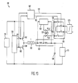
analog multiplier 950 is not used. Instead, the correlation operation uses the gate drive (switch pin) signal of a switching power supply. Reference now is made toFIG. 10 , which illustrates a system having a tunable interpolator and a correlator circuit that is based on polarity reversing switches which are driven by switching phases of a switch-mode power supply, consistent with an embodiment of the present invention. The gate drive output(s) 1081, 1082 of a switchingpower supply controller 1080 may be amplified, shaped to a digital control signal, extended, or reduced in time duration, by a switchgate conditioning circuit 1090. The resultingdigital control signals switch arrangement 1095. For example, the switch arrangement couples thevoltage Vout 1005 or itspolarity inverse 1006 from adifference amplifier 1022 to anintegrator 1070 or analog to digital converter (ADC) (e.g., a delta sigma ADC). As shown inFIG. 10 , the difference amplifier 1022 (e.g., corresponding todifference amplifier 222 ofFIG. 2 ) may have a differential output, thereby allowing changing the polarity of the signals atnodes integrator 1070. Alternatively, in case of single ended difference amplifier, a polarity changing switch arrangement under control of thedigital control signals difference amplifier 1022. However, additional gating for the desired timing window should then be added to its output. For example, thetunable interpolator 1020 corresponds to 220 inFIG. 2 , and theresistive structure 1001 corresponds to 201 inFIG. 2 . In one embodiment, the switchingpower supply 1000 includes aPFET 1083, anNFET 1084, aninductor 1085, and acapacitor 1086. The load 1111 is coupled to the output of theresistive structure 1001. - In one embodiment, where a switching power supply is not present or an existing regulator cannot be used for the correlation processes as described above, the sufficient load current ripple is provided by a tuning current source coupled to at least one of the
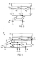
nodes FIG. 3 , a calibration current source may be reused as a tuning current source for a load current ripple by providing additional paths to couple the ripple current tonode nodes node 330C. For example some DMOS transistors (e.g., M2, M3, M4) may be added in the output branch of the calibration current generating circuit (e.g., 202 inFIG. 2 ). Transistor M3 is switched ON and M2/M4 are switched OFF to inject a calibration current pulse into thethird node 330C. To generate a tuning current pulse, M3 is switched OFF and either M2 or M4 are switched ON. In one embodiment, transistor M4 is omitted if ping-pong operation betweennodes nodes -
FIG. 4 illustrates asystem 400 that is capable of steering current in a resistive structure, consistent with an embodiment of the present invention.FIG. 4 illustrates a simplified configuration to more easily describe certain aspects of the invention. In one embodiment, several DMOS transistors (e.g., M1B and M1C) steer the calibration current pulses ICAL alternately tonodes switches operational amplifier 440 can be directed to eithernode 430C ornode 430B, depending on which switch is closed. In one example, these pulses directed tonode 430B of theresistive structure 401 may be used in lieu of natural load current ripple to tune the interpolation that is provided by the interpolator (within signal conditioning block 404). Alternatively, the drain of regulation transistor M1 B may be tied tonode 430A. In one embodiment, the drain of regulation transistor M1 B is tied to thenode - In various embodiments, the calibration current source may also be implemented by splitting a switch or pass transistor of a switch-mode or linear power supply. In this regard,
FIG. 5 illustrates asystem 500 that steers current in a resistive structure by splitting a switch, consistent with an embodiment of the present invention. For example, part of the load current ILOAD is periodically diverted from a first node (e.g., 530A) of theresistive structure 501 into a third node (e.g., 530C). This may be particularly beneficial if theresistive structure 501 and the switch or pass transistors (e.g., 5M2 and 5M1) are integrated on a switch-mode or linear-mode power supply chip. In one embodiment, the top metal layers of a semiconductor chip or bond wires may be used as theresistive structure 501. - It may be helpful now to consider a high-level description of an exemplary operation of the
system 500. In one embodiment, in the first phase of operation, transistor 5M1 is OFF while transistor 5M2 carries all of the load current ILOAD. In the second phase of operation, 5M1 is turned ON thereby carrying part of the load current ILOAD. For example, at this stage, a part of ILOAD serves as the calibration current ICAL for theresistive structure 501. In one embodiment, the voltage drop across resistor 557 (Rs) is used to determine the calibration current ICAL or to regulate it to a desired value by including transistor 5M1 in the feedback loop. Since calibration current ICAL may be orders of magnitude less than the maximum load current ILOAD, both transistors 5M1 andresistor 557 may be configured to handle a much smaller current than transistor 5M2 andresistive structure 501. Accordingly, in this embodiment, the calibration current pulses do not contribute to the power consumption. - The foregoing embodiments can be augmented with an additional (e.g., secondary) calibration step, where the resistor 557 (Rs) of the calibration current branch ICAL is calibrated against an additional reference resistor or a reference current, as represented the secondary calibration
current source 507 ofFIG. 5 . In one embodiment, secondary calibrationcurrent source 507 comprises a switchable (e.g., 569) referencecurrent source 572. Whenswitch 569 is ON, the referencecurrent source 572 is coupled to resistor 557 (Rs) of the calibration current circuit block. For example, switch 569 is switched ON when the primary calibration system (for the resistive structure 501) is idle and does not produce a calibration current ICAL. During this phase of operation, the transistors 5M1 (or M1C and M1B ofFIG. 4 ) are switched OFF, such that a secondary calibration current IREF flows through series resistor 557 (or reference resistor Rs ofFIG. 4 ) undisturbed. - The magnitude of resistor 557 (Rs) is based on the circuit that measures the resistance, such as an ADC that measures the voltage across resistor 557 (not shown). For example, this secondary calibration step may be useful for implementations where the resistor 557 (or any resistor, such as Rs) associated with the calibration current generating circuit is unstable, unknown, subject to process tolerances, or has high temperature coefficients. In the example of
FIG. 5 ,resistor 557 itself may be of the same metal layer asresistive structure 501. Accordingly,resistor 557 may have the same uncertainties - which are calibrated out in the secondary calibration step. However, sinceresistor 557 only needs to accommodate a small fraction of the maximum load current ILOAD, theresistor 557 can be made smaller in area and be higher ohmic thanresistive structure 501. The same reasoning may apply to any resistors in the switchable referencecurrent source 507 that generates the secondary calibration current Iref. - The reduction in size of the
resistor 557 may have additional benefits. For example, if the magnitude of Iref is small enough, more stable and precise resistors (such as Silicon-Chrome thin-film resistors) may be used in the switchable referencecurrent source 572 to stabilize Iref. Accordingly, including a secondary calibration capability (through reference block 507) may substantially relax the requirements for the material and construction ofresistor 557. Such secondary calibration capability may also be added to any calibration current defining resistors Rs as discussed above, by adding a secondary calibrationcurrent source 507 to Rs, and providing a circuit to measure the voltage across reference resistor Rs that is caused by the secondary calibration current. The circuit within secondary calibrationcurrent source 507 may be similar to the example seen inblock 202 ofFig. 2 . It will be understood that any other circuit, means, and method known in the art to generate precision reference currents may also be used based on the concepts discussed herein. - Adding the secondary calibration step as discussed above further reduces the current and power levels used to generate the final precision reference current Iref on which the calibration of Rx of the
resistive structure 101 is based in the end. This reduction of current and power levels can be several orders of magnitude per calibration step. This concept can be extended to a ternary (or higher) calibration step(s) until current and power levels are achieved for which a precision reference resistor can be provided at desired cost. The reference resistor also may be synthesized by a known technique that uses switched capacitor or charge balancing circuits that derive a reference current from a reference voltage source, a capacitor, and a time-base. - In some applications (e.g., where the typical broadband sinc spectrum of calibration current pulses is not desired), a resonant tank circuit may be used as a calibration current source. In this regard,
FIG. 6 illustrates part of asystem 600 that measures the resistance of a resistive structure 602, consistent with an embodiment of the present invention. The example ofsystem 600 includes a resonanttank circuit block 608 comprising an inductor 6L1 in series with a capacitor 6C1. In one embodiment, thetank circuit 608 is excited by inductive or capacitive coupling. For example, thetank circuit 608 is excited by anexcitation source 609 via capacitive coupling with capacitor 6C2. In one embodiment, thetank circuit 608 generates a pure sinusoidal calibration current of a predetermined frequency with no harmonics. In one embodiment, thetank circuit 608 is configured to a frequency band where it does not interfere with any sensitive signals in the system. -
FIG. 7 illustrates an exemplaryresistive structure 701, consistent with an embodiment of the present invention. For example, the resistive structure may be a distributed resistance provided by a printed circuit board (PCB)foil run 701.FIG. 7 shows an exemplaryresistive structure 701 in which theelectrical node 130C fromFIG. 1 is essentially split into twonodes resistive structure 701. The calibration current Ical is still injected atnode 730C, but the signalconditioning circuit block 704 is now connected tonode 730C'. This configuration yields a pseudo-Kelvin connection where the influence of the parasitic resistances in the Ical path are mitigated by splitting the third node into two nodes (e.g., 730C and 730C').FIG. 7 illustrates the approximateequipotential lines 770 caused by Ical. It should be noted that when the calibration current Ical is flowing, the voltages atnodes nodes node 730A tonode 730B, there is a linear relationship (or an additional gain factor to be accounted for) in theresistive structure 701 calibration process, which can be derived for a given geometry. For example, the linear relationship or the gain factor can be determined by direct measurement of a prototype or by finite element analysis software. -
FIG. 8 illustrates another variation of the pseudo Kelvin connect approach, consistent with an embodiment of the present invention. For example, there is a two layer PCB board, having a bottom layer (striped) and a top layer (not striped). The drain of the transistor 8M1 is coupled to the bottom layer of the PCB foil runs. Preferably, the bottom layer PCB foil runs are of equal length and as symmetrical as possible, through via holes tophysical nodes 830C' and 830C", where both receive part of the calibration current. Similarly, in one embodiment,nodes conditioning circuit block 804. In yet another embodiment that is able to handle very large currents, theresistive structure 801 may be a part of a plane within a multilayer PCB and thenodes -
FIG. 11 illustrates an exemplary resistive structure following another pseudo Kelvin connect circuit, consistent with an embodiment of the present invention. For example, the calibration current Ical from regulation transistor 11M1 is injected at anode 1130C of the resistive structure, which may be a printed circuit board trace or plane. The third node response signal is formed by averaging the voltages fromadjacent nodes 1130C' and 1130C". In one example, the averaging is performed by two equally sized resistors orcapacitors nodes 1130C' and 1130C", respectively. The common node 1104C of the resistors or capacitors used as coupling elements electrically corresponds to the third node (130C) of the idealized equivalent resistive structure comprising lumped elements as provided in the discussion ofFIG. 1 . It should be noted that other variations of how the calibration current generation circuit and thesignal conditioning circuit 1104 may be coupled to a third node of an resistive structure by means of additional electronic components are possible without deviating from the scope and spirit of the embodiments discussed herein. - The components, steps, features, objects, benefits and advantages that have been discussed herein are merely illustrative. None of them, nor the discussions relating to them, are intended to limit the scope of protection in any way. Numerous other embodiments are also contemplated. These include embodiments that have fewer, additional, and/or different components, steps, features, objects, benefits and advantages. These also include embodiments in which the components and/or steps are arranged and/or ordered differently. For example, bipolar transistors (e.g., PNP or NPN) can be used instead of MOS transistors. A PNP may be used instead of NPN, and a PMOS may be used instead of NMOS. Accordingly, it is intended that the invention be limited only in terms of the appended claims.
Claims (24)
- A system for measuring electrical resistance, comprising:a resistive structure having:a first node at a first end of the resistive structure;a second node at a second end of the resistive structure; anda third node on the resistive structure between the first and second nodes;a calibration current generation circuit having an output coupled to the third node of the resistive structure; anda signal conditioning circuit comprising:a first input coupled to the first node of the resistive structure;a second input coupled to the second node of the resistive structure;a third input coupled to the third node of the resistive structure; andan output,wherein the signal conditioning circuit is configured to provide at its output a signal proportional to a difference between a voltage at the third node and a weighted average of the voltages at the first and second nodes of the resistive structure.
- The system of claim 1, further comprising a signal processing circuit coupled to the output of the signal conditioning circuit, wherein the signal processing circuit is configured to calculate the resistance of the resistive structure.
- The system of claim 1 or 2, wherein the calibration current generation circuit is configured to sequentially couple at least two different calibration currents of different magnitude or sign into the third node of the resistive structure, and the signal processing circuit is configured to calculate the resistance of the resistive structure from a difference between a first output voltage of the signal conditioning circuit when the calibration current is set to a first value, and a second output voltage of the signal conditioning circuit when the calibration current is set to a second value.
- The system of claim 3, wherein the calibration current generation circuit comprises a current servo loop having a regulation transistor that is configured to regulate the calibration current to a value determined by a reference voltage and a reference resistor (Rs).
- The system of claim 4, wherein the regulation transistor of the current servo loop is configured to be switched between at least two current values; and/or
wherein the regulation transistor of the current servo loop is configured to be switched ON and OFF. - The system of claim 4 or 5, wherein the signal processing circuit comprises a switched capacitor integrator and a comparator,
wherein:the switched capacitor integrator and comparator may be configured as a modulator of a delta sigma analog-to-digital converter; andthe modulator may be configured to use a reference voltage that tracks the reference voltage that is used to regulate the calibration current. - The system of any one of claims 1 to 6, wherein the signal conditioning circuit comprises:an interpolator having a first input coupled to the first node of the resistive structure, a second input coupled to the second node of the resistive structure, and an output; anda difference amplifier having a first input coupled to the output of the interpolator and a second input coupled to the third node of the resistive structure, wherein the difference amplifier is configured to amplify a difference between the third node of the resistive structure and a voltage at the output of the interpolator.
- The system of claim 7, wherein the interpolator is configured to provide a voltage at its output based on:a voltage Va at the first node of the resistive structure;a voltage Vb at the second node of the resistive structure; andan interpolation parameter "a," wherein,the voltage at the output is equal or proportional to 0. 5*[(1-a)*Va + (1+a)*Vb].
- The system of claim 8, further comprising a circuit for trimming the interpolation parameter "a" such that the voltage at the output of the interpolator is substantially the same magnitude as the voltage at the third node of the resistive structure when the calibration current is zero,
the system optionally further comprising a circuit configured to tune the interpolation parameter "a" such that influence of load current flowing though the resistive structure on the signal at the output of the signal conditioning circuit is minimized. - The system of claim 8 or 9, further comprising a correlator circuit having a first correlator input coupled to the output of the signal conditioning circuit,
wherein the correlator circuit may comprise a multiplier coupled to an integrator. - The system of claim 10, wherein:the output of the signal conditioning circuit is a differential output having positive and negative polarity output nodes; andthe correlator circuit comprises a polarity interchanging switch arrangement coupled to an integrator,wherein the correlator circuit may further include a second input, wherein the second input may be:differential; andcoupled to the first and second nodes of the resistive structure.
- The system of claim 10 or 11, further comprising at least one tuning current source coupled to at least the first or second node of the resistive structure, wherein the at least one tuning current source is configured to provide tuning current pulses for tuning the interpolator.
- The system of claim 12, wherein the calibration current generation circuit comprises a servo loop having:a regulation transistor configured to regulate the calibration current to a value determined by a reference voltage and a reference resistor;a first current steering transistor coupled between the regulation transistor and the third node of the resistive structure; anda second current steering transistor coupled between the regulation transistor and one of (i) the first node or (ii) the second node of the resistive structure.
- The system of claim 12 or 13, further comprising a plurality of switches having a common node coupled to a reference voltage and configured to render active one of (i) the first regulation transistor or (ii) the second regulation transistor, wherein:the calibration current generation circuit comprises a servo loop having at least two regulation transistors configured to regulate the calibration or tuning current to a value determined by a reference voltage and a reference resistor (Rs);the first regulation transistor is coupled to the third node of the resistive structure; andthe second regulation transistor is coupled to one of the (i) first or (ii) second node of the resistive structure.
- The system of any one of claims 7 to 14, further comprising:an input voltage node (Vin);a reference resistor;at least two current steering transistors, wherein a first current steering transistor has a source coupled to the third node of the resistive structure and a second current steering transistor has a source coupled to the first node of the resistive structure;a control circuit having a separate output coupled to a gate of the at least two current steering transistors, respectively;wherein:the first node of the reference resistor is coupled to the input voltage node;the second node of the reference resistor is coupled to the third node of the resistive structure via the first current steering transistor;the input node is coupled to the first node of the resistive structure via the second current steering transistor; andthe control circuit is configured to independently switch the current steering transistors ON and OFF; andwherein the system may further comprise a secondary calibration current source coupled to the reference resistor.
- The system of any one of claims 7 to 15, wherein the calibration current generation circuit comprises a resonant tank circuit that is coupled between the third node of the resistive structure and to either the first or second node of the resistive structure.
- A method of measuring resistance of a resistive structure having a first node at a first end of the resistive structure, a second node at a second end of the resistive structure, and a third node between the first node and the second node of the resistive structure and adapted to receive a calibration current; a signal conditioning circuit comprising a first input coupled to the first node of the resistive structure, a second input coupled to the second node of the resistive structure, a third input coupled to the third node of the resistive structure; and an output, the method comprising:determining a first calibration signal by measuring a voltage at the output when no calibration current is injected into the third node of the resistive structure;injecting a calibration current into the third node of the resistive structure;determining a second calibration signal by:interpolating voltages at the first and second nodes of the resistive structure; andsubtracting the interpolated voltage from a voltage at the third node of the resistive structure; anddetermining an absolute value of a difference between the determined first calibration signal and the determined second calibration signal, wherein the absolute value is proportional to a product of the resistance of the resistive structure and the calibration current.
- The method of claim 17, wherein the calibration current is injected into the third node of the resistive structure in a form of a pulse; and/or wherein the method further comprises performing the first calibration signal and the second calibration signal periodically; and/or
wherein the method further comprises measuring a current flowing between the first node and the second node of the resistive structure. - The method of claim 17 or 18, wherein interpolating the voltage at the first node of the resistive structure and the voltage at the second node of the resistive structure includes determining a weighted average voltage (Vavg) between the voltages at the
first node of the resistive structure and at the second node of the resistive structure based on:a voltage Va at the first node of the resistive structure;a voltage Vb at the second node of the resistive structure; andan interpolation parameter "a," wherein,
- The method of claim 19, further comprising:amplifying a difference between the weighted average voltage (Vavg) and a voltage at the third node of the resistive structure by a factor GA; andproviding the amplified difference as an output voltage at the output (Vout),wherein the output voltage at the output (Vout) may be based on:a voltage Vc at the third node of the resistive structure, wherein,

- The method of claim 19 or 20, further comprising tuning the signal conditioning circuit to compensate for a difference between a resistance between the first and third nodes of the resistive structure and a resistance between the second and third nodes of the resistive structure.
- The method of claim 21, wherein the tuning comprises varying the interpolation parameter "a" until the voltage at the output is minimized when no calibration current is injected into the third node of the resistive structure.
- The method of claim 22, wherein the tuning further comprises using a load current ripple as a signal source, wherein the load current ripple is caused by at least one of:(i) a switch-mode power supply coupled to the first or third node of the resistive structure; or(ii) a load coupled to the first or third node of the resistive structure; andwherein the switch mode power supply may be modulated during the tuning process to generate a load current ripple.
- The method of claim 22 or 23, wherein the tuning further comprises providing a current pulse to at least one of (i) the first node of the resistive structure or (ii) the second node of the resistive structure to create an artificial ripple current in the resistive structure to tune the signal conditioning circuit.
Applications Claiming Priority (1)
| Application Number | Priority Date | Filing Date | Title |
|---|---|---|---|
| US13/734,581 US8947101B2 (en) | 2013-01-04 | 2013-01-04 | Method and system for measuring the resistance of a resistive structure |
Publications (2)
| Publication Number | Publication Date |
|---|---|
| EP2752672A1 true EP2752672A1 (en) | 2014-07-09 |
| EP2752672B1 EP2752672B1 (en) | 2019-11-13 |
Family
ID=49949479
Family Applications (1)
| Application Number | Title | Priority Date | Filing Date |
|---|---|---|---|
| EP14000004.3A Active EP2752672B1 (en) | 2013-01-04 | 2014-01-02 | Method and system for measuring the resistance of a resistive structure |
Country Status (4)
| Country | Link |
|---|---|
| US (1) | US8947101B2 (en) |
| EP (1) | EP2752672B1 (en) |
| CN (1) | CN103913639B (en) |
| TW (1) | TWI503646B (en) |
Cited By (3)
| Publication number | Priority date | Publication date | Assignee | Title |
|---|---|---|---|---|
| EP3159704A1 (en) * | 2015-10-23 | 2017-04-26 | ALSTOM Transport Technologies | Measuring chain for a signalling electronic circuit |
| CN108427017A (en) * | 2018-01-31 | 2018-08-21 | 上海思愚智能科技有限公司 | A kind of test system and terminal |
| WO2018158330A1 (en) * | 2017-03-03 | 2018-09-07 | Continental Automotive Gmbh | Current sensor with optimised current density distribution, and method for determining a load current |
Families Citing this family (21)
| Publication number | Priority date | Publication date | Assignee | Title |
|---|---|---|---|---|
| WO2014162952A1 (en) * | 2013-04-02 | 2014-10-09 | 株式会社村田製作所 | Dummy load circuit and charge detection circuit |
| EP3015877B1 (en) * | 2014-10-31 | 2016-10-26 | Samsung SDI Co., Ltd. | Method for calibrating a current measuring device |
| DE102015216712A1 (en) * | 2015-09-01 | 2017-03-02 | Continental Automotive Gmbh | Device for detecting a resistance value of a measuring resistor of a measuring sensor |
| DE102016202501B4 (en) * | 2016-02-18 | 2022-03-17 | Continental Automotive Gmbh | Method for determining a calibration current pulse |
| DE102016206958A1 (en) | 2016-04-25 | 2017-10-26 | Continental Automotive Gmbh | Method for determining a load current and battery sensor |
| US10709616B2 (en) * | 2016-05-10 | 2020-07-14 | Xtrava Inc. | Contactless magnetic probe sensing and impedance imaging of liquid and solid excrement in diapers and other underclothing |
| CN106199426B (en) * | 2016-07-01 | 2019-06-21 | 贵阳华旭科技开发有限公司 | Direct current generator ripple fictitious load |
| EP3546956B1 (en) * | 2018-03-29 | 2020-10-14 | AMS Sensors UK Limited | Circuit for measuring a resistance |
| CN109270429B (en) * | 2018-08-31 | 2021-02-05 | 中国船舶重工集团公司第七0九研究所 | Method for measuring noise of multi-channel high-low temperature interface circuit board |
| CN109596871A (en) * | 2018-11-12 | 2019-04-09 | 中国计量科学研究院 | Quantum resistance standard device |
| CN109752597B (en) * | 2019-01-11 | 2021-07-02 | 北京东方计量测试研究所 | Inductance lead compensation device and method |
| US11391805B2 (en) | 2019-05-10 | 2022-07-19 | Hamilton Sundstrand Corporation | Systems and methods for current sense resistor built-in-test |
| WO2021262457A2 (en) | 2020-06-12 | 2021-12-30 | Analog Devices International Unlimited Company | Self-calibrating polymer nano composite (pnc) sensing element |
| DE112021005751T5 (en) | 2020-10-27 | 2023-08-17 | Analog Devices, Inc. | WIRELESS INTEGRITY ACQUISITION PROCUREMENT MODULE |
| KR102478075B1 (en) * | 2021-03-04 | 2022-12-15 | 현대모비스 주식회사 | Apparatus for reducing temperature effects in stray inductance based switching current measurement |
| JP7491881B2 (en) * | 2021-08-17 | 2024-05-28 | 株式会社デンソー | Current Sensors |
| JP7491879B2 (en) | 2021-08-17 | 2024-05-28 | 株式会社デンソー | Current Sensors |
| JP7491880B2 (en) | 2021-08-17 | 2024-05-28 | 株式会社デンソー | Current Sensors |
| CN115290945B (en) * | 2022-09-29 | 2022-12-23 | 山东阅芯电子科技有限公司 | High-precision test current source and method for power cycle test |
| CN115840181A (en) * | 2023-02-16 | 2023-03-24 | 南方电网产业投资集团有限责任公司 | Charging pile high-voltage sampling calibration circuit and method and electronic equipment |
| CN117949880B (en) * | 2024-03-21 | 2024-06-21 | 中国电子产品可靠性与环境试验研究所((工业和信息化部电子第五研究所)(中国赛宝实验室)) | Source meter direct-current micro-current indication four-quadrant calibration device and method |
Citations (11)
| Publication number | Priority date | Publication date | Assignee | Title |
|---|---|---|---|---|
| JPS60192270A (en) * | 1984-03-13 | 1985-09-30 | Fuji Electric Co Ltd | Multi-point resistance measuring device |
| US4591743A (en) | 1983-12-19 | 1986-05-27 | National Semiconductor Corporation | Temperature compensated current sensing circuit |
| JPS62168067A (en) * | 1986-01-21 | 1987-07-24 | Yamatake Honeywell Co Ltd | Measuring method for resistance value |
| US5804979A (en) * | 1997-05-13 | 1998-09-08 | Fluke Corporation | Circuit for measuring in-circuit resistance and current |
| US6469481B1 (en) | 1998-12-25 | 2002-10-22 | Kabushiki Kaisha Toyoda Jidoshokki Seisakusho | Parallel RC current detection circuit and DC/DC converter with a parallel RC current detection circuit |
| DE10133525A1 (en) * | 2001-07-11 | 2003-01-30 | Bosch Gmbh Robert | Pressure measurement sensor for motor vehicle control can be switched between measurement and test modes with aging and temperature effects same in two modes |
| EP1607753A1 (en) * | 2004-06-17 | 2005-12-21 | Micrel Incorporated | Current sense resistor circuit with averaging kelvin sense features |
| WO2006002446A1 (en) * | 2004-07-06 | 2006-01-12 | Lem Norma Gmbh | Method and device for uninterrupted current measurement |
| US7358710B2 (en) | 2006-04-18 | 2008-04-15 | Dell Products L.P. | Temperature-compensated inductor DCR dynamic current sensing |
| US7536577B2 (en) | 2005-01-11 | 2009-05-19 | International Business Machines Corporation | Calibration technique for power measurement and management over multiple time frames |
| DE102011078334A1 (en) * | 2011-06-29 | 2013-01-03 | Robert Bosch Gmbh | Method and system for calibrating a shunt resistor |
Family Cites Families (14)
| Publication number | Priority date | Publication date | Assignee | Title |
|---|---|---|---|---|
| US5121064A (en) * | 1990-08-31 | 1992-06-09 | Allied-Signal, Inc. | Method and apparatus for calibrating resistance bridge-type transducers |
| US6618684B1 (en) * | 2000-01-26 | 2003-09-09 | Elster Electricity, Llc | System and method for digitally compensating frequency and temperature induced errors in amplitude and phase shift in current sensing of electronic energy meters |
| EP1450167A1 (en) * | 2003-02-24 | 2004-08-25 | ELMOS Semiconductor AG | Method and device for measuring the resistance of an electronic component |
| US7042242B2 (en) * | 2004-05-25 | 2006-05-09 | Lsi Logic Corporation | Built-in self test technique for programmable impedance drivers for RapidChip and ASIC drivers |
| US7733163B1 (en) * | 2006-11-02 | 2010-06-08 | Marvell International Ltd. | Bias current compensation device and method |
| CN101021558B (en) * | 2007-03-23 | 2011-05-11 | 中国科学院光电技术研究所 | Method for measuring contact resistance of conductive ring by using three-ring method |
| KR100867536B1 (en) * | 2007-09-03 | 2008-11-06 | 삼성전기주식회사 | Received signal strength indicator capable of self-calibrating gain of limiter |
| US8106669B2 (en) * | 2007-09-27 | 2012-01-31 | Guildline Instruments Limited | High current precision resistance measurement system |
| US8779777B2 (en) * | 2010-06-04 | 2014-07-15 | Linear Technology Corporation | Dynamic compensation of aging drift in current sense resistor |
| TWI491889B (en) * | 2011-02-28 | 2015-07-11 | Hon Hai Prec Ind Co Ltd | Resistor-measuring circuit and electronic device using the same |
| CN102262184B (en) * | 2011-04-19 | 2013-02-27 | 哈尔滨工业大学 | Online storage battery internal resistance detector and internal resistance detection method |
| FR2975497B1 (en) * | 2011-05-16 | 2013-06-28 | Centre Nat Rech Scient | ELECTRONIC POWER CONVERTER |
| CN102818934A (en) * | 2011-06-08 | 2012-12-12 | 鸿富锦精密工业(深圳)有限公司 | Direct-current resistance measuring circuit for inductor |
| US8604777B2 (en) * | 2011-07-13 | 2013-12-10 | Allegro Microsystems, Llc | Current sensor with calibration for a current divider configuration |
-
2013
- 2013-01-04 US US13/734,581 patent/US8947101B2/en active Active
-
2014
- 2014-01-02 EP EP14000004.3A patent/EP2752672B1/en active Active
- 2014-01-03 TW TW103100261A patent/TWI503646B/en active
- 2014-01-06 CN CN201410005414.3A patent/CN103913639B/en active Active
Patent Citations (11)
| Publication number | Priority date | Publication date | Assignee | Title |
|---|---|---|---|---|
| US4591743A (en) | 1983-12-19 | 1986-05-27 | National Semiconductor Corporation | Temperature compensated current sensing circuit |
| JPS60192270A (en) * | 1984-03-13 | 1985-09-30 | Fuji Electric Co Ltd | Multi-point resistance measuring device |
| JPS62168067A (en) * | 1986-01-21 | 1987-07-24 | Yamatake Honeywell Co Ltd | Measuring method for resistance value |
| US5804979A (en) * | 1997-05-13 | 1998-09-08 | Fluke Corporation | Circuit for measuring in-circuit resistance and current |
| US6469481B1 (en) | 1998-12-25 | 2002-10-22 | Kabushiki Kaisha Toyoda Jidoshokki Seisakusho | Parallel RC current detection circuit and DC/DC converter with a parallel RC current detection circuit |
| DE10133525A1 (en) * | 2001-07-11 | 2003-01-30 | Bosch Gmbh Robert | Pressure measurement sensor for motor vehicle control can be switched between measurement and test modes with aging and temperature effects same in two modes |
| EP1607753A1 (en) * | 2004-06-17 | 2005-12-21 | Micrel Incorporated | Current sense resistor circuit with averaging kelvin sense features |
| WO2006002446A1 (en) * | 2004-07-06 | 2006-01-12 | Lem Norma Gmbh | Method and device for uninterrupted current measurement |
| US7536577B2 (en) | 2005-01-11 | 2009-05-19 | International Business Machines Corporation | Calibration technique for power measurement and management over multiple time frames |
| US7358710B2 (en) | 2006-04-18 | 2008-04-15 | Dell Products L.P. | Temperature-compensated inductor DCR dynamic current sensing |
| DE102011078334A1 (en) * | 2011-06-29 | 2013-01-03 | Robert Bosch Gmbh | Method and system for calibrating a shunt resistor |
Non-Patent Citations (2)
| Title |
|---|
| G. EIREA; S.R. SANDERS: "High Precision Load Current Sensing Using On-Line Calibration of Trace Resistance", IEEE TRANSACTIONS ON POWER ELECTRONICS, vol. 23, no. 2, March 2008 (2008-03-01), pages 907 - 914, XP011205436 |
| U. TIETZE, CH. SCHENK: "Halbleiter-Schaltungstechnik", vol. 10, 1993, SPRINGER VERLAG, Berlin, ISBN: 3-540-56184-6, pages: 371 - 373, XP002723495 * |
Cited By (6)
| Publication number | Priority date | Publication date | Assignee | Title |
|---|---|---|---|---|
| EP3159704A1 (en) * | 2015-10-23 | 2017-04-26 | ALSTOM Transport Technologies | Measuring chain for a signalling electronic circuit |
| FR3042878A1 (en) * | 2015-10-23 | 2017-04-28 | Alstom Transp Tech | CHAIN OF MEASUREMENT FOR AN ELECTRONIC SIGNALING CIRCUIT |
| WO2018158330A1 (en) * | 2017-03-03 | 2018-09-07 | Continental Automotive Gmbh | Current sensor with optimised current density distribution, and method for determining a load current |
| US11156643B2 (en) | 2017-03-03 | 2021-10-26 | Continental Automotive Gmbh | Current sensor with optimized current density distribution, method for determining a load current |
| CN108427017A (en) * | 2018-01-31 | 2018-08-21 | 上海思愚智能科技有限公司 | A kind of test system and terminal |
| CN108427017B (en) * | 2018-01-31 | 2020-07-28 | 浙江万物工场智能科技有限公司 | Test system and terminal |
Also Published As
| Publication number | Publication date |
|---|---|
| TWI503646B (en) | 2015-10-11 |
| TW201432409A (en) | 2014-08-16 |
| EP2752672B1 (en) | 2019-11-13 |
| CN103913639B (en) | 2018-05-18 |
| US8947101B2 (en) | 2015-02-03 |
| CN103913639A (en) | 2014-07-09 |
| US20140191768A1 (en) | 2014-07-10 |
Similar Documents
| Publication | Publication Date | Title |
|---|---|---|
| EP2752672B1 (en) | Method and system for measuring the resistance of a resistive structure | |
| US8085024B2 (en) | Self-tuning digital current estimator for low-power switching converters | |
| US9588144B2 (en) | Current sensor | |
| Dallago et al. | Lossless current sensing in low-voltage high-current DC/DC modular supplies | |
| Xue et al. | A compact planar Rogowski coil current sensor for active current balancing of parallel-connected silicon carbide MOSFETs | |
| JP7004585B2 (en) | Current detection method for semiconductor devices, load drive systems and inductor currents | |
| TWI404316B (en) | Dc-dc converters having improved current sensing and related methods | |
| EP3471255A1 (en) | Sensing network mismatch compensation for switching voltage regulator with input voltage and current sensing | |
| US8264216B2 (en) | High-accuracy low-power current sensor with large dynamic range | |
| US8344722B2 (en) | Electric current measurement | |
| US5128611A (en) | Electronic electricity meter | |
| JPH0460555B2 (en) | ||
| EP2400309B1 (en) | Current sensor | |
| Ponjavic et al. | Nonlinear modeling of the self-oscillating fluxgate current sensor | |
| EP3152634B1 (en) | Low dropout voltage regulator | |
| CN108474811A (en) | Method and apparatus for sensing electric current | |
| US9645193B2 (en) | Impedance source ranging apparatus and method | |
| Forghani-zadeh et al. | A lossless, accurate, self-calibrating current-sensing technique for DC-DC converters | |
| US10650946B1 (en) | Trimming method of DCR sensing circuits | |
| Garcea et al. | Digital auto-tuning system for inductor current sensing in VRM applications | |
| US9372212B2 (en) | Circuits and methods for measuring a current | |
| JP2003035730A (en) | Current detector | |
| JP2013088146A (en) | Testing device | |
| Ziegler et al. | Lossless inductor current sensing method with improved frequency response | |
| Du et al. | A monolithic CMOS synchronous Buck converter with a fast and low-cost current sensing scheme |
Legal Events
| Date | Code | Title | Description |
|---|---|---|---|
| 17P | Request for examination filed |
Effective date: 20140102 |
|
| AK | Designated contracting states |
Kind code of ref document: A1 Designated state(s): AL AT BE BG CH CY CZ DE DK EE ES FI FR GB GR HR HU IE IS IT LI LT LU LV MC MK MT NL NO PL PT RO RS SE SI SK SM TR |
|
| AX | Request for extension of the european patent |
Extension state: BA ME |
|
| PUAI | Public reference made under article 153(3) epc to a published international application that has entered the european phase |
Free format text: ORIGINAL CODE: 0009012 |
|
| R17P | Request for examination filed (corrected) |
Effective date: 20150108 |
|
| RBV | Designated contracting states (corrected) |
Designated state(s): AL AT BE BG CH CY CZ DE DK EE ES FI FR GB GR HR HU IE IS IT LI LT LU LV MC MK MT NL NO PL PT RO RS SE SI SK SM TR |
|
| 17Q | First examination report despatched |
Effective date: 20160919 |
|
| STAA | Information on the status of an ep patent application or granted ep patent |
Free format text: STATUS: EXAMINATION IS IN PROGRESS |
|
| GRAP | Despatch of communication of intention to grant a patent |
Free format text: ORIGINAL CODE: EPIDOSNIGR1 |
|
| STAA | Information on the status of an ep patent application or granted ep patent |
Free format text: STATUS: GRANT OF PATENT IS INTENDED |
|
| INTG | Intention to grant announced |
Effective date: 20190621 |
|
| GRAS | Grant fee paid |
Free format text: ORIGINAL CODE: EPIDOSNIGR3 |
|
| GRAA | (expected) grant |
Free format text: ORIGINAL CODE: 0009210 |
|
| STAA | Information on the status of an ep patent application or granted ep patent |
Free format text: STATUS: THE PATENT HAS BEEN GRANTED |
|
| AK | Designated contracting states |
Kind code of ref document: B1 Designated state(s): AL AT BE BG CH CY CZ DE DK EE ES FI FR GB GR HR HU IE IS IT LI LT LU LV MC MK MT NL NO PL PT RO RS SE SI SK SM TR |
|
| REG | Reference to a national code |
Ref country code: AT Ref legal event code: REF Ref document number: 1202239 Country of ref document: AT Kind code of ref document: T Effective date: 20191115 Ref country code: CH Ref legal event code: EP |
|
| REG | Reference to a national code |
Ref country code: DE Ref legal event code: R096 Ref document number: 602014056633 Country of ref document: DE |
|
| REG | Reference to a national code |
Ref country code: IE Ref legal event code: FG4D |
|
| REG | Reference to a national code |
Ref country code: NL Ref legal event code: MP Effective date: 20191113 |
|
| REG | Reference to a national code |
Ref country code: LT Ref legal event code: MG4D |
|
| PG25 | Lapsed in a contracting state [announced via postgrant information from national office to epo] |
Ref country code: NL Free format text: LAPSE BECAUSE OF FAILURE TO SUBMIT A TRANSLATION OF THE DESCRIPTION OR TO PAY THE FEE WITHIN THE PRESCRIBED TIME-LIMIT Effective date: 20191113 Ref country code: ES Free format text: LAPSE BECAUSE OF FAILURE TO SUBMIT A TRANSLATION OF THE DESCRIPTION OR TO PAY THE FEE WITHIN THE PRESCRIBED TIME-LIMIT Effective date: 20191113 Ref country code: GR Free format text: LAPSE BECAUSE OF FAILURE TO SUBMIT A TRANSLATION OF THE DESCRIPTION OR TO PAY THE FEE WITHIN THE PRESCRIBED TIME-LIMIT Effective date: 20200214 Ref country code: NO Free format text: LAPSE BECAUSE OF FAILURE TO SUBMIT A TRANSLATION OF THE DESCRIPTION OR TO PAY THE FEE WITHIN THE PRESCRIBED TIME-LIMIT Effective date: 20200213 Ref country code: LT Free format text: LAPSE BECAUSE OF FAILURE TO SUBMIT A TRANSLATION OF THE DESCRIPTION OR TO PAY THE FEE WITHIN THE PRESCRIBED TIME-LIMIT Effective date: 20191113 Ref country code: PL Free format text: LAPSE BECAUSE OF FAILURE TO SUBMIT A TRANSLATION OF THE DESCRIPTION OR TO PAY THE FEE WITHIN THE PRESCRIBED TIME-LIMIT Effective date: 20191113 Ref country code: SE Free format text: LAPSE BECAUSE OF FAILURE TO SUBMIT A TRANSLATION OF THE DESCRIPTION OR TO PAY THE FEE WITHIN THE PRESCRIBED TIME-LIMIT Effective date: 20191113 Ref country code: LV Free format text: LAPSE BECAUSE OF FAILURE TO SUBMIT A TRANSLATION OF THE DESCRIPTION OR TO PAY THE FEE WITHIN THE PRESCRIBED TIME-LIMIT Effective date: 20191113 Ref country code: FI Free format text: LAPSE BECAUSE OF FAILURE TO SUBMIT A TRANSLATION OF THE DESCRIPTION OR TO PAY THE FEE WITHIN THE PRESCRIBED TIME-LIMIT Effective date: 20191113 Ref country code: BG Free format text: LAPSE BECAUSE OF FAILURE TO SUBMIT A TRANSLATION OF THE DESCRIPTION OR TO PAY THE FEE WITHIN THE PRESCRIBED TIME-LIMIT Effective date: 20200213 Ref country code: PT Free format text: LAPSE BECAUSE OF FAILURE TO SUBMIT A TRANSLATION OF THE DESCRIPTION OR TO PAY THE FEE WITHIN THE PRESCRIBED TIME-LIMIT Effective date: 20200313 |
|
| PG25 | Lapsed in a contracting state [announced via postgrant information from national office to epo] |
Ref country code: RS Free format text: LAPSE BECAUSE OF FAILURE TO SUBMIT A TRANSLATION OF THE DESCRIPTION OR TO PAY THE FEE WITHIN THE PRESCRIBED TIME-LIMIT Effective date: 20191113 Ref country code: IS Free format text: LAPSE BECAUSE OF FAILURE TO SUBMIT A TRANSLATION OF THE DESCRIPTION OR TO PAY THE FEE WITHIN THE PRESCRIBED TIME-LIMIT Effective date: 20200313 Ref country code: HR Free format text: LAPSE BECAUSE OF FAILURE TO SUBMIT A TRANSLATION OF THE DESCRIPTION OR TO PAY THE FEE WITHIN THE PRESCRIBED TIME-LIMIT Effective date: 20191113 |
|
| PG25 | Lapsed in a contracting state [announced via postgrant information from national office to epo] |
Ref country code: AL Free format text: LAPSE BECAUSE OF FAILURE TO SUBMIT A TRANSLATION OF THE DESCRIPTION OR TO PAY THE FEE WITHIN THE PRESCRIBED TIME-LIMIT Effective date: 20191113 |
|
| PG25 | Lapsed in a contracting state [announced via postgrant information from national office to epo] |
Ref country code: CZ Free format text: LAPSE BECAUSE OF FAILURE TO SUBMIT A TRANSLATION OF THE DESCRIPTION OR TO PAY THE FEE WITHIN THE PRESCRIBED TIME-LIMIT Effective date: 20191113 Ref country code: RO Free format text: LAPSE BECAUSE OF FAILURE TO SUBMIT A TRANSLATION OF THE DESCRIPTION OR TO PAY THE FEE WITHIN THE PRESCRIBED TIME-LIMIT Effective date: 20191113 Ref country code: DK Free format text: LAPSE BECAUSE OF FAILURE TO SUBMIT A TRANSLATION OF THE DESCRIPTION OR TO PAY THE FEE WITHIN THE PRESCRIBED TIME-LIMIT Effective date: 20191113 Ref country code: EE Free format text: LAPSE BECAUSE OF FAILURE TO SUBMIT A TRANSLATION OF THE DESCRIPTION OR TO PAY THE FEE WITHIN THE PRESCRIBED TIME-LIMIT Effective date: 20191113 |
|
| REG | Reference to a national code |
Ref country code: DE Ref legal event code: R097 Ref document number: 602014056633 Country of ref document: DE |
|
| REG | Reference to a national code |
Ref country code: AT Ref legal event code: MK05 Ref document number: 1202239 Country of ref document: AT Kind code of ref document: T Effective date: 20191113 |
|
| PG25 | Lapsed in a contracting state [announced via postgrant information from national office to epo] |
Ref country code: SK Free format text: LAPSE BECAUSE OF FAILURE TO SUBMIT A TRANSLATION OF THE DESCRIPTION OR TO PAY THE FEE WITHIN THE PRESCRIBED TIME-LIMIT Effective date: 20191113 Ref country code: MC Free format text: LAPSE BECAUSE OF FAILURE TO SUBMIT A TRANSLATION OF THE DESCRIPTION OR TO PAY THE FEE WITHIN THE PRESCRIBED TIME-LIMIT Effective date: 20191113 Ref country code: SM Free format text: LAPSE BECAUSE OF FAILURE TO SUBMIT A TRANSLATION OF THE DESCRIPTION OR TO PAY THE FEE WITHIN THE PRESCRIBED TIME-LIMIT Effective date: 20191113 |
|
| REG | Reference to a national code |
Ref country code: CH Ref legal event code: PL |
|
| PLBE | No opposition filed within time limit |
Free format text: ORIGINAL CODE: 0009261 |
|
| STAA | Information on the status of an ep patent application or granted ep patent |
Free format text: STATUS: NO OPPOSITION FILED WITHIN TIME LIMIT |
|
| REG | Reference to a national code |
Ref country code: BE Ref legal event code: MM Effective date: 20200131 |
|
| 26N | No opposition filed |
Effective date: 20200814 |
|
| PG25 | Lapsed in a contracting state [announced via postgrant information from national office to epo] |
Ref country code: LU Free format text: LAPSE BECAUSE OF NON-PAYMENT OF DUE FEES Effective date: 20200102 |
|
| PG25 | Lapsed in a contracting state [announced via postgrant information from national office to epo] |
Ref country code: CH Free format text: LAPSE BECAUSE OF NON-PAYMENT OF DUE FEES Effective date: 20200131 Ref country code: SI Free format text: LAPSE BECAUSE OF FAILURE TO SUBMIT A TRANSLATION OF THE DESCRIPTION OR TO PAY THE FEE WITHIN THE PRESCRIBED TIME-LIMIT Effective date: 20191113 Ref country code: AT Free format text: LAPSE BECAUSE OF FAILURE TO SUBMIT A TRANSLATION OF THE DESCRIPTION OR TO PAY THE FEE WITHIN THE PRESCRIBED TIME-LIMIT Effective date: 20191113 Ref country code: BE Free format text: LAPSE BECAUSE OF NON-PAYMENT OF DUE FEES Effective date: 20200131 Ref country code: LI Free format text: LAPSE BECAUSE OF NON-PAYMENT OF DUE FEES Effective date: 20200131 |
|
| PG25 | Lapsed in a contracting state [announced via postgrant information from national office to epo] |
Ref country code: IT Free format text: LAPSE BECAUSE OF FAILURE TO SUBMIT A TRANSLATION OF THE DESCRIPTION OR TO PAY THE FEE WITHIN THE PRESCRIBED TIME-LIMIT Effective date: 20191113 Ref country code: IE Free format text: LAPSE BECAUSE OF NON-PAYMENT OF DUE FEES Effective date: 20200102 |
|
| REG | Reference to a national code |
Ref country code: DE Ref legal event code: R082 Ref document number: 602014056633 Country of ref document: DE Representative=s name: WITHERS & ROGERS LLP, DE Ref country code: DE Ref legal event code: R082 Ref document number: 602014056633 Country of ref document: DE Representative=s name: MUELLER-BORE & PARTNER PATENTANWAELTE PARTG MB, DE Ref country code: DE Ref legal event code: R081 Ref document number: 602014056633 Country of ref document: DE Owner name: ANALOG DEVICES INTERNATIONAL UNLIMITED COMPANY, IE Free format text: FORMER OWNER: LINEAR TECHNOLOGY CORPORATION, MILPITAS, CALIF., US |
|
| REG | Reference to a national code |
Ref country code: DE Ref legal event code: R082 Ref document number: 602014056633 Country of ref document: DE Representative=s name: WITHERS & ROGERS LLP, DE |
|
| REG | Reference to a national code |
Ref country code: GB Ref legal event code: 732E Free format text: REGISTERED BETWEEN 20211125 AND 20211201 |
|
| PG25 | Lapsed in a contracting state [announced via postgrant information from national office to epo] |
Ref country code: TR Free format text: LAPSE BECAUSE OF FAILURE TO SUBMIT A TRANSLATION OF THE DESCRIPTION OR TO PAY THE FEE WITHIN THE PRESCRIBED TIME-LIMIT Effective date: 20191113 Ref country code: MT Free format text: LAPSE BECAUSE OF FAILURE TO SUBMIT A TRANSLATION OF THE DESCRIPTION OR TO PAY THE FEE WITHIN THE PRESCRIBED TIME-LIMIT Effective date: 20191113 Ref country code: CY Free format text: LAPSE BECAUSE OF FAILURE TO SUBMIT A TRANSLATION OF THE DESCRIPTION OR TO PAY THE FEE WITHIN THE PRESCRIBED TIME-LIMIT Effective date: 20191113 |
|
| PG25 | Lapsed in a contracting state [announced via postgrant information from national office to epo] |
Ref country code: MK Free format text: LAPSE BECAUSE OF FAILURE TO SUBMIT A TRANSLATION OF THE DESCRIPTION OR TO PAY THE FEE WITHIN THE PRESCRIBED TIME-LIMIT Effective date: 20191113 |
|
| PGFP | Annual fee paid to national office [announced via postgrant information from national office to epo] |
Ref country code: GB Payment date: 20231219 Year of fee payment: 11 |
|
| PGFP | Annual fee paid to national office [announced via postgrant information from national office to epo] |
Ref country code: FR Payment date: 20231219 Year of fee payment: 11 |
|
| PGFP | Annual fee paid to national office [announced via postgrant information from national office to epo] |
Ref country code: DE Payment date: 20231219 Year of fee payment: 11 |