EP2751856B1 - Thermal management in large area flexible oled assembly - Google Patents
Thermal management in large area flexible oled assembly Download PDFInfo
- Publication number
- EP2751856B1 EP2751856B1 EP12769199.6A EP12769199A EP2751856B1 EP 2751856 B1 EP2751856 B1 EP 2751856B1 EP 12769199 A EP12769199 A EP 12769199A EP 2751856 B1 EP2751856 B1 EP 2751856B1
- Authority
- EP
- European Patent Office
- Prior art keywords
- oled
- cathode
- assembly
- approximately
- thickness
- Prior art date
- Legal status (The legal status is an assumption and is not a legal conclusion. Google has not performed a legal analysis and makes no representation as to the accuracy of the status listed.)
- Active
Links
Images


Classifications
-
- H—ELECTRICITY
- H10—SEMICONDUCTOR DEVICES; ELECTRIC SOLID-STATE DEVICES NOT OTHERWISE PROVIDED FOR
- H10K—ORGANIC ELECTRIC SOLID-STATE DEVICES
- H10K59/00—Integrated devices, or assemblies of multiple devices, comprising at least one organic light-emitting element covered by group H10K50/00
- H10K59/80—Constructional details
- H10K59/805—Electrodes
- H10K59/8052—Cathodes
-
- H—ELECTRICITY
- H10—SEMICONDUCTOR DEVICES; ELECTRIC SOLID-STATE DEVICES NOT OTHERWISE PROVIDED FOR
- H10K—ORGANIC ELECTRIC SOLID-STATE DEVICES
- H10K50/00—Organic light-emitting devices
- H10K50/80—Constructional details
- H10K50/87—Arrangements for heating or cooling
-
- H—ELECTRICITY
- H10—SEMICONDUCTOR DEVICES; ELECTRIC SOLID-STATE DEVICES NOT OTHERWISE PROVIDED FOR
- H10K—ORGANIC ELECTRIC SOLID-STATE DEVICES
- H10K50/00—Organic light-emitting devices
- H10K50/80—Constructional details
- H10K50/805—Electrodes
- H10K50/82—Cathodes
-
- H—ELECTRICITY
- H10—SEMICONDUCTOR DEVICES; ELECTRIC SOLID-STATE DEVICES NOT OTHERWISE PROVIDED FOR
- H10K—ORGANIC ELECTRIC SOLID-STATE DEVICES
- H10K59/00—Integrated devices, or assemblies of multiple devices, comprising at least one organic light-emitting element covered by group H10K50/00
- H10K59/80—Constructional details
- H10K59/8794—Arrangements for heating and cooling
-
- H—ELECTRICITY
- H10—SEMICONDUCTOR DEVICES; ELECTRIC SOLID-STATE DEVICES NOT OTHERWISE PROVIDED FOR
- H10K—ORGANIC ELECTRIC SOLID-STATE DEVICES
- H10K77/00—Constructional details of devices covered by this subclass and not covered by groups H10K10/80, H10K30/80, H10K50/80 or H10K59/80
- H10K77/10—Substrates, e.g. flexible substrates
- H10K77/111—Flexible substrates
-
- H—ELECTRICITY
- H01—ELECTRIC ELEMENTS
- H01L—SEMICONDUCTOR DEVICES NOT COVERED BY CLASS H10
- H01L2924/00—Indexing scheme for arrangements or methods for connecting or disconnecting semiconductor or solid-state bodies as covered by H01L24/00
- H01L2924/0001—Technical content checked by a classifier
- H01L2924/0002—Not covered by any one of groups H01L24/00, H01L24/00 and H01L2224/00
-
- H—ELECTRICITY
- H10—SEMICONDUCTOR DEVICES; ELECTRIC SOLID-STATE DEVICES NOT OTHERWISE PROVIDED FOR
- H10K—ORGANIC ELECTRIC SOLID-STATE DEVICES
- H10K2102/00—Constructional details relating to the organic devices covered by this subclass
- H10K2102/301—Details of OLEDs
- H10K2102/311—Flexible OLED
-
- H—ELECTRICITY
- H10—SEMICONDUCTOR DEVICES; ELECTRIC SOLID-STATE DEVICES NOT OTHERWISE PROVIDED FOR
- H10K—ORGANIC ELECTRIC SOLID-STATE DEVICES
- H10K2102/00—Constructional details relating to the organic devices covered by this subclass
- H10K2102/301—Details of OLEDs
- H10K2102/351—Thickness
Definitions
- the present disclosure relates to a light source, and particularly a light source such as a light emitting device including an organic light emitting diode (OLED) panel.
- a light source such as a light emitting device including an organic light emitting diode (OLED) panel.
- OLED organic light emitting diode
- the disclosure more particularly relates to thermal management issues associated with large area, flexible OLED devices.
- OLED devices are generally known in the art and typically include one or more organic light emitting layer(s) disposed between electrodes.
- the assembly includes a cathode, organic layer, and a light-transmissive anode formed on a substrate so that the assembly emits light when current is applied across the cathode and anode.
- the electric current electrons are injected into the organic layer from the cathode and holes may be injected into the organic layer from the anode.
- the electrons and holes generally travel through the organic layer until they recombine at a luminescent center, typically an organic molecule or polymer.
- the recombination process results in the emission of a light photon usually in the ultraviolet or visible region of the electromagnetic spectrum.
- the layers of an OLED are typically arranged so that the organic layers are disposed between the cathode and anode layers. As photons of light are generated and emitted, the photons move through the organic layer. Those photons that move toward the cathode, which generally comprises a metal, may be reflected back into the organic layer. Those photons that move through the organic layer to the light-transmissive anode, and finally to the substrate, however, may be emitted from the OLED in the form of light energy. Some cathode materials may be light transmissive, and in some embodiments light may be emitted from the cathode layer, and therefore from the OLED device in a multi-directional manner. Thus, the OLED device has at least cathode, organic, and anode layers. Of course, additional, optional layers may or may not be included in the light source structure.
- Cathodes generally comprise a material having a low work function such that a relatively small voltage causes the emission of electrons.
- Commonly used materials include a wide array of metals, however two commonly used cathode materials include aluminum (Al) and silver (Ag).
- the anode layer is generally comprised of a material having a high work function value, and these materials are known for use in the anode layer because they are generally light transmissive.
- Suitable materials include, but are not limited to, transparent conductive oxides such as indium tin oxide (ITO), aluminum doped zinc oxide (AZO), fluorine doped tin oxide (FTO), indium doped zinc oxide, magnesium indium oxide, and nickel tungsten oxide; metals such as gold, aluminum, and nickel; conductive polymers such as poly(3,4-ethylenedioxythiophene) poly(styrenesulfonate) (PEDOT:PSS); and mixtures and combinations or alloys of any two or more thereof.
- transparent conductive oxides such as indium tin oxide (ITO), aluminum doped zinc oxide (AZO), fluorine doped tin oxide (FTO), indium doped zinc oxide, magnesium indium oxide, and nickel tungsten oxide
- metals such as gold, aluminum, and nickel
- conductive polymers such as poly(3,4-ethylenedioxythiophene) poly(styrenesulfonate) (PEDOT:PSS); and mixtures and combinations or alloys
- these light emitting or OLED devices are generally flexible, i.e., are capable of being bent into a shape having a radius of curvature of less than about 10 cm.
- These light emitting devices are also preferably large-area, which means the OLED devices have a dimensional area greater than or equal to about 10 cm 2 , and in some instances are coupled together to form a generally flexible, generally planar OLED panel comprised of one or more OLED devices, which has a large surface area of light emission (e.g., on the order of 70 cm 2 or greater).
- OLED devices operating at 1 watt or greater, but preferably less than 60 W in a large area and generally having a thickness on the order of 800 ⁇ (i.e., flexible) or less encounter heating issues at high power.
- the heating unfortunately results in fast degradation of the OLED device. Consequently, a need exists for improved thermal management in order to increase life and performance.
- Thermal management of plastic-based, flexible OLEDs is a particular challenge. It is common practice to use solution based processing techniques for plastic substrates when creating OLED devices, and they tend to not be as efficient as vapor-deposited, glass-substrate OLEDs. Consequently, more of the input power is lost as heat, and thus there is a more demanding need for dissipating that heat via thermal management designs. Additionally, in order to obtain an acceptable shelf life for plastic-based OLEDs, it is common practice to encapsulate the device in a secondary hermetic package. With the flexible OLED structures, dual layer encapsulation is desired in order to obtain the necessary barrier properties that protects against the adverse impact of oxygen and water vapor/moisture.
- this improved encapsulation creates thermal management issues for the flexible OLEDs.
- This package can trap the generated heat within the hermetic encapsulation, and so a thermal management scheme is needed for the device as well as the hermetic panel.
- the heat needs to be removed from the panel, and this can be achieved by creating a heat sink to the fixture that contains the OLED panel. Therefore, there are three regions where thermal management designs must be implemented, and these thermal management designs must not adversely impact the flexible nature of the devices.
- US 2005/285518 describes a bottom-emitting OLED device comprising a transparent substrate with a plurality of OLED light emitting elements located on the substrate, each light emitting element including a first patterned transparent electrode formed over the substrate and one or more OLED light emissive layers located over the first electrode and emitting light through the first electrode, and a continuous second electrode metallic layer located over the plurality of OLED light emitting elements.
- the second electrode metallic layer has a continuous thickness greater than 500 nm over and between the light emitting elements.
- An encapsulating cover is provided located over the second electrode.
- JP 2006/196271 and US 2004/032209 also disclose OLED devices having a thick metal cathode and a thermal management structure.
- the present invention resides in a large area, flexible organic light emitting device (OLED) assembly as defined in claim 1.
- OLED organic light emitting device
- a primary benefit of the present disclosure is the provision of a high thermal conductivity pathway for the OLED device, through the hermetically sealed package, and into an associated fixture where the heat can be effectively dissipated.
- Another benefit is longer life for the OLED device.
- Still another benefit is thermally managing the OLED panel without adversely affecting its flexible nature.
- Yet another advantage relates to improved performance of the OLED device as a result of transferring heat away from the device.
- the term "lighting assembly” refers to any assembly of all or some of the components materials described herein, including at least a light source, which may be an OLED device or a panel including at least one hermetically sealed OLED device, and a connector cable for providing electrical power to the assembly.
- a light source which may be an OLED device or a panel including at least one hermetically sealed OLED device, and a connector cable for providing electrical power to the assembly.
- the light assembly is a large area, flexible light assembly, selected aspects may find application in other lighting solutions.
- FIG. 1 there is generally shown the thermal management needs of a flexible OLED system.
- the OLED device is hermetically sealed in a package to form the OLED hermetic panel. Therefore, as noted above, there is a need to transfer or convey heat 50 from the OLED device to the panel.
- a second area of thermal management relates to conducting heat 60 from the panel.
- another region to improve thermal conductivity represented by reference numeral 70 is at the fixture.
- FIG. 2 there is shown a cross-sectional view of a flexible light assembly or OLED panel 100 that includes a light source or OLED 102 that in this embodiment is covered on a light emitting side by an optical coupler layer OC and an ultra high barrier film UHB that is transparent and laminated on top of the OLED device.
- the UHB barrier film creates a hermetic package by sealing to an impermeable backsheet B by means of barrier adhesive BA.
- An outcoupling adhesive OCA also bonds an outcoupling film OP to the outer surface of the UHB.
- the rear surface of the OLED assembly includes ACF strips and a supplemental bus interposed between the OLED and the backsheet B.
- the backsheet is typically made of an oxygen and water vapor impermeable material, such as a lidding foil.
- a lidding foil is Tolas TPC-0814B, which is a multi-layer barrier material available commercially from Oliver-Tolas Healthcare Packaging, although other commercially available products may be used without departing from the scope and intent of the present disclosure.
- barrier materials generally comprise a multi-layer composite, which has a relatively thick (approximately 25 micrometers) layer of metal foil in the innermost layer.
- the metallic layer provides the backsheet with excellent barrier properties, and also allows for flexible applications.
- Adhesively securing the OLED 102 to the UHB and backsheet prevents the trapping of gas during the lamination process. Without the adhesive, pockets of gas can potentially be trapped during the lamination process, and these gas pockets can move around within the hermetic panel when in flexed applications, which leads to unwanted stresses and potential delamination defects. It is also not aesthetically pleasing to have a gas bubble trapped in the panel.
- the adhesive could be thermoplastic, thermosetting, pressure sensitive adhesive (PSA), or a combination.
- Electrical contact patches P are provided on apertures in the backsheet to allow electricity to be passed into the hermetic panel from an external source to the OLED device. These patches P can be located either on the internal or external surface of the backsheet. The external surface of the contact patch allows one to make an electrical connection to an external circuit.
- One design includes using a flat flex cable, as described in US 2011/0147768 A1 .
- the flexible light assembly or panel 100 includes the light source supported at least in part by the back panel shown here as a first generally planar, surface B that has a perimeter or edge 104.
- the perimeter edge 104 has a generally quadrilateral conformation or rectangular conformation in which opposite edges are preferably disposed in substantially parallel relation in the illustrated embodiment.
- edges 104a, 104b are parallel and edges 104c, 104d are likewise parallel.
- the backsheet B is preferably formed from an air and moisture impervious material.
- the backsheet provides support for the light emitting device and, in one preferred embodiment, has a surface area that substantially covers one side or surface of the light source. It is also contemplated that the impermeable backsheet B is light impermeable in the preferred arrangement, i. e., light is emitted from the enlarged, generally planar surface opposite the backsheet B, but one skilled in the art will recognize that in other instances the backsheet may be light transmissive and the backsheet may therefore also be a light emitting surface.
- Perimeter edges of the light source 102 and the backsheet B are preferably hermetically sealed.
- the edge of the light emitting device 102 is sealed about its entire periphery by a barrier adhesive BA ( Figure 2 ) or by an extension of the backsheet.
- the backsheet is co-terminus with the dimensions of the light emitting surface while in other instances the backsheet has an open-centered, frame-like structure that seals about generally annular perimeter portions as more particularly shown and described in US 2011/0175523 A1 .
- At selected locations in the light panel, at least one and preferably multiple electrical feedthrough regions 120 are provided for communication with the individual OLED devices that constitute a light panel. These electrical feedthrough regions 120 are typically spaced inwardly of the perimeter. Therefore, an effective electrical connection with an external driver circuit (not shown) is desired, and one solution is to provide a generally planar or flat, flexible cable 122 that interconnects the external circuit with patches P that cover the feedthrough regions 120. Electrically conductive traces 124 are provided in the flexible cable and extend from a standard connector, such as a zero-insertion force connector 126, at or adjacent one end of the cable. The connector preferably has exposed, electrically conductive portions 128.
- Suitable connection can be made with the external circuit via the connector 126 and electrical current is thereby provided for the traces 124 to one or more electrically conductive pads 130 ( Figure 4 ) provided in the cable.
- the flexible cable 122 has a sufficient dimension so that the connector 126 is located outside a perimeter of the OLED panel where connection can be made with the associated external circuit.
- a preferred flat, flexible cable has a thickness on the order of approximately 10 mils or less so that it does not adversely interfere with the desired flexible nature of the OLED panel. More particular details of the flexible cable used to establish electrical connection to the OLED device are found in US 2011/0147768 A1 .
- the patches P are preferably formed of a material that exhibits high bond strength to the low temperature solder contemplated for use in desired embodiments.
- Aluminum is conventionally used in conjunction with silver epoxy or double-sided conductive tape adhesives.
- silver, tin, or copper may be used as a patch material, or combinations of one or more of these material such as a tin-coated copper. In this manner, desired properties of one or more materials may be advantageously combined such as a tin-coated copper patch exhibiting desired strength.
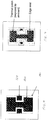
- FIG. 6 is a basic conceptual drawing of the OLED device 100 in which an organic layer 200 is received between the cathode 202 and anode 204, and received on a substrate 206.
- a first thermal management aspect is to manipulate the cathode 202 itself.
- the cathode has a thickness on the order of 100 nm. It is proposed to make the cathode up to 500 nm thick, and possibly between 1000 - 2000 nm thick. Generally, the limit for the cathode thickness is between 500 nm and 1000 nm where the constraint regarding the thickness of this layer relates to the reality of the manufacturing process. That is, a vapor deposition process is typically used to put down the cathode layer and applying extremely thick materials would take a long time. For a single layer cathode, a 500 nm or greater thickness provides a means to manage the thermals in the device.
- thermal management is at least in part dependent on the material used to construct the cathode, or in some instances the cathode is formed of multiple materials or metal alloys, or the cathode may have distinct, separate layers, of varying thickness.
- preferred metal cathode materials include the group of silicon (Si), tin (Sn), antimony (Sb), copper (Cu), nickel (Ni), molybdenum (Mo), aluminum (Al), silver (Ag), and zinc (Zn).
- the cathode selection may be based in part on thermal conductivity or rigidity modulus.
- the following table illustrates the thermal conductivity and rigidity modulus, of cathodes that could be used in OLED devices of large area, flexible assemblies.
- Metal Thermal Rigidity Modulus Conductivity (W/mK) GPa) Silicon (Si) 150 110 Tin (Sn) 67 18 Antimony (Sb) 24 20 Nickel (Ni) 91 76 Molybdenum (Mb) 139 20 Zinc (Zn) 120 43 Copper (Cu) 401 48 Aluminum (Al) 236 26 Silver (Ag) 430 30
- the cathode 202 may have a thickness of approximately 500 nm, and may range in thickness from approximately 1000 nm to preferably no greater than approximately 2000 nm. These thicknesses are associated with operating the OLED between a range of approximately 1 W to less than 60 W, and more preferably in a range from approximately 1 to approximately 10 W.
- the rigidity modulus may range from approximately 15 (tin) to approximately 110 (silicon) GPa to ensure flexibility of the OLED device.
- the thermal conductivity may range from approximately 20 (antimony) to 430 (silver) W/mK.
- the preferred thickness t and thermal conductivity k of the cathode 202 can be understood from the following description of the heat dissipation from the cathode 202 to the ambient air.
- the uniform heat load generally does not overheat the OLED structures.
- the power density of an OLED is typically about 1 Watt per 0.01 m2, so P/A O ⁇ 100 W/m 2 .
- the temperature rise due to the uniform heat dissipation is negligible, and does not create a limit on the thickness or thermal conductivity of the cathode 202 or any of the other planar OLED layers having similar dimensions. Even for a value of k ⁇ 0.1 W/m-K, the allowable thickness of a layer is any t ⁇ 10 mm.
- Equation 2 expresses the thermal power dissipated by free convection to ambient air.
- ⁇ ⁇ T P / A O ⁇ l / h
- the convection coefficient h for flat surfaces in contact with air varies as a function of vertical or horizontal orientation, surface figure, and other factors, but is typically ⁇ 10 W/m 2 K.
- the result of Equation 2 is ⁇ T ⁇ 10 K, which is generally an allowable temperature increase above ambient for the OLED.
- the results of Equations 1 and 2 indicate that the heating of the OLED due to uniform heat loading ⁇ 100 W/m 2 results in a uniform temperature increase of the OLED relative to ambient air of ⁇ 10 K, limited by free convection to ambient air, as long as none of the OLED layers has a ratio of t/k ⁇ 0.1 K m 2 /W. This typically allows for thickness t up to as much as 10 mm even for k as small as 0.1 W/m-K.
- the uniform heat load generally does not overheat the OLED structures.
- Equation 2 still applies, with the substitution of total OLED power P by the local hot spot power P local .
- Equation 1 must be replaced by Equation 3, where the limiting thermal conduction path is no longer the thickness t across the layer(s), but rather is determined by the need to spread the heat away from the hot spot, parallel to the OLED layer(s) along a length L.
- Equation 3 P local / A X ⁇ L / k
- the length L across which the heat must be conducted is much longer than the thickness t, and the cross-sectional area AX through which the heat is conducted is much less than the surface area A O , of any given OLED layer(s), for example the cathode 202. So, the requirement on thickness t and thermal conductivity k of the OLED layer(s) are much more demanding than for the uniform heat load. Since the case of uniform heat load generates a temperature increase ⁇ 10 K on the OLED relative to ambient air, and since an additional temperature rise due to local heating should be limited to an additional ⁇ 10 K, or at most ⁇ 50 K, then the heat from the local hot spot must be dissipated by convection to air over a relatively large surface area A S ⁇ L 2 .
- Equation (3) The effective cross-sectional area of the OLED layer, for example the cathode 202, through which the heat is conducted away from the hot spot is A X ⁇ t ⁇ L. Then Equation (3) simplifies to Equation (4), which is independent of L, as expected. ⁇ ⁇ T ⁇ P local / t ⁇ k
- the value of k should be ⁇ 100 W/m-K or greater, or a significant fraction of 100 W/m-K, and the value of t should be ⁇ 1 micron, or greater, or a significant fraction of 1 micron, in order to limit the additional heating at a local hot spot to ⁇ 10 K, or at most ⁇ 50 K, for the case where the non-uniformity of the heating is ⁇ 0.1% of the total OLED power, which might represent a typical ohmic loss at the electrical contacts, for example.
- the cathode 202 is constructed in a bi-layer fashion (as represented by the dashed line 210 in Figure 6 .
- the layer closest to the functional organic layers 200 within the OLED 100 is constructed of a thin, preferably ⁇ 50nm layer, Al or Ag, and the remainder of the cathode, up to 2000nm but more preferably around 450 nm, is constructed from a different material from the table.
- a bilayer cathode one is able to maximize the electron injection properties and/or reflective properties by choosing a compatible material for the thin inner layer, in addition to being able to separately tailor the thermal conductivity and flex capabilities of the cathode with the thick outer layer.
- the protective cover prevents handling damage and can also provide an additional oxygen and moisture barrier. If a protective cover is utilized, it is also beneficial to ensure that the generated heat in the OLED device can be transferred through that layer as well. This can be accomplished by choosing to make the protective cover out of materials that have high thermal conductivity.
- the protective cover is an electrical insulator, exhibits thermal conductivities greater than 5 W/(mk), and has a thickness of less than 75 micrometers.
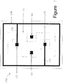
- Figure 7 illustrates one manner of directing heat transfer to a perimeter by way of a heat dissipation trace. More specifically, the backside of the OLED panel illustrates electrical feedthroughs 120 that are used with the flexible cable 122 (removed for ease of illustration in Figure 7 ) and that interconnect with an associated drive circuit. Electrically isolated, and preferably dimensionally spaced from the electrical feedthroughs are additional feedthroughs referred to as thermal sink feedthroughs 150.
- the thermal feedthroughs are preferably spaced inwardly of the perimeter and are formed of a thermally conductive material in order to convey heat from a central portion of the backside of the OLED panel via traces 152 that interconnect the thermal sink feedthroughs 150 with a perimeter heat dissipation trace 154.
- the representation in Figure 5 is just one preferred arrangement of the thermal sink feedthroughs, interconnecting traces, and heat dissipation traces. That is, one skilled in the art will recognize that other designs can be used without departing from the scope and intent of the present disclosure.
- the heat dissipation traces are preferably located along the perimeter of the OLED panel where the traces are in thermally conductive relation with an associated fixture (not shown) to convey away as much heat as possible that is generated by operation of the OLED device.
- the traces form a pathway to convey heat from the central portion of the panel and into the fixture where the heat is effectively dissipated by convection to the surrounding environment or the large thermal mass of the fixture will be sufficient to serve as an effective heat sink.
- a preferred material to assist with thermal conduction is a high thermal conductivity adhesive, for example, commercially available adhesives that exhibit a thermal conductivity of approximately 1.0 - 5.0 W/mK.
- the adhesive may be utilized to more effectively transfer heat out of the system where adhesive bonding is necessary.
- Examples of where the adhesive may be located include, but are not limited to, between the light emitting device and the thermal feedthroughs 150, between the thermal feedthroughs 150 and the trace 152, and between the traces 152/154 and the thermal sink fixture.
- the number, size, and location of thermal feedthroughs can be optimized based on the device or the end use/application.
- the traces shown in Figure 5 transfer the heat away from the OLED device, toward the edge seal region. Again, the trace dimensions and designs can also be optimized for the device/application.
- traces may not be needed if the OLED panel can be effectively heat sinked to the fixture itself via the thermal feedthroughs. However, at least in some applications, it would likely be advantageous to simply move the heat toward the edges the panel and away from the OLED devices.
- the high thermal conductivity of the adhesive on the backside of the OLED device effectively transfers the heat away from the device to the metal patch thermal feedthroughs.
- the adhesive has a thermal conductivity that is about an order of magnitude higher than that of typical polymers, and so the adhesive should effectively transfer the heat to the thermal feedthroughs.
- the adhesive is thin (on the order of approximately 10-100 ⁇ m) and flexible, the use of the thermally conductive adhesive does not adversely impact on the desire to provide a flexible, thin OLED panel. Further, it is preferable that the OLED devices are adhered to the backsheet for mechanical reasons. For example, air pockets are not desirable in the OLED assembly. Therefore, the adhesive can serve the added function of mechanically adhering the OLED device to the backsheet for those designs that do not already have an adhesive on the backsheet.
- the traces illustrated in Figure 7 are also preferably made of thin, thermally conductive material, such as those presented in the Table.
- the thickness range is from approximately 10-100 ⁇ m, and the traces are adhered to the external surface of the backsheet using conventional adhesives.
- the width of the traces can vary depending on the size and power of the OLED, but widths of 1-15 mm are common. These material and geometry characteristics will allow effective heat dissipation without inhibiting the flexibility of the device.
- Embodiments illustrated in Figures 8-9 and 10-11 show two more thermally managed backsheet designs for the OLED assembly.
- the thermal contact patches 160 shown in Figures8-9 illustrate how the thermal contact patches can be substantially enlarged to provide support for substantially the entire backside of the OLED.
- This enlarged patch eliminates stress concentrations that arise in designs where electrical patches only are provided to electrically connect the OLED panel through the backside as taught in US 2011/0147768 A1 .
- this large metallic surface that is coupled to the OLED device with thermally conductive adhesive is also exposed on the external surface. This allows a large surface area for convection to dissipate heat generated in the panel, as a large area pathway of thermally conductive material is incorporated from the device to the outside environment.
- the exposed metal on the backside should be at least 30% of the area of the light emitting device that is internal to the panel.
- thin, thermally conductive materials will preferably be utilized as previously described in the application.
- a combined electrical/thermal patch 170 is provided and shown here as a pair of patches that are dimensionally spaced or electrically isolated from one another.
- the combined electrical/thermal patches cover a substantial portion of the surface area of the OLED panel. This provides the desired mechanical support, and also serves as an enlarged heat sink. It is contemplated that there may be multiple openings in the backsheet to connect and transfer heat or provide electrical continuity as required by the design.
- a third area of thermal management is achieved with heat sinking to a fixture/plate 180.
- a fixture/plate 180 Once heat is removed from the panel via the above described arrangements, convection on the external surface, or preferably a heat sink is provided such as fixture 180, such that conduction into a large thermal mass and convection are enhanced.
- Preferred fixture/plate materials are shown in the Table. The required thermal mass and exposed surface area of the fixture/plate to dissipate the generated heat is highly dependent on the application, and can be determined by considering numerous factors such as the number of light emitting devices, the operational power of the devices, the efficiency of the devices, the thermal conductivity of the fixture/plate, and the efficiency of the specific device thermal management and panel thermal management schemes utilized.
Landscapes
- Physics & Mathematics (AREA)
- Optics & Photonics (AREA)
- Electroluminescent Light Sources (AREA)
Applications Claiming Priority (2)
| Application Number | Priority Date | Filing Date | Title |
|---|---|---|---|
| US13/223,935 US8829556B2 (en) | 2011-09-01 | 2011-09-01 | Thermal management in large area flexible OLED assembly |
| PCT/US2012/052051 WO2013032854A1 (en) | 2011-09-01 | 2012-08-23 | Thermal management in large area flexible oled assembly |
Publications (2)
| Publication Number | Publication Date |
|---|---|
| EP2751856A1 EP2751856A1 (en) | 2014-07-09 |
| EP2751856B1 true EP2751856B1 (en) | 2020-04-08 |
Family
ID=46981072
Family Applications (1)
| Application Number | Title | Priority Date | Filing Date |
|---|---|---|---|
| EP12769199.6A Active EP2751856B1 (en) | 2011-09-01 | 2012-08-23 | Thermal management in large area flexible oled assembly |
Country Status (7)
Families Citing this family (14)
| Publication number | Priority date | Publication date | Assignee | Title |
|---|---|---|---|---|
| DE102012109238A1 (de) * | 2012-09-28 | 2014-04-03 | Osram Opto Semiconductors Gmbh | Optoelektronisches Bauelement und Verfahren zum Herstellen eines optoelektronischen Bauelementes |
| DE102013108871A1 (de) * | 2013-08-16 | 2015-03-12 | Osram Opto Semiconductors Gmbh | Organisches Licht emittierendes Bauelement |
| KR102107622B1 (ko) * | 2013-09-06 | 2020-05-07 | 엘지이노텍 주식회사 | 조명장치 |
| DE102014205747A1 (de) * | 2014-03-27 | 2015-10-01 | Tridonic Gmbh & Co Kg | Leuchtmodul und Herstellungsverfahren für ein Leuchtmodul |
| CN104021735B (zh) * | 2014-05-23 | 2016-08-17 | 京东方科技集团股份有限公司 | 一种量子点发光显示屏及其制备方法 |
| DE102015105484B4 (de) * | 2015-01-13 | 2025-08-21 | Pictiva Displays International Limited | Organisches Licht emittierendes Bauelement |
| CN104701353A (zh) * | 2015-03-27 | 2015-06-10 | 京东方科技集团股份有限公司 | 有机发光显示面板和显示装置 |
| CN106328680B (zh) * | 2016-08-25 | 2019-03-15 | 昆山国显光电有限公司 | 有机发光显示装置的激光密封导热治具及激光密封方法 |
| CN107195795B (zh) * | 2017-06-07 | 2019-06-14 | 武汉天马微电子有限公司 | 可折叠显示面板和可折叠显示装置 |
| US10369774B2 (en) | 2017-06-30 | 2019-08-06 | Microsoft Technology Licensing, Llc | Thermally conductive de-bonding aid |
| KR102565415B1 (ko) * | 2018-02-21 | 2023-08-09 | 삼성디스플레이 주식회사 | 표시 장치 |
| CN108760144A (zh) * | 2018-05-29 | 2018-11-06 | 成都新柯力化工科技有限公司 | 一种提高压力电子传感器灵敏度的柔性膜 |
| US11084955B2 (en) | 2018-07-23 | 2021-08-10 | Microsoft Technology Licensing, Llc | Pressure sensitive adhesive with thermally conductive release tab |
| KR102772788B1 (ko) | 2020-02-26 | 2025-02-26 | 삼성디스플레이 주식회사 | 표시 장치 |
Family Cites Families (32)
| Publication number | Priority date | Publication date | Assignee | Title |
|---|---|---|---|---|
| JP2001318627A (ja) | 2000-02-29 | 2001-11-16 | Semiconductor Energy Lab Co Ltd | 発光装置 |
| JP4599685B2 (ja) | 2000-08-04 | 2010-12-15 | ソニー株式会社 | 平面表示素子 |
| US6819316B2 (en) | 2001-04-17 | 2004-11-16 | 3M Innovative Properties Company | Flexible capacitive touch sensor |
| JP2003109773A (ja) | 2001-07-27 | 2003-04-11 | Semiconductor Energy Lab Co Ltd | 発光装置、半導体装置およびそれらの作製方法 |
| US20040035360A1 (en) | 2002-05-17 | 2004-02-26 | Semiconductor Energy Laboratory Co., Ltd. | Manufacturing apparatus |
| TW577242B (en) | 2002-08-19 | 2004-02-21 | Ritdisplay Corp | Organic light emitting panel and method of manufacturing the same |
| US7344901B2 (en) | 2003-04-16 | 2008-03-18 | Corning Incorporated | Hermetically sealed package and method of fabricating of a hermetically sealed package |
| US6998776B2 (en) | 2003-04-16 | 2006-02-14 | Corning Incorporated | Glass package that is hermetically sealed with a frit and method of fabrication |
| US7227196B2 (en) | 2003-05-20 | 2007-06-05 | Burgener Ii Robert H | Group II-VI semiconductor devices |
| US7172813B2 (en) | 2003-05-20 | 2007-02-06 | Burgener Ii Robert H | Zinc oxide crystal growth substrate |
| US7141489B2 (en) | 2003-05-20 | 2006-11-28 | Burgener Ii Robert H | Fabrication of p-type group II-VI semiconductors |
| US7161173B2 (en) | 2003-05-20 | 2007-01-09 | Burgener Ii Robert H | P-type group II-VI semiconductor compounds |
| US6967439B2 (en) | 2004-02-24 | 2005-11-22 | Eastman Kodak Company | OLED display having thermally conductive backplate |
| US7393598B2 (en) | 2004-03-10 | 2008-07-01 | Hcf Partners, L.P. | Light emitting molecules and organic light emitting devices including light emitting molecules |
| US7205718B2 (en) | 2004-06-24 | 2007-04-17 | Eastman Kodak Company | OLED display having thermally conductive adhesive |
| US20050285518A1 (en) | 2004-06-24 | 2005-12-29 | Eastman Kodak Company | OLED display having thick cathode |
| US7205717B2 (en) | 2004-06-24 | 2007-04-17 | Eastman Kodak Company | OLED display having thermally conductive material |
| US7583022B2 (en) | 2004-08-02 | 2009-09-01 | Eastman Kodak Company | OLED display with electrode |
| JP2006107755A (ja) | 2004-09-30 | 2006-04-20 | Seiko Epson Corp | 電気光学装置、画像形成装置および画像読み取り装置 |
| TWI268732B (en) * | 2004-12-16 | 2006-12-11 | Au Optronics Corp | Organic light emitting device |
| JP2006196271A (ja) | 2005-01-12 | 2006-07-27 | Fuji Electric Holdings Co Ltd | 有機el素子およびその製造方法 |
| KR20070103204A (ko) | 2006-04-18 | 2007-10-23 | 주식회사 동진쎄미켐 | 우수한 열전도도를 갖는 광경화성 수지 조성물 |
| TWI331483B (en) | 2006-08-07 | 2010-10-01 | Ritdisplay Corp | Organic light emitting device with heat dissipation structure |
| JP2008289124A (ja) | 2007-04-17 | 2008-11-27 | Hitachi Ltd | アクティブマトリクスディスプレイを備えたテレビジョン装置 |
| TWI341599B (en) * | 2007-06-06 | 2011-05-01 | Chipmos Technoligies Inc | Light source module and the method for adjusting the brightness thereof |
| JP5541872B2 (ja) * | 2009-02-26 | 2014-07-09 | パナソニック株式会社 | 面状発光装置および照明器具 |
| TWI587734B (zh) * | 2009-03-26 | 2017-06-11 | 精工愛普生股份有限公司 | 有機el裝置、有機el裝置之製造方法、及電子機器 |
| US20100294526A1 (en) | 2009-05-21 | 2010-11-25 | General Electric Company | Hermetic electrical package |
| JP5501687B2 (ja) * | 2009-07-27 | 2014-05-28 | パナソニック株式会社 | 有機el光源ユニット |
| JP2011076844A (ja) * | 2009-09-30 | 2011-04-14 | Sumitomo Chemical Co Ltd | 発光装置 |
| US8710732B2 (en) | 2009-12-22 | 2014-04-29 | General Electric Company | Organic light emitting device connection methods |
| US8253329B2 (en) | 2010-01-21 | 2012-08-28 | General Electric Company | Enhanced edge seal design for organic light emitting diode (OLED) encapsulation |
-
2011
- 2011-09-01 US US13/223,935 patent/US8829556B2/en active Active
-
2012
- 2012-08-23 JP JP2014528465A patent/JP6189298B2/ja active Active
- 2012-08-23 WO PCT/US2012/052051 patent/WO2013032854A1/en unknown
- 2012-08-23 KR KR1020147005642A patent/KR101983740B1/ko active Active
- 2012-08-23 EP EP12769199.6A patent/EP2751856B1/en active Active
- 2012-08-23 CN CN201280042358.XA patent/CN103782409B/zh active Active
- 2012-08-31 TW TW101131933A patent/TWI560920B/zh active
Non-Patent Citations (1)
| Title |
|---|
| None * |
Also Published As
| Publication number | Publication date |
|---|---|
| CN103782409B (zh) | 2016-10-12 |
| WO2013032854A1 (en) | 2013-03-07 |
| CN103782409A (zh) | 2014-05-07 |
| JP6189298B2 (ja) | 2017-08-30 |
| US20130056783A1 (en) | 2013-03-07 |
| KR20140067020A (ko) | 2014-06-03 |
| TW201316587A (zh) | 2013-04-16 |
| US8829556B2 (en) | 2014-09-09 |
| KR101983740B1 (ko) | 2019-05-29 |
| JP2014525661A (ja) | 2014-09-29 |
| EP2751856A1 (en) | 2014-07-09 |
| TWI560920B (en) | 2016-12-01 |
Similar Documents
| Publication | Publication Date | Title |
|---|---|---|
| EP2751856B1 (en) | Thermal management in large area flexible oled assembly | |
| US7205718B2 (en) | OLED display having thermally conductive adhesive | |
| JP5541872B2 (ja) | 面状発光装置および照明器具 | |
| JP4499672B2 (ja) | 有機el素子及びその製造方法 | |
| US8344389B2 (en) | Optoelectronic device array | |
| CN103262651B (zh) | 带有电流传播总线的大面积发光电封装 | |
| US7205717B2 (en) | OLED display having thermally conductive material | |
| JP2011204692A (ja) | 熱伝導性背面プレートを備えるoledディスプレイ | |
| JP5695312B2 (ja) | 有機el装置 | |
| TW201244524A (en) | Organic light emitting diode lighting apparatus | |
| US8766517B2 (en) | Organic light emitting device with conducting cover | |
| KR20110050985A (ko) | 유기전계발광소자 | |
| WO2014027395A1 (ja) | 有機el素子を用いた発光装置 | |
| CN120201856A (zh) | 钙钛矿太阳能电池 | |
| CN113972338A (zh) | 散热复合件和包括其的显示设备 |
Legal Events
| Date | Code | Title | Description |
|---|---|---|---|
| PUAI | Public reference made under article 153(3) epc to a published international application that has entered the european phase |
Free format text: ORIGINAL CODE: 0009012 |
|
| 17P | Request for examination filed |
Effective date: 20140401 |
|
| AK | Designated contracting states |
Kind code of ref document: A1 Designated state(s): AL AT BE BG CH CY CZ DE DK EE ES FI FR GB GR HR HU IE IS IT LI LT LU LV MC MK MT NL NO PL PT RO RS SE SI SK SM TR |
|
| DAX | Request for extension of the european patent (deleted) | ||
| 17Q | First examination report despatched |
Effective date: 20141208 |
|
| RAP1 | Party data changed (applicant data changed or rights of an application transferred) |
Owner name: BOE TECHNOLOGY GROUP CO., LTD. |
|
| STAA | Information on the status of an ep patent application or granted ep patent |
Free format text: STATUS: EXAMINATION IS IN PROGRESS |
|
| GRAP | Despatch of communication of intention to grant a patent |
Free format text: ORIGINAL CODE: EPIDOSNIGR1 |
|
| STAA | Information on the status of an ep patent application or granted ep patent |
Free format text: STATUS: GRANT OF PATENT IS INTENDED |
|
| INTG | Intention to grant announced |
Effective date: 20191029 |
|
| GRAS | Grant fee paid |
Free format text: ORIGINAL CODE: EPIDOSNIGR3 |
|
| GRAA | (expected) grant |
Free format text: ORIGINAL CODE: 0009210 |
|
| STAA | Information on the status of an ep patent application or granted ep patent |
Free format text: STATUS: THE PATENT HAS BEEN GRANTED |
|
| AK | Designated contracting states |
Kind code of ref document: B1 Designated state(s): AL AT BE BG CH CY CZ DE DK EE ES FI FR GB GR HR HU IE IS IT LI LT LU LV MC MK MT NL NO PL PT RO RS SE SI SK SM TR |
|
| REG | Reference to a national code |
Ref country code: GB Ref legal event code: FG4D |
|
| REG | Reference to a national code |
Ref country code: CH Ref legal event code: EP Ref country code: AT Ref legal event code: REF Ref document number: 1255563 Country of ref document: AT Kind code of ref document: T Effective date: 20200415 |
|
| REG | Reference to a national code |
Ref country code: IE Ref legal event code: FG4D |
|
| REG | Reference to a national code |
Ref country code: DE Ref legal event code: R096 Ref document number: 602012069141 Country of ref document: DE |
|
| REG | Reference to a national code |
Ref country code: NL Ref legal event code: MP Effective date: 20200408 |
|
| REG | Reference to a national code |
Ref country code: LT Ref legal event code: MG4D |
|
| PG25 | Lapsed in a contracting state [announced via postgrant information from national office to epo] |
Ref country code: SE Free format text: LAPSE BECAUSE OF FAILURE TO SUBMIT A TRANSLATION OF THE DESCRIPTION OR TO PAY THE FEE WITHIN THE PRESCRIBED TIME-LIMIT Effective date: 20200408 Ref country code: NL Free format text: LAPSE BECAUSE OF FAILURE TO SUBMIT A TRANSLATION OF THE DESCRIPTION OR TO PAY THE FEE WITHIN THE PRESCRIBED TIME-LIMIT Effective date: 20200408 Ref country code: LT Free format text: LAPSE BECAUSE OF FAILURE TO SUBMIT A TRANSLATION OF THE DESCRIPTION OR TO PAY THE FEE WITHIN THE PRESCRIBED TIME-LIMIT Effective date: 20200408 Ref country code: PT Free format text: LAPSE BECAUSE OF FAILURE TO SUBMIT A TRANSLATION OF THE DESCRIPTION OR TO PAY THE FEE WITHIN THE PRESCRIBED TIME-LIMIT Effective date: 20200817 Ref country code: FI Free format text: LAPSE BECAUSE OF FAILURE TO SUBMIT A TRANSLATION OF THE DESCRIPTION OR TO PAY THE FEE WITHIN THE PRESCRIBED TIME-LIMIT Effective date: 20200408 Ref country code: NO Free format text: LAPSE BECAUSE OF FAILURE TO SUBMIT A TRANSLATION OF THE DESCRIPTION OR TO PAY THE FEE WITHIN THE PRESCRIBED TIME-LIMIT Effective date: 20200708 Ref country code: GR Free format text: LAPSE BECAUSE OF FAILURE TO SUBMIT A TRANSLATION OF THE DESCRIPTION OR TO PAY THE FEE WITHIN THE PRESCRIBED TIME-LIMIT Effective date: 20200709 Ref country code: IS Free format text: LAPSE BECAUSE OF FAILURE TO SUBMIT A TRANSLATION OF THE DESCRIPTION OR TO PAY THE FEE WITHIN THE PRESCRIBED TIME-LIMIT Effective date: 20200808 |
|
| REG | Reference to a national code |
Ref country code: AT Ref legal event code: MK05 Ref document number: 1255563 Country of ref document: AT Kind code of ref document: T Effective date: 20200408 |
|
| PG25 | Lapsed in a contracting state [announced via postgrant information from national office to epo] |
Ref country code: LV Free format text: LAPSE BECAUSE OF FAILURE TO SUBMIT A TRANSLATION OF THE DESCRIPTION OR TO PAY THE FEE WITHIN THE PRESCRIBED TIME-LIMIT Effective date: 20200408 Ref country code: HR Free format text: LAPSE BECAUSE OF FAILURE TO SUBMIT A TRANSLATION OF THE DESCRIPTION OR TO PAY THE FEE WITHIN THE PRESCRIBED TIME-LIMIT Effective date: 20200408 Ref country code: BG Free format text: LAPSE BECAUSE OF FAILURE TO SUBMIT A TRANSLATION OF THE DESCRIPTION OR TO PAY THE FEE WITHIN THE PRESCRIBED TIME-LIMIT Effective date: 20200708 Ref country code: RS Free format text: LAPSE BECAUSE OF FAILURE TO SUBMIT A TRANSLATION OF THE DESCRIPTION OR TO PAY THE FEE WITHIN THE PRESCRIBED TIME-LIMIT Effective date: 20200408 |
|
| PG25 | Lapsed in a contracting state [announced via postgrant information from national office to epo] |
Ref country code: AL Free format text: LAPSE BECAUSE OF FAILURE TO SUBMIT A TRANSLATION OF THE DESCRIPTION OR TO PAY THE FEE WITHIN THE PRESCRIBED TIME-LIMIT Effective date: 20200408 |
|
| REG | Reference to a national code |
Ref country code: DE Ref legal event code: R097 Ref document number: 602012069141 Country of ref document: DE |
|
| PG25 | Lapsed in a contracting state [announced via postgrant information from national office to epo] |
Ref country code: RO Free format text: LAPSE BECAUSE OF FAILURE TO SUBMIT A TRANSLATION OF THE DESCRIPTION OR TO PAY THE FEE WITHIN THE PRESCRIBED TIME-LIMIT Effective date: 20200408 Ref country code: CZ Free format text: LAPSE BECAUSE OF FAILURE TO SUBMIT A TRANSLATION OF THE DESCRIPTION OR TO PAY THE FEE WITHIN THE PRESCRIBED TIME-LIMIT Effective date: 20200408 Ref country code: DK Free format text: LAPSE BECAUSE OF FAILURE TO SUBMIT A TRANSLATION OF THE DESCRIPTION OR TO PAY THE FEE WITHIN THE PRESCRIBED TIME-LIMIT Effective date: 20200408 Ref country code: ES Free format text: LAPSE BECAUSE OF FAILURE TO SUBMIT A TRANSLATION OF THE DESCRIPTION OR TO PAY THE FEE WITHIN THE PRESCRIBED TIME-LIMIT Effective date: 20200408 Ref country code: EE Free format text: LAPSE BECAUSE OF FAILURE TO SUBMIT A TRANSLATION OF THE DESCRIPTION OR TO PAY THE FEE WITHIN THE PRESCRIBED TIME-LIMIT Effective date: 20200408 Ref country code: AT Free format text: LAPSE BECAUSE OF FAILURE TO SUBMIT A TRANSLATION OF THE DESCRIPTION OR TO PAY THE FEE WITHIN THE PRESCRIBED TIME-LIMIT Effective date: 20200408 Ref country code: IT Free format text: LAPSE BECAUSE OF FAILURE TO SUBMIT A TRANSLATION OF THE DESCRIPTION OR TO PAY THE FEE WITHIN THE PRESCRIBED TIME-LIMIT Effective date: 20200408 Ref country code: SM Free format text: LAPSE BECAUSE OF FAILURE TO SUBMIT A TRANSLATION OF THE DESCRIPTION OR TO PAY THE FEE WITHIN THE PRESCRIBED TIME-LIMIT Effective date: 20200408 |
|
| PLBE | No opposition filed within time limit |
Free format text: ORIGINAL CODE: 0009261 |
|
| STAA | Information on the status of an ep patent application or granted ep patent |
Free format text: STATUS: NO OPPOSITION FILED WITHIN TIME LIMIT |
|
| PG25 | Lapsed in a contracting state [announced via postgrant information from national office to epo] |
Ref country code: PL Free format text: LAPSE BECAUSE OF FAILURE TO SUBMIT A TRANSLATION OF THE DESCRIPTION OR TO PAY THE FEE WITHIN THE PRESCRIBED TIME-LIMIT Effective date: 20200408 Ref country code: SK Free format text: LAPSE BECAUSE OF FAILURE TO SUBMIT A TRANSLATION OF THE DESCRIPTION OR TO PAY THE FEE WITHIN THE PRESCRIBED TIME-LIMIT Effective date: 20200408 |
|
| 26N | No opposition filed |
Effective date: 20210112 |
|
| PG25 | Lapsed in a contracting state [announced via postgrant information from national office to epo] |
Ref country code: MC Free format text: LAPSE BECAUSE OF FAILURE TO SUBMIT A TRANSLATION OF THE DESCRIPTION OR TO PAY THE FEE WITHIN THE PRESCRIBED TIME-LIMIT Effective date: 20200408 |
|
| REG | Reference to a national code |
Ref country code: CH Ref legal event code: PL |
|
| GBPC | Gb: european patent ceased through non-payment of renewal fee |
Effective date: 20200823 |
|
| PG25 | Lapsed in a contracting state [announced via postgrant information from national office to epo] |
Ref country code: CH Free format text: LAPSE BECAUSE OF NON-PAYMENT OF DUE FEES Effective date: 20200831 Ref country code: LI Free format text: LAPSE BECAUSE OF NON-PAYMENT OF DUE FEES Effective date: 20200831 Ref country code: LU Free format text: LAPSE BECAUSE OF NON-PAYMENT OF DUE FEES Effective date: 20200823 |
|
| REG | Reference to a national code |
Ref country code: BE Ref legal event code: MM Effective date: 20200831 |
|
| PG25 | Lapsed in a contracting state [announced via postgrant information from national office to epo] |
Ref country code: SI Free format text: LAPSE BECAUSE OF FAILURE TO SUBMIT A TRANSLATION OF THE DESCRIPTION OR TO PAY THE FEE WITHIN THE PRESCRIBED TIME-LIMIT Effective date: 20200408 |
|
| PG25 | Lapsed in a contracting state [announced via postgrant information from national office to epo] |
Ref country code: FR Free format text: LAPSE BECAUSE OF NON-PAYMENT OF DUE FEES Effective date: 20200831 |
|
| PG25 | Lapsed in a contracting state [announced via postgrant information from national office to epo] |
Ref country code: IE Free format text: LAPSE BECAUSE OF NON-PAYMENT OF DUE FEES Effective date: 20200823 Ref country code: GB Free format text: LAPSE BECAUSE OF NON-PAYMENT OF DUE FEES Effective date: 20200823 Ref country code: BE Free format text: LAPSE BECAUSE OF NON-PAYMENT OF DUE FEES Effective date: 20200831 |
|
| PG25 | Lapsed in a contracting state [announced via postgrant information from national office to epo] |
Ref country code: TR Free format text: LAPSE BECAUSE OF FAILURE TO SUBMIT A TRANSLATION OF THE DESCRIPTION OR TO PAY THE FEE WITHIN THE PRESCRIBED TIME-LIMIT Effective date: 20200408 Ref country code: MT Free format text: LAPSE BECAUSE OF FAILURE TO SUBMIT A TRANSLATION OF THE DESCRIPTION OR TO PAY THE FEE WITHIN THE PRESCRIBED TIME-LIMIT Effective date: 20200408 Ref country code: CY Free format text: LAPSE BECAUSE OF FAILURE TO SUBMIT A TRANSLATION OF THE DESCRIPTION OR TO PAY THE FEE WITHIN THE PRESCRIBED TIME-LIMIT Effective date: 20200408 |
|
| PG25 | Lapsed in a contracting state [announced via postgrant information from national office to epo] |
Ref country code: MK Free format text: LAPSE BECAUSE OF FAILURE TO SUBMIT A TRANSLATION OF THE DESCRIPTION OR TO PAY THE FEE WITHIN THE PRESCRIBED TIME-LIMIT Effective date: 20200408 |
|
| REG | Reference to a national code |
Ref country code: DE Ref legal event code: R079 Ref document number: 602012069141 Country of ref document: DE Free format text: PREVIOUS MAIN CLASS: H01L0051520000 Ipc: H10K0050800000 |
|
| PGFP | Annual fee paid to national office [announced via postgrant information from national office to epo] |
Ref country code: DE Payment date: 20240819 Year of fee payment: 13 |