EP2747518A1 - Apparatus for driving light emitting diode array and liquid crystal display device using the same - Google Patents
Apparatus for driving light emitting diode array and liquid crystal display device using the same Download PDFInfo
- Publication number
- EP2747518A1 EP2747518A1 EP13193774.0A EP13193774A EP2747518A1 EP 2747518 A1 EP2747518 A1 EP 2747518A1 EP 13193774 A EP13193774 A EP 13193774A EP 2747518 A1 EP2747518 A1 EP 2747518A1
- Authority
- EP
- European Patent Office
- Prior art keywords
- led array
- current
- current amount
- external system
- amount setter
- Prior art date
- Legal status (The legal status is an assumption and is not a legal conclusion. Google has not performed a legal analysis and makes no representation as to the accuracy of the status listed.)
- Granted
Links
Images


Classifications
-
- G—PHYSICS
- G02—OPTICS
- G02F—OPTICAL DEVICES OR ARRANGEMENTS FOR THE CONTROL OF LIGHT BY MODIFICATION OF THE OPTICAL PROPERTIES OF THE MEDIA OF THE ELEMENTS INVOLVED THEREIN; NON-LINEAR OPTICS; FREQUENCY-CHANGING OF LIGHT; OPTICAL LOGIC ELEMENTS; OPTICAL ANALOGUE/DIGITAL CONVERTERS
- G02F1/00—Devices or arrangements for the control of the intensity, colour, phase, polarisation or direction of light arriving from an independent light source, e.g. switching, gating or modulating; Non-linear optics
- G02F1/01—Devices or arrangements for the control of the intensity, colour, phase, polarisation or direction of light arriving from an independent light source, e.g. switching, gating or modulating; Non-linear optics for the control of the intensity, phase, polarisation or colour
- G02F1/13—Devices or arrangements for the control of the intensity, colour, phase, polarisation or direction of light arriving from an independent light source, e.g. switching, gating or modulating; Non-linear optics for the control of the intensity, phase, polarisation or colour based on liquid crystals, e.g. single liquid crystal display cells
- G02F1/133—Constructional arrangements; Operation of liquid crystal cells; Circuit arrangements
- G02F1/1333—Constructional arrangements; Manufacturing methods
- G02F1/1335—Structural association of cells with optical devices, e.g. polarisers or reflectors
- G02F1/1336—Illuminating devices
- G02F1/133602—Direct backlight
- G02F1/133603—Direct backlight with LEDs
-
- H—ELECTRICITY
- H05—ELECTRIC TECHNIQUES NOT OTHERWISE PROVIDED FOR
- H05B—ELECTRIC HEATING; ELECTRIC LIGHT SOURCES NOT OTHERWISE PROVIDED FOR; CIRCUIT ARRANGEMENTS FOR ELECTRIC LIGHT SOURCES, IN GENERAL
- H05B45/00—Circuit arrangements for operating light-emitting diodes [LED]
- H05B45/10—Controlling the intensity of the light
- H05B45/14—Controlling the intensity of the light using electrical feedback from LEDs or from LED modules
-
- H—ELECTRICITY
- H05—ELECTRIC TECHNIQUES NOT OTHERWISE PROVIDED FOR
- H05B—ELECTRIC HEATING; ELECTRIC LIGHT SOURCES NOT OTHERWISE PROVIDED FOR; CIRCUIT ARRANGEMENTS FOR ELECTRIC LIGHT SOURCES, IN GENERAL
- H05B45/00—Circuit arrangements for operating light-emitting diodes [LED]
- H05B45/40—Details of LED load circuits
- H05B45/44—Details of LED load circuits with an active control inside an LED matrix
-
- H—ELECTRICITY
- H05—ELECTRIC TECHNIQUES NOT OTHERWISE PROVIDED FOR
- H05B—ELECTRIC HEATING; ELECTRIC LIGHT SOURCES NOT OTHERWISE PROVIDED FOR; CIRCUIT ARRANGEMENTS FOR ELECTRIC LIGHT SOURCES, IN GENERAL
- H05B45/00—Circuit arrangements for operating light-emitting diodes [LED]
- H05B45/40—Details of LED load circuits
- H05B45/44—Details of LED load circuits with an active control inside an LED matrix
- H05B45/46—Details of LED load circuits with an active control inside an LED matrix having LEDs disposed in parallel lines
-
- H—ELECTRICITY
- H05—ELECTRIC TECHNIQUES NOT OTHERWISE PROVIDED FOR
- H05B—ELECTRIC HEATING; ELECTRIC LIGHT SOURCES NOT OTHERWISE PROVIDED FOR; CIRCUIT ARRANGEMENTS FOR ELECTRIC LIGHT SOURCES, IN GENERAL
- H05B47/00—Circuit arrangements for operating light sources in general, i.e. where the type of light source is not relevant
- H05B47/10—Controlling the light source
Definitions
- the disclosure relate to an apparatus for driving a light emitting diode (LED) array, and more particularly, to an apparatus for driving an LED array used as a backlight of a liquid crystal display (LCD) device and an LCD device using the same.
- LED light emitting diode
- Flat panel display devices are widely used for various electronic devices such as large-size digital televisions (TVs) requiring a reduction in weight and thickness as well as mobile devices which necessarily need a small size and low power.
- LCD devices are applied to all electronic products ranging from small-size devices to large-size devices, and thus are being most widely used.
- a light source called a backlight is disposed at a rear surface of the liquid crystal panel. Light emitted from the backlight is outputted to the outside through a liquid crystal layer and color filter of the liquid crystal panel, thereby enabling an image to be displayed by the liquid crystal panel.
- Cold cathode fluorescent lamps (CCFLs), external electrode fluorescent lamps (EEFLs), or the like are being widely used as the backlight.
- LEDs which are sufficiently high in luminance and are low in power consumption and manufacturing cost were developed to replace the above-described backlights. That is, since a backlight unit using an LED array does not use a high-cost diffusive film and does not need an inverter unlike fluorescent lamps, the manufacturing cost can be saved, a panel can be easily enlarged in size, a thickness and weight can be reduced, and power consumption and environmental problems can decrease. Accordingly, the backlight unit using the LED array is being widely used.
- a backlight unit using LEDs includes an LED array having a plurality of LED strings, each of which is configured with a plurality of LEDs.
- An amount of light emitted from an LED is proportional to a level of a driving current passing through an active layer of the LED.
- Driving of the LED denotes supplying and controlling a driving current which flows to the LED.
- FIG. 1 is an example diagram illustrating a configuration of a related art apparatus for driving an LED array 60.
- a related art apparatus 50 for driving an LED array 60 includes: a control unit 51 that supplies power to an LED array 60 by using an input voltage VIN received from an external source, and controls the amount of current to flow in the LED array 60; a current fixing unit 52 that provides a certain resistance to the control unit 51 in order for a certain amount of current to be supplied to the LED array 60; and a switching unit 53 that controls current flowing in the LED array 60 to vary a luminance of the LED array 60.
- the control unit 51 is generally configured as an integrated circuit (IC), and may be mounted on a main board of an LCD device together with a timing controller.
- the switching unit (current varying unit) 53 may be provided inside or outside the control unit 51.
- the current fixing unit 52 is disposed outside the control unit 51, and set to have a certain resistance value.
- the related art apparatus 50 for driving the LED array controls the luminance of the LED array 60, for controlling the power consumption of the LED array 60.
- the current fixing unit 52 is set to have an impedance value, which controls the maximum current supplied to the LED array 60 and thus enables the LED array 60 to output a luminance of 100%. Therefore, the control unit 51 continuously supplies a current having the maximum value to the LED array 60 by using the resistance value set by the current fixing unit 52 and the input voltage VIN supplied from an external system.
- the control unit 51 includes a power supplier 51a for supplying a voltage and a current to the LED array 60 by using the input voltage VIN and the maximum current.
- a current supplied to the LED array 60 is fixed to the maximum value by the current fixing unit 52, and the LED array 60 outputs the maximum luminance with the maximum current.
- the control unit 51 When the LED array 60 outputs light having the maximum luminance, an image displayed by a panel can be preferably sharpened. However, when the LED array 60 outputs light having the maximum luminance, energy consumption increases proportionally.
- the control unit 51 In order to decrease the amount of consumed energy, the control unit 51 generally uses a pulse width modulation (PWM) signal received from the external system.
- PWM pulse width modulation
- the control unit 51 includes a current amount controller 51b.
- the PWM signal is composed of pulses that have a constant cycle but vary in pulse width, and a turn-on time of a thin film transistor (TFT) configuring the switching unit 53 is controlled by the PWM signal.
- TFT thin film transistor
- the time during which the maximum current flows to the LED array 60 is controlled by controlling the turn-on time of the TFT, and thus, a luminance of the LED array 60 may be changed. For example, in dividing one pulse width by a cycle ratio, a high signal occupies 10% and a low signal occupies 90% when a ratio of 10%, and when a ratio of 70%, the high signal occupies 70% and the low signal occupies 30%.
- the PWM signal is generated at the ratio of 10%
- a high signal having a narrow pulse width is generated, and inputted to the switching unit 53 through the current amount controller 51b.
- the pulse width of the high signal is narrow, a time for which the TFT of the switching unit 53 is turned on is shortened, and thus, a time for which a current flows to the LED array 60 is shortened. Therefore, the luminance of the LED array 60 decreases.
- the PWM signal is generated at the ratio of 70%
- a high signal having a broad pulse width is generated, and inputted to the switching unit 53 through the current amount controller 51b.
- the pulse width of the high signal is broad, a time for which the TFT of the switching unit 53 is turned on is extended, and thus, a time for which a current flows to the LED array 60 is extended. Therefore, the luminance of the LED array 60 increases.
- Manufacturers of various electronic products such as notebook computers, TVs, tablet personal computers (PCs), etc., by using the above-described LCD device, may adjust the amplitude of the pulse width of the PWM signal sent to the control unit 51 to adjust the amount of power consumed by the LCD device and electronic product.
- a PWM signal having a narrow pulse width may be received at the current amount control unit 51b from the external system.
- a PWM signal having a broad pulse width may be received at the current amount control unit 51b from the external system. Accordingly, electronic products vary the pulse width of the PWM signal, and thus drive the LCD devices with desired power.
- the above-described LCD device of the related art has the following problems.
- the PWM signal must be received from the external system to the control unit 51, for adjusting the luminance of the LED array 60. Therefore, it is difficult for a manufacturer, which is unable to directly develop a PWM signal, to manufacture an electronic product by using the related art LCD device.
- the PWM signal for adjusting the luminance of the LED array 60 is required to be synchronized with the frame rate of the LCD device so as to prevent a wavy noise. Therefore, the external system which is driven in connection with the related art LCD device needs to include separate circuits for generating the PWM signal synchronized with the frame rate. For this reason, there is a limitation in developing and manufacturing the external system.
- Embodiments relate to an apparatus for driving a light emitting diode (LED) array.
- the apparatus includes a current amount setter and a controller coupled to the current amount setter and the LED array.
- the current amount setter varies a voltage at a node or a current in the node of the current amount setter according to a selection signal from an external system.
- the controller includes a power supplier and a signal supplier.
- the power supplier adjusts a level of current provided to the LED array based on an input voltage received from the external system and the resistance across the current amount setter.
- the signal supplier distributes direct current (DC) signals remaining unchanged during a frame cycle to a plurality of switches coupled to the LED array to turn on or off LEDs in the LED array.
- DC direct current
- Various embodiments provide an apparatus for driving a light emitting diode (LED), the apparatus comprising: a current amount setter configured to vary a voltage at a node or a current in the node of the current amount setter according to a selection signal from an external system; and a controller coupled to the current amount setter and the LED array, the controller comprising: a power supplier connected to the node of the current amount setter and configured to adjust a level of current provided to the LED array based on an input voltage received from the external system and the voltage at the node or the current in the node of the current amount setter, and a signal supplier configured to distribute direct current (DC) signals remaining unchanged during a frame cycle to a plurality of switches coupled to the LED array to turn on or off LEDs in the LED array.
- DC direct current
- the power supplier is configured to adjust the level of current provided to the LED array based on the input voltage received from the external system and a resistance across the current amount setter.
- the current amount setter comprises a selection terminal connected to the external system, a resistance across the current amount setter determined based on connection of the selection terminal to a high-level voltage terminal or a ground terminal through the external system or being maintained in a high impedance state.
- the current amount setter comprises a capacitor between the node and a low reference voltage; a transistor having a gate coupled to the selection terminal; a diode between a source of the transistor and the selection terminal; a first resistor between the source of the transistor and the node; a second resistor between the source of the transistor and the low reference voltage; and a third resistor between a drain of the transistor and the low reference voltage.
- the current amount setter comprises at least two selection terminals connected to a ground terminal or maintained in an high impedance state, a resistance across the current amount setter determined based on connection of the selection terminals to the ground terminal through the external system or being maintained in a high impedance state.
- the current amount setter comprises a string of resistors connected in parallel to a capacitor, each of the at least two selection terminals connected between the string of resistors.
- the plurality of switches are configured as switching transistors and are connected between a ground terminal and a plurality of LED strings in the LED array.
- the signal supplier is configured to distribute the DC signals to the plurality of switches responsive to receiving a DC signal from the external system.
- the LED array comprises a plurality of strings of LEDs, each string of LEDs coupled to a low reference voltage via each of the plurality of switches.
- a liquid crystal display (LCD) device including an apparatus for driving a light emitting diode (LED) array, the LCD device comprising: a panel in which a plurality of pixels are respectively formed in a plurality of areas defined by intersections between a plurality of gate lines and a plurality of data lines, the panel irradiated by light from the LED array; a driver configured to control signals to be supplied to the gate lines and the data lines; and an LED array driving apparatus according to any one of the embodiments described herein.
- LED light emitting diode
- a liquid crystal display (LCD) device including an apparatus for driving a light emitting diode (LED) array, the LCD device comprising: a panel in which a plurality of pixels are respectively formed in a plurality of areas defined by intersections between a plurality of gate lines and a plurality of data lines, the panel irradiated by light from the LED array; a driver configured to control signals to be supplied to the gate lines and the data lines; and an LED array driving apparatus comprising: a current amount setter configured to vary a voltage at a node or a current in the node of the current amount setter according to a selection signal from an external system; and a controller coupled to the current amount setter and the LED array, the controller comprising: a power supplier configured to adjust a level of current provided to the LED array based on an input voltage received from the external system and the resistance across the current amount setter, and a signal supplier configured to distribute direct current (DC) signals remaining unchanged during a frame cycle to a plurality of switches coupled to the
- DC direct
- the current amount setter comprises a selection terminal connected to the external system, a resistance across the current amount setter determined based on connection of the selection terminal to a high-level voltage terminal or a ground terminal through the external system or being maintained in a high impedance state.
- the current amount setter comprises a capacitor between the node and a low reference voltage; a transistor having a gate coupled to the selection terminal; a diode between a source of the transistor and the selection terminal; a first resistor between the source of the transistor and the node; a second resistor between the source of the transistor and the low reference voltage; and a third resistor between a drain of the transistor and the low reference voltage.
- the current amount setter comprises at least two selection terminals connected to a ground terminal or maintained in an high impedance state, the resistance across the current amount setter determined based on connection of the selection terminals to the ground terminal through the external system or being maintained in a high impedance state.
- the current amount setter comprises a string of resistors connected in parallel to a capacitor, each of the at least two selection terminals connected to a node between the string of resistors.
- the plurality of switching transistors are connected between a ground terminal and a plurality of LED strings in the LED array.
- the signal supplier is configured to distribute the DC signals to the plurality of switches responsive to receiving a DC signal from the external system.
- the LED array comprises a plurality strings of LEDs, each string of LEDs coupled to a low reference voltage via each of the plurality of switches.
- FIG. 1 is an example diagram illustrating a configuration of a related art apparatus for driving an LED array
- FIG. 2 is a block diagram illustrating an embodiment of an LCD device according to one embodiment
- FIG. 3 is a block diagram illustrating an embodiment of an LED array and an LED array driving apparatus which are applied to the LCD device according to one embodiment
- FIG. 4 is a block diagram illustrating an embodiment of a current amount setter applied to an LED array driving apparatus according to a first embodiment
- FIG. 5 is an example diagram illustrating a state in which an LCD device including the LED array driving apparatus according to the first embodiment
- FIG. 6 is a block diagram illustrating an embodiment of a current amount setter applied to an LED array driving apparatus according to a second embodiment
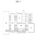
- FIG. 7 is an example diagram illustrating a state in which an LCD device including the LED array driving apparatus according to the second embodiment.
- FIG. 2 is a block diagram illustrating an LCD device according to one embodiment.
- FIG. 3 is a block diagram illustrating an embodiment of an LED array and an LED array driving apparatus which are applied to the LCD device.
- the LCD device includes: a panel 100 having a plurality of pixels formed in a plurality of areas defined by intersections between a plurality of gate lines and a plurality of data lines; a plurality of drivers 200, 300 and 400 that control signals to be supplied to the gate lines and the data lines; an LED array 600 that irradiates light on the panel 100; and an LED array driving apparatus 500 that changes a resistance value according to a selection signal received from an external system 900 to vary the amount of current provided to the LED array 600.
- the external system 900 controls the function of an electronic product using the LCD device according to one embodiment.
- the external system 900 may be a main board that controls a function of the computer, and, when the electronic product is a TV, the external system 900 may be a main board that controls a function of the TV. Also, when the electronic product is a smart phone, the external system 900 may be a main board that controls a function of the smart phone.
- the external system 900 may be electrically connected to the LED array 600 through a connector 800.
- the panel 100 includes the plurality of pixels including a thin film transistor (TFT) and pixel electrodes formed in each of the plurality of areas defined by intersections between the gate lines and the data lines.
- TFT thin film transistor
- the TFT supplies a data voltage, applied from a corresponding data line, to the pixel electrode in response to a scan signal supplied from a corresponding gate line.
- the pixel electrode drives liquid crystal filled between the pixel electrode and a common electrode to adjust a transmittance of light in response to the data voltage.
- a liquid crystal mode of the panel 100 may use various liquid crystal modes, in addition to a twisted nematic (TN) mode, a vertical alignment (VA) mode, an in-plane switching (IPS) mode, and a fringe field switching (FFS) mode.
- the LCD device may be implemented in various types such as a transmissive LCD device, a semi-transmissive LCD device, a reflective LCD device, etc.
- the driver controls signals to be supplied to the gate lines and the data lines, and includes a gate driving IC 200 for supplying the scan signal to the gate lines, a source driving IC 300 for supplying data voltages to the respective data lines, and a timing controller 400 for controlling the gate driving IC 200 and the source driving IC 300.
- the timing controller 400 generates a gate control signal GCS for controlling an operation timing of each of the gate driving ICs (GDIC#1 through GDIC#4) 200 and a data control signal DCS for controlling an operation timing of each of the source driving ICs (SDIC#1 through SDIC#6) 300 by using a timing signal (e.g., a vertical sync signal Hsync, a horizontal sync signal Hsync, a data enable signal DE, etc.) received from the external system 900.
- a timing signal e.g., a vertical sync signal Hsync, a horizontal sync signal Hsync, a data enable signal DE, etc.
- the gate control signal GCS includes a gate start pulse GSP, a gate shift clock signal GCS, a gate output enable signal GOE, a gate start signal VST, etc.
- the data control signal DCS includes a source start pulse SSP, a source sampling clock SSC, a source output enable signal SOE, a polarity control signal POL, etc.
- the timing controller 400 realigns digital input video data (input RGB) received from the external system 900 according to a pixel type of the panel 100, and supplies the realigned image data to the source driving ICs 300.
- Each of the gate driving ICs (GDIC#1 through GDIC#4) 200 supplies the scan signal to the gate lines by using the gate control signal GCS generated by the timing controller 400.
- the gate driving IC 200 may use the same or similar gate driving IC used in the LCD device of FIG. 1 .
- the gate driving IC 200 as illustrated in FIG. 3 may be configured independently from the panel 100, and electrically connected to the panel 100 in various ways.
- the gate driving IC 200 may be a gate-in-panel (GIP) type where the gate driving IC 200 is disposed in the panel 100.
- GIP gate-in-panel
- Each of the source driving IC 300 converts digital image data transferred from the timing controller 400 into data voltages, and supplies the data voltages of horizontal lines to the corresponding data lines at every horizontal period. For each horizontal period, a scan signal is supplied to one gate line.
- the source driving IC 300 converts the image data into the data voltages by using gamma voltages supplied from a gamma voltage generator (not shown), and outputs the data voltages to the corresponding data lines.
- the source driving IC 300 includes a shift register, a latch, a digital-to-analog converter (DAC), and an output buffer.
- the shift register generates a sampling signal by using data control signals (SSC, SSP, etc.) received from the timing controller 400.
- the latch latches the digital image data sequentially received from the timing controller 400, and then simultaneously outputs the latched image data to the DAC.
- the DAC simultaneously converts the image data, transferred from the latch, into positive or negative data voltages, and outputs the positive or negative data voltages. Specifically, the DAC converts the image data into the positive or negative data voltages by using a polarity control signal POL received from the timing controller 400, and outputs the positive or negative data voltages to the corresponding data lines. The DAC converts the image data into the respective data voltages by using a high-level driving voltage VDD.
- the output buffer outputs the positive or negative data voltages, transferred from the DAC, to the corresponding data lines of the panel 100 according to a source output enable signal SOE received from the timing controller 400.
- the source driving IC 300 may receive image data from the timing controller 400 by using an embedded point to point interface (EPI) type interface, or receive image data from the timing controller 400 by using mini-low voltage differential signaling (LVDS) type interface.
- EPI embedded point to point interface
- LVDS mini-low voltage differential signaling
- the LED array 600 may include N number of LED strings 620.
- Each of the N LED strings 620 includes a plurality of LEDs 610 which are serially connected to each other.
- the LED array driving apparatus 500 changes a resistance value according to the selection signal inputted from the external system 900 to vary the amount of current sent to the LED array 600.
- Power consumed by the LED array 600 varies according to the amount of current supplied to the LED array 600.
- power consumption of the LED array is controlled by controlling a time during which the current flows to the LED array, according to a PWM signal. Accordingly, the power consumption of the LED array 600 may vary according to a pulse width of the PWM signal.
- the LED array driving apparatus 500 varies the amount of current supplied to the LED array 600. That is, in the related art, an amount of current supplied to the LED array 600 is set to the maximum value which enables the LED array 600 to output the maximum luminance. An amount of current supplied to the LED array 600 is set to a specific value by a user's selection.
- Embodiments detect a level of voltage at node or current in the node connected to a controller to set a current in the LED array to a specific value.
- a level of the driving current may vary according to a resistance value of the LED array driving apparatus 500.
- the LED array driving apparatus 500 includes: a current amount setter 520 that has a resistance value varying according to the selection signal inputted from the external system 900; and a controller 510 that generates a driving voltage and a driving current by using the input voltage VIN received from the external system 900 and a level of voltage at a node 544 or the current in the node 544 of the current amount setter 520, and supplies the driving voltage and the driving current to the LED array 600. That is, the level of the driving current supplied to the LED array 600 may vary by changing the resistance value of the current amount setter 520.
- a current of 42.9 mA is supplied from the controller 510 to the LED array 600, and thus a luminance of the LED array 600 is 100%.
- a current of 28.6 mA is supplied from the controller 510 to the LED array 600, and thus the luminance of the LED array 600 is changed to 75%
- a current of 21.4 mA is supplied from the controller 510 to the LED array 600, and thus the luminance of the LED array 600 is changed to 50%.
- the current amount setter 520 includes at least one or more selection terminals for receiving the selection signal from the external system 900. A specific example of the current amount setter 520 will be described in detail with reference to FIGS. 4 through 7 .
- the LED array driving apparatus 500 as illustrated in FIG. 2 , is mounted on a main board 700, and connected to the external system 900 through the connector 800.
- the timing controller 400 may be mounted on the main board 700. That is, the LED array driving apparatus 500 and the timing controller 400 are mounted on the main board 700, and electrically connected to the external system 900 through the connector 800. The input video data and the timing signals may be transferred from the external system 900 to the timing controller 400 through the connector 800.
- the LED array driving apparatus 500 may further include a current amount selector 530 configured with a plurality of switching transistors 531 which are connected between a ground terminal and the corresponding LED strings 620 of the LED array 600.
- a direct current (DC) signal from the external system 900 is supplied to the switching transistors 531.
- the DC signal remains constant throughout a frame cycle of the LCD device.
- the switching transistors 531 maintain a turn-on state, and thus, the amount of current flowing to the LED array 600 remains substantially unchanged during the frame cycle. Therefore, a certain current selected according to a resistance value set by the current amount setter 520 may be continuously supplied to the LED array 600.
- the controller 500 may include a power supplier 511 operating as a variable current source for the LED strings 620 and a DC signal supplier 512 that transfers the DC signal received from the external system 900 to the switching transistors 531.
- the power supplier 511 generates current outputs for LED strings 620 based on the input voltage VIN received from the external system 900 and the resistance value set by the current amount setter 520, and supplies the current to the LED strings of the LED array 600.
- the DC signal supplier 512 supplies the DC signal received from the external system 900 to the switching transistors 531.
- the switching transistors 531 configuring the current amount selector 530 may be provided inside the controller 510.
- the controller 510 is implemented as MAX 16814 integrated circuit, available from Maxim Integrated at San Jose, California.
- the related art LED array driving apparatus of FIG. 1 includes the switching unit 53 instead of the current amount selector 530, and includes the current amount controller 51b instead of the DC signal supplier 512.
- a PWM signal is sent to the current amount controller 51b, and then sent to the switching transistors of the switching unit 53.
- the DC signal is sent to the DC signal supplier 512 included in the LED array driving apparatus, and then sent to the switching transistors of the current amount selector 530.
- FIG. 4 is a block diagram illustrating an embodiment of a current amount setter applied to an LED array driving apparatus according to a first embodiment
- FIG. 5 is an exemplary diagram illustrating a state in which an LCD device including the LED array driving apparatus according to the first embodiment is connected to the external system through a connector
- FIG. 6 is a block diagram illustrating an embodiment of a current amount setter applied to an LED array driving apparatus according to a second embodiment
- FIG. 7 is an exemplary diagram illustrating a state in which an LCD device including the LED array driving apparatus according to the second embodiment is connected to the external system through a connector.
- the current amount setter 520 may include a selection terminal A connected to a selection signal terminal A' of the external system through the connector 800, a transistor Q1 having a gate terminal connected to the selection terminal A, a plurality of resistors R1 to R3 connected to the transistor Q1 in serial or parallel, and a diode D1 connected to the transistor Q1.
- the current amount setter 520 is connected to the power supplier 511 of the controller 510.
- the voltage at node 633 or current in node 633 of the current amount setter 520 is changed.
- Such change in the voltage or current in node 633 is detected by the power supplier 511 and causes the amount of current generated by the power supplier 511 to be changed accordingly.
- the arrangement and number of the transistor, resistors, and diode included in the current amount setter 520 may be varied depending on a range of a current to be varied.
- the selection terminal A may be connected to a high-level voltage terminal or a ground terminal through the selection signal terminal A' of the external system, or may be maintained in a high impedance state (i.e., an open circuit state where the selection terminal is not connected to any output of the external system).
- a total resistance value of the current amount setter 520 may be changed according to the selection terminal A being connected to the high-level voltage terminal or ground terminal or having the open state. That is, one selection terminal A connected to the external system 900 is provided in the current amount setter 520, and the current amount setter 520 has different resistance values according to the selection terminal A being connected to the high-level voltage terminal or ground terminal through the external system 900 or being maintained the open state.
- the level of the driving current generated by the controller 510 varies according to the resistance value.
- the LED array driving apparatus 500 according to the first embodiment and the timing controller 400 may be mounted on the main board 700.
- the LED array driving apparatus 500 and the timing controller 400 may be electrically connected to the external system 900 through the connector 800.
- the current amount setter 520 applied to the LED array driving apparatus may include at least two or more selection terminals B and C connected to the selection signal terminal A' of the external system through the connector 800, a plurality of resistors R1 through R3 connected in series with the selection terminals B and C connected to nodes 610, 614 between the resistors R1 through R3, and a capacitor C connected to the resistors R1 through R3 in parallel.
- the current amount setter 520 is connected to the power supplier 511 of the controller 510. When the resistance value of the current amount setter 520 is changed, the voltage at the node 544 or the current in the node 544 is changed. This in turn changes the amount of current generated by the power supplier 511.
- the arrangement and number of the resistors, capacitor, and selection terminals B and C included in the current amount setter 520 may be varied depending on a range of a current.
- the selection terminals B and C may be respectively connected to the ground terminal through respective selection signal terminals B' and C' of the external system, or may be maintained in an open state.
- the total resistance value of the current amount setter 520 may be changed according to the selection terminals B and C being connected to the ground terminal or having the open state. That is, at least two or more selection terminals B and C connected to the ground terminal or maintained in the open state are provided in the current amount setter 520, and the current amount setter 520 has different resistance values according to selection terminals B and C being connected to the ground terminal through the external system 900 or being maintained in the open state.
- the level of the driving current outputted from the controller 510 varies according to the resistance value.
- the LED array driving apparatus 500 according to the second embodiment and the timing controller 400 may be mounted on the main board 700.
- the LED array driving apparatus 500 and the timing controller 400 may be electrically connected to the external system 900 through the connector 800.
- the luminance of the LED array is adjusted even without using a PWM signal, and hence, the need for an additional circuit for generating the PWM signal is obviated.
- the removal of the PWM signal and the circuit for generating this signal also removes a wavy noise caused by the PWM signal.
Landscapes
- Physics & Mathematics (AREA)
- Nonlinear Science (AREA)
- Mathematical Physics (AREA)
- Chemical & Material Sciences (AREA)
- Crystallography & Structural Chemistry (AREA)
- General Physics & Mathematics (AREA)
- Optics & Photonics (AREA)
- Control Of Indicators Other Than Cathode Ray Tubes (AREA)
- Liquid Crystal (AREA)
Abstract
Description
- This application claims the benefit of the Korean Patent Application No.
10-2012-0148659 filed on December 18, 2012 - The disclosure relate to an apparatus for driving a light emitting diode (LED) array, and more particularly, to an apparatus for driving an LED array used as a backlight of a liquid crystal display (LCD) device and an LCD device using the same.
- Flat panel display devices are widely used for various electronic devices such as large-size digital televisions (TVs) requiring a reduction in weight and thickness as well as mobile devices which necessarily need a small size and low power. In the flat panel display devices, LCD devices are applied to all electronic products ranging from small-size devices to large-size devices, and thus are being most widely used.
- Since a liquid crystal panel applied to LCD devices cannot self-illuminate, a light source called a backlight is disposed at a rear surface of the liquid crystal panel. Light emitted from the backlight is outputted to the outside through a liquid crystal layer and color filter of the liquid crystal panel, thereby enabling an image to be displayed by the liquid crystal panel. Cold cathode fluorescent lamps (CCFLs), external electrode fluorescent lamps (EEFLs), or the like are being widely used as the backlight.
- However, recently, LEDs which are sufficiently high in luminance and are low in power consumption and manufacturing cost were developed to replace the above-described backlights. That is, since a backlight unit using an LED array does not use a high-cost diffusive film and does not need an inverter unlike fluorescent lamps, the manufacturing cost can be saved, a panel can be easily enlarged in size, a thickness and weight can be reduced, and power consumption and environmental problems can decrease. Accordingly, the backlight unit using the LED array is being widely used.
- A backlight unit using LEDs includes an LED array having a plurality of LED strings, each of which is configured with a plurality of LEDs. An amount of light emitted from an LED is proportional to a level of a driving current passing through an active layer of the LED. Driving of the LED denotes supplying and controlling a driving current which flows to the LED.
-
FIG. 1 is an exemple diagram illustrating a configuration of a related art apparatus for driving anLED array 60. Arelated art apparatus 50 for driving anLED array 60, as illustrated inFIG. 1 , includes: acontrol unit 51 that supplies power to anLED array 60 by using an input voltage VIN received from an external source, and controls the amount of current to flow in theLED array 60; acurrent fixing unit 52 that provides a certain resistance to thecontrol unit 51 in order for a certain amount of current to be supplied to theLED array 60; and a switching unit 53 that controls current flowing in theLED array 60 to vary a luminance of theLED array 60. - The
control unit 51 is generally configured as an integrated circuit (IC), and may be mounted on a main board of an LCD device together with a timing controller. The switching unit (current varying unit) 53 may be provided inside or outside thecontrol unit 51. Thecurrent fixing unit 52 is disposed outside thecontrol unit 51, and set to have a certain resistance value. - The
related art apparatus 50 for driving the LED array controls the luminance of theLED array 60, for controlling the power consumption of theLED array 60. To this end, first, thecurrent fixing unit 52 is set to have an impedance value, which controls the maximum current supplied to theLED array 60 and thus enables theLED array 60 to output a luminance of 100%. Therefore, thecontrol unit 51 continuously supplies a current having the maximum value to theLED array 60 by using the resistance value set by thecurrent fixing unit 52 and the input voltage VIN supplied from an external system. - The
control unit 51 includes apower supplier 51a for supplying a voltage and a current to theLED array 60 by using the input voltage VIN and the maximum current. A current supplied to theLED array 60 is fixed to the maximum value by thecurrent fixing unit 52, and theLED array 60 outputs the maximum luminance with the maximum current. - When the
LED array 60 outputs light having the maximum luminance, an image displayed by a panel can be preferably sharpened. However, when theLED array 60 outputs light having the maximum luminance, energy consumption increases proportionally. In order to decrease the amount of consumed energy, thecontrol unit 51 generally uses a pulse width modulation (PWM) signal received from the external system. For this purpose, thecontrol unit 51 includes acurrent amount controller 51b. - The PWM signal is composed of pulses that have a constant cycle but vary in pulse width, and a turn-on time of a thin film transistor (TFT) configuring the switching unit 53 is controlled by the PWM signal. The time during which the maximum current flows to the
LED array 60 is controlled by controlling the turn-on time of the TFT, and thus, a luminance of theLED array 60 may be changed. For example, in dividing one pulse width by a cycle ratio, a high signal occupies 10% and a low signal occupies 90% when a ratio of 10%, and when a ratio of 70%, the high signal occupies 70% and the low signal occupies 30%. - Specifically, when the PWM signal is generated at the ratio of 10%, a high signal having a narrow pulse width is generated, and inputted to the switching unit 53 through the
current amount controller 51b. In this case, since the pulse width of the high signal is narrow, a time for which the TFT of the switching unit 53 is turned on is shortened, and thus, a time for which a current flows to theLED array 60 is shortened. Therefore, the luminance of theLED array 60 decreases. - On the other hand, when the PWM signal is generated at the ratio of 70%, a high signal having a broad pulse width is generated, and inputted to the switching unit 53 through the
current amount controller 51b. In this case, since the pulse width of the high signal is broad, a time for which the TFT of the switching unit 53 is turned on is extended, and thus, a time for which a current flows to theLED array 60 is extended. Therefore, the luminance of theLED array 60 increases. - Manufacturers of various electronic products such as notebook computers, TVs, tablet personal computers (PCs), etc., by using the above-described LCD device, may adjust the amplitude of the pulse width of the PWM signal sent to the
control unit 51 to adjust the amount of power consumed by the LCD device and electronic product. - In order to drive the LCD device and an electronic product with low power, a PWM signal having a narrow pulse width may be received at the current
amount control unit 51b from the external system. Conversely, in order to drive the LCD device and an electronic product with high power so as to display a clear image, a PWM signal having a broad pulse width may be received at the currentamount control unit 51b from the external system. Accordingly, electronic products vary the pulse width of the PWM signal, and thus drive the LCD devices with desired power. - However, the above-described LCD device of the related art has the following problems. First, the PWM signal must be received from the external system to the
control unit 51, for adjusting the luminance of theLED array 60. Therefore, it is difficult for a manufacturer, which is unable to directly develop a PWM signal, to manufacture an electronic product by using the related art LCD device. - Second, the PWM signal for adjusting the luminance of the
LED array 60 is required to be synchronized with the frame rate of the LCD device so as to prevent a wavy noise. Therefore, the external system which is driven in connection with the related art LCD device needs to include separate circuits for generating the PWM signal synchronized with the frame rate. For this reason, there is a limitation in developing and manufacturing the external system. - Embodiments relate to an apparatus for driving a light emitting diode (LED) array. The apparatus includes a current amount setter and a controller coupled to the current amount setter and the LED array. The current amount setter varies a voltage at a node or a current in the node of the current amount setter according to a selection signal from an external system. The controller includes a power supplier and a signal supplier. The power supplier adjusts a level of current provided to the LED array based on an input voltage received from the external system and the resistance across the current amount setter. The signal supplier distributes direct current (DC) signals remaining unchanged during a frame cycle to a plurality of switches coupled to the LED array to turn on or off LEDs in the LED array.
- Various embodiments provide an apparatus for driving a light emitting diode (LED), the apparatus comprising: a current amount setter configured to vary a voltage at a node or a current in the node of the current amount setter according to a selection signal from an external system; and a controller coupled to the current amount setter and the LED array, the controller comprising: a power supplier connected to the node of the current amount setter and configured to adjust a level of current provided to the LED array based on an input voltage received from the external system and the voltage at the node or the current in the node of the current amount setter, and a signal supplier configured to distribute direct current (DC) signals remaining unchanged during a frame cycle to a plurality of switches coupled to the LED array to turn on or off LEDs in the LED array.
- In one or more embodiments, the power supplier is configured to adjust the level of current provided to the LED array based on the input voltage received from the external system and a resistance across the current amount setter.
- In one or more embodiments, the current amount setter comprises a selection terminal connected to the external system, a resistance across the current amount setter determined based on connection of the selection terminal to a high-level voltage terminal or a ground terminal through the external system or being maintained in a high impedance state.
- In one or more embodiments, the current amount setter comprises a capacitor between the node and a low reference voltage; a transistor having a gate coupled to the selection terminal; a diode between a source of the transistor and the selection terminal; a first resistor between the source of the transistor and the node; a second resistor between the source of the transistor and the low reference voltage; and a third resistor between a drain of the transistor and the low reference voltage.
- In one or more embodiments, the current amount setter comprises at least two selection terminals connected to a ground terminal or maintained in an high impedance state, a resistance across the current amount setter determined based on connection of the selection terminals to the ground terminal through the external system or being maintained in a high impedance state.
- In one or more embodiments, the current amount setter comprises a string of resistors connected in parallel to a capacitor, each of the at least two selection terminals connected between the string of resistors.
- In one or more embodiments, the plurality of switches are configured as switching transistors and are connected between a ground terminal and a plurality of LED strings in the LED array.
- In one or more embodiments, the signal supplier is configured to distribute the DC signals to the plurality of switches responsive to receiving a DC signal from the external system.
- In one or more embodiments, the LED array comprises a plurality of strings of LEDs, each string of LEDs coupled to a low reference voltage via each of the plurality of switches.
- Various embodiments provide a liquid crystal display (LCD) device including an apparatus for driving a light emitting diode (LED) array, the LCD device comprising: a panel in which a plurality of pixels are respectively formed in a plurality of areas defined by intersections between a plurality of gate lines and a plurality of data lines, the panel irradiated by light from the LED array; a driver configured to control signals to be supplied to the gate lines and the data lines; and an LED array driving apparatus according to any one of the embodiments described herein.
- Various embodiments provide a liquid crystal display (LCD) device including an apparatus for driving a light emitting diode (LED) array, the LCD device comprising: a panel in which a plurality of pixels are respectively formed in a plurality of areas defined by intersections between a plurality of gate lines and a plurality of data lines, the panel irradiated by light from the LED array; a driver configured to control signals to be supplied to the gate lines and the data lines; and an LED array driving apparatus comprising: a current amount setter configured to vary a voltage at a node or a current in the node of the current amount setter according to a selection signal from an external system; and a controller coupled to the current amount setter and the LED array, the controller comprising: a power supplier configured to adjust a level of current provided to the LED array based on an input voltage received from the external system and the resistance across the current amount setter, and a signal supplier configured to distribute direct current (DC) signals remaining unchanged during a frame cycle to a plurality of switches coupled to the LED array to turn on or off LEDs in the LED array.
- In one or more embodiments, the current amount setter comprises a selection terminal connected to the external system, a resistance across the current amount setter determined based on connection of the selection terminal to a high-level voltage terminal or a ground terminal through the external system or being maintained in a high impedance state.
- In one or more embodiments, the current amount setter comprises a capacitor between the node and a low reference voltage; a transistor having a gate coupled to the selection terminal; a diode between a source of the transistor and the selection terminal; a first resistor between the source of the transistor and the node; a second resistor between the source of the transistor and the low reference voltage; and a third resistor between a drain of the transistor and the low reference voltage.
- In one or more embodiments, the current amount setter comprises at least two selection terminals connected to a ground terminal or maintained in an high impedance state, the resistance across the current amount setter determined based on connection of the selection terminals to the ground terminal through the external system or being maintained in a high impedance state.
- In one or more embodiments, the current amount setter comprises a string of resistors connected in parallel to a capacitor, each of the at least two selection terminals connected to a node between the string of resistors.
- In one or more embodiments, the plurality of switching transistors are connected between a ground terminal and a plurality of LED strings in the LED array.
- In one or more embodiments, the signal supplier is configured to distribute the DC signals to the plurality of switches responsive to receiving a DC signal from the external system.
- In one or more embodiments, the LED array comprises a plurality strings of LEDs, each string of LEDs coupled to a low reference voltage via each of the plurality of switches.
- The accompanying drawings, which are included to provide a further understanding of the invention and are incorporated in and constitute a part of this application, illustrate embodiments of the invention and together with the description serve to explain the principle of the invention. In the drawings:
-
FIG. 1 is an example diagram illustrating a configuration of a related art apparatus for driving an LED array; -
FIG. 2 is a block diagram illustrating an embodiment of an LCD device according to one embodiment; -
FIG. 3 is a block diagram illustrating an embodiment of an LED array and an LED array driving apparatus which are applied to the LCD device according to one embodiment; -
FIG. 4 is a block diagram illustrating an embodiment of a current amount setter applied to an LED array driving apparatus according to a first embodiment; -
FIG. 5 is an example diagram illustrating a state in which an LCD device including the LED array driving apparatus according to the first embodiment; -
FIG. 6 is a block diagram illustrating an embodiment of a current amount setter applied to an LED array driving apparatus according to a second embodiment; and -
FIG. 7 is an example diagram illustrating a state in which an LCD device including the LED array driving apparatus according to the second embodiment. - Reference will now be made in detail to the exemplary embodiments, examples of which are illustrated in the accompanying drawings. Wherever possible, the same reference numbers will be used throughout the drawings to refer to the same or like parts.
- Hereinafter, embodiments will be described in detail with reference to the accompanying drawings.
-
FIG. 2 is a block diagram illustrating an LCD device according to one embodiment.FIG. 3 is a block diagram illustrating an embodiment of an LED array and an LED array driving apparatus which are applied to the LCD device. - The LCD device, as illustrated in
FIG. 2 , includes: apanel 100 having a plurality of pixels formed in a plurality of areas defined by intersections between a plurality of gate lines and a plurality of data lines; a plurality ofdrivers LED array 600 that irradiates light on thepanel 100; and an LEDarray driving apparatus 500 that changes a resistance value according to a selection signal received from anexternal system 900 to vary the amount of current provided to theLED array 600. Here, theexternal system 900 controls the function of an electronic product using the LCD device according to one embodiment. For example, when the electronic product is a computer, theexternal system 900 may be a main board that controls a function of the computer, and, when the electronic product is a TV, theexternal system 900 may be a main board that controls a function of the TV. Also, when the electronic product is a smart phone, theexternal system 900 may be a main board that controls a function of the smart phone. Theexternal system 900 may be electrically connected to theLED array 600 through aconnector 800. - The
panel 100 includes the plurality of pixels including a thin film transistor (TFT) and pixel electrodes formed in each of the plurality of areas defined by intersections between the gate lines and the data lines. - The TFT supplies a data voltage, applied from a corresponding data line, to the pixel electrode in response to a scan signal supplied from a corresponding gate line. The pixel electrode drives liquid crystal filled between the pixel electrode and a common electrode to adjust a transmittance of light in response to the data voltage.
- A liquid crystal mode of the
panel 100 may use various liquid crystal modes, in addition to a twisted nematic (TN) mode, a vertical alignment (VA) mode, an in-plane switching (IPS) mode, and a fringe field switching (FFS) mode. Also, the LCD device may be implemented in various types such as a transmissive LCD device, a semi-transmissive LCD device, a reflective LCD device, etc. - The driver controls signals to be supplied to the gate lines and the data lines, and includes a
gate driving IC 200 for supplying the scan signal to the gate lines, asource driving IC 300 for supplying data voltages to the respective data lines, and atiming controller 400 for controlling thegate driving IC 200 and thesource driving IC 300. - The
timing controller 400 generates a gate control signal GCS for controlling an operation timing of each of the gate driving ICs (GDIC# 1 through GDIC#4) 200 and a data control signal DCS for controlling an operation timing of each of the source driving ICs (SDIC# 1 through SDIC#6) 300 by using a timing signal (e.g., a vertical sync signal Hsync, a horizontal sync signal Hsync, a data enable signal DE, etc.) received from theexternal system 900. - The gate control signal GCS includes a gate start pulse GSP, a gate shift clock signal GCS, a gate output enable signal GOE, a gate start signal VST, etc. The data control signal DCS includes a source start pulse SSP, a source sampling clock SSC, a source output enable signal SOE, a polarity control signal POL, etc.
- Moreover, the
timing controller 400 realigns digital input video data (input RGB) received from theexternal system 900 according to a pixel type of thepanel 100, and supplies the realigned image data to thesource driving ICs 300. - Each of the gate driving ICs (
GDIC# 1 through GDIC#4) 200 supplies the scan signal to the gate lines by using the gate control signal GCS generated by thetiming controller 400. Thegate driving IC 200 may use the same or similar gate driving IC used in the LCD device ofFIG. 1 . - The
gate driving IC 200 as illustrated inFIG. 3 , may be configured independently from thepanel 100, and electrically connected to thepanel 100 in various ways. Alternatively, thegate driving IC 200 may be a gate-in-panel (GIP) type where thegate driving IC 200 is disposed in thepanel 100. - Each of the
source driving IC 300 converts digital image data transferred from thetiming controller 400 into data voltages, and supplies the data voltages of horizontal lines to the corresponding data lines at every horizontal period. For each horizontal period, a scan signal is supplied to one gate line. - The
source driving IC 300 converts the image data into the data voltages by using gamma voltages supplied from a gamma voltage generator (not shown), and outputs the data voltages to the corresponding data lines. To this end, although not shown, thesource driving IC 300 includes a shift register, a latch, a digital-to-analog converter (DAC), and an output buffer. The shift register generates a sampling signal by using data control signals (SSC, SSP, etc.) received from thetiming controller 400. The latch latches the digital image data sequentially received from thetiming controller 400, and then simultaneously outputs the latched image data to the DAC. The DAC simultaneously converts the image data, transferred from the latch, into positive or negative data voltages, and outputs the positive or negative data voltages. Specifically, the DAC converts the image data into the positive or negative data voltages by using a polarity control signal POL received from thetiming controller 400, and outputs the positive or negative data voltages to the corresponding data lines. The DAC converts the image data into the respective data voltages by using a high-level driving voltage VDD. - The output buffer outputs the positive or negative data voltages, transferred from the DAC, to the corresponding data lines of the
panel 100 according to a source output enable signal SOE received from thetiming controller 400. - The
source driving IC 300 may receive image data from thetiming controller 400 by using an embedded point to point interface (EPI) type interface, or receive image data from thetiming controller 400 by using mini-low voltage differential signaling (LVDS) type interface. - The
LED array 600, as illustrated inFIG. 3 , may include N number of LED strings 620. Each of the N LED strings 620 includes a plurality ofLEDs 610 which are serially connected to each other. - The LED
array driving apparatus 500 changes a resistance value according to the selection signal inputted from theexternal system 900 to vary the amount of current sent to theLED array 600. - Power consumed by the
LED array 600 varies according to the amount of current supplied to theLED array 600. In the related art, when the amount of current supplied to theLED array 600 is fixed to the maximum amount of current, power consumption of the LED array is controlled by controlling a time during which the current flows to the LED array, according to a PWM signal. Accordingly, the power consumption of theLED array 600 may vary according to a pulse width of the PWM signal. - On the other hand, the LED
array driving apparatus 500 according to embodiments varies the amount of current supplied to theLED array 600. That is, in the related art, an amount of current supplied to theLED array 600 is set to the maximum value which enables theLED array 600 to output the maximum luminance. An amount of current supplied to theLED array 600 is set to a specific value by a user's selection. - Embodiments detect a level of voltage at node or current in the node connected to a controller to set a current in the LED array to a specific value. When the LED
array driving apparatus 500 generates a driving current to be supplied to theLED array 600 by using the input voltage VIN supplied from theexternal system 900, a level of the driving current may vary according to a resistance value of the LEDarray driving apparatus 500. - To use the above-described method, as illustrated in
FIG. 3 , the LEDarray driving apparatus 500 according to an embodiment includes: acurrent amount setter 520 that has a resistance value varying according to the selection signal inputted from theexternal system 900; and acontroller 510 that generates a driving voltage and a driving current by using the input voltage VIN received from theexternal system 900 and a level of voltage at anode 544 or the current in thenode 544 of thecurrent amount setter 520, and supplies the driving voltage and the driving current to theLED array 600. That is, the level of the driving current supplied to theLED array 600 may vary by changing the resistance value of thecurrent amount setter 520. - For example, when the total resistance value of the
current amount setter 520 is 35 kΩ, a current of 42.9 mA is supplied from thecontroller 510 to theLED array 600, and thus a luminance of theLED array 600 is 100%. In this state, when the total resistance value of thecurrent amount setter 520 is changed to 52.5 kΩ, a current of 28.6 mA is supplied from thecontroller 510 to theLED array 600, and thus the luminance of theLED array 600 is changed to 75%, and, when the total resistance value of thecurrent amount setter 520 is changed to 70 kΩ, a current of 21.4 mA is supplied from thecontroller 510 to theLED array 600, and thus the luminance of theLED array 600 is changed to 50%. - Therefore, a user desiring to drive the
LED array 600 with the minimum power supplies the selection signal, allowing thenode 544 of thecurrent amount setter 520 to have a voltage or current which allows the driving current to be the minimum, to thecurrent amount setter 520 through theexternal system 900. To this end, thecurrent amount setter 520 includes at least one or more selection terminals for receiving the selection signal from theexternal system 900. A specific example of thecurrent amount setter 520 will be described in detail with reference toFIGS. 4 through 7 . - The LED
array driving apparatus 500, as illustrated inFIG. 2 , is mounted on amain board 700, and connected to theexternal system 900 through theconnector 800. - Among the drivers, especially, the
timing controller 400 may be mounted on themain board 700. That is, the LEDarray driving apparatus 500 and thetiming controller 400 are mounted on themain board 700, and electrically connected to theexternal system 900 through theconnector 800. The input video data and the timing signals may be transferred from theexternal system 900 to thetiming controller 400 through theconnector 800. - The LED
array driving apparatus 500 may further include acurrent amount selector 530 configured with a plurality of switchingtransistors 531 which are connected between a ground terminal and the correspondingLED strings 620 of theLED array 600. A direct current (DC) signal from theexternal system 900 is supplied to the switchingtransistors 531. - The DC signal remains constant throughout a frame cycle of the LCD device. When the DC signal is supplied to the switching
transistors 531, the switchingtransistors 531 maintain a turn-on state, and thus, the amount of current flowing to theLED array 600 remains substantially unchanged during the frame cycle. Therefore, a certain current selected according to a resistance value set by thecurrent amount setter 520 may be continuously supplied to theLED array 600. - In order for the DC signal to be supplied from the
external system 900 to the switchingtransistors 531, thecontroller 500 may include apower supplier 511 operating as a variable current source for the LED strings 620 and aDC signal supplier 512 that transfers the DC signal received from theexternal system 900 to the switchingtransistors 531. - The
power supplier 511 generates current outputs forLED strings 620 based on the input voltage VIN received from theexternal system 900 and the resistance value set by thecurrent amount setter 520, and supplies the current to the LED strings of theLED array 600. - The
DC signal supplier 512 supplies the DC signal received from theexternal system 900 to the switchingtransistors 531. - In other embodiments, the switching
transistors 531 configuring thecurrent amount selector 530 may be provided inside thecontroller 510. - In one embodiment, the
controller 510 is implemented as MAX 16814 integrated circuit, available from Maxim Integrated at San Jose, California. - The related art LED array driving apparatus of
FIG. 1 includes the switching unit 53 instead of thecurrent amount selector 530, and includes thecurrent amount controller 51b instead of theDC signal supplier 512. In the related art LED array driving apparatus ofFIG. 1 , a PWM signal is sent to thecurrent amount controller 51b, and then sent to the switching transistors of the switching unit 53. - However, the DC signal is sent to the
DC signal supplier 512 included in the LED array driving apparatus, and then sent to the switching transistors of thecurrent amount selector 530. -
FIG. 4 is a block diagram illustrating an embodiment of a current amount setter applied to an LED array driving apparatus according to a first embodiment,FIG. 5 is an exemplary diagram illustrating a state in which an LCD device including the LED array driving apparatus according to the first embodiment is connected to the external system through a connector,FIG. 6 is a block diagram illustrating an embodiment of a current amount setter applied to an LED array driving apparatus according to a second embodiment, andFIG. 7 is an exemplary diagram illustrating a state in which an LCD device including the LED array driving apparatus according to the second embodiment is connected to the external system through a connector. - The
current amount setter 520 according to the first embodiment, as illustrated inFIGS. 4 and5 , may include a selection terminal A connected to a selection signal terminal A' of the external system through theconnector 800, a transistor Q1 having a gate terminal connected to the selection terminal A, a plurality of resistors R1 to R3 connected to the transistor Q1 in serial or parallel, and a diode D1 connected to the transistor Q1. Thecurrent amount setter 520 is connected to thepower supplier 511 of thecontroller 510. - When the impedance of the
current amount setter 520 is changed, the voltage atnode 633 or current innode 633 of thecurrent amount setter 520 is changed. Such change in the voltage or current innode 633 is detected by thepower supplier 511 and causes the amount of current generated by thepower supplier 511 to be changed accordingly. The arrangement and number of the transistor, resistors, and diode included in thecurrent amount setter 520 may be varied depending on a range of a current to be varied. - In this case, the selection terminal A may be connected to a high-level voltage terminal or a ground terminal through the selection signal terminal A' of the external system, or may be maintained in a high impedance state (i.e., an open circuit state where the selection terminal is not connected to any output of the external system).
- A total resistance value of the
current amount setter 520 may be changed according to the selection terminal A being connected to the high-level voltage terminal or ground terminal or having the open state. That is, one selection terminal A connected to theexternal system 900 is provided in thecurrent amount setter 520, and thecurrent amount setter 520 has different resistance values according to the selection terminal A being connected to the high-level voltage terminal or ground terminal through theexternal system 900 or being maintained the open state. The level of the driving current generated by thecontroller 510 varies according to the resistance value. - The LED
array driving apparatus 500 according to the first embodiment and thetiming controller 400 may be mounted on themain board 700. In this case, as illustrated inFIG. 5 , the LEDarray driving apparatus 500 and thetiming controller 400 may be electrically connected to theexternal system 900 through theconnector 800. - The
current amount setter 520 applied to the LED array driving apparatus according to the second embodiment, as illustrated inFIGS. 6 and7 , may include at least two or more selection terminals B and C connected to the selection signal terminal A' of the external system through theconnector 800, a plurality of resistors R1 through R3 connected in series with the selection terminals B and C connected tonodes current amount setter 520 is connected to thepower supplier 511 of thecontroller 510. When the resistance value of thecurrent amount setter 520 is changed, the voltage at thenode 544 or the current in thenode 544 is changed. This in turn changes the amount of current generated by thepower supplier 511. - The arrangement and number of the resistors, capacitor, and selection terminals B and C included in the
current amount setter 520 may be varied depending on a range of a current. - In this case, the selection terminals B and C may be respectively connected to the ground terminal through respective selection signal terminals B' and C' of the external system, or may be maintained in an open state.
- The total resistance value of the
current amount setter 520 may be changed according to the selection terminals B and C being connected to the ground terminal or having the open state. That is, at least two or more selection terminals B and C connected to the ground terminal or maintained in the open state are provided in thecurrent amount setter 520, and thecurrent amount setter 520 has different resistance values according to selection terminals B and C being connected to the ground terminal through theexternal system 900 or being maintained in the open state. The level of the driving current outputted from thecontroller 510 varies according to the resistance value. - The LED
array driving apparatus 500 according to the second embodiment and thetiming controller 400 may be mounted on themain board 700. In this case, as illustrated inFIG. 7 , the LEDarray driving apparatus 500 and thetiming controller 400 may be electrically connected to theexternal system 900 through theconnector 800. - According to one embodiment, the luminance of the LED array is adjusted even without using a PWM signal, and hence, the need for an additional circuit for generating the PWM signal is obviated. The removal of the PWM signal and the circuit for generating this signal also removes a wavy noise caused by the PWM signal.
- It will be apparent to those skilled in the art that various modifications and variations can be made to embodiments without departing from the spirit or scope of the embodiments.
Claims (10)
- An apparatus for driving a light emitting diode (LED) array, comprising:a current amount setter configured to vary a voltage at a node or a current in the node of the current amount setter according to a selection signal from an external system; anda controller coupled to the current amount setter and the LED array, the controller comprising:a power supplier connected to the node of the current amount setter and configured to adjust a level of current provided to the LED array based on an input voltage received from the external system and the voltage at the node or the current in the node of the current amount setter, anda signal supplier configured to distribute direct current (DC) signals remaining unchanged during a frame cycle to a plurality of switches coupled to the LED array to turn on or off LEDs in the LED array.
- The apparatus of claim 1, wherein the power supplier is configured to adjust the level of current provided to the LED array based on the input voltage received from the external system and a resistance across the current amount setter.
- The apparatus of claim 1 or 2, wherein the current amount setter comprises a selection terminal connected to the external system, a resistance across the current amount setter determined based on connection of the selection terminal to a high-level voltage terminal or a ground terminal through the external system or being maintained in a high impedance state.
- The apparatus of any one of claims 1 to 3, wherein the current amount setter comprises
a capacitor between the node and a low reference voltage;
a transistor having a gate coupled to the selection terminal;
a diode between a source of the transistor and the selection terminal;
a first resistor between the source of the transistor and the node;
a second resistor between the source of the transistor and the low reference voltage; and
a third resistor between a drain of the transistor and the low reference voltage. - The apparatus of claim 1 or 2, wherein the current amount setter comprises at least two selection terminals connected to a ground terminal or maintained in an high impedance state, a resistance across the current amount setter determined based on connection of the selection terminals to the ground terminal through the external system or being maintained in a high impedance state.
- The apparatus of claim 5, wherein the current amount setter comprises a string of resistors connected in parallel to a capacitor, each of the at least two selection terminals connected between the string of resistors.
- The apparatus of any one of claims 1 to 6, wherein the plurality of switches are configured as switching transistors and are connected between a ground terminal and a plurality of LED strings in the LED array.
- The apparatus of any one of claims 1 to 7, wherein the signal supplier is configured to distribute the DC signals to the plurality of switches responsive to receiving a DC signal from the external system.
- The apparatus of any one of claims 1 to 6, wherein the LED array comprises a plurality of strings of LEDs, each string of LEDs coupled to a low reference voltage via each of the plurality of switches.
- A liquid crystal display (LCD) device including an apparatus for driving a light emitting diode (LED) array, the LCD device comprising:a panel in which a plurality of pixels are respectively formed in a plurality of areas defined by intersections between a plurality of gate lines and a plurality of data lines, the panel irradiated by light from the LED array;a driver configured to control signals to be supplied to the gate lines and the data lines; andan LED array driving apparatus according to any one of claims 1 to 9.
Applications Claiming Priority (1)
| Application Number | Priority Date | Filing Date | Title |
|---|---|---|---|
| KR1020120148659A KR102091197B1 (en) | 2012-12-18 | 2012-12-18 | Apparatus for driving a light emitting diode array and liquid crystal display device using the same |
Publications (2)
| Publication Number | Publication Date |
|---|---|
| EP2747518A1 true EP2747518A1 (en) | 2014-06-25 |
| EP2747518B1 EP2747518B1 (en) | 2019-08-14 |
Family
ID=49596194
Family Applications (1)
| Application Number | Title | Priority Date | Filing Date |
|---|---|---|---|
| EP13193774.0A Active EP2747518B1 (en) | 2012-12-18 | 2013-11-21 | Apparatus for driving light emitting diode array and liquid crystal display device using the same |
Country Status (4)
| Country | Link |
|---|---|
| US (1) | US8970472B2 (en) |
| EP (1) | EP2747518B1 (en) |
| KR (1) | KR102091197B1 (en) |
| CN (1) | CN103871372B (en) |
Families Citing this family (8)
| Publication number | Priority date | Publication date | Assignee | Title |
|---|---|---|---|---|
| CN104347047B (en) * | 2014-11-11 | 2016-09-07 | 深圳市华星光电技术有限公司 | Array base palte, display device and driving method thereof |
| US10291998B2 (en) | 2017-01-06 | 2019-05-14 | Nokia Technologies Oy | Discovery, announcement and assignment of position tracks |
| CN109036328B (en) | 2017-06-09 | 2021-09-03 | 京东方科技集团股份有限公司 | Register value transmission method and assembly and display device |
| DE102018111976B3 (en) * | 2018-05-18 | 2019-09-26 | Infineon Technologies Ag | Light-emitting diode driver, light-emitting diode module and corresponding system |
| US11837848B2 (en) * | 2019-09-30 | 2023-12-05 | Analog Modules, Inc. | High PRF, high efficiency laser diode driver power supply |
| DE102019128943B4 (en) * | 2019-10-28 | 2023-07-27 | Insta Gmbh | Arrangement comprising a power supply module and an LED lamp module |
| CN112331135B (en) | 2020-11-05 | 2021-09-24 | Tcl华星光电技术有限公司 | Display panel and driving method |
| KR102382016B1 (en) * | 2021-11-02 | 2022-04-04 | 주식회사 웰랑 | Led driving device providing high led utilization and lighting apparatus including the same |
Citations (1)
| Publication number | Priority date | Publication date | Assignee | Title |
|---|---|---|---|---|
| US20100289424A1 (en) * | 2008-11-17 | 2010-11-18 | Lepower Semiconductor Inc. | Methods and Circuits for LED Drivers and for PWM Dimming Controls |
Family Cites Families (14)
| Publication number | Priority date | Publication date | Assignee | Title |
|---|---|---|---|---|
| JP3272209B2 (en) * | 1995-09-07 | 2002-04-08 | アルプス電気株式会社 | LCD drive circuit |
| JP2000214825A (en) * | 1999-01-20 | 2000-08-04 | Nec Corp | Backlight display device and method |
| JP4984341B2 (en) * | 1999-08-04 | 2012-07-25 | 株式会社デンソー | Display device |
| TWI245250B (en) * | 2003-02-06 | 2005-12-11 | Nec Electronics Corp | Current-drive circuit and apparatus for display panel |
| CN1627132A (en) * | 2003-12-12 | 2005-06-15 | 乐金电子(天津)电器有限公司 | Display unit and method for adjusting brightness |
| US7697583B2 (en) * | 2005-03-30 | 2010-04-13 | Pioneer Corporation | Semiconductor laser driving device and semiconductor laser driving method |
| JP4762681B2 (en) * | 2005-11-07 | 2011-08-31 | ローム株式会社 | LED driver and display device using the same |
| KR20070099942A (en) * | 2006-04-06 | 2007-10-10 | 삼성전자주식회사 | LCD Display |
| KR101362567B1 (en) * | 2008-01-04 | 2014-02-13 | 엘지전자 주식회사 | Dimming control device and light emitting diode lighting system using the same |
| KR101471157B1 (en) * | 2008-06-02 | 2014-12-10 | 삼성디스플레이 주식회사 | A method of driving an emission block, a backlight assembly for performing the same, and a display device having the same |
| JP2010063332A (en) * | 2008-09-08 | 2010-03-18 | Panasonic Corp | Load driving device |
| JP5268615B2 (en) * | 2008-12-15 | 2013-08-21 | キヤノン株式会社 | Power supply device and image forming apparatus |
| TWI508624B (en) * | 2010-09-01 | 2015-11-11 | Au Optronics Corp | Light emitting diode driving method |
| US8742695B2 (en) * | 2012-05-14 | 2014-06-03 | Usai, Llc | Lighting control system and method |
-
2012
- 2012-12-18 KR KR1020120148659A patent/KR102091197B1/en active Active
-
2013
- 2013-10-12 CN CN201310475683.1A patent/CN103871372B/en active Active
- 2013-10-24 US US14/062,541 patent/US8970472B2/en active Active
- 2013-11-21 EP EP13193774.0A patent/EP2747518B1/en active Active
Patent Citations (1)
| Publication number | Priority date | Publication date | Assignee | Title |
|---|---|---|---|---|
| US20100289424A1 (en) * | 2008-11-17 | 2010-11-18 | Lepower Semiconductor Inc. | Methods and Circuits for LED Drivers and for PWM Dimming Controls |
Also Published As
| Publication number | Publication date |
|---|---|
| KR102091197B1 (en) | 2020-03-18 |
| KR20140079084A (en) | 2014-06-26 |
| US20140168569A1 (en) | 2014-06-19 |
| US8970472B2 (en) | 2015-03-03 |
| CN103871372B (en) | 2016-03-30 |
| CN103871372A (en) | 2014-06-18 |
| EP2747518B1 (en) | 2019-08-14 |
Similar Documents
| Publication | Publication Date | Title |
|---|---|---|
| US8970472B2 (en) | Apparatus for driving light emitting diode array and liquid crystal display device using the same | |
| EP3151086B1 (en) | Touch driving signal generating device, touch driving device including the same, and display device and driving method thereof | |
| EP3038096B1 (en) | Liquid crystal display and driving method thereof | |
| CN107808644B (en) | Power supply unit and display device including the same | |
| US9607560B2 (en) | Liquid crystal display device and method for driving the same | |
| KR101281926B1 (en) | Liquid crystal display device | |
| US9548723B1 (en) | Current mode DVR or PVCOM with integrated impedances | |
| CN104424903B (en) | Voltage calibration circuit and liquid crystal display device thereof | |
| KR102278804B1 (en) | Power supply circuit and liquid crystal display comprising the same | |
| CN103187032A (en) | Display device and brightness control method capable of reducing power consumption of display device | |
| KR102113986B1 (en) | Gate driver and display device comprising the same | |
| US8441431B2 (en) | Backlight unit and liquid crystal display using the same | |
| KR102332278B1 (en) | Liquid Crystal Display Device and Driving Method thereof | |
| KR101705366B1 (en) | Back Light Unit and Liquid Crystal Display Device Using the same | |
| CN102110422A (en) | Liquid crystal display and method for compensating color temperature | |
| CN106875903B (en) | Display device and driving method thereof | |
| KR102071952B1 (en) | Liquid crystal display and voltage drop limitation method thereof | |
| KR101213858B1 (en) | Driving circuit and driving method | |
| KR20070053887A (en) | LCD Display | |
| KR102108330B1 (en) | Electronic device including liquid crystal display device and method of driving the same | |
| KR101035988B1 (en) | Display device | |
| US20050200621A1 (en) | Power supply device of LCD module, LCD module of regulating working voltage and method of regulating power supply of LCD module | |
| KR20070063737A (en) | Driving apparatus and driving method of liquid crystal display device | |
| KR20100094816A (en) | Driving circuit for liquid crystal display device | |
| KR20070022463A (en) | Liquid crystal display module and its driving method |
Legal Events
| Date | Code | Title | Description |
|---|---|---|---|
| PUAI | Public reference made under article 153(3) epc to a published international application that has entered the european phase |
Free format text: ORIGINAL CODE: 0009012 |
|
| 17P | Request for examination filed |
Effective date: 20131121 |
|
| AK | Designated contracting states |
Kind code of ref document: A1 Designated state(s): AL AT BE BG CH CY CZ DE DK EE ES FI FR GB GR HR HU IE IS IT LI LT LU LV MC MK MT NL NO PL PT RO RS SE SI SK SM TR |
|
| AX | Request for extension of the european patent |
Extension state: BA ME |
|
| STAA | Information on the status of an ep patent application or granted ep patent |
Free format text: STATUS: EXAMINATION IS IN PROGRESS |
|
| 17Q | First examination report despatched |
Effective date: 20170109 |
|
| RIC1 | Information provided on ipc code assigned before grant |
Ipc: H05B 33/08 20060101AFI20190123BHEP Ipc: G02F 1/1335 20060101ALI20190123BHEP |
|
| GRAP | Despatch of communication of intention to grant a patent |
Free format text: ORIGINAL CODE: EPIDOSNIGR1 |
|
| STAA | Information on the status of an ep patent application or granted ep patent |
Free format text: STATUS: GRANT OF PATENT IS INTENDED |
|
| INTG | Intention to grant announced |
Effective date: 20190313 |
|
| RIN1 | Information on inventor provided before grant (corrected) |
Inventor name: HA, BYEONG YUN |
|
| GRAS | Grant fee paid |
Free format text: ORIGINAL CODE: EPIDOSNIGR3 |
|
| GRAA | (expected) grant |
Free format text: ORIGINAL CODE: 0009210 |
|
| STAA | Information on the status of an ep patent application or granted ep patent |
Free format text: STATUS: THE PATENT HAS BEEN GRANTED |
|
| AK | Designated contracting states |
Kind code of ref document: B1 Designated state(s): AL AT BE BG CH CY CZ DE DK EE ES FI FR GB GR HR HU IE IS IT LI LT LU LV MC MK MT NL NO PL PT RO RS SE SI SK SM TR |
|
| REG | Reference to a national code |
Ref country code: GB Ref legal event code: FG4D |
|
| REG | Reference to a national code |
Ref country code: CH Ref legal event code: EP Ref country code: AT Ref legal event code: REF Ref document number: 1168579 Country of ref document: AT Kind code of ref document: T Effective date: 20190815 |
|
| REG | Reference to a national code |
Ref country code: IE Ref legal event code: FG4D |
|
| REG | Reference to a national code |
Ref country code: DE Ref legal event code: R096 Ref document number: 602013059086 Country of ref document: DE |
|
| REG | Reference to a national code |
Ref country code: DE Ref legal event code: R079 Ref document number: 602013059086 Country of ref document: DE Free format text: PREVIOUS MAIN CLASS: H05B0033080000 Ipc: H05B0045000000 |
|
| REG | Reference to a national code |
Ref country code: NL Ref legal event code: MP Effective date: 20190814 |
|
| REG | Reference to a national code |
Ref country code: LT Ref legal event code: MG4D |
|
| PG25 | Lapsed in a contracting state [announced via postgrant information from national office to epo] |
Ref country code: FI Free format text: LAPSE BECAUSE OF FAILURE TO SUBMIT A TRANSLATION OF THE DESCRIPTION OR TO PAY THE FEE WITHIN THE PRESCRIBED TIME-LIMIT Effective date: 20190814 Ref country code: NL Free format text: LAPSE BECAUSE OF FAILURE TO SUBMIT A TRANSLATION OF THE DESCRIPTION OR TO PAY THE FEE WITHIN THE PRESCRIBED TIME-LIMIT Effective date: 20190814 Ref country code: LT Free format text: LAPSE BECAUSE OF FAILURE TO SUBMIT A TRANSLATION OF THE DESCRIPTION OR TO PAY THE FEE WITHIN THE PRESCRIBED TIME-LIMIT Effective date: 20190814 Ref country code: BG Free format text: LAPSE BECAUSE OF FAILURE TO SUBMIT A TRANSLATION OF THE DESCRIPTION OR TO PAY THE FEE WITHIN THE PRESCRIBED TIME-LIMIT Effective date: 20191114 Ref country code: PT Free format text: LAPSE BECAUSE OF FAILURE TO SUBMIT A TRANSLATION OF THE DESCRIPTION OR TO PAY THE FEE WITHIN THE PRESCRIBED TIME-LIMIT Effective date: 20191216 Ref country code: NO Free format text: LAPSE BECAUSE OF FAILURE TO SUBMIT A TRANSLATION OF THE DESCRIPTION OR TO PAY THE FEE WITHIN THE PRESCRIBED TIME-LIMIT Effective date: 20191114 Ref country code: HR Free format text: LAPSE BECAUSE OF FAILURE TO SUBMIT A TRANSLATION OF THE DESCRIPTION OR TO PAY THE FEE WITHIN THE PRESCRIBED TIME-LIMIT Effective date: 20190814 Ref country code: SE Free format text: LAPSE BECAUSE OF FAILURE TO SUBMIT A TRANSLATION OF THE DESCRIPTION OR TO PAY THE FEE WITHIN THE PRESCRIBED TIME-LIMIT Effective date: 20190814 |
|
| REG | Reference to a national code |
Ref country code: AT Ref legal event code: MK05 Ref document number: 1168579 Country of ref document: AT Kind code of ref document: T Effective date: 20190814 |
|
| PG25 | Lapsed in a contracting state [announced via postgrant information from national office to epo] |
Ref country code: RS Free format text: LAPSE BECAUSE OF FAILURE TO SUBMIT A TRANSLATION OF THE DESCRIPTION OR TO PAY THE FEE WITHIN THE PRESCRIBED TIME-LIMIT Effective date: 20190814 Ref country code: IS Free format text: LAPSE BECAUSE OF FAILURE TO SUBMIT A TRANSLATION OF THE DESCRIPTION OR TO PAY THE FEE WITHIN THE PRESCRIBED TIME-LIMIT Effective date: 20191214 Ref country code: AL Free format text: LAPSE BECAUSE OF FAILURE TO SUBMIT A TRANSLATION OF THE DESCRIPTION OR TO PAY THE FEE WITHIN THE PRESCRIBED TIME-LIMIT Effective date: 20190814 Ref country code: GR Free format text: LAPSE BECAUSE OF FAILURE TO SUBMIT A TRANSLATION OF THE DESCRIPTION OR TO PAY THE FEE WITHIN THE PRESCRIBED TIME-LIMIT Effective date: 20191115 Ref country code: ES Free format text: LAPSE BECAUSE OF FAILURE TO SUBMIT A TRANSLATION OF THE DESCRIPTION OR TO PAY THE FEE WITHIN THE PRESCRIBED TIME-LIMIT Effective date: 20190814 Ref country code: LV Free format text: LAPSE BECAUSE OF FAILURE TO SUBMIT A TRANSLATION OF THE DESCRIPTION OR TO PAY THE FEE WITHIN THE PRESCRIBED TIME-LIMIT Effective date: 20190814 |
|
| PG25 | Lapsed in a contracting state [announced via postgrant information from national office to epo] |
Ref country code: TR Free format text: LAPSE BECAUSE OF FAILURE TO SUBMIT A TRANSLATION OF THE DESCRIPTION OR TO PAY THE FEE WITHIN THE PRESCRIBED TIME-LIMIT Effective date: 20190814 |
|
| PG25 | Lapsed in a contracting state [announced via postgrant information from national office to epo] |
Ref country code: PL Free format text: LAPSE BECAUSE OF FAILURE TO SUBMIT A TRANSLATION OF THE DESCRIPTION OR TO PAY THE FEE WITHIN THE PRESCRIBED TIME-LIMIT Effective date: 20190814 Ref country code: EE Free format text: LAPSE BECAUSE OF FAILURE TO SUBMIT A TRANSLATION OF THE DESCRIPTION OR TO PAY THE FEE WITHIN THE PRESCRIBED TIME-LIMIT Effective date: 20190814 Ref country code: AT Free format text: LAPSE BECAUSE OF FAILURE TO SUBMIT A TRANSLATION OF THE DESCRIPTION OR TO PAY THE FEE WITHIN THE PRESCRIBED TIME-LIMIT Effective date: 20190814 Ref country code: IT Free format text: LAPSE BECAUSE OF FAILURE TO SUBMIT A TRANSLATION OF THE DESCRIPTION OR TO PAY THE FEE WITHIN THE PRESCRIBED TIME-LIMIT Effective date: 20190814 Ref country code: DK Free format text: LAPSE BECAUSE OF FAILURE TO SUBMIT A TRANSLATION OF THE DESCRIPTION OR TO PAY THE FEE WITHIN THE PRESCRIBED TIME-LIMIT Effective date: 20190814 Ref country code: RO Free format text: LAPSE BECAUSE OF FAILURE TO SUBMIT A TRANSLATION OF THE DESCRIPTION OR TO PAY THE FEE WITHIN THE PRESCRIBED TIME-LIMIT Effective date: 20190814 |
|
| PG25 | Lapsed in a contracting state [announced via postgrant information from national office to epo] |
Ref country code: SK Free format text: LAPSE BECAUSE OF FAILURE TO SUBMIT A TRANSLATION OF THE DESCRIPTION OR TO PAY THE FEE WITHIN THE PRESCRIBED TIME-LIMIT Effective date: 20190814 Ref country code: CZ Free format text: LAPSE BECAUSE OF FAILURE TO SUBMIT A TRANSLATION OF THE DESCRIPTION OR TO PAY THE FEE WITHIN THE PRESCRIBED TIME-LIMIT Effective date: 20190814 Ref country code: IS Free format text: LAPSE BECAUSE OF FAILURE TO SUBMIT A TRANSLATION OF THE DESCRIPTION OR TO PAY THE FEE WITHIN THE PRESCRIBED TIME-LIMIT Effective date: 20200224 Ref country code: SM Free format text: LAPSE BECAUSE OF FAILURE TO SUBMIT A TRANSLATION OF THE DESCRIPTION OR TO PAY THE FEE WITHIN THE PRESCRIBED TIME-LIMIT Effective date: 20190814 |
|
| REG | Reference to a national code |
Ref country code: DE Ref legal event code: R097 Ref document number: 602013059086 Country of ref document: DE |
|
| REG | Reference to a national code |
Ref country code: CH Ref legal event code: PL |
|
| PLBE | No opposition filed within time limit |
Free format text: ORIGINAL CODE: 0009261 |
|
| STAA | Information on the status of an ep patent application or granted ep patent |
Free format text: STATUS: NO OPPOSITION FILED WITHIN TIME LIMIT |
|
| PG2D | Information on lapse in contracting state deleted |
Ref country code: IS |
|
| PG25 | Lapsed in a contracting state [announced via postgrant information from national office to epo] |
Ref country code: LU Free format text: LAPSE BECAUSE OF NON-PAYMENT OF DUE FEES Effective date: 20191121 Ref country code: LI Free format text: LAPSE BECAUSE OF NON-PAYMENT OF DUE FEES Effective date: 20191130 Ref country code: MC Free format text: LAPSE BECAUSE OF FAILURE TO SUBMIT A TRANSLATION OF THE DESCRIPTION OR TO PAY THE FEE WITHIN THE PRESCRIBED TIME-LIMIT Effective date: 20190814 Ref country code: CH Free format text: LAPSE BECAUSE OF NON-PAYMENT OF DUE FEES Effective date: 20191130 |
|
| 26N | No opposition filed |
Effective date: 20200603 |
|
| REG | Reference to a national code |
Ref country code: BE Ref legal event code: MM Effective date: 20191130 |
|
| PG25 | Lapsed in a contracting state [announced via postgrant information from national office to epo] |
Ref country code: SI Free format text: LAPSE BECAUSE OF FAILURE TO SUBMIT A TRANSLATION OF THE DESCRIPTION OR TO PAY THE FEE WITHIN THE PRESCRIBED TIME-LIMIT Effective date: 20190814 |
|
| PG25 | Lapsed in a contracting state [announced via postgrant information from national office to epo] |
Ref country code: IE Free format text: LAPSE BECAUSE OF NON-PAYMENT OF DUE FEES Effective date: 20191121 |
|
| PG25 | Lapsed in a contracting state [announced via postgrant information from national office to epo] |
Ref country code: BE Free format text: LAPSE BECAUSE OF NON-PAYMENT OF DUE FEES Effective date: 20191130 |
|
| PG25 | Lapsed in a contracting state [announced via postgrant information from national office to epo] |
Ref country code: CY Free format text: LAPSE BECAUSE OF FAILURE TO SUBMIT A TRANSLATION OF THE DESCRIPTION OR TO PAY THE FEE WITHIN THE PRESCRIBED TIME-LIMIT Effective date: 20190814 |
|
| PG25 | Lapsed in a contracting state [announced via postgrant information from national office to epo] |
Ref country code: HU Free format text: LAPSE BECAUSE OF FAILURE TO SUBMIT A TRANSLATION OF THE DESCRIPTION OR TO PAY THE FEE WITHIN THE PRESCRIBED TIME-LIMIT; INVALID AB INITIO Effective date: 20131121 Ref country code: MT Free format text: LAPSE BECAUSE OF FAILURE TO SUBMIT A TRANSLATION OF THE DESCRIPTION OR TO PAY THE FEE WITHIN THE PRESCRIBED TIME-LIMIT Effective date: 20190814 |
|
| PG25 | Lapsed in a contracting state [announced via postgrant information from national office to epo] |
Ref country code: MK Free format text: LAPSE BECAUSE OF FAILURE TO SUBMIT A TRANSLATION OF THE DESCRIPTION OR TO PAY THE FEE WITHIN THE PRESCRIBED TIME-LIMIT Effective date: 20190814 |
|
| PGFP | Annual fee paid to national office [announced via postgrant information from national office to epo] |
Ref country code: GB Payment date: 20250922 Year of fee payment: 13 |
|
| PGFP | Annual fee paid to national office [announced via postgrant information from national office to epo] |
Ref country code: FR Payment date: 20250925 Year of fee payment: 13 |
|
| PGFP | Annual fee paid to national office [announced via postgrant information from national office to epo] |
Ref country code: DE Payment date: 20250922 Year of fee payment: 13 |