EP2747137A1 - Semiconductor module - Google Patents
Semiconductor module Download PDFInfo
- Publication number
- EP2747137A1 EP2747137A1 EP13195866.2A EP13195866A EP2747137A1 EP 2747137 A1 EP2747137 A1 EP 2747137A1 EP 13195866 A EP13195866 A EP 13195866A EP 2747137 A1 EP2747137 A1 EP 2747137A1
- Authority
- EP
- European Patent Office
- Prior art keywords
- plastic housing
- terminal
- holding piece
- semiconductor module
- terminals
- Prior art date
- Legal status (The legal status is an assumption and is not a legal conclusion. Google has not performed a legal analysis and makes no representation as to the accuracy of the status listed.)
- Granted
Links
Images






Classifications
-
- H—ELECTRICITY
- H10—SEMICONDUCTOR DEVICES; ELECTRIC SOLID-STATE DEVICES NOT OTHERWISE PROVIDED FOR
- H10W—GENERIC PACKAGES, INTERCONNECTIONS, CONNECTORS OR OTHER CONSTRUCTIONAL DETAILS OF DEVICES COVERED BY CLASS H10
- H10W70/00—Package substrates; Interposers; Redistribution layers [RDL]
- H10W70/40—Leadframes
- H10W70/421—Shapes or dispositions
- H10W70/433—Shapes or dispositions of deformation-absorbing parts, e.g. leads having meandering shapes
-
- H—ELECTRICITY
- H10—SEMICONDUCTOR DEVICES; ELECTRIC SOLID-STATE DEVICES NOT OTHERWISE PROVIDED FOR
- H10W—GENERIC PACKAGES, INTERCONNECTIONS, CONNECTORS OR OTHER CONSTRUCTIONAL DETAILS OF DEVICES COVERED BY CLASS H10
- H10W90/00—Package configurations
-
- H—ELECTRICITY
- H10—SEMICONDUCTOR DEVICES; ELECTRIC SOLID-STATE DEVICES NOT OTHERWISE PROVIDED FOR
- H10W—GENERIC PACKAGES, INTERCONNECTIONS, CONNECTORS OR OTHER CONSTRUCTIONAL DETAILS OF DEVICES COVERED BY CLASS H10
- H10W40/00—Arrangements for thermal protection or thermal control
- H10W40/70—Fillings or auxiliary members in containers or in encapsulations for thermal protection or control
- H10W40/77—Auxiliary members characterised by their shape
- H10W40/778—Auxiliary members characterised by their shape in encapsulations
-
- H—ELECTRICITY
- H10—SEMICONDUCTOR DEVICES; ELECTRIC SOLID-STATE DEVICES NOT OTHERWISE PROVIDED FOR
- H10W—GENERIC PACKAGES, INTERCONNECTIONS, CONNECTORS OR OTHER CONSTRUCTIONAL DETAILS OF DEVICES COVERED BY CLASS H10
- H10W70/00—Package substrates; Interposers; Redistribution layers [RDL]
- H10W70/01—Manufacture or treatment
- H10W70/04—Manufacture or treatment of leadframes
- H10W70/041—Connecting or disconnecting interconnections to or from leadframes, e.g. connecting bond wires or bumps
-
- H—ELECTRICITY
- H10—SEMICONDUCTOR DEVICES; ELECTRIC SOLID-STATE DEVICES NOT OTHERWISE PROVIDED FOR
- H10W—GENERIC PACKAGES, INTERCONNECTIONS, CONNECTORS OR OTHER CONSTRUCTIONAL DETAILS OF DEVICES COVERED BY CLASS H10
- H10W76/00—Containers; Fillings or auxiliary members therefor; Seals
- H10W76/10—Containers or parts thereof
- H10W76/12—Containers or parts thereof characterised by their shape
- H10W76/13—Containers comprising a conductive base serving as an interconnection
- H10W76/136—Containers comprising a conductive base serving as an interconnection having other interconnections perpendicular to the conductive base
-
- H—ELECTRICITY
- H10—SEMICONDUCTOR DEVICES; ELECTRIC SOLID-STATE DEVICES NOT OTHERWISE PROVIDED FOR
- H10W—GENERIC PACKAGES, INTERCONNECTIONS, CONNECTORS OR OTHER CONSTRUCTIONAL DETAILS OF DEVICES COVERED BY CLASS H10
- H10W90/00—Package configurations
- H10W90/701—Package configurations characterised by the relative positions of pads or connectors relative to package parts
-
- H—ELECTRICITY
- H10—SEMICONDUCTOR DEVICES; ELECTRIC SOLID-STATE DEVICES NOT OTHERWISE PROVIDED FOR
- H10W—GENERIC PACKAGES, INTERCONNECTIONS, CONNECTORS OR OTHER CONSTRUCTIONAL DETAILS OF DEVICES COVERED BY CLASS H10
- H10W72/00—Interconnections or connectors in packages
- H10W72/071—Connecting or disconnecting
- H10W72/073—Connecting or disconnecting of die-attach connectors
- H10W72/07331—Connecting techniques
- H10W72/07336—Soldering or alloying
-
- H—ELECTRICITY
- H10—SEMICONDUCTOR DEVICES; ELECTRIC SOLID-STATE DEVICES NOT OTHERWISE PROVIDED FOR
- H10W—GENERIC PACKAGES, INTERCONNECTIONS, CONNECTORS OR OTHER CONSTRUCTIONAL DETAILS OF DEVICES COVERED BY CLASS H10
- H10W72/00—Interconnections or connectors in packages
- H10W72/30—Die-attach connectors
- H10W72/351—Materials of die-attach connectors
- H10W72/352—Materials of die-attach connectors comprising metals or metalloids, e.g. solders
-
- H—ELECTRICITY
- H10—SEMICONDUCTOR DEVICES; ELECTRIC SOLID-STATE DEVICES NOT OTHERWISE PROVIDED FOR
- H10W—GENERIC PACKAGES, INTERCONNECTIONS, CONNECTORS OR OTHER CONSTRUCTIONAL DETAILS OF DEVICES COVERED BY CLASS H10
- H10W72/00—Interconnections or connectors in packages
- H10W72/50—Bond wires
- H10W72/551—Materials of bond wires
- H10W72/552—Materials of bond wires comprising metals or metalloids, e.g. silver
- H10W72/5524—Materials of bond wires comprising metals or metalloids, e.g. silver comprising aluminium [Al]
-
- H—ELECTRICITY
- H10—SEMICONDUCTOR DEVICES; ELECTRIC SOLID-STATE DEVICES NOT OTHERWISE PROVIDED FOR
- H10W—GENERIC PACKAGES, INTERCONNECTIONS, CONNECTORS OR OTHER CONSTRUCTIONAL DETAILS OF DEVICES COVERED BY CLASS H10
- H10W72/00—Interconnections or connectors in packages
- H10W72/851—Dispositions of multiple connectors or interconnections
- H10W72/874—On different surfaces
- H10W72/884—Die-attach connectors and bond wires
-
- H—ELECTRICITY
- H10—SEMICONDUCTOR DEVICES; ELECTRIC SOLID-STATE DEVICES NOT OTHERWISE PROVIDED FOR
- H10W—GENERIC PACKAGES, INTERCONNECTIONS, CONNECTORS OR OTHER CONSTRUCTIONAL DETAILS OF DEVICES COVERED BY CLASS H10
- H10W90/00—Package configurations
- H10W90/701—Package configurations characterised by the relative positions of pads or connectors relative to package parts
- H10W90/731—Package configurations characterised by the relative positions of pads or connectors relative to package parts of die-attach connectors
- H10W90/734—Package configurations characterised by the relative positions of pads or connectors relative to package parts of die-attach connectors between a chip and a stacked insulating package substrate, interposer or RDL
-
- H—ELECTRICITY
- H10—SEMICONDUCTOR DEVICES; ELECTRIC SOLID-STATE DEVICES NOT OTHERWISE PROVIDED FOR
- H10W—GENERIC PACKAGES, INTERCONNECTIONS, CONNECTORS OR OTHER CONSTRUCTIONAL DETAILS OF DEVICES COVERED BY CLASS H10
- H10W90/00—Package configurations
- H10W90/701—Package configurations characterised by the relative positions of pads or connectors relative to package parts
- H10W90/751—Package configurations characterised by the relative positions of pads or connectors relative to package parts of bond wires
- H10W90/754—Package configurations characterised by the relative positions of pads or connectors relative to package parts of bond wires between a chip and a stacked insulating package substrate, interposer or RDL
Definitions
- the present invention relates to a semiconductor module such as a power semiconductor module containing a plurality of semiconductor elements in a single package.
- FIG. 12A is a perspective view of a known semiconductor module 100 for motor drive control containing a plurality of power semiconductor elements, for example, insulated gate bipolar transistors (IGBTs).
- This semiconductor module 100 comprises a metallic base plate 20, an insulated circuit board 21 on the base plate 20, and a plurality of power semiconductor elements 22 fixed at predetermined positions on the insulated circuit board 21 with solder as shown in FIG. 4 .
- the semiconductor module 100 further comprises metallic main terminals 102, control terminals 103, and a plastic housing 104 that is a frame for protecting the power semiconductor elements 22 and for fixing the main terminals 102 and the control terminals 103 that are leading out of the housing.
- the space in the plastic housing 104 is filled with a resin composite in a gel state.
- the power semiconductor elements are mounted on a metallic circuit pattern formed on the insulated circuit board 21 and connected with aluminum wires 23 between the metallic circuit pattern and metallic electrodes on the semiconductor elements 22.
- FIG. 8 shows an equivalent circuit of a semiconductor module composed of semiconductor elements of IGBTs T1 and T2 and free wheel diodes (FWDs) D1 and D2 anti-parallel-connected to the IGBTs T1 and T2, respectively.
- a resin composite in a gel state fills a space between the plastic housing 104 and a bottom plate that is the metallic base plate 20 for mounting these power semiconductor elements 22.
- the metallic main terminals 102 which are a C1 terminal, an E2 terminal, and a C1E2 terminal as shown in FIG. 12A , are connected externally through a screw holes 105 formed in the metallic main terminals 102 exposing to the center surface of the plastic housing 104.
- the auxiliary terminals 103 which are a g1 terminal, an e1 terminal, an e2 terminal, and a g2 terminal, are led out through the slits 106 formed in the end region of the surface of the plastic housing 104.
- the metallic base plate 20 has four holes for attaching itself to a heat sink at the corners of the base plate 20.
- the plastic housing 104 has an opening at the bottom thereof for the plastic housing 104 to be fitted to the base plate.
- Patent Document 1 discloses a semiconductor device in which electrode terminals are ensured to be held on a thermoplastic resin housing to enhance reliability in assembling quality, and the electrode terminals are prevented from falling off from the resin housing due to vibration.
- Patent Document 2 discloses a semiconductor module that includes a plastic housing, connection elements for external main connections and control connections, and an insulated substrate with a metallized surface.
- the insulated substrate mounting semiconductor elements is inserted into a bottom opening of the plastic housing.
- Patent Document 3 discloses a semiconductor module with a high dielectric strength and high reliability in which a control terminal has a projection at a position of passing through the plastic housing and an L-shaped portion is provided in the control terminal in order to avoid transmission of stress onto the insulated circuit board in attaching and detaching processes of a connector.
- the resin injected in the resin housing 104 is a resin composite in a gel state exhibiting flexibility that cannot rigidly fix the leading out terminals of the metallic main terminals 102 and the control terminals 103.
- the leading out terminals need to be fixed at the openings in the plastic housing 104 formed for leading out the terminals.
- the metallic main terminals 102 are held with the resin housing 104 and thus, the stress exerted in the processes of external connection is scarcely transmitted to the bottom portion of the main terminal.
- the auxiliary terminals 103 As for the auxiliary terminals 103, however, after fixing the auxiliary terminals 103 onto the insulated circuit board 21, the auxiliary terminals 103 need to be easily inserted through the openings 107 for the auxiliary terminals formed in the plastic housing 104 and also to be securely held on the housing.
- the openings 107 for the auxiliary terminals as shown in FIG. 12A , each have a configuration of a slit with a size that is slightly larger than the cross-sectional size of the terminal.
- the auxiliary terminal 103 is provided with a projection and the plastic housing is provided with a notch to hold the terminal on the housing as shown in FIG. 12B .
- FIG. 12A each have a configuration of a slit with a size that is slightly larger than the cross-sectional size of the terminal.
- the auxiliary terminal 103 is provided with a projection and the plastic housing is provided with a notch to hold the terminal on the housing as shown in FIG. 12B .
- the symbols 104a and 104 b designates partial cross-sections of the plastic housing.
- the auxiliary terminals 103 each have a projection 103a inside the plastic housing 104, and the plastic housing 104 has a recess 108 opposing the projection 103a.
- the recess 108 restricts vertical movement of the projection 103a.
- the terminals are apt to become out of place in the longitudinal direction of the slit because the slit is formed with a little larger dimension. This is the case an external force is exerted toward the left at the upper position of the auxiliary terminal 103 in FIG. 12B .
- the slit length is decreased to avoid disengagement of the auxiliary terminal, insertion can be hardly carried out, and some stress may be exerted on the bottom portion of the auxiliary terminals in the inserting process. Thus, the reduction of the slit length is restricted.
- the present invention has been made in view of the foregoing and an object of the present invention is to provide a semiconductor module that solves the above-mentioned problems and that allows easy engagement between the auxiliary terminals and the plastic housing in the assembling process and avoids transmission of stress onto the bottom portion of the auxiliary terminals or onto the insulated circuit board in the process of attaching an external connector.
- a method of manufacturing such a semiconductor module is also provided.
- a semiconductor module comprises: a semiconductor element(s) mounted on an insulated circuit board adhered on a metallic base plate; a plastic housing to accommodate the semiconductor element; and a terminal(s) leading out vertically from an upper surface of the plastic housing; wherein the plastic housing is provided with an opening(s) for leading out the terminal(s) on the upper surface of the plastic housing; the terminal has a projection thereon at a position inside the plastic housing to restrict vertical movement of the terminal; the plastic housing is provided with a first recess that engages with the projection; the semiconductor module comprises a holding piece made of an insulating material having a cross-section of a triangle or a rectangle and one surface thereof being in contact with the terminal; the plastic housing is provided with a second recess on an upper surface thereof, the second recess receiving the holding piece so that the holding piece pushes the projection on the auxiliary terminal toward the firsts recess.
- a semiconductor module according to a second aspect of the present invention is the semiconductor module of the first aspect of the invention, wherein the holding piece has a titling surface on a surface opposite to a surface that is in contact with the terminal, the titling surface making the cross-section of the holding piece narrower in the lower position, and a surface of the plastic housing opposing the tilting surface of the holding piece has a tilting surface that fits to the tilting surface of the holding piece.
- a semiconductor module according to a third aspect of the present invention is the semiconductor module of the first or second aspect of the invention, wherein the holding piece has a slot(s) at a position(s) corresponding to the terminal(s), which is inserted into the slot.
- a semiconductor module according to a fourth aspect of the present invention is the semiconductor module of the any one of the first through third aspect of the invention, wherein the holding piece has projections or recesses on at least two surfaces thereof, and the plastic housing has recesses or projections that fit to the projections or recesses on the holding piece.
- a semiconductor module according to a fifth aspect of the present invention is the semiconductor module of the any one of the first through fourth aspect of the invention, wherein the holding piece is adhered to the second recess on the plastic housing.
- a sixth aspect of the present invention is a method of manufacturing a semiconductor module comprising steps of: fixing a semiconductor element(s) and a terminal(s) on an insulated circuit board adhered on a metallic base plate; and adhering a plastic housing that accommodates the semiconductor element(s) and leads out the terminal vertically from an opening provided on an upper surface of the plastic housing onto the metallic base plate; wherein after the terminal is led out from the openings using the plastic housing defined by claims 1 through 4, the holding piece defined by claims 1 through 4 is inserted into the second recess defined by claims 1 through 4 in such a way that the holding piece pushes the projection formed on the terminal toward the first recess on the plastic housing.
- the present invention provides a semiconductor module and a method of manufacturing the same in which the plastic housing is easily engaged with the auxiliary terminals in the assembly process and stress transmission onto the bottom portion of the auxiliary terminals or onto the insulation circuit board is avoided in the process of attaching an external connector.
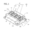
- FIG. 1 is a perspective view of a semiconductor module according to Embodiment Example 1 of the invention.
- FIG. 3 is a plan view of the semiconductor module with a plastic housing removed, according to Embodiment Example 1 of the invention.
- FIG. 3 omits wiring with aluminum wire bonding, solder, and a metallic wiring pattern for the purpose of avoiding complexity of the drawing.
- FIG. 4 is a front view of the semiconductor module with a plastic housing removed.
- FIG. 5 is a side view of the semiconductor module with a plastic housing removed seen from the side of auxiliary terminals, wherein aluminum wires are omitted in the drawing.
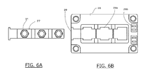
- FIG. 6B is a plan view of the plastic housing of the semiconductor module with a nut globe 27 removed from the plastic housing; and
- FIG. 6A is a plan view of the nut globe 27, which is a nut-receiving plastic body having nuts embedded at recessed places on the nut globe.
- FIG. 7 is a plan view of the semiconductor module with the nut globe 27 inserted from the side opposite to the auxiliary terminals and fitted to the plastic housing 26.
- FIG. 8 shows an equivalent circuit of the semiconductor module of the invention.
- a semiconductor module composed with the construction of the equivalent circuit of IFG. 8 is only an example of embodiment of the invention, and other circuit constructions should not be excluded.
- This semiconductor module has semiconductor elements including IGBTs and free-wheeling diodes (FWDs) that construct the equivalent circuit of FIG. 8 mounted and soldered on a wiring pattern on an insulated circuit board and contained in the plastic housing.
- semiconductor elements including IGBTs and free-wheeling diodes (FWDs) that construct the equivalent circuit of FIG. 8 mounted and soldered on a wiring pattern on an insulated circuit board and contained in the plastic housing.
- the semiconductor module 200 of Embodiment Example 1 is described in detail below referring to FIGS. 1 through 5 .
- This semiconductor module 200 comprises a metallic base plate 20, an insulated circuit board 21 fixed on the metallic base plate 20, semiconductor elements 22 such as an IGBT and a FWD fixed at specified places on the insulated circuit board 21 with solder, terminals of main terminals 24 for main current and auxiliary terminals 25 including control terminals, and a plastic housing 26 having a bottom opening with dimensions to fit to a bottom plate of the metallic base plate 20.
- the plastic housing 26 has a nut globe 27 that is inserted from an inserting hole 29 at the center-left side of the plastic housing 26 as shown in FIGS. 6 and 7 . Inserting process is as follows.
- the plastic housing 26 is fitted onto the metallic base plate 20 having the semiconductor elements assembled thereon, and the leading out main terminals 24 of C1, E2, and C1E2 and the auxiliary terminals 25 of g1, e1, e2, and g2 are led out from the openings 28a and 28b for terminals provided on the surface of the plastic housing 26.
- the nut globe 27 is inserted from the inserting hole 29 at the left side of the plastic housing 26.
- the positions of nut seat recesses 31 in the nut globe 27 are adjusted just beneath the attaching holes 30 for external terminals in the top parts 24a ( FIGS. 3 and 5 ) of the lead-out main terminals 24 (hereinafter simply referred to as main terminals).
- main terminals In order to facilitate to insert the nut globe 27 from the inserting hole 29 at the side of the plastic housing 26, a step is formed on the center surface 32 (in FIG. 1 ) of the plastic housing 26, the center surface 32 being used for inserting the nut globe 27 and higher than the peripheral surface 33.
- the nut globe 27 has the nut seat recesses 31 at the positions corresponding to the attaching holes 30 for external terminals formed in the top part 24a of the main terminal 24, each nut seat recess 31 having an embedded nut.
- a screw of the external terminal is screwed into the nut to fasten the main terminal 24 with the screw and nut to connect the main terminal 24 to the external terminal.
- the present invention needs a construction having a step between the central surface 32 and the peripheral surface 33 of the plastic housing 26, the central surface 32 being higher than the peripheral surface 33 and the step being disposed at a certain distance from the auxiliary terminals. Nevertheless, the present invention does not have necessarily a construction that uses the nut globe (or a resin body for nut receiving).
- the auxiliary terminals 25 are four terminals g1, e1, e2, and g2 and leading out from openings 28b of the plastic housing as shown in FIGS. 1 and 7 .
- the auxiliary terminal 25 has a projection 25a that comes in contact with the side of the plastic housing 26 at the opening 28b for the auxiliary terminal when the auxiliary terminal 25 is inserted through the opening 28b.
- the projection 25a is shown in FIG. 4 and provided for the purpose of fixing the auxiliary terminal 25.
- a recess 40 which is a first recess, is formed in the plastic housing 26 at the side of the opening 28b to receive the projection 25a and to be engaged with the projection thereby rigidly fastening the auxiliary terminal 25.
- the auxiliary terminals 25 are appropriately fixed, even though a downward force is exerted on the auxiliary terminals 25 in the process of inserting a connector to the auxiliary terminals 25 to connect the auxiliary terminals 25 to external terminals (not shown in the figures), the exerted force is scarcely transmitted to the bottom part of the auxiliary terminals or the insulated circuit board below the auxiliary terminals inside the plastic housing 26.
- the openings 28b are formed with slightly larger dimensions than the cross-section of the auxiliary terminal in order to facilitate inserting the auxiliary terminals 25.
- the fixing force on the auxiliary terminals with the projection 25a diminishes and the projection 25a does not properly carry out the function to block an external force.
- the loss of the function to block the external force would cause bending at the bottom portion of the auxiliary terminal 25 to lower the top position of the auxiliary terminal, which leads to poor external connection.
- the insulated circuit board may also be broken.
- the step between the central surface 32 and the peripheral surface 33 of the plastic housing 26 is utilized, and a holding piece 340 is interposed between the step and the auxiliary terminals 25.
- the projection 25a properly performs the function to block an external force, preventing the auxiliary terminals 25 from being led into poor external connection and the insulated circuit board 21 from being broken.
- the holding piece 340 is made of an insulating material such as a resin.
- FIG. 2A is a perspective view of the holding piece 340 and FIG. 2B is a sectional view of an essential part including the holding piece 340 of a semiconductor module. As shown in FIGS. 2A and 2B , the holding piece 340 has a rectangular cross-section.
- a second recess 260 is formed from the partial upper surface 26a of the plastic housing 26.
- the holding piece 340 is inserted into the second recess 260 so that the holding piece 340 pushes the projection 25a formed on the auxiliary terminal 25 against the first recess 40 in the plastic housing 26.
- This construction keeps the projection 25a engaged with the first recess 40 of the plastic housing 26 even when an external force acts on the auxiliary terminal 25 in the leftward direction in FIG. 2B .
- an external force acting on the auxiliary terminal 25 in the vertical direction does not generated large stress at the bottom part of the auxiliary terminal 25.
- a holding piece 341 in Embodiment Example 2 has a surface 50 to become in contact with the auxiliary terminals 25 and another surface 51 opposite to the surface 50, the surface 51 being so tilting that the cross-section of the holding piece 341 becomes smaller in the lower position.
- the surface 52 of the plastic housing 26 opposing the tilted surface 51 is also tilted so as to fit to the surface 51 of the holding piece 341.
- Embodiment Example 2 eliminates poor external connection of the auxiliary terminals 25 and breakage of the insulated circuit board 21.
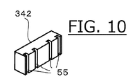
- Embodiment Example 3 a holding piece 342 in Embodiment Example 3 has slots 55 formed at the places corresponding to the respective auxiliary terminals 25 to fit to the terminals. This construction restricts movement of the auxiliary terminals 25 in the direction of the shorter side of the opening 28b for an auxiliary terminal due to an external force in the same direction.
- the slots 55 can be formed in the holding piece 341 of Embodiment Example 2 to obtain the same effects as in Embodiment Example 2.
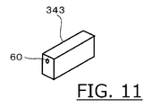
- a holding piece 343 in Embodiment Example 4 has third recesses 60 at least on two surfaces next to the surface in contact with the auxiliary terminals 25.
- the plastic housing 26 has projections corresponding to these third recesses 60.
- This construction securely fixes the holding piece 343, and is favorable because the construction fixes the auxiliary terminals 25 rigidly in the width direction i.e. shorter side direction of the terminals.
- the third recesses 60 and the projections formed on the plastic housing corresponding to the recesses 60 can be exchanged with each other, i.e., protrusions are formed on the holding piece 343 and recesses are formed on the plastic housing 26.
- the projection can have a configuration with a flat top surface and a tilted downward surface, the recess having a configuration to fit to such a projection.
- this construction can be applied to Embodiment Examples 2 and 3.
- Embodiment Example 5 the holding pieces 340, 341, 342, and 343 in Embodiment Examples 1 through 4 are adhered to the recessed parts formed in the plastic housing 26 corresponding to the holding pieces. Adhering the holding piece keeps securely the projection 25a engaged with the first recess 40 of the plastic housing 26 even when an external force acts on the auxiliary terminal 25 in the leftward direction in FIG. 2B , for example. Thus, an external force acting on the auxiliary terminal 25 in the vertical direction does not generate large stress at the bottom part of the auxiliary terminal 25.
- the inventor of the present invention has studied about relationship between a downward load [N] on an auxiliary terminal 25 and a sunken stroke [mm] of the auxiliary terminal 25 for cases of with and without a holding piece of the invention.
- Large sunken stroke of the auxiliary terminal 25 means poor performance to block stress generation by the projection 25a of the auxiliary terminal 25.
- FIG. 13 shows the measurement result.
- FIG. 13 shows that the structure having a holding piece (340, 341, 342, 343) between the auxiliary terminal 25 and a part of the plastic housing according to the invention performs effective function to block stress generation by the projection 25a against a downward load on the auxiliary terminal 25 larger than 100 [N]; the sunken stroke of the auxiliary terminal 25 was only 0.4 [mm] with a load of 120 [N].
- the load on the auxiliary terminal 25 was not able to increase to 40 [N] while the sunken stroke reached 1 [mm], indicating loss of the function to block stress generation by the projection 25a.
- the holding pieces 340, 341, 342, and 343 can be made of the same material as of the plastic housing 26.
- An insulating resin material different from that of the plastic housing 26 can also be used.
- the material can be a ceramic plate.
- a length of the holding piece is sufficient with a dimension that allows fixing all auxiliary terminals 25.
- the insulated circuit board 21 is fixed on the metallic base plate 20; the semiconductor elements such as an IGBT and a FWD are fixed with solder at predetermined places on the insulated circuit board 21; and the main terminals 24 for main current and the auxiliary terminals 25 including control terminals are fixed at predetermined places. Then, the circuit components are assembled on the metallic base plate 20. With the base plate of assembled metallic base plate 20, the plastic housing 26 (or 260a and 260b in FIG. 9A ) having the bottom opening is engaged.
- the main terminals 24 are exposed from the openings 28a for the main terminals provided on the higher flat surface 32 of the plastic housing 26 (or 260a and 260b); and the auxiliary terminals 25 are exposed from the openings 28b for the auxiliary terminals provided on the lower flat surface 33 of the plastic housing 26 (or 260a and 260b).
- the nut globe 27, which is a nut-receiving resin body, is inserted from the inserting hole 29 formed at the side surface opposite to the side of the auxiliary terminals 25.
- the holding piece 340 (or 341, 342, 343) is fitted between the higher flat surface 32 and the auxiliary terminals 25.
- auxiliary terminals 25 are surely fixed in the longitudinal direction of the slit of the opening 28b for auxiliary terminal 25. Therefore, an external downward force exerted on the auxiliary terminals 25 during a connecting process of an external connector to the auxiliary terminals does never cause poor connection of external terminals and breakage of the insulated circuit board.
Landscapes
- Structures Or Materials For Encapsulating Or Coating Semiconductor Devices Or Solid State Devices (AREA)
Abstract
Description
- This application is based on, and claims priority to, Japanese Patent Application No.
2012-277224, filed on December 19, 2012 - The present invention relates to a semiconductor module such as a power semiconductor module containing a plurality of semiconductor elements in a single package.
-
FIG. 12A is a perspective view of a knownsemiconductor module 100 for motor drive control containing a plurality of power semiconductor elements, for example, insulated gate bipolar transistors (IGBTs). Thissemiconductor module 100 comprises ametallic base plate 20, aninsulated circuit board 21 on thebase plate 20, and a plurality ofpower semiconductor elements 22 fixed at predetermined positions on theinsulated circuit board 21 with solder as shown inFIG. 4 . Thesemiconductor module 100 further comprises metallicmain terminals 102,control terminals 103, and aplastic housing 104 that is a frame for protecting thepower semiconductor elements 22 and for fixing themain terminals 102 and thecontrol terminals 103 that are leading out of the housing. The space in theplastic housing 104 is filled with a resin composite in a gel state. The power semiconductor elements are mounted on a metallic circuit pattern formed on theinsulated circuit board 21 and connected withaluminum wires 23 between the metallic circuit pattern and metallic electrodes on thesemiconductor elements 22. -
FIG. 8 shows an equivalent circuit of a semiconductor module composed of semiconductor elements of IGBTs T1 and T2 and free wheel diodes (FWDs) D1 and D2 anti-parallel-connected to the IGBTs T1 and T2, respectively. A resin composite in a gel state fills a space between theplastic housing 104 and a bottom plate that is themetallic base plate 20 for mounting thesepower semiconductor elements 22. The metallicmain terminals 102, which are a C1 terminal, an E2 terminal, and a C1E2 terminal as shown inFIG. 12A , are connected externally through ascrew holes 105 formed in the metallicmain terminals 102 exposing to the center surface of theplastic housing 104. Theauxiliary terminals 103, which are a g1 terminal, an e1 terminal, an e2 terminal, and a g2 terminal, are led out through theslits 106 formed in the end region of the surface of theplastic housing 104. Themetallic base plate 20 has four holes for attaching itself to a heat sink at the corners of thebase plate 20. Theplastic housing 104 has an opening at the bottom thereof for theplastic housing 104 to be fitted to the base plate. - Patent Document 1 discloses a semiconductor device in which electrode terminals are ensured to be held on a thermoplastic resin housing to enhance reliability in assembling quality, and the electrode terminals are prevented from falling off from the resin housing due to vibration.
- Patent Document 2 discloses a semiconductor module that includes a plastic housing, connection elements for external main connections and control connections, and an insulated substrate with a metallized surface. The insulated substrate mounting semiconductor elements is inserted into a bottom opening of the plastic housing.
- Patent Document 3 discloses a semiconductor module with a high dielectric strength and high reliability in which a control terminal has a projection at a position of passing through the plastic housing and an L-shaped portion is provided in the control terminal in order to avoid transmission of stress onto the insulated circuit board in attaching and detaching processes of a connector.
- [Patent Document 1]
Japanese Utility Model Application Publication No.H05-006852 FIG. 1 , in particular) - [Patent Document 2]
United States Patent No.6,597,585 (Claim 1 andFIG. 3 , in particular) - [Patent Document 3]
W02012/0066833 FIG. 1 , in particular) - In the
semiconductor module 100 shown by the perspective view ofFIG. 12A , the resin injected in theresin housing 104 is a resin composite in a gel state exhibiting flexibility that cannot rigidly fix the leading out terminals of the metallicmain terminals 102 and thecontrol terminals 103. Thus, the leading out terminals need to be fixed at the openings in theplastic housing 104 formed for leading out the terminals. Of the leading out terminals, the metallicmain terminals 102 are held with theresin housing 104 and thus, the stress exerted in the processes of external connection is scarcely transmitted to the bottom portion of the main terminal. - As for the
auxiliary terminals 103, however, after fixing theauxiliary terminals 103 onto theinsulated circuit board 21, theauxiliary terminals 103 need to be easily inserted through theopenings 107 for the auxiliary terminals formed in theplastic housing 104 and also to be securely held on the housing. To meet these requirements, theopenings 107 for the auxiliary terminals, as shown inFIG. 12A , each have a configuration of a slit with a size that is slightly larger than the cross-sectional size of the terminal. In addition, theauxiliary terminal 103 is provided with a projection and the plastic housing is provided with a notch to hold the terminal on the housing as shown inFIG. 12B . InFIG. 12B , thesymbols auxiliary terminals 103 each have aprojection 103a inside theplastic housing 104, and theplastic housing 104 has arecess 108 opposing theprojection 103a. The recess 108 restricts vertical movement of theprojection 103a. In the method of holding the terminals utilizing the projection and notch, however, the terminals are apt to become out of place in the longitudinal direction of the slit because the slit is formed with a little larger dimension. This is the case an external force is exerted toward the left at the upper position of theauxiliary terminal 103 inFIG. 12B . If the slit length is decreased to avoid disengagement of the auxiliary terminal, insertion can be hardly carried out, and some stress may be exerted on the bottom portion of the auxiliary terminals in the inserting process. Thus, the reduction of the slit length is restricted. - The present invention has been made in view of the foregoing and an object of the present invention is to provide a semiconductor module that solves the above-mentioned problems and that allows easy engagement between the auxiliary terminals and the plastic housing in the assembling process and avoids transmission of stress onto the bottom portion of the auxiliary terminals or onto the insulated circuit board in the process of attaching an external connector. A method of manufacturing such a semiconductor module is also provided.
- A semiconductor module according to a first aspect of the present invention comprises: a semiconductor element(s) mounted on an insulated circuit board adhered on a metallic base plate; a plastic housing to accommodate the semiconductor element; and a terminal(s) leading out vertically from an upper surface of the plastic housing; wherein the plastic housing is provided with an opening(s) for leading out the terminal(s) on the upper surface of the plastic housing; the terminal has a projection thereon at a position inside the plastic housing to restrict vertical movement of the terminal; the plastic housing is provided with a first recess that engages with the projection; the semiconductor module comprises a holding piece made of an insulating material having a cross-section of a triangle or a rectangle and one surface thereof being in contact with the terminal; the plastic housing is provided with a second recess on an upper surface thereof, the second recess receiving the holding piece so that the holding piece pushes the projection on the auxiliary terminal toward the firsts recess.
- A semiconductor module according to a second aspect of the present invention is the semiconductor module of the first aspect of the invention, wherein the holding piece has a titling surface on a surface opposite to a surface that is in contact with the terminal, the titling surface making the cross-section of the holding piece narrower in the lower position, and a surface of the plastic housing opposing the tilting surface of the holding piece has a tilting surface that fits to the tilting surface of the holding piece.
- A semiconductor module according to a third aspect of the present invention is the semiconductor module of the first or second aspect of the invention, wherein the holding piece has a slot(s) at a position(s) corresponding to the terminal(s), which is inserted into the slot.
- A semiconductor module according to a fourth aspect of the present invention is the semiconductor module of the any one of the first through third aspect of the invention, wherein the holding piece has projections or recesses on at least two surfaces thereof, and the plastic housing has recesses or projections that fit to the projections or recesses on the holding piece.
- A semiconductor module according to a fifth aspect of the present invention is the semiconductor module of the any one of the first through fourth aspect of the invention, wherein the holding piece is adhered to the second recess on the plastic housing.
- A sixth aspect of the present invention is a method of manufacturing a semiconductor module comprising steps of: fixing a semiconductor element(s) and a terminal(s) on an insulated circuit board adhered on a metallic base plate; and adhering a plastic housing that accommodates the semiconductor element(s) and leads out the terminal vertically from an opening provided on an upper surface of the plastic housing onto the metallic base plate; wherein after the terminal is led out from the openings using the plastic housing defined by claims 1 through 4, the holding piece defined by claims 1 through 4 is inserted into the second recess defined by claims 1 through 4 in such a way that the holding piece pushes the projection formed on the terminal toward the first recess on the plastic housing.
- The present invention provides a semiconductor module and a method of manufacturing the same in which the plastic housing is easily engaged with the auxiliary terminals in the assembly process and stress transmission onto the bottom portion of the auxiliary terminals or onto the insulation circuit board is avoided in the process of attaching an external connector.
-
-
FIG. 1 is a perspective view of a semiconductor module according to Embodiment Example 1 of the present invention; -
FIG. 2A is a perspective view of a holding piece in the semiconductor module according to Embodiment Example 1 of the invention; -
FIG. 2b is a sectional view of an essential part of the semiconductor module according to Embodiment Example 1 of the invention; -
FIG. 3 is a plan view of a semiconductor module with the plastic housing removed according to Embodiment Example 1 of the invention; -
FIG. 4 is a front view of a semiconductor module with the plastic housing removed according to Embodiment Example 1 of the invention; -
FIG. 5 is a side view, seen from the side of the auxiliary terminals, of a semiconductor module with plastic housing removed according to Embodiment Example 1 of the invention; -
FIG. 6A is a plan view of the nut globe of the plastic housing of the semiconductor module according to Embodiment Example 1 of the invention; -
FIG. 6B is a plan view of the plastic housing with the nut globe removed of the semiconductor module according to Embodiment Example 1 of the invention; -
FIG. 7 is a plan view of the plastic housing with the nut globe engaged therewith of the semiconductor module according to Embodiment Example 1 of the invention; -
FIG. 8 shows an equivalent circuit of the semiconductor module according to Embodiment Example 1 of the invention; -
FIG. 9A is a sectional view of an essential part of a semiconductor module according to Embodiment Example 2 of the invention; -
FIG. 9B is a perspective view of a holding piece according to Embodiment Example 2 of the invention; -
FIG. 10 is a perspective view of a holding piece according to Embodiment Example 3 of the invention; -
FIG. 11 is a perspective view of a holding piece according to Embodiment Example 4 of the invention; -
FIG. 12A is a perspective view of a semiconductor module according to a conventional technology; -
FIG. 12B is a sectional view of an essential part of the semiconductor module ofFIG. 12A ; and -
FIG. 13 shows a relationship between a downward load [N] on an auxiliary terminal and a sunken stroke [mm] of the auxiliary terminal in a semiconductor module of the invention and in a conventional semiconductor module. - The following describes details of semiconductor modules according to some preferred embodiments of the present invention with reference to accompanying drawings. In the description and drawings of the embodiment examples below, the same constructions are given the same symbols and repeated description thereon is avoided. The drawings are not depicted with an accurate scale for better understanding. The present invention is not limited to the embodiment examples described below but various modifications are possible without departing from the spirit and scope of the invention.
-
FIG. 1 is a perspective view of a semiconductor module according to Embodiment Example 1 of the invention.FIG. 3 is a plan view of the semiconductor module with a plastic housing removed, according to Embodiment Example 1 of the invention.FIG. 3 , however, omits wiring with aluminum wire bonding, solder, and a metallic wiring pattern for the purpose of avoiding complexity of the drawing. -
FIG. 4 is a front view of the semiconductor module with a plastic housing removed.FIG. 5 is a side view of the semiconductor module with a plastic housing removed seen from the side of auxiliary terminals, wherein aluminum wires are omitted in the drawing.FIG. 6B is a plan view of the plastic housing of the semiconductor module with anut globe 27 removed from the plastic housing; andFIG. 6A is a plan view of thenut globe 27, which is a nut-receiving plastic body having nuts embedded at recessed places on the nut globe.FIG. 7 is a plan view of the semiconductor module with thenut globe 27 inserted from the side opposite to the auxiliary terminals and fitted to theplastic housing 26.FIG. 8 shows an equivalent circuit of the semiconductor module of the invention. A semiconductor module composed with the construction of the equivalent circuit of IFG. 8 is only an example of embodiment of the invention, and other circuit constructions should not be excluded. - This semiconductor module has semiconductor elements including IGBTs and free-wheeling diodes (FWDs) that construct the equivalent circuit of
FIG. 8 mounted and soldered on a wiring pattern on an insulated circuit board and contained in the plastic housing. - The
semiconductor module 200 of Embodiment Example 1 is described in detail below referring toFIGS. 1 through 5 . - This
semiconductor module 200 comprises ametallic base plate 20, aninsulated circuit board 21 fixed on themetallic base plate 20,semiconductor elements 22 such as an IGBT and a FWD fixed at specified places on the insulatedcircuit board 21 with solder, terminals ofmain terminals 24 for main current andauxiliary terminals 25 including control terminals, and aplastic housing 26 having a bottom opening with dimensions to fit to a bottom plate of themetallic base plate 20. - The
plastic housing 26 has anut globe 27 that is inserted from an insertinghole 29 at the center-left side of theplastic housing 26 as shown inFIGS. 6 and7 . Inserting process is as follows. Theplastic housing 26 is fitted onto themetallic base plate 20 having the semiconductor elements assembled thereon, and the leading outmain terminals 24 of C1, E2, and C1E2 and theauxiliary terminals 25 of g1, e1, e2, and g2 are led out from theopenings plastic housing 26. Then, thenut globe 27 is inserted from the insertinghole 29 at the left side of theplastic housing 26. The positions of nut seat recesses 31 in thenut globe 27 are adjusted just beneath the attachingholes 30 for external terminals in thetop parts 24a (FIGS. 3 and5 ) of the lead-out main terminals 24 (hereinafter simply referred to as main terminals). In order to facilitate to insert thenut globe 27 from the insertinghole 29 at the side of theplastic housing 26, a step is formed on the center surface 32 (inFIG. 1 ) of theplastic housing 26, thecenter surface 32 being used for inserting thenut globe 27 and higher than theperipheral surface 33. Thenut globe 27 has the nut seat recesses 31 at the positions corresponding to the attachingholes 30 for external terminals formed in thetop part 24a of themain terminal 24, each nut seat recess 31 having an embedded nut. A screw of the external terminal is screwed into the nut to fasten themain terminal 24 with the screw and nut to connect themain terminal 24 to the external terminal. The present invention needs a construction having a step between thecentral surface 32 and theperipheral surface 33 of theplastic housing 26, thecentral surface 32 being higher than theperipheral surface 33 and the step being disposed at a certain distance from the auxiliary terminals. Nevertheless, the present invention does not have necessarily a construction that uses the nut globe (or a resin body for nut receiving). - The
auxiliary terminals 25 are four terminals g1, e1, e2, and g2 and leading out fromopenings 28b of the plastic housing as shown inFIGS. 1 and7 . Theauxiliary terminal 25 has aprojection 25a that comes in contact with the side of theplastic housing 26 at theopening 28b for the auxiliary terminal when theauxiliary terminal 25 is inserted through theopening 28b. Theprojection 25a is shown inFIG. 4 and provided for the purpose of fixing theauxiliary terminal 25. Arecess 40, which is a first recess, is formed in theplastic housing 26 at the side of theopening 28b to receive theprojection 25a and to be engaged with the projection thereby rigidly fastening theauxiliary terminal 25. - If the
auxiliary terminals 25 are appropriately fixed, even though a downward force is exerted on theauxiliary terminals 25 in the process of inserting a connector to theauxiliary terminals 25 to connect theauxiliary terminals 25 to external terminals (not shown in the figures), the exerted force is scarcely transmitted to the bottom part of the auxiliary terminals or the insulated circuit board below the auxiliary terminals inside theplastic housing 26. However, theopenings 28b are formed with slightly larger dimensions than the cross-section of the auxiliary terminal in order to facilitate inserting theauxiliary terminals 25. As a result, when a certain force in the direction of longer side of theopenings 28b is exerted on theauxiliary terminal 25, the fixing force on the auxiliary terminals with theprojection 25a diminishes and theprojection 25a does not properly carry out the function to block an external force. The loss of the function to block the external force would cause bending at the bottom portion of theauxiliary terminal 25 to lower the top position of the auxiliary terminal, which leads to poor external connection. The insulated circuit board may also be broken. - Accordingly, in an embodiment of the present invention, the step between the
central surface 32 and theperipheral surface 33 of theplastic housing 26 is utilized, and aholding piece 340 is interposed between the step and theauxiliary terminals 25. Owing to this construction, theprojection 25a properly performs the function to block an external force, preventing theauxiliary terminals 25 from being led into poor external connection and the insulatedcircuit board 21 from being broken. The holdingpiece 340 is made of an insulating material such as a resin.FIG. 2A is a perspective view of the holdingpiece 340 andFIG. 2B is a sectional view of an essential part including the holdingpiece 340 of a semiconductor module. As shown inFIGS. 2A and 2B , the holdingpiece 340 has a rectangular cross-section. One of the surfaces of the holdingpiece 340 is in contact with theauxiliary terminals 25. Asecond recess 260 is formed from the partialupper surface 26a of theplastic housing 26. The holdingpiece 340 is inserted into thesecond recess 260 so that the holdingpiece 340 pushes theprojection 25a formed on theauxiliary terminal 25 against thefirst recess 40 in theplastic housing 26. This construction keeps theprojection 25a engaged with thefirst recess 40 of theplastic housing 26 even when an external force acts on theauxiliary terminal 25 in the leftward direction inFIG. 2B . Thus, an external force acting on theauxiliary terminal 25 in the vertical direction does not generated large stress at the bottom part of theauxiliary terminal 25. - The following describes a second example of embodiment of the present invention, Embodiment Example 2. As shown in
FIG. 9B , a holdingpiece 341 in Embodiment Example 2 has asurface 50 to become in contact with theauxiliary terminals 25 and anothersurface 51 opposite to thesurface 50, thesurface 51 being so tilting that the cross-section of the holdingpiece 341 becomes smaller in the lower position. Thesurface 52 of theplastic housing 26 opposing the tiltedsurface 51 is also tilted so as to fit to thesurface 51 of the holdingpiece 341. - This construction allows the
projection 25a pushed against thefirst recess 40 more strongly as the holdingpiece 341 is inserted into thesecond recess 261 in comparison with the construction of Embodiment Example 1. By setting an inserting depth of the holdingpiece 341 properly, a large dimensional tolerance is allowed in the width of the holdingpiece 341 and the width of thesecond recess 261 in the horizontal direction inFIG. 9A . This construction keeps more securely theprojection 25a engaged with thefirst recess 40 of theplastic housing 26 even when an external force acts on theauxiliary terminals 25 in the leftward direction inFIG. 9A . Thus, an external force acting on theauxiliary terminal 25 in the vertical direction does not generate large stress at the bottom part of theauxiliary terminal 25. Therefore, the construction of Embodiment Example 2 eliminates poor external connection of theauxiliary terminals 25 and breakage of the insulatedcircuit board 21. - The following describes a third example of embodiment of the present invention, Embodiment Example 3. As shown in
FIG. 10 , a holdingpiece 342 in Embodiment Example 3 hasslots 55 formed at the places corresponding to the respectiveauxiliary terminals 25 to fit to the terminals. This construction restricts movement of theauxiliary terminals 25 in the direction of the shorter side of theopening 28b for an auxiliary terminal due to an external force in the same direction. Theslots 55 can be formed in the holdingpiece 341 of Embodiment Example 2 to obtain the same effects as in Embodiment Example 2. - The following describes a fourth example of embodiment of the present invention, Embodiment Example 4. As shown in
FIG. 11 , a holdingpiece 343 in Embodiment Example 4 hasthird recesses 60 at least on two surfaces next to the surface in contact with theauxiliary terminals 25. Theplastic housing 26 has projections corresponding to these third recesses 60. This construction securely fixes the holdingpiece 343, and is favorable because the construction fixes theauxiliary terminals 25 rigidly in the width direction i.e. shorter side direction of the terminals. The third recesses 60 and the projections formed on the plastic housing corresponding to therecesses 60 can be exchanged with each other, i.e., protrusions are formed on the holdingpiece 343 and recesses are formed on theplastic housing 26. In addition, the projection can have a configuration with a flat top surface and a tilted downward surface, the recess having a configuration to fit to such a projection. Moreover, this construction can be applied to Embodiment Examples 2 and 3. - The following describes a fifth example of embodiment of the present invention, Embodiment Example 5. In Embodiment Example 5, the holding
pieces plastic housing 26 corresponding to the holding pieces. Adhering the holding piece keeps securely theprojection 25a engaged with thefirst recess 40 of theplastic housing 26 even when an external force acts on theauxiliary terminal 25 in the leftward direction inFIG. 2B , for example. Thus, an external force acting on theauxiliary terminal 25 in the vertical direction does not generate large stress at the bottom part of theauxiliary terminal 25. - The inventor of the present invention has studied about relationship between a downward load [N] on an
auxiliary terminal 25 and a sunken stroke [mm] of theauxiliary terminal 25 for cases of with and without a holding piece of the invention. Large sunken stroke of theauxiliary terminal 25 means poor performance to block stress generation by theprojection 25a of theauxiliary terminal 25.FIG. 13 shows the measurement result. -
FIG. 13 shows that the structure having a holding piece (340, 341, 342, 343) between theauxiliary terminal 25 and a part of the plastic housing according to the invention performs effective function to block stress generation by theprojection 25a against a downward load on theauxiliary terminal 25 larger than 100 [N]; the sunken stroke of theauxiliary terminal 25 was only 0.4 [mm] with a load of 120 [N]. In contrast, a conventional construction without the holding piece, the load on theauxiliary terminal 25 was not able to increase to 40 [N] while the sunken stroke reached 1 [mm], indicating loss of the function to block stress generation by theprojection 25a. - The holding
pieces plastic housing 26. An insulating resin material different from that of theplastic housing 26 can also be used. The material can be a ceramic plate. A length of the holding piece is sufficient with a dimension that allows fixing allauxiliary terminals 25. - Now, a method of manufacturing a semiconductor module according to the present invention will be described below. The insulated
circuit board 21 is fixed on themetallic base plate 20; the semiconductor elements such as an IGBT and a FWD are fixed with solder at predetermined places on the insulatedcircuit board 21; and themain terminals 24 for main current and theauxiliary terminals 25 including control terminals are fixed at predetermined places. Then, the circuit components are assembled on themetallic base plate 20. With the base plate of assembledmetallic base plate 20, the plastic housing 26 (or 260a and 260b inFIG. 9A ) having the bottom opening is engaged. Themain terminals 24 are exposed from theopenings 28a for the main terminals provided on the higherflat surface 32 of the plastic housing 26 (or 260a and 260b); and theauxiliary terminals 25 are exposed from theopenings 28b for the auxiliary terminals provided on the lowerflat surface 33 of the plastic housing 26 (or 260a and 260b). Then, thenut globe 27, which is a nut-receiving resin body, is inserted from the insertinghole 29 formed at the side surface opposite to the side of theauxiliary terminals 25. After that, the holding piece 340 (or 341, 342, 343) is fitted between the higherflat surface 32 and theauxiliary terminals 25. Thus, theauxiliary terminals 25 are surely fixed in the longitudinal direction of the slit of theopening 28b forauxiliary terminal 25. Therefore, an external downward force exerted on theauxiliary terminals 25 during a connecting process of an external connector to the auxiliary terminals does never cause poor connection of external terminals and breakage of the insulated circuit board. - Features, components and specific details of the structures of the above-described embodiments may be exchanged or combined to form further embodiments optimized for the respective application. As far as those modifications are readily apparent for an expert skilled in the art they shall be disclosed implicitly by the above description without specifying explicitly every possible combination, for the sake of conciseness of the present description.
-
- 20:
- metallic base plate
- 21:
- insulated circuit board
- 22:
- semiconductor element
- 23:
- aluminum wire
- 24:
- main terminal
- 24a:
- top part of the main terminal
- 25:
- auxiliary terminal
- 25a:
- projection
- 26:
- plastic housing
- 27:
- nut globe
- 28a:
- opening for a main terminal
- 28b:
- opening for an auxiliary terminal
- 29:
- inserting hole
- 30:
- attaching hole for an external terminal
- 31:
- nut seat recess
- 32:
- higher flat surface
- 33:
- lower flat surface
- 340, 341, 342, 343:
- holding piece
- C1:
- collector terminal
- E2:
- emitter terminal
- g1, g2:
- gate terminal
- e1, e2:
- emitter auxiliary terminal
- 100, 200:
- semiconductor module
Claims (6)
- A semiconductor module comprising:at least one semiconductor element (22) mounted on an insulated circuit board adhered on a metallic base plate;a plastic housing (26) to accommodate the semiconductor element (22); andat least one terminal leading out vertically from an upper surface of the plastic housing (26);
whereinthe plastic housing (26) is provided with an opening for leading out the terminal on the upper surface of the plastic housing (26);the terminal has a projection thereon at a position inside the plastic housing (26) to restrict vertical movement of the terminal;the plastic housing (26) is provided with a first recess that engages with the projection;the semiconductor module (100; 200) comprises a holding piece (340) made of an insulating material having a cross-section of a triangle or a rectangle and one surface thereof being in contact with the terminal;the plastic housing (26) is provided with a second recess on an upper surface thereof, the second recess receiving the holding piece (340) so that the holding piece (340) pushes the projection on the auxiliary terminal (25) toward the firsts recess. - The semiconductor module according to claim 1, wherein the holding piece (340) has a titling surface on a surface opposite to a surface that is in contact with the terminal, the titling surface making the cross-section of the holding piece narrower in the lower position, and a surface of the plastic housing (26) opposing the tilting surface of the holding piece has a tilting surface that fits to the tilting surface of the holding piece (340).
- The semiconductor module according to claim 1 or claim 2, wherein the holding piece (340) has at least one slot at a position corresponding to the terminal, which are inserted into the slot.
- The semiconductor module according to any one of claims 1 through 3, wherein the holding piece (340) has projections or recesses on at least two surfaces thereof, and the plastic housing (26) has recesses or projections that fit to the projections or recesses on the holding piece (340).
- The semiconductor module according to any one of claims 1 through 4, wherein the holding piece (340) is adhered to the second recess on the plastic housing (26).
- A method of manufacturing a semiconductor module comprising the steps of:fixing at least one semiconductor element (22) and at least one terminal on an insulated circuit board adhered on a metallic base plate (20); andadhering a plastic housing (26) that accommodates the semiconductor element (22) and leads out the terminal vertically from an opening provided on an upper surface of the plastic housing (26) onto the metallic base plate (20); whereinafter the terminal is led out from the openings using the plastic housing (26) defined by claims 1 through 4,the holding piece (340) defined by claims 1 through 4 is inserted into the second recess defined by claims 1 through 4 in such a way that the holding piece (340) pushes the projection formed on the terminal toward the first recess on the plastic housing (26).
Applications Claiming Priority (1)
| Application Number | Priority Date | Filing Date | Title |
|---|---|---|---|
| JP2012277224A JP6044321B2 (en) | 2012-12-19 | 2012-12-19 | Semiconductor module |
Publications (2)
| Publication Number | Publication Date |
|---|---|
| EP2747137A1 true EP2747137A1 (en) | 2014-06-25 |
| EP2747137B1 EP2747137B1 (en) | 2019-09-25 |
Family
ID=49752998
Family Applications (1)
| Application Number | Title | Priority Date | Filing Date |
|---|---|---|---|
| EP13195866.2A Not-in-force EP2747137B1 (en) | 2012-12-19 | 2013-12-05 | Semiconductor module |
Country Status (4)
| Country | Link |
|---|---|
| US (1) | US8975740B2 (en) |
| EP (1) | EP2747137B1 (en) |
| JP (1) | JP6044321B2 (en) |
| CN (1) | CN103887273B (en) |
Cited By (1)
| Publication number | Priority date | Publication date | Assignee | Title |
|---|---|---|---|---|
| RU172194U1 (en) * | 2016-12-29 | 2017-06-30 | Закрытое акционерное общество "Инновационная фирма "ИРСЭТ-Центр" | LIGHT-RADIATING MODULE |
Families Citing this family (21)
| Publication number | Priority date | Publication date | Assignee | Title |
|---|---|---|---|---|
| DE112015003244T5 (en) * | 2014-09-25 | 2017-04-13 | Hitachi Automotive Systems, Ltd. | power converter |
| WO2016059916A1 (en) | 2014-10-14 | 2016-04-21 | 富士電機株式会社 | Semiconductor device |
| JP6288301B2 (en) | 2014-11-28 | 2018-03-14 | 日産自動車株式会社 | Half-bridge power semiconductor module and manufacturing method thereof |
| JP6382097B2 (en) | 2014-12-24 | 2018-08-29 | 株式会社 日立パワーデバイス | Semiconductor power module and power converter using the same |
| WO2016129097A1 (en) * | 2015-02-13 | 2016-08-18 | 株式会社日産アーク | Half-bridge power semiconductor module, and method for manufacturing same |
| DE102015103068B4 (en) | 2015-03-03 | 2019-05-02 | Infineon Technologies Bipolar Gmbh & Co. Kg | Power semiconductor module with improved mechanical support of the control connection element and associated mounting method |
| US10629513B2 (en) * | 2015-06-04 | 2020-04-21 | Eaton Intelligent Power Limited | Ceramic plated materials for electrical isolation and thermal transfer |
| JP6578795B2 (en) * | 2015-08-04 | 2019-09-25 | 富士電機株式会社 | Semiconductor device and manufacturing method of semiconductor device |
| JP6683266B2 (en) * | 2017-01-17 | 2020-04-15 | 富士電機株式会社 | Semiconductor device |
| WO2018224511A1 (en) * | 2017-06-07 | 2018-12-13 | Abb Schweiz Ag | Power semiconductor module |
| DE112017007768T5 (en) | 2017-07-21 | 2020-04-16 | Mitsubishi Electric Corporation | Power converter |
| FR3076175B1 (en) * | 2017-12-22 | 2020-01-10 | Valeo Siemens Eautomotive France Sas | REMOTE WALL ELECTRICAL EQUIPMENT |
| JP7275493B2 (en) * | 2018-08-07 | 2023-05-18 | 富士電機株式会社 | semiconductor equipment |
| JP7238565B2 (en) * | 2019-04-12 | 2023-03-14 | 富士電機株式会社 | Semiconductor device and method for manufacturing semiconductor device |
| EP3797962A1 (en) * | 2019-09-30 | 2021-03-31 | Siemens Aktiengesellschaft | Electronic module housing and production thereof |
| EP4079118A1 (en) * | 2019-12-18 | 2022-10-26 | Eaton Intelligent Power Limited | Power converter system |
| CN111341764B (en) * | 2020-03-12 | 2022-03-15 | 西安石油大学 | Insulated gate bipolar thyristor module and electrode power terminal |
| DE102020211423A1 (en) * | 2020-09-11 | 2022-03-17 | Zf Friedrichshafen Ag | Process for manufacturing an inverter, positioning aid and inverter |
| USD1078669S1 (en) * | 2023-10-18 | 2025-06-10 | Semikron Danfoss International GmbH | Semiconductor power module for vehicles |
| CN117954399B (en) * | 2024-03-26 | 2024-06-25 | 淄博美林电子有限公司 | High temperature resistant IGBT, siC mixed power module |
| FR3167827A1 (en) * | 2024-10-17 | 2026-04-24 | Valeo Eautomotive Germany Gmbh | Electronic module, electronic system and associated manufacturing process. |
Citations (5)
| Publication number | Priority date | Publication date | Assignee | Title |
|---|---|---|---|---|
| JPH056852A (en) | 1991-06-27 | 1993-01-14 | Fujitsu Ltd | X-ray irradiation device and X-ray irradiation method |
| DE10100460A1 (en) * | 2001-01-08 | 2002-07-18 | Semikron Elektronik Gmbh | Power semiconductor module with housing and connections aligns connecting elements parallel to base plate |
| US6597585B2 (en) | 1999-03-17 | 2003-07-22 | Eupec Europaeische Gesellschaft Fuer Leistungshalbleiter Gmbh & Co. Kg | Power semiconductor module |
| EP2216814A2 (en) * | 2009-02-05 | 2010-08-11 | Mitsubishi Electric Corporation | Power semiconductor device and manufacturing method therefor |
| WO2012006683A1 (en) | 2010-07-16 | 2012-01-19 | Controlled Release Technologies Pty Ltd | Pharmaceutical compositions for sustained delivery of benzodiazepine antagonists |
Family Cites Families (12)
| Publication number | Priority date | Publication date | Assignee | Title |
|---|---|---|---|---|
| JPH01302753A (en) * | 1988-05-30 | 1989-12-06 | Sansha Electric Mfg Co Ltd | Resin-sealed semiconductor device |
| JPH087956A (en) * | 1994-06-23 | 1996-01-12 | Fuji Electric Co Ltd | Semiconductor device terminal assembly structure |
| JPH08162582A (en) * | 1994-12-02 | 1996-06-21 | Mitsubishi Electric Corp | Semiconductor device |
| JP2003068979A (en) * | 2001-08-28 | 2003-03-07 | Hitachi Ltd | Semiconductor device |
| DE10258570B4 (en) * | 2002-12-14 | 2005-11-03 | Semikron Elektronik Gmbh & Co. Kg | The power semiconductor module |
| JP2005142189A (en) * | 2003-11-04 | 2005-06-02 | Toyota Industries Corp | Semiconductor device |
| JP5028085B2 (en) * | 2006-12-27 | 2012-09-19 | アイシン・エィ・ダブリュ株式会社 | Electronic circuit device and manufacturing method thereof |
| JP4093319B1 (en) * | 2007-03-01 | 2008-06-04 | クオリティ株式会社 | Evacuation guidance system |
| DE102007010883A1 (en) * | 2007-03-06 | 2008-09-18 | Infineon Technologies Ag | Power semiconductor device and method for its production |
| US9147666B2 (en) * | 2009-05-14 | 2015-09-29 | Rohm Co., Ltd. | Semiconductor device |
| JP2012005301A (en) * | 2010-06-18 | 2012-01-05 | Fuji Electric Co Ltd | Power semiconductor module |
| EP2725610B1 (en) * | 2011-09-28 | 2020-06-03 | Fuji Electric Co., Ltd. | Semiconductor device and method for producing semiconductor device |
-
2012
- 2012-12-19 JP JP2012277224A patent/JP6044321B2/en not_active Expired - Fee Related
-
2013
- 2013-12-05 EP EP13195866.2A patent/EP2747137B1/en not_active Not-in-force
- 2013-12-16 CN CN201310689092.4A patent/CN103887273B/en not_active Expired - Fee Related
- 2013-12-17 US US14/109,233 patent/US8975740B2/en active Active
Patent Citations (5)
| Publication number | Priority date | Publication date | Assignee | Title |
|---|---|---|---|---|
| JPH056852A (en) | 1991-06-27 | 1993-01-14 | Fujitsu Ltd | X-ray irradiation device and X-ray irradiation method |
| US6597585B2 (en) | 1999-03-17 | 2003-07-22 | Eupec Europaeische Gesellschaft Fuer Leistungshalbleiter Gmbh & Co. Kg | Power semiconductor module |
| DE10100460A1 (en) * | 2001-01-08 | 2002-07-18 | Semikron Elektronik Gmbh | Power semiconductor module with housing and connections aligns connecting elements parallel to base plate |
| EP2216814A2 (en) * | 2009-02-05 | 2010-08-11 | Mitsubishi Electric Corporation | Power semiconductor device and manufacturing method therefor |
| WO2012006683A1 (en) | 2010-07-16 | 2012-01-19 | Controlled Release Technologies Pty Ltd | Pharmaceutical compositions for sustained delivery of benzodiazepine antagonists |
Cited By (1)
| Publication number | Priority date | Publication date | Assignee | Title |
|---|---|---|---|---|
| RU172194U1 (en) * | 2016-12-29 | 2017-06-30 | Закрытое акционерное общество "Инновационная фирма "ИРСЭТ-Центр" | LIGHT-RADIATING MODULE |
Also Published As
| Publication number | Publication date |
|---|---|
| CN103887273B (en) | 2018-04-24 |
| JP2014120734A (en) | 2014-06-30 |
| US20140167235A1 (en) | 2014-06-19 |
| CN103887273A (en) | 2014-06-25 |
| JP6044321B2 (en) | 2016-12-14 |
| EP2747137B1 (en) | 2019-09-25 |
| US8975740B2 (en) | 2015-03-10 |
Similar Documents
| Publication | Publication Date | Title |
|---|---|---|
| EP2747137B1 (en) | Semiconductor module | |
| KR101444550B1 (en) | Semiconductor module | |
| CN104170085B (en) | Semiconductor device | |
| KR101203466B1 (en) | Power system module and method for fabricating the same | |
| JP6004001B2 (en) | Semiconductor device | |
| US9750137B2 (en) | Semiconductor device | |
| KR101477378B1 (en) | Housing and power module having the same | |
| EP2858109B1 (en) | Semiconductor module and semiconductor module manufacturing method | |
| CN107170718A (en) | Semiconductor module | |
| JP2004200677A (en) | Casing for power semiconductor module | |
| US20140285973A1 (en) | Housing and power module having the same | |
| CN214544075U (en) | Power conversion device | |
| CN104066311B (en) | Substrate gap retaining member and DC-to-AC converter | |
| KR20030063178A (en) | Electrical device | |
| JP7806929B2 (en) | Press-fit terminal, terminal structure, and semiconductor module | |
| US12598992B2 (en) | Terminal structure, method for manufacturing terminal structure, and semiconductor apparatus | |
| US20250157911A1 (en) | Semiconductor device and method of mounting semiconductor device | |
| EP4486078A1 (en) | Method for mounting a power semiconductor device to a printed circuit board using an alignment device | |
| JP2531852Y2 (en) | Terminal structure for hybrid IC | |
| CN119673871A (en) | Semiconductor devices | |
| CN117099490A (en) | circuit device | |
| CN116802778A (en) | Power electronics module, electrical system having such module, corresponding manufacturing method | |
| JP2023085776A (en) | semiconductor module | |
| US20190368717A1 (en) | Light source module | |
| JP2015008214A (en) | Electronic apparatus |
Legal Events
| Date | Code | Title | Description |
|---|---|---|---|
| PUAI | Public reference made under article 153(3) epc to a published international application that has entered the european phase |
Free format text: ORIGINAL CODE: 0009012 |
|
| 17P | Request for examination filed |
Effective date: 20131205 |
|
| AK | Designated contracting states |
Kind code of ref document: A1 Designated state(s): AL AT BE BG CH CY CZ DE DK EE ES FI FR GB GR HR HU IE IS IT LI LT LU LV MC MK MT NL NO PL PT RO RS SE SI SK SM TR |
|
| AX | Request for extension of the european patent |
Extension state: BA ME |
|
| R17P | Request for examination filed (corrected) |
Effective date: 20140730 |
|
| RBV | Designated contracting states (corrected) |
Designated state(s): AL AT BE BG CH CY CZ DE DK EE ES FI FR GB GR HR HU IE IS IT LI LT LU LV MC MK MT NL NO PL PT RO RS SE SI SK SM TR |
|
| REG | Reference to a national code |
Ref country code: DE Ref legal event code: R079 Ref document number: 602013060907 Country of ref document: DE Free format text: PREVIOUS MAIN CLASS: H01L0025070000 Ipc: H01L0023049000 |
|
| GRAP | Despatch of communication of intention to grant a patent |
Free format text: ORIGINAL CODE: EPIDOSNIGR1 |
|
| STAA | Information on the status of an ep patent application or granted ep patent |
Free format text: STATUS: GRANT OF PATENT IS INTENDED |
|
| RIC1 | Information provided on ipc code assigned before grant |
Ipc: H01L 23/498 20060101ALI20190312BHEP Ipc: H01L 21/48 20060101ALI20190312BHEP Ipc: H01L 23/00 20060101ALI20190312BHEP Ipc: H01L 23/049 20060101AFI20190312BHEP Ipc: H01L 23/495 20060101ALI20190312BHEP Ipc: H01L 25/07 20060101ALI20190312BHEP Ipc: H01L 23/433 20060101ALI20190312BHEP |
|
| INTG | Intention to grant announced |
Effective date: 20190416 |
|
| GRAS | Grant fee paid |
Free format text: ORIGINAL CODE: EPIDOSNIGR3 |
|
| GRAA | (expected) grant |
Free format text: ORIGINAL CODE: 0009210 |
|
| STAA | Information on the status of an ep patent application or granted ep patent |
Free format text: STATUS: THE PATENT HAS BEEN GRANTED |
|
| AK | Designated contracting states |
Kind code of ref document: B1 Designated state(s): AL AT BE BG CH CY CZ DE DK EE ES FI FR GB GR HR HU IE IS IT LI LT LU LV MC MK MT NL NO PL PT RO RS SE SI SK SM TR |
|
| REG | Reference to a national code |
Ref country code: GB Ref legal event code: FG4D |
|
| REG | Reference to a national code |
Ref country code: CH Ref legal event code: EP |
|
| REG | Reference to a national code |
Ref country code: DE Ref legal event code: R096 Ref document number: 602013060907 Country of ref document: DE |
|
| REG | Reference to a national code |
Ref country code: AT Ref legal event code: REF Ref document number: 1184673 Country of ref document: AT Kind code of ref document: T Effective date: 20191015 |
|
| REG | Reference to a national code |
Ref country code: IE Ref legal event code: FG4D |
|
| REG | Reference to a national code |
Ref country code: NL Ref legal event code: MP Effective date: 20190925 |
|
| PG25 | Lapsed in a contracting state [announced via postgrant information from national office to epo] |
Ref country code: NO Free format text: LAPSE BECAUSE OF FAILURE TO SUBMIT A TRANSLATION OF THE DESCRIPTION OR TO PAY THE FEE WITHIN THE PRESCRIBED TIME-LIMIT Effective date: 20191225 Ref country code: LT Free format text: LAPSE BECAUSE OF FAILURE TO SUBMIT A TRANSLATION OF THE DESCRIPTION OR TO PAY THE FEE WITHIN THE PRESCRIBED TIME-LIMIT Effective date: 20190925 Ref country code: BG Free format text: LAPSE BECAUSE OF FAILURE TO SUBMIT A TRANSLATION OF THE DESCRIPTION OR TO PAY THE FEE WITHIN THE PRESCRIBED TIME-LIMIT Effective date: 20191225 Ref country code: FI Free format text: LAPSE BECAUSE OF FAILURE TO SUBMIT A TRANSLATION OF THE DESCRIPTION OR TO PAY THE FEE WITHIN THE PRESCRIBED TIME-LIMIT Effective date: 20190925 Ref country code: HR Free format text: LAPSE BECAUSE OF FAILURE TO SUBMIT A TRANSLATION OF THE DESCRIPTION OR TO PAY THE FEE WITHIN THE PRESCRIBED TIME-LIMIT Effective date: 20190925 Ref country code: SE Free format text: LAPSE BECAUSE OF FAILURE TO SUBMIT A TRANSLATION OF THE DESCRIPTION OR TO PAY THE FEE WITHIN THE PRESCRIBED TIME-LIMIT Effective date: 20190925 |
|
| REG | Reference to a national code |
Ref country code: LT Ref legal event code: MG4D |
|
| PG25 | Lapsed in a contracting state [announced via postgrant information from national office to epo] |
Ref country code: GR Free format text: LAPSE BECAUSE OF FAILURE TO SUBMIT A TRANSLATION OF THE DESCRIPTION OR TO PAY THE FEE WITHIN THE PRESCRIBED TIME-LIMIT Effective date: 20191226 Ref country code: LV Free format text: LAPSE BECAUSE OF FAILURE TO SUBMIT A TRANSLATION OF THE DESCRIPTION OR TO PAY THE FEE WITHIN THE PRESCRIBED TIME-LIMIT Effective date: 20190925 Ref country code: RS Free format text: LAPSE BECAUSE OF FAILURE TO SUBMIT A TRANSLATION OF THE DESCRIPTION OR TO PAY THE FEE WITHIN THE PRESCRIBED TIME-LIMIT Effective date: 20190925 |
|
| REG | Reference to a national code |
Ref country code: AT Ref legal event code: MK05 Ref document number: 1184673 Country of ref document: AT Kind code of ref document: T Effective date: 20190925 |
|
| PG25 | Lapsed in a contracting state [announced via postgrant information from national office to epo] |
Ref country code: AL Free format text: LAPSE BECAUSE OF FAILURE TO SUBMIT A TRANSLATION OF THE DESCRIPTION OR TO PAY THE FEE WITHIN THE PRESCRIBED TIME-LIMIT Effective date: 20190925 Ref country code: AT Free format text: LAPSE BECAUSE OF FAILURE TO SUBMIT A TRANSLATION OF THE DESCRIPTION OR TO PAY THE FEE WITHIN THE PRESCRIBED TIME-LIMIT Effective date: 20190925 Ref country code: IT Free format text: LAPSE BECAUSE OF FAILURE TO SUBMIT A TRANSLATION OF THE DESCRIPTION OR TO PAY THE FEE WITHIN THE PRESCRIBED TIME-LIMIT Effective date: 20190925 Ref country code: PL Free format text: LAPSE BECAUSE OF FAILURE TO SUBMIT A TRANSLATION OF THE DESCRIPTION OR TO PAY THE FEE WITHIN THE PRESCRIBED TIME-LIMIT Effective date: 20190925 Ref country code: EE Free format text: LAPSE BECAUSE OF FAILURE TO SUBMIT A TRANSLATION OF THE DESCRIPTION OR TO PAY THE FEE WITHIN THE PRESCRIBED TIME-LIMIT Effective date: 20190925 Ref country code: NL Free format text: LAPSE BECAUSE OF FAILURE TO SUBMIT A TRANSLATION OF THE DESCRIPTION OR TO PAY THE FEE WITHIN THE PRESCRIBED TIME-LIMIT Effective date: 20190925 Ref country code: RO Free format text: LAPSE BECAUSE OF FAILURE TO SUBMIT A TRANSLATION OF THE DESCRIPTION OR TO PAY THE FEE WITHIN THE PRESCRIBED TIME-LIMIT Effective date: 20190925 Ref country code: PT Free format text: LAPSE BECAUSE OF FAILURE TO SUBMIT A TRANSLATION OF THE DESCRIPTION OR TO PAY THE FEE WITHIN THE PRESCRIBED TIME-LIMIT Effective date: 20200127 Ref country code: ES Free format text: LAPSE BECAUSE OF FAILURE TO SUBMIT A TRANSLATION OF THE DESCRIPTION OR TO PAY THE FEE WITHIN THE PRESCRIBED TIME-LIMIT Effective date: 20190925 |
|
| PG25 | Lapsed in a contracting state [announced via postgrant information from national office to epo] |
Ref country code: IS Free format text: LAPSE BECAUSE OF FAILURE TO SUBMIT A TRANSLATION OF THE DESCRIPTION OR TO PAY THE FEE WITHIN THE PRESCRIBED TIME-LIMIT Effective date: 20200224 Ref country code: SK Free format text: LAPSE BECAUSE OF FAILURE TO SUBMIT A TRANSLATION OF THE DESCRIPTION OR TO PAY THE FEE WITHIN THE PRESCRIBED TIME-LIMIT Effective date: 20190925 Ref country code: CZ Free format text: LAPSE BECAUSE OF FAILURE TO SUBMIT A TRANSLATION OF THE DESCRIPTION OR TO PAY THE FEE WITHIN THE PRESCRIBED TIME-LIMIT Effective date: 20190925 Ref country code: SM Free format text: LAPSE BECAUSE OF FAILURE TO SUBMIT A TRANSLATION OF THE DESCRIPTION OR TO PAY THE FEE WITHIN THE PRESCRIBED TIME-LIMIT Effective date: 20190925 |
|
| REG | Reference to a national code |
Ref country code: DE Ref legal event code: R097 Ref document number: 602013060907 Country of ref document: DE |
|
| PG2D | Information on lapse in contracting state deleted |
Ref country code: IS |
|
| PG25 | Lapsed in a contracting state [announced via postgrant information from national office to epo] |
Ref country code: DK Free format text: LAPSE BECAUSE OF FAILURE TO SUBMIT A TRANSLATION OF THE DESCRIPTION OR TO PAY THE FEE WITHIN THE PRESCRIBED TIME-LIMIT Effective date: 20190925 Ref country code: IS Free format text: LAPSE BECAUSE OF FAILURE TO SUBMIT A TRANSLATION OF THE DESCRIPTION OR TO PAY THE FEE WITHIN THE PRESCRIBED TIME-LIMIT Effective date: 20200126 |
|
| PLBE | No opposition filed within time limit |
Free format text: ORIGINAL CODE: 0009261 |
|
| REG | Reference to a national code |
Ref country code: CH Ref legal event code: PL |
|
| STAA | Information on the status of an ep patent application or granted ep patent |
Free format text: STATUS: NO OPPOSITION FILED WITHIN TIME LIMIT |
|
| REG | Reference to a national code |
Ref country code: BE Ref legal event code: MM Effective date: 20191231 |
|
| PG25 | Lapsed in a contracting state [announced via postgrant information from national office to epo] |
Ref country code: MC Free format text: LAPSE BECAUSE OF FAILURE TO SUBMIT A TRANSLATION OF THE DESCRIPTION OR TO PAY THE FEE WITHIN THE PRESCRIBED TIME-LIMIT Effective date: 20190925 |
|
| 26N | No opposition filed |
Effective date: 20200626 |
|
| GBPC | Gb: european patent ceased through non-payment of renewal fee |
Effective date: 20191225 |
|
| PG25 | Lapsed in a contracting state [announced via postgrant information from national office to epo] |
Ref country code: GB Free format text: LAPSE BECAUSE OF NON-PAYMENT OF DUE FEES Effective date: 20191225 Ref country code: IE Free format text: LAPSE BECAUSE OF NON-PAYMENT OF DUE FEES Effective date: 20191205 Ref country code: FR Free format text: LAPSE BECAUSE OF NON-PAYMENT OF DUE FEES Effective date: 20191231 Ref country code: LU Free format text: LAPSE BECAUSE OF NON-PAYMENT OF DUE FEES Effective date: 20191205 |
|
| PG25 | Lapsed in a contracting state [announced via postgrant information from national office to epo] |
Ref country code: SI Free format text: LAPSE BECAUSE OF FAILURE TO SUBMIT A TRANSLATION OF THE DESCRIPTION OR TO PAY THE FEE WITHIN THE PRESCRIBED TIME-LIMIT Effective date: 20190925 Ref country code: LI Free format text: LAPSE BECAUSE OF NON-PAYMENT OF DUE FEES Effective date: 20191231 Ref country code: CH Free format text: LAPSE BECAUSE OF NON-PAYMENT OF DUE FEES Effective date: 20191231 Ref country code: BE Free format text: LAPSE BECAUSE OF NON-PAYMENT OF DUE FEES Effective date: 20191231 |
|
| PG25 | Lapsed in a contracting state [announced via postgrant information from national office to epo] |
Ref country code: CY Free format text: LAPSE BECAUSE OF FAILURE TO SUBMIT A TRANSLATION OF THE DESCRIPTION OR TO PAY THE FEE WITHIN THE PRESCRIBED TIME-LIMIT Effective date: 20190925 |
|
| PG25 | Lapsed in a contracting state [announced via postgrant information from national office to epo] |
Ref country code: HU Free format text: LAPSE BECAUSE OF FAILURE TO SUBMIT A TRANSLATION OF THE DESCRIPTION OR TO PAY THE FEE WITHIN THE PRESCRIBED TIME-LIMIT; INVALID AB INITIO Effective date: 20131205 Ref country code: MT Free format text: LAPSE BECAUSE OF FAILURE TO SUBMIT A TRANSLATION OF THE DESCRIPTION OR TO PAY THE FEE WITHIN THE PRESCRIBED TIME-LIMIT Effective date: 20190925 |
|
| PG25 | Lapsed in a contracting state [announced via postgrant information from national office to epo] |
Ref country code: TR Free format text: LAPSE BECAUSE OF FAILURE TO SUBMIT A TRANSLATION OF THE DESCRIPTION OR TO PAY THE FEE WITHIN THE PRESCRIBED TIME-LIMIT Effective date: 20190925 |
|
| PG25 | Lapsed in a contracting state [announced via postgrant information from national office to epo] |
Ref country code: MK Free format text: LAPSE BECAUSE OF FAILURE TO SUBMIT A TRANSLATION OF THE DESCRIPTION OR TO PAY THE FEE WITHIN THE PRESCRIBED TIME-LIMIT Effective date: 20190925 |
|
| PGFP | Annual fee paid to national office [announced via postgrant information from national office to epo] |
Ref country code: DE Payment date: 20231031 Year of fee payment: 11 |
|
| REG | Reference to a national code |
Ref country code: DE Ref legal event code: R119 Ref document number: 602013060907 Country of ref document: DE |
|
| PG25 | Lapsed in a contracting state [announced via postgrant information from national office to epo] |
Ref country code: DE Free format text: LAPSE BECAUSE OF NON-PAYMENT OF DUE FEES Effective date: 20250701 |