EP2744744B1 - Ultraleichte mikrogitter und verfahren zu ihrer herstellung - Google Patents
Ultraleichte mikrogitter und verfahren zu ihrer herstellung Download PDFInfo
- Publication number
- EP2744744B1 EP2744744B1 EP12823315.2A EP12823315A EP2744744B1 EP 2744744 B1 EP2744744 B1 EP 2744744B1 EP 12823315 A EP12823315 A EP 12823315A EP 2744744 B1 EP2744744 B1 EP 2744744B1
- Authority
- EP
- European Patent Office
- Prior art keywords
- micro
- lattice
- set forth
- template
- hollow tubes
- Prior art date
- Legal status (The legal status is an assumption and is not a legal conclusion. Google has not performed a legal analysis and makes no representation as to the accuracy of the status listed.)
- Active
Links
Images



Classifications
-
- C—CHEMISTRY; METALLURGY
- C23—COATING METALLIC MATERIAL; COATING MATERIAL WITH METALLIC MATERIAL; CHEMICAL SURFACE TREATMENT; DIFFUSION TREATMENT OF METALLIC MATERIAL; COATING BY VACUUM EVAPORATION, BY SPUTTERING, BY ION IMPLANTATION OR BY CHEMICAL VAPOUR DEPOSITION, IN GENERAL; INHIBITING CORROSION OF METALLIC MATERIAL OR INCRUSTATION IN GENERAL
- C23C—COATING METALLIC MATERIAL; COATING MATERIAL WITH METALLIC MATERIAL; SURFACE TREATMENT OF METALLIC MATERIAL BY DIFFUSION INTO THE SURFACE, BY CHEMICAL CONVERSION OR SUBSTITUTION; COATING BY VACUUM EVAPORATION, BY SPUTTERING, BY ION IMPLANTATION OR BY CHEMICAL VAPOUR DEPOSITION, IN GENERAL
- C23C18/00—Chemical coating by decomposition of either liquid compounds or solutions of the coating forming compounds, without leaving reaction products of surface material in the coating; Contact plating
- C23C18/16—Chemical coating by decomposition of either liquid compounds or solutions of the coating forming compounds, without leaving reaction products of surface material in the coating; Contact plating by reduction or substitution, e.g. electroless plating
- C23C18/1601—Process or apparatus
- C23C18/1633—Process of electroless plating
- C23C18/1646—Characteristics of the product obtained
- C23C18/1648—Porous product
-
- B—PERFORMING OPERATIONS; TRANSPORTING
- B81—MICROSTRUCTURAL TECHNOLOGY
- B81C—PROCESSES OR APPARATUS SPECIALLY ADAPTED FOR THE MANUFACTURE OR TREATMENT OF MICROSTRUCTURAL DEVICES OR SYSTEMS
- B81C1/00—Manufacture or treatment of devices or systems in or on a substrate
- B81C1/00015—Manufacture or treatment of devices or systems in or on a substrate for manufacturing microsystems
- B81C1/00023—Manufacture or treatment of devices or systems in or on a substrate for manufacturing microsystems without movable or flexible elements
- B81C1/00126—Static structures not provided for in groups B81C1/00031 - B81C1/00119
-
- B—PERFORMING OPERATIONS; TRANSPORTING
- B32—LAYERED PRODUCTS
- B32B—LAYERED PRODUCTS, i.e. PRODUCTS BUILT-UP OF STRATA OF FLAT OR NON-FLAT, e.g. CELLULAR OR HONEYCOMB, FORM
- B32B3/00—Layered products comprising a layer with external or internal discontinuities or unevennesses, or a layer of non-planar shape; Layered products comprising a layer having particular features of form
- B32B3/10—Layered products comprising a layer with external or internal discontinuities or unevennesses, or a layer of non-planar shape; Layered products comprising a layer having particular features of form characterised by a discontinuous layer, i.e. formed of separate pieces of material
- B32B3/12—Layered products comprising a layer with external or internal discontinuities or unevennesses, or a layer of non-planar shape; Layered products comprising a layer having particular features of form characterised by a discontinuous layer, i.e. formed of separate pieces of material characterised by a layer of regularly- arranged cells, e.g. a honeycomb structure
-
- C—CHEMISTRY; METALLURGY
- C04—CEMENTS; CONCRETE; ARTIFICIAL STONE; CERAMICS; REFRACTORIES
- C04B—LIME, MAGNESIA; SLAG; CEMENTS; COMPOSITIONS THEREOF, e.g. MORTARS, CONCRETE OR LIKE BUILDING MATERIALS; ARTIFICIAL STONE; CERAMICS; REFRACTORIES; TREATMENT OF NATURAL STONE
- C04B30/00—Compositions for artificial stone, not containing binders
- C04B30/02—Compositions for artificial stone, not containing binders containing fibrous materials
-
- C—CHEMISTRY; METALLURGY
- C23—COATING METALLIC MATERIAL; COATING MATERIAL WITH METALLIC MATERIAL; CHEMICAL SURFACE TREATMENT; DIFFUSION TREATMENT OF METALLIC MATERIAL; COATING BY VACUUM EVAPORATION, BY SPUTTERING, BY ION IMPLANTATION OR BY CHEMICAL VAPOUR DEPOSITION, IN GENERAL; INHIBITING CORROSION OF METALLIC MATERIAL OR INCRUSTATION IN GENERAL
- C23C—COATING METALLIC MATERIAL; COATING MATERIAL WITH METALLIC MATERIAL; SURFACE TREATMENT OF METALLIC MATERIAL BY DIFFUSION INTO THE SURFACE, BY CHEMICAL CONVERSION OR SUBSTITUTION; COATING BY VACUUM EVAPORATION, BY SPUTTERING, BY ION IMPLANTATION OR BY CHEMICAL VAPOUR DEPOSITION, IN GENERAL
- C23C18/00—Chemical coating by decomposition of either liquid compounds or solutions of the coating forming compounds, without leaving reaction products of surface material in the coating; Contact plating
- C23C18/16—Chemical coating by decomposition of either liquid compounds or solutions of the coating forming compounds, without leaving reaction products of surface material in the coating; Contact plating by reduction or substitution, e.g. electroless plating
- C23C18/1601—Process or apparatus
- C23C18/1633—Process of electroless plating
- C23C18/1635—Composition of the substrate
- C23C18/1639—Substrates other than metallic, e.g. inorganic or organic or non-conductive
- C23C18/1641—Organic substrates, e.g. resin, plastic
-
- C—CHEMISTRY; METALLURGY
- C23—COATING METALLIC MATERIAL; COATING MATERIAL WITH METALLIC MATERIAL; CHEMICAL SURFACE TREATMENT; DIFFUSION TREATMENT OF METALLIC MATERIAL; COATING BY VACUUM EVAPORATION, BY SPUTTERING, BY ION IMPLANTATION OR BY CHEMICAL VAPOUR DEPOSITION, IN GENERAL; INHIBITING CORROSION OF METALLIC MATERIAL OR INCRUSTATION IN GENERAL
- C23C—COATING METALLIC MATERIAL; COATING MATERIAL WITH METALLIC MATERIAL; SURFACE TREATMENT OF METALLIC MATERIAL BY DIFFUSION INTO THE SURFACE, BY CHEMICAL CONVERSION OR SUBSTITUTION; COATING BY VACUUM EVAPORATION, BY SPUTTERING, BY ION IMPLANTATION OR BY CHEMICAL VAPOUR DEPOSITION, IN GENERAL
- C23C18/00—Chemical coating by decomposition of either liquid compounds or solutions of the coating forming compounds, without leaving reaction products of surface material in the coating; Contact plating
- C23C18/16—Chemical coating by decomposition of either liquid compounds or solutions of the coating forming compounds, without leaving reaction products of surface material in the coating; Contact plating by reduction or substitution, e.g. electroless plating
- C23C18/1601—Process or apparatus
- C23C18/1633—Process of electroless plating
- C23C18/1635—Composition of the substrate
- C23C18/1644—Composition of the substrate porous substrates
-
- C—CHEMISTRY; METALLURGY
- C23—COATING METALLIC MATERIAL; COATING MATERIAL WITH METALLIC MATERIAL; CHEMICAL SURFACE TREATMENT; DIFFUSION TREATMENT OF METALLIC MATERIAL; COATING BY VACUUM EVAPORATION, BY SPUTTERING, BY ION IMPLANTATION OR BY CHEMICAL VAPOUR DEPOSITION, IN GENERAL; INHIBITING CORROSION OF METALLIC MATERIAL OR INCRUSTATION IN GENERAL
- C23C—COATING METALLIC MATERIAL; COATING MATERIAL WITH METALLIC MATERIAL; SURFACE TREATMENT OF METALLIC MATERIAL BY DIFFUSION INTO THE SURFACE, BY CHEMICAL CONVERSION OR SUBSTITUTION; COATING BY VACUUM EVAPORATION, BY SPUTTERING, BY ION IMPLANTATION OR BY CHEMICAL VAPOUR DEPOSITION, IN GENERAL
- C23C18/00—Chemical coating by decomposition of either liquid compounds or solutions of the coating forming compounds, without leaving reaction products of surface material in the coating; Contact plating
- C23C18/16—Chemical coating by decomposition of either liquid compounds or solutions of the coating forming compounds, without leaving reaction products of surface material in the coating; Contact plating by reduction or substitution, e.g. electroless plating
- C23C18/1601—Process or apparatus
- C23C18/1633—Process of electroless plating
- C23C18/1655—Process features
- C23C18/1657—Electroless forming, i.e. substrate removed or destroyed at the end of the process
-
- C—CHEMISTRY; METALLURGY
- C23—COATING METALLIC MATERIAL; COATING MATERIAL WITH METALLIC MATERIAL; CHEMICAL SURFACE TREATMENT; DIFFUSION TREATMENT OF METALLIC MATERIAL; COATING BY VACUUM EVAPORATION, BY SPUTTERING, BY ION IMPLANTATION OR BY CHEMICAL VAPOUR DEPOSITION, IN GENERAL; INHIBITING CORROSION OF METALLIC MATERIAL OR INCRUSTATION IN GENERAL
- C23C—COATING METALLIC MATERIAL; COATING MATERIAL WITH METALLIC MATERIAL; SURFACE TREATMENT OF METALLIC MATERIAL BY DIFFUSION INTO THE SURFACE, BY CHEMICAL CONVERSION OR SUBSTITUTION; COATING BY VACUUM EVAPORATION, BY SPUTTERING, BY ION IMPLANTATION OR BY CHEMICAL VAPOUR DEPOSITION, IN GENERAL
- C23C18/00—Chemical coating by decomposition of either liquid compounds or solutions of the coating forming compounds, without leaving reaction products of surface material in the coating; Contact plating
- C23C18/16—Chemical coating by decomposition of either liquid compounds or solutions of the coating forming compounds, without leaving reaction products of surface material in the coating; Contact plating by reduction or substitution, e.g. electroless plating
- C23C18/31—Coating with metals
- C23C18/32—Coating with nickel, cobalt or mixtures thereof with phosphorus or boron
-
- G—PHYSICS
- G03—PHOTOGRAPHY; CINEMATOGRAPHY; ANALOGOUS TECHNIQUES USING WAVES OTHER THAN OPTICAL WAVES; ELECTROGRAPHY; HOLOGRAPHY
- G03F—PHOTOMECHANICAL PRODUCTION OF TEXTURED OR PATTERNED SURFACES, e.g. FOR PRINTING, FOR PROCESSING OF SEMICONDUCTOR DEVICES; MATERIALS THEREFOR; ORIGINALS THEREFOR; APPARATUS SPECIALLY ADAPTED THEREFOR
- G03F7/00—Photomechanical, e.g. photolithographic, production of textured or patterned surfaces, e.g. printing surfaces; Materials therefor, e.g. comprising photoresists; Apparatus specially adapted therefor
- G03F7/0015—Production of aperture devices, microporous systems or stamps
-
- B—PERFORMING OPERATIONS; TRANSPORTING
- B32—LAYERED PRODUCTS
- B32B—LAYERED PRODUCTS, i.e. PRODUCTS BUILT-UP OF STRATA OF FLAT OR NON-FLAT, e.g. CELLULAR OR HONEYCOMB, FORM
- B32B2307/00—Properties of the layers or laminate
- B32B2307/50—Properties of the layers or laminate having particular mechanical properties
- B32B2307/51—Elastic
-
- B—PERFORMING OPERATIONS; TRANSPORTING
- B32—LAYERED PRODUCTS
- B32B—LAYERED PRODUCTS, i.e. PRODUCTS BUILT-UP OF STRATA OF FLAT OR NON-FLAT, e.g. CELLULAR OR HONEYCOMB, FORM
- B32B2307/00—Properties of the layers or laminate
- B32B2307/50—Properties of the layers or laminate having particular mechanical properties
- B32B2307/56—Damping, energy absorption
-
- B—PERFORMING OPERATIONS; TRANSPORTING
- B32—LAYERED PRODUCTS
- B32B—LAYERED PRODUCTS, i.e. PRODUCTS BUILT-UP OF STRATA OF FLAT OR NON-FLAT, e.g. CELLULAR OR HONEYCOMB, FORM
- B32B2307/00—Properties of the layers or laminate
- B32B2307/70—Other properties
- B32B2307/72—Density
-
- C—CHEMISTRY; METALLURGY
- C04—CEMENTS; CONCRETE; ARTIFICIAL STONE; CERAMICS; REFRACTORIES
- C04B—LIME, MAGNESIA; SLAG; CEMENTS; COMPOSITIONS THEREOF, e.g. MORTARS, CONCRETE OR LIKE BUILDING MATERIALS; ARTIFICIAL STONE; CERAMICS; REFRACTORIES; TREATMENT OF NATURAL STONE
- C04B2111/00—Mortars, concrete or artificial stone or mixtures to prepare them, characterised by specific function, property or use
- C04B2111/40—Porous or lightweight materials
-
- C—CHEMISTRY; METALLURGY
- C04—CEMENTS; CONCRETE; ARTIFICIAL STONE; CERAMICS; REFRACTORIES
- C04B—LIME, MAGNESIA; SLAG; CEMENTS; COMPOSITIONS THEREOF, e.g. MORTARS, CONCRETE OR LIKE BUILDING MATERIALS; ARTIFICIAL STONE; CERAMICS; REFRACTORIES; TREATMENT OF NATURAL STONE
- C04B2111/00—Mortars, concrete or artificial stone or mixtures to prepare them, characterised by specific function, property or use
- C04B2111/52—Sound-insulating materials
-
- Y—GENERAL TAGGING OF NEW TECHNOLOGICAL DEVELOPMENTS; GENERAL TAGGING OF CROSS-SECTIONAL TECHNOLOGIES SPANNING OVER SEVERAL SECTIONS OF THE IPC; TECHNICAL SUBJECTS COVERED BY FORMER USPC CROSS-REFERENCE ART COLLECTIONS [XRACs] AND DIGESTS
- Y10—TECHNICAL SUBJECTS COVERED BY FORMER USPC
- Y10T—TECHNICAL SUBJECTS COVERED BY FORMER US CLASSIFICATION
- Y10T428/00—Stock material or miscellaneous articles
- Y10T428/12—All metal or with adjacent metals
- Y10T428/1234—Honeycomb, or with grain orientation or elongated elements in defined angular relationship in respective components [e.g., parallel, inter- secting, etc.]
-
- Y—GENERAL TAGGING OF NEW TECHNOLOGICAL DEVELOPMENTS; GENERAL TAGGING OF CROSS-SECTIONAL TECHNOLOGIES SPANNING OVER SEVERAL SECTIONS OF THE IPC; TECHNICAL SUBJECTS COVERED BY FORMER USPC CROSS-REFERENCE ART COLLECTIONS [XRACs] AND DIGESTS
- Y10—TECHNICAL SUBJECTS COVERED BY FORMER USPC
- Y10T—TECHNICAL SUBJECTS COVERED BY FORMER US CLASSIFICATION
- Y10T428/00—Stock material or miscellaneous articles
- Y10T428/12—All metal or with adjacent metals
- Y10T428/12361—All metal or with adjacent metals having aperture or cut
-
- Y—GENERAL TAGGING OF NEW TECHNOLOGICAL DEVELOPMENTS; GENERAL TAGGING OF CROSS-SECTIONAL TECHNOLOGIES SPANNING OVER SEVERAL SECTIONS OF THE IPC; TECHNICAL SUBJECTS COVERED BY FORMER USPC CROSS-REFERENCE ART COLLECTIONS [XRACs] AND DIGESTS
- Y10—TECHNICAL SUBJECTS COVERED BY FORMER USPC
- Y10T—TECHNICAL SUBJECTS COVERED BY FORMER US CLASSIFICATION
- Y10T428/00—Stock material or miscellaneous articles
- Y10T428/12—All metal or with adjacent metals
- Y10T428/12375—All metal or with adjacent metals having member which crosses the plane of another member [e.g., T or X cross section, etc.]
-
- Y—GENERAL TAGGING OF NEW TECHNOLOGICAL DEVELOPMENTS; GENERAL TAGGING OF CROSS-SECTIONAL TECHNOLOGIES SPANNING OVER SEVERAL SECTIONS OF THE IPC; TECHNICAL SUBJECTS COVERED BY FORMER USPC CROSS-REFERENCE ART COLLECTIONS [XRACs] AND DIGESTS
- Y10—TECHNICAL SUBJECTS COVERED BY FORMER USPC
- Y10T—TECHNICAL SUBJECTS COVERED BY FORMER US CLASSIFICATION
- Y10T428/00—Stock material or miscellaneous articles
- Y10T428/12—All metal or with adjacent metals
- Y10T428/12479—Porous [e.g., foamed, spongy, cracked, etc.]
-
- Y—GENERAL TAGGING OF NEW TECHNOLOGICAL DEVELOPMENTS; GENERAL TAGGING OF CROSS-SECTIONAL TECHNOLOGIES SPANNING OVER SEVERAL SECTIONS OF THE IPC; TECHNICAL SUBJECTS COVERED BY FORMER USPC CROSS-REFERENCE ART COLLECTIONS [XRACs] AND DIGESTS
- Y10—TECHNICAL SUBJECTS COVERED BY FORMER USPC
- Y10T—TECHNICAL SUBJECTS COVERED BY FORMER US CLASSIFICATION
- Y10T428/00—Stock material or miscellaneous articles
- Y10T428/24—Structurally defined web or sheet [e.g., overall dimension, etc.]
- Y10T428/24149—Honeycomb-like
-
- Y—GENERAL TAGGING OF NEW TECHNOLOGICAL DEVELOPMENTS; GENERAL TAGGING OF CROSS-SECTIONAL TECHNOLOGIES SPANNING OVER SEVERAL SECTIONS OF THE IPC; TECHNICAL SUBJECTS COVERED BY FORMER USPC CROSS-REFERENCE ART COLLECTIONS [XRACs] AND DIGESTS
- Y10—TECHNICAL SUBJECTS COVERED BY FORMER USPC
- Y10T—TECHNICAL SUBJECTS COVERED BY FORMER US CLASSIFICATION
- Y10T428/00—Stock material or miscellaneous articles
- Y10T428/24—Structurally defined web or sheet [e.g., overall dimension, etc.]
- Y10T428/24273—Structurally defined web or sheet [e.g., overall dimension, etc.] including aperture
-
- Y—GENERAL TAGGING OF NEW TECHNOLOGICAL DEVELOPMENTS; GENERAL TAGGING OF CROSS-SECTIONAL TECHNOLOGIES SPANNING OVER SEVERAL SECTIONS OF THE IPC; TECHNICAL SUBJECTS COVERED BY FORMER USPC CROSS-REFERENCE ART COLLECTIONS [XRACs] AND DIGESTS
- Y10—TECHNICAL SUBJECTS COVERED BY FORMER USPC
- Y10T—TECHNICAL SUBJECTS COVERED BY FORMER US CLASSIFICATION
- Y10T428/00—Stock material or miscellaneous articles
- Y10T428/24—Structurally defined web or sheet [e.g., overall dimension, etc.]
- Y10T428/24628—Nonplanar uniform thickness material
- Y10T428/24661—Forming, or cooperating to form cells
-
- Y—GENERAL TAGGING OF NEW TECHNOLOGICAL DEVELOPMENTS; GENERAL TAGGING OF CROSS-SECTIONAL TECHNOLOGIES SPANNING OVER SEVERAL SECTIONS OF THE IPC; TECHNICAL SUBJECTS COVERED BY FORMER USPC CROSS-REFERENCE ART COLLECTIONS [XRACs] AND DIGESTS
- Y10—TECHNICAL SUBJECTS COVERED BY FORMER USPC
- Y10T—TECHNICAL SUBJECTS COVERED BY FORMER US CLASSIFICATION
- Y10T428/00—Stock material or miscellaneous articles
- Y10T428/249921—Web or sheet containing structurally defined element or component
- Y10T428/249953—Composite having voids in a component [e.g., porous, cellular, etc.]
-
- Y—GENERAL TAGGING OF NEW TECHNOLOGICAL DEVELOPMENTS; GENERAL TAGGING OF CROSS-SECTIONAL TECHNOLOGIES SPANNING OVER SEVERAL SECTIONS OF THE IPC; TECHNICAL SUBJECTS COVERED BY FORMER USPC CROSS-REFERENCE ART COLLECTIONS [XRACs] AND DIGESTS
- Y10—TECHNICAL SUBJECTS COVERED BY FORMER USPC
- Y10T—TECHNICAL SUBJECTS COVERED BY FORMER US CLASSIFICATION
- Y10T428/00—Stock material or miscellaneous articles
- Y10T428/26—Web or sheet containing structurally defined element or component, the element or component having a specified physical dimension
Definitions
- the present invention relates to a cellular material and, more particularly, to an ultra-light micro-lattice and a method for forming the same.
- Low-density materials are often formed by introducing significant porosity into an architected constituent solid.
- the effective properties of these highly porous materials are defined both by their cellular architecture (the spatial configuration of voids and solid) and the properties of the solid constituent (e.g. stiffness, strength, etc.).
- Some materials that currently exist in the ultra-light regime below 10 mg/ cm 3 are traditional foams and ⁇ rogels.
- silica aero gel held the record for lowest density material at 1 mg/cc (See the List of Cited Literature References, Literature Reference No. 1).
- recent innovations have led to the development of aerographite, which is on record as the lowest density material at 0.2 mg/cm 3 (See Literature Reference No. 24).
- ultra-light materials include carbon nanotube aero gel with a density of 4 mg/cc (See Literature Reference No. 2), metallic foams with densities as low as 10 mg/cm 3 (See Literature Reference Nos. 3 and 4) and polymer foams reaching 8 mg/cm 3 (See Literature Reference Nos. 5 and 6).
- Such ultra-light materials are highly desired for specific strength and stiffness, energy absorption, thermal insulation, damping, acoustic absorption active cooling and energy storage, and provide excellent solutions for a variety of multifunctional applications (See Literature Reference No. 7).
- a micro-lattice template may be formed by exposing a photomonomer to a collimated UV light through a patterned mask and subsequently coated with a film of metal. The micro-lattice template is removed via chemical etching. In this way a cellular material formed of hollow tubes is obtained.
- the present invention relates to a micro- lattice and, more particularly, to an ultra-light micro-lattice and a method for forming the same.
- the micro-lattice is a cellular material formed of intersecting hollow tubes.
- the cellular material has an extremely low relative density, in a range of 0,001% to 0.3%.
- the hollow tubes have a diameter such that the diameter is between 10 and 1000 microns.
- the hollow tubes are formed by tube walls having a wall thickness between 0.01 and 2 ⁇ m.
- the cellular material is capable of dramatic recoverable deformations.
- the cellular material is adapted to recover from deformations in a range of 2% to 90%.
- the hollow tubes are formed of a metallic material or formed of a material selected from a group consisting of nickel, zinc, chrome, tin, copper, gold silver, platinum, rhodium, aluminum, a ceramic, including, diamond, diamond like carbon, alumina, zirconia, tin oxide, zinc oxide, silicon oxide, silicon carbide, silicon nitride, titanium nitride, tantalum nitride, tungsten nitride, a polymer including ParyleneTM, or any combination or alloy thereof.
- the invention includes, any material that can be readily deposited as a thin film on the polymer templates using a suitable deposition method, non-limiting examples of such methods include Atomic Layer deposition, Chemical Vapor Deposition, Physical Vapor Deposition, Electroplating, Electroless plating, Electrophoretic Deposition.
- Other non-limiting examples of materials include mentals such as molybdenum, tantalum, titanium, nickel and tungsten or ceramics such as Al2O3, HfO2, La2O3, SiO2, TiO2, WN, ZnO, ZrO2, HfC, LaC, WC, ZrC, TaC. or polymers such as poly(p-xylylenes) and functionalized poly( p-xylylenes), e.g.
- the present invention is directed to a method for forming the micro-lattice.
- the method includes several acts, such as forming a micro-lattice template, coating the micro-lattice template with a film of material and removing the micro-lattice template to leave a cellular material formed of hollow tubes, the cellular material having a relative density in a range of 0.001% to 0.3%.
- the micro-lattice template is formed by exposing a photomonomer to a collimated UV light through a patterned mask.
- the micro-lattice template is an interconnected three-dimensional open cellular photopolymer lattice.
- the film of material is a metal, ceramic, or polymer.
- the micro-lattice templates is coated using a technique selected from a group consisting of electro-plating, electrophoretic deposition, chemical vapor deposition, physical vapor deposition atomic layer deposition, solution deposition or sol-gel deposition.
- the micro-lattice template is removed via chemical etching, thereby leaving the cellular material formed of hollow tubes.
- the present invention relates to a micro-lattice and, more particularly, to an ultra-light micro-lattice and a method for forming the same.
- the following description is presented to enable one of ordinary skill in the art to make and use the invention and to incorporate it in the context of particular applications. Various modifications, as well as a variety of uses in different applications will be readily apparent to those skilled in the art, and the general principles defined herein may be applied to a wide range of embodiments. Thus, the present invention is not intended to be limited to the embodiments presented, but is to be accorded the widest scope consistent with the principles and novel features disclosed herein.
- the present invention is directed to an ultra-light metallic cellular material that can recover from large deformation.
- the material is formed of a micro-lattice of hollow tubes with ultra-thin walls (0.1 - 1 ⁇ m). This structure allows for relative densities of 0.01% - 0.1% corresponding to 0.9 - 9 mg/cm 3 for nickel, with a recoverable deformation exceeding 50%, both of which are novel and have not been achieved heretofore.
- This invention enables metallic materials that are lighter than any other previously known material. Aerographite currently holds the record for lowest density material at 0.2 mg/cm 3 and metallic foams have held the record for lowest density metallic material at 10 mg/cm3. With this invention, nickel cellular materials have been achieved with a density of 0,9 mg/cm 3 . It should be noted that the approach of the present invention can be used to generate materials with even lower densities, as described bellow.
- the present invention allows for the generation of metallic materials that can withstand and recover from deformations up to and exceeding 50%. This is an improvement over conventional metallic materials, which will deform plastically when global strains exceed -1% and will not recover from such a deformation.
- the material of the present invention can be applied to a wide range of applications, such as lightweight, multifunctional paneling for aircraft, automobiles, and other vehicles.
- the reversible deformation property is applicable to multi-cycle energy absorption, such as impact protection of vehicles.
- the ultra-lightweight aspect would allow for its application without added weight, while still filling space and allowing for a recoverable deformation.
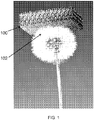
- a metallic micro-lattice was fabricated according to the present invention with a periodic architecture of hollow tubes that connect at nodes, forming an octahedral unit cell (as shown in FIG. 1 ).
- the architecture and the fabrication process provided for a wall thickness of the hollow tubes as thin as 100 nm, resulting in a cellular material with a density of 0.9 mg/cm 3 .
- the density is calculated using the weight of the solid structures, but not including the weight of the air in the pores, adhering to standard practice for cellular materials, The density of air at ambient conditions, 1.2 mg/cm 3 , would need to be added to express the density of the solid-air composite.
- the present invention provides for an ultra-light cellular material having a relative density in a range of 0,001% to 0.3%.
- the relative density is the ratio of the density (mass of a unit volume) of a substance or object to the density of a given reference material in this case the constituent material which comprises the micro-lattice (such as the hollow tubes).
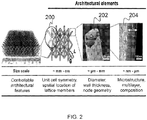
- FIG. 2 illustrates how the micro-lattice architecture can be distilled into three levels of hierarchy at three distinct length scales: unit cell ( ⁇ mm - cm) 200, hollow tube lattice member ( ⁇ m - mm) 202 (i.e., hollow tubes or struts) and hollow tube wall ( ⁇ nm - ⁇ m) 204.
- unit cell ⁇ mm - cm
- hollow tube lattice member ⁇ m - mm
- hollow tube wall ⁇ nm - ⁇ m
- unit cell size and topology, hollow tube diameter and wall thickness can be altered independently; when combined with conformal thin-film coating methods, micro-lattice structures with a wide range of constituent compositions and micro-structures become available.
- the architecture determines the relative density of the lattice, and the film material then dictates the absolute density.
- the extraordinary control over architecture facilitates de-coupling historically linked properties - like density and stiffness - by allowing independent tailoring of specific properties.
- the compressive modulus of these micro-lattices can be altered by modifying the inclination angle without changing the density significantly (See Literature Reference No. 11).
- the method to design the micro-lattice architecture at multiple scales from nm to cm allows significantly more control than typical methods for forming ultra-lightweight materials, especially foams and aerogels, where nominally random processes govern porosity formation.
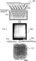
- the micro-lattice templates were fabricated using a self-propagating photopolymer waveguide technique reported previously (See Literature Reference No. 12), whereby a suitable liquid photomonomer 300 is exposed to collimated UV light 302 through a patterned mask 304, producing an interconnected three-dimensional photopolymer lattice 306.
- a suitable liquid photomonomer 300 is a thiol-ene resin.
- architectures can be generated with 1 - 4 mm lattice member length L , 100-500 ⁇ m lattice member diameter D , 100-500 nm wall thickness t , and 60° inclination angle ⁇ , similar to the micro-lattices depicted in FIG. 2 .
- the polymer lattice 306 is an open cellular templates. After the polymer lattice 306 is generated, films (e.g., conformal nickel-phosphorous thin films) were deposited on the polymer lattices 306 by electroless plating 308 and the polymer was subsequently etched out 310 (via chemical etching or any other suitable etching technique that is gentle enough not to destroy the micro-lattice).
- the etchant has to be selective with respect to the template and the coating material i.e.. the etching rate of the template needs to be substantially faster than that of the coating.
- sodium hydroxide solution is the preferred etchant, for other material combinations, organic solvents, plasma etching, thermal pyrolysis or other erchants are favored. Freeze drying is used for fragile micro-lattices that are deformed by capillary forces on removal from solution.
- the auto-catalytic electroless nickel plating reaction enables deposition of thin films with controlled thickness on complex shapes and inside pores without noticeable mass transport limitations.
- a wall thickness of 100 nm can be achieved while maintaining a uniform conformal coating.
- the resulting ultra-light micro-lattice 312 essentially translates the deposited nano-scale thin film in three dimensions to form a macroscopic material where the base structural elements are hollow tubes (as shown in FIG. 2 ).
- any suitable material can be deposited on the polymer lattice 306, non-limiting examples of which include nickel zinc, chrome, tin, copper, gold silver, platinum, rhodium, aluminum, a ceramic, including, diamond, diamond like carbon, alumina, zirconia, tin oxide, zinc oxide, silicon carbide, silicon nitride, titanium nitride, tantalum nitride, tungsten nitride, a polymer including parylene or combinations or alloys thereof including multi-layers of different Materials.
- Micro-lattices with these extreme low densities exhibit unique mechanical behavior. Compression experiments on micro-lattices show recovery from strains exceeding 50%.
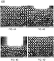
- FIG. 4C shows the micro-lattice at 50% compression.
- the stress drops rapidly but does not approach zero until the platen is close to its original position.
- the micro-lattice recovers to 98,6% of its original height and resumes its original shape (as shown in FIG. 4D ).
- FIGs. 4E through 4H provide images of the micro-lattice sample through its compression and recovery. More specifically, FIG.
- FIG. 4E is an optical image of a unit cell of the micro-lattice, in an unloaded or uncompressed condition.
- FIG. 4F is an optical image of the unit cell, depicting how the unit cell accommodates compressive strain by buckling at the nodes.
- FIG. 4G is a scanning electron microscopy (SEM) image of a node before testing, while FIG. 4H is an SEM image of the node after six compression cycles at 50% strain.
- SEM scanning electron microscopy
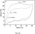
- FIG. 5C shows the stress-strain curves of the first two compression cycles of a sample with a density of 1 mg/cm 3 and larger unit cells (L: 4 mm, D: 500 ⁇ m, t:120 nm) illustrating similar behavior of different micro-lattices in the ultra-low density regime. Increasing the density and wall thickness will eventuallv lead to compression behavior more typical for metallic cellular materials.
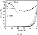
- FIG. 5D shows the compression of a sample with 43mg/cc (L: 1050 ⁇ m, D: 150 ⁇ m, t: 1400 nm): notice that strain recovery upon unloading from 50% strain is essentially absent.
- the bulk micro-lattice material can undergo large compressive strains without enduring further fracture or plastic deformation in the solid nickel-phosphorous material, thus exhibiting the reversible compressive behavior shown in FIGs. 4A through 5D .
- the extremely small aspect ratio of the hollow tube wall to diameter plays a key role in the nearly fall recoverability, by allowing truss members to undergo large rotations about regnant nodal ligaments without accumulation of significant plasticity. Increasing this aspect ratio leads to excessive fracture and loss of the recoverable deformation behavior (as shown in FIG. 5D ).
- the micro-lattices exhibit completely different bulk properties: the cellular architecture effectively transforms the brittle thin-film property into a ductile and super-elastic lattice behavior by enabling sufficient freedom for deformation and tolerance to local strains, such as forming relief cracks that are stable during repeated compression cycles, while still maintaining the structure to remain coherent.
- cellular material architecture can fundamentally change the material properties and generate functional ductility and functional superelasticity at the bulk scale.
- micro-lattice materials with even lower density could be fabricated by following the same methodology.
- the wall thickness t reaches a minimum at 100 nm with the current fabrication process because it requires a continuous and robust film that can withstand the mechanical forces associated with removal of the polymer template.
- the density decreases with increasing cell size, or lattice member length L.
- the density could be pushed lower with a constituent thin film material with a higher specific stiffness and strength.
- Diamond may be among the best candidates with its extremely high stiffness and strength and well established vapor deposition routes enabling films with ⁇ 50 nm thickness (See Literature Reference No. 20).
- Polymer micro-lattice templates were fabricated from an interconnected pattern of self-propagating photopolymer waveguides as described in detail elsewhere (See Literature Reference Nos. 12 and 13). Prior to electroless plating, all samples were thermally post-cured at 120°C in air for 12 hrs.
- the polymer micro-lattice template samples were then used as direct templates for electroless nickel plating using a commercially available process, such as that provided by OM Group Inc., located at 127 Public Square, 1500 Key Tower, Cleveland, Ohio 44114.
- OM Group Inc. located at 127 Public Square, 1500 Key Tower, Cleveland, Ohio 44114.
- the polymer sample were first heat treated at greater than 120 degrees Celsius and then immersed in 1 molar sodium hydroxide solution, then palladium catalyst was deposited by immersion in activator solution containing hydrochloric acid and tin(II) chloride (Fidelity 1018, OM Group Inc.), followed by an etch in accelerator solution containing fluoboric acid (Fidelity 1019, OM Group Inc.).
- the samples were then immersed in electroless nickel plating solution with nickel sulfate as nickel source, sodium hypophosphite as reducing agent, and sodium malate and acetic acid as complexing agents (9026M, OM Group Inc.).
- the electroless nickel plating bath was kept at pH 4.9 by addition of ammonium hydroxide and plating was performed at 80°C. Different plating times were chosen to achieve different coating thicknesses (as reported in FIG. 6 ).
- a wall thickness / of 500 nm was achieved by electroless nickel plating of approximately 3 minutes, After nickel deposition the top and bottom surface of each sample was sanded to expose the underlying polymer at each node.
- the polymer was then chemically etched in a base solution (3M NaOH at 60°C) for 24 hours, creating the hollow tube nickel micro-lattice samples in FIG. 2 .
- Samples with wall thickness below -150 nm could not be removed from the aqueous NaOH solution directly because the capillary forces deformed the lattice. In these cases, the samples where freeze dried after exchanging the NaOH solution to deionized water and then to t-butanol.
- the conditions during the chemical etch have to be carefully adjusted to provide enough agitation to dissolve the polymer in the hollow tubes but limit the forces acting on the micro-lattice to avoid fracture.
- Successful etching conditions were achieved by inserting shields around the micro-lattice to protect it from the solution flow, below a certain wall thickness, depending on the architecture, the micro-lattice is too fragile to remove them from the liquid. In this case freeze drying is employed to remove the liquid.
- a solvent exchange was performed to exchange the aqueous NaOH solution with t-Butanol and subsequently the t-Butanol containing the micro-lattice is frozen. T-Butanol exhibits a much lower volume change on freezing than water resulting in less damage to the microlattice.
- a vacuum is then applied to sublimate the t-butanol leaving a dry micro-lattice of the present invention behind.
Landscapes
- Chemical & Material Sciences (AREA)
- Engineering & Computer Science (AREA)
- Organic Chemistry (AREA)
- Materials Engineering (AREA)
- Metallurgy (AREA)
- Mechanical Engineering (AREA)
- Chemical Kinetics & Catalysis (AREA)
- General Chemical & Material Sciences (AREA)
- Ceramic Engineering (AREA)
- Manufacturing & Machinery (AREA)
- Structural Engineering (AREA)
- Microelectronics & Electronic Packaging (AREA)
- Analytical Chemistry (AREA)
- Inorganic Chemistry (AREA)
- Physics & Mathematics (AREA)
- General Physics & Mathematics (AREA)
- Micromachines (AREA)
- Chemically Coating (AREA)
- Chemical Vapour Deposition (AREA)
- Laminated Bodies (AREA)
- Physical Or Chemical Processes And Apparatus (AREA)
Claims (12)
- Mikrogitter umfassend:Zellmaterial, gebildet aus einer Vielzahl von sich überkreuzenden hohlen Röhren, wobei das Zellmaterial eine relative Dichte in einem Bereich von 0,001% bis 0,3% im Verhältnis zur theoretischen Dichte des Materials aufweist;wobei die hohlen Röhren einen Durchmesser derart aufweisen, dass der Durchmesser zwischen 10 und 1000 µm ist; undwobei die hohlen Röhren durch Röhrenwände ausgebildet sind, die eine Wanddicke zwischen 0,01 und 2 µm aufweisen.
- Mikrogitter nach Anspruch 1, wobei die hohlen Röhren durch Röhrenwände mit einer Wanddicke von zwischen 0,1 und 1 µm ausgebildet sind.
- Mikrogitter nach Anspruch 1, wobei das Zellmaterial geeignet ist, sich von Verformungen in einem Bereich von 2% bis 90% zu regenerieren.
- Verfahren zur Bildung eines Mikrogitters, umfassend die folgenden Schritte:Bilden einer Mikrogittervorlage;Überziehen der Mikrogittervorlage mit einem Materialfilm;Entfernen der Mikrogittervorlage, um ein Zellmaterial, das aus einer Vielzahl von sich überkreuzenden hohlen Röhren besteht, zu geben, wobei das Zellmaterial eine relative Dichte im Bereich von 0,001% bis 0,3% im Verhältnis zur theoretischen Dichte des Materials aufweist;wobei die hohlen Röhren einen Durchmesser derart aufweisen, dass der Durchmesser zwischen 10 und 1000 µm ist; undwobei die hohlen Röhren durch Röhrenwände mit einer Wanddicke von zwischen 0,01 und 2 µm ausgebildet sind.
- Verfahren nach Anspruch 4, wobei die Mikrogittervorlage durch Exponieren eines Photomonomers gegenüber einem gebündelten UV-Licht durch eine fein strukturierte Membran ausgebildet ist.
- Verfahren nach Anspruch 5, wobei die Mikrogittervorlage ein miteinander verbundenes dreidimensionales offenes zelluläres Photopolymergitter ist.
- Verfahren nach Anspruch 6, wobei die Mikrogittervorlage beim Beschichten mit einem Materialfilm überzogen wird, wobei der Materialfilm ein Metall, Keramik oder Polymer ist.
- Verfahren nach Anspruch 7, wobei beim Entfernen der Mikrogittervorlage chemisches Ätzen beim Entfernen der Mikrogittervorlage angewendet wird.
- Verfahren nach Anspruch 4, wobei die Mikrogittervorlage beim Beschichten mit einem Materialfilm überzogen wird, wobei die Mikrogittervorlage unter Verwendung einer Technik, ausgewählt aus der Gruppe bestehend aus Galvanik, elektrophoretischer Ablagerung, chemischer Beschichtung aus der Gasphase, physikalischer Gasphasenabscheidung, Atomlagenabscheidung, Lösungsabscheidung oder Sol-Gel-Abscheidung, beschichtet wird.
- Verfahren nach Anspruch 4, wobei die Mikrogittervorlage ein miteinander verbundenes dreidimensionales offenes zelluläres Photopolymergitter ist.
- Verfahren nach Anspruch 4, wobei die Mikrogittervorlage beim Beschichten mit einem Materialfilm überzogen wird, wobei der Materialfilm ein Metall, Keramik oder Polymer ist.
- Mikrogitter nach Anspruch 1, wobei die hohlen Röhren aus einem Material, augewählt aus der Gruppe bestehend aus Nickel, Zink, Chrom, Zinn, Kupfer, Gold Silber, Platin, Rhodium, Aluminium, einer Keramik, einschließlich Diamant, diamantähnlichem Kohlenstoff, Aluminiumoxid, Zirconium, Zinnoxid, Zinkoxid, Siliziumoxid, Siliziumkarbid, Siliziumnitrid, Titaniumnitrid, Tantalumnitrid, Wolfram-Nitrid, einem Polymer einschließlich Parylen, oder einer Kombination oder Legierung davon, gebildet sind.
Priority Applications (1)
| Application Number | Priority Date | Filing Date | Title |
|---|---|---|---|
| EP17170005.7A EP3263518B1 (de) | 2011-08-17 | 2012-08-15 | Ultraleichte mikrogitter und verfahren zu deren herstellung |
Applications Claiming Priority (3)
| Application Number | Priority Date | Filing Date | Title |
|---|---|---|---|
| US201161524714P | 2011-08-17 | 2011-08-17 | |
| US13/584,108 US9415562B1 (en) | 2011-08-17 | 2012-08-13 | Ultra-light micro-lattices and a method for forming the same |
| PCT/US2012/050936 WO2013025800A2 (en) | 2011-08-17 | 2012-08-15 | Ultra-light micro-lattices and a method for forming the same |
Related Child Applications (1)
| Application Number | Title | Priority Date | Filing Date |
|---|---|---|---|
| EP17170005.7A Division EP3263518B1 (de) | 2011-08-17 | 2012-08-15 | Ultraleichte mikrogitter und verfahren zu deren herstellung |
Publications (3)
| Publication Number | Publication Date |
|---|---|
| EP2744744A2 EP2744744A2 (de) | 2014-06-25 |
| EP2744744A4 EP2744744A4 (de) | 2015-03-25 |
| EP2744744B1 true EP2744744B1 (de) | 2017-05-10 |
Family
ID=47715682
Family Applications (2)
| Application Number | Title | Priority Date | Filing Date |
|---|---|---|---|
| EP12823315.2A Active EP2744744B1 (de) | 2011-08-17 | 2012-08-15 | Ultraleichte mikrogitter und verfahren zu ihrer herstellung |
| EP17170005.7A Active EP3263518B1 (de) | 2011-08-17 | 2012-08-15 | Ultraleichte mikrogitter und verfahren zu deren herstellung |
Family Applications After (1)
| Application Number | Title | Priority Date | Filing Date |
|---|---|---|---|
| EP17170005.7A Active EP3263518B1 (de) | 2011-08-17 | 2012-08-15 | Ultraleichte mikrogitter und verfahren zu deren herstellung |
Country Status (4)
| Country | Link |
|---|---|
| US (2) | US9415562B1 (de) |
| EP (2) | EP2744744B1 (de) |
| CN (1) | CN103958392B (de) |
| WO (1) | WO2013025800A2 (de) |
Families Citing this family (23)
| Publication number | Priority date | Publication date | Assignee | Title |
|---|---|---|---|---|
| US10119589B2 (en) | 2011-08-17 | 2018-11-06 | Hrl Laboratories, Llc | Microlattice damping material and method for repeatable energy absorption |
| US9527261B1 (en) * | 2012-09-14 | 2016-12-27 | Hrl Laboratories, Llc | Hollow polymer micro-truss structures containing pressurized fluids |
| EP2946127A4 (de) * | 2013-01-17 | 2016-07-20 | Hrl Lab Llc | Mikrogitter-dämpfungsmaterial und verfahren zur wiederholbaren energieabsorption |
| US9405067B2 (en) | 2013-03-13 | 2016-08-02 | Hrl Laboratories, Llc | Micro-truss materials having in-plane material property variations |
| US9590228B1 (en) | 2013-11-01 | 2017-03-07 | HRL Laboratroies, LLC | Three-dimensional micro-lattice battery structures with convective flow of electrolytes |
| US9925440B2 (en) * | 2014-05-13 | 2018-03-27 | Bauer Hockey, Llc | Sporting goods including microlattice structures |
| US10427336B2 (en) | 2014-11-20 | 2019-10-01 | Baker Hughes, A Ge Company, Llc | Periodic structured composite and articles therefrom |
| WO2017173396A1 (en) * | 2016-03-31 | 2017-10-05 | The Regents Of The University Of California | Composite foam |
| US10034519B2 (en) | 2016-06-16 | 2018-07-31 | Adidas Ag | UV curable lattice microstructure for footwear |
| US10611278B2 (en) * | 2017-11-29 | 2020-04-07 | B/E Aerospace, Inc. | Lattices for use in aircraft seat assemblies |
| US11254775B2 (en) | 2017-12-28 | 2022-02-22 | Texas Instruments Incorporated | Filler particles for polymers |
| US11938715B2 (en) | 2017-12-28 | 2024-03-26 | Texas Instruments Incorporated | SP2-bonded carbon structures |
| US11390527B2 (en) | 2017-12-28 | 2022-07-19 | Texas Instruments Incorporated | Multi-layered SP2-bonded carbon tubes |
| US11370662B2 (en) * | 2017-12-28 | 2022-06-28 | Texas Instruments Incorporated | Hexagonal boron nitride structures |
| US11267920B2 (en) | 2018-02-02 | 2022-03-08 | Triad National Security, Llc | Hierarchical printed product and composition and method for making the same |
| FR3077814B1 (fr) * | 2018-02-09 | 2020-03-13 | Commissariat A L'energie Atomique Et Aux Energies Alternatives | Structure metallique et/ou ceramique en micro-treillis et son procede de fabrication |
| US11318435B2 (en) | 2018-09-21 | 2022-05-03 | California Institute Of Technology | 3D printing of metal containing structures |
| US10748999B2 (en) | 2018-12-21 | 2020-08-18 | Texas Instruments Incorporated | Multi-super lattice for switchable arrays |
| CA3140503C (en) | 2019-05-21 | 2022-06-14 | Bauer Hockey Ltd. | Helmets comprising additively-manufactured components |
| CN111056846B (zh) * | 2019-12-06 | 2021-04-20 | 西安交通大学 | 一种采用冷冻干燥和燃烧合成法快速制备的定向多孔氮化铝蜂窝陶瓷及其方法 |
| CN113806989B (zh) * | 2021-09-30 | 2024-05-07 | 喜临门家具股份有限公司 | 沙发座面弹性材料的应力应变关系的有限元分析方法 |
| CN115312017A (zh) * | 2022-08-12 | 2022-11-08 | 江苏省声学产业技术创新中心 | 一种超轻的吸声材料 |
| CN116024619B (zh) * | 2022-11-25 | 2024-11-15 | 梧州三和新材料科技有限公司 | 具有敞开式骨架的多孔金属及其制造方法 |
Family Cites Families (25)
| Publication number | Priority date | Publication date | Assignee | Title |
|---|---|---|---|---|
| US3694325A (en) * | 1971-06-21 | 1972-09-26 | Gen Motors Corp | Process for uniformly electroforming intricate three-dimensional substrates |
| US4053371A (en) * | 1976-06-01 | 1977-10-11 | The Dow Chemical Company | Cellular metal by electrolysis |
| US4390599A (en) * | 1980-07-31 | 1983-06-28 | Raychem Corporation | Enhanced recovery memory metal device |
| FR2558485B1 (fr) * | 1984-01-25 | 1990-07-13 | Rech Applic Electrochimique | Structure metallique poreuse, son procede de fabrication et applications |
| US4752498A (en) * | 1987-03-02 | 1988-06-21 | Fudim Efrem V | Method and apparatus for production of three-dimensional objects by photosolidification |
| US5109589A (en) * | 1991-03-11 | 1992-05-05 | United Technologies Corporation | Processes for making metal prototype parts |
| CA2221195A1 (en) * | 1997-11-14 | 1999-05-14 | Chantal E. Holy | Biodegradable polymer matrix |
| US6472210B1 (en) * | 1997-11-14 | 2002-10-29 | Bonetec Corporation | Polymer scaffold having microporous polymer struts defining interconnected macropores |
| US7022522B2 (en) * | 1998-11-13 | 2006-04-04 | Limin Guan | Macroporous polymer scaffold containing calcium phosphate particles |
| US6503564B1 (en) * | 1999-02-26 | 2003-01-07 | 3M Innovative Properties Company | Method of coating microstructured substrates with polymeric layer(s), allowing preservation of surface feature profile |
| DE60138627D1 (de) * | 2000-07-14 | 2009-06-18 | Univ Virginia | Schaum für wärmetauscher |
| MXPA03000732A (es) * | 2000-07-28 | 2003-07-14 | Univ Brigham Young | Estructura armada isometrica. |
| NL1016779C2 (nl) * | 2000-12-02 | 2002-06-04 | Cornelis Johannes Maria V Rijn | Matrijs, werkwijze voor het vervaardigen van precisieproducten met behulp van een matrijs, alsmede precisieproducten, in het bijzonder microzeven en membraanfilters, vervaardigd met een dergelijke matrijs. |
| AU2002322041A1 (en) | 2001-06-06 | 2002-12-16 | University Of Virginia Patent Foundation | Multifunctional periodic cellular solids and the method of making the same |
| KR100441376B1 (ko) * | 2002-01-31 | 2004-07-23 | (주)퓨얼셀 파워 | 얇은 두께를 갖는 콤포지트 멤브레인 |
| US6930053B2 (en) | 2002-03-25 | 2005-08-16 | Sanyo Electric Co., Ltd. | Method of forming grating microstructures by anodic oxidation |
| WO2004011245A1 (en) * | 2002-07-25 | 2004-02-05 | University Of Virginia Patent Foundation | Method for manufacture of cellular materials and structures for blast and impact mitigation and resulting structure |
| US7627938B2 (en) | 2004-10-15 | 2009-12-08 | Board Of Regents, The Univeristy Of Texas System | Tapered hollow metallic microneedle array assembly and method of making and using the same |
| US7704644B2 (en) * | 2005-01-25 | 2010-04-27 | University Of Delaware | Zero-alignment method for tunable fabrication of three-dimensional photonic crystals by multiple-exposure laser interference using diffraction gratings patterned on a single mask |
| US7736724B1 (en) * | 2005-05-13 | 2010-06-15 | The University Of Tulsa | Fabrication of nanobaskets by sputter deposition on porous substrates and uses thereof |
| US7421159B2 (en) * | 2005-12-13 | 2008-09-02 | Board of Supervisor of Louisiana State University and Agricultural and Mechanical College | Integral pre-aligned micro-optical systems |
| US7687132B1 (en) * | 2008-03-05 | 2010-03-30 | Hrl Laboratories, Llc | Ceramic microtruss |
| US7382959B1 (en) * | 2006-10-13 | 2008-06-03 | Hrl Laboratories, Llc | Optically oriented three-dimensional polymer microstructures |
| US7653276B1 (en) * | 2008-03-06 | 2010-01-26 | Hrl Laboratories, Llc | Composite structures for storing thermal energy |
| US8268510B2 (en) * | 2008-12-22 | 2012-09-18 | GM Global Technology Operations LLC | Fuel cell fabrication using photopolymer based processes |
-
2012
- 2012-08-13 US US13/584,108 patent/US9415562B1/en not_active Expired - Fee Related
- 2012-08-15 WO PCT/US2012/050936 patent/WO2013025800A2/en not_active Ceased
- 2012-08-15 CN CN201280040063.9A patent/CN103958392B/zh active Active
- 2012-08-15 EP EP12823315.2A patent/EP2744744B1/de active Active
- 2012-08-15 EP EP17170005.7A patent/EP3263518B1/de active Active
-
2016
- 2016-07-01 US US15/201,344 patent/US9938623B1/en not_active Expired - Fee Related
Also Published As
| Publication number | Publication date |
|---|---|
| EP2744744A2 (de) | 2014-06-25 |
| US9415562B1 (en) | 2016-08-16 |
| EP2744744A4 (de) | 2015-03-25 |
| EP3263518B1 (de) | 2021-04-07 |
| WO2013025800A2 (en) | 2013-02-21 |
| EP3263518A1 (de) | 2018-01-03 |
| US9938623B1 (en) | 2018-04-10 |
| CN103958392B (zh) | 2019-03-08 |
| CN103958392A (zh) | 2014-07-30 |
| WO2013025800A3 (en) | 2013-04-25 |
Similar Documents
| Publication | Publication Date | Title |
|---|---|---|
| EP2744744B1 (de) | Ultraleichte mikrogitter und verfahren zu ihrer herstellung | |
| Torrents et al. | Characterization of nickel-based microlattice materials with structural hierarchy from the nanometer to the millimeter scale | |
| Wang et al. | Synthesis of mesoporous Pt films with tunable pore sizes from aqueous surfactant solutions | |
| Song et al. | Topology optimization-guided lattice composites and their mechanical characterizations | |
| Schaedler et al. | Ultralight metallic microlattices | |
| Mieszala et al. | Micromechanics of amorphous metal/polymer hybrid structures with 3D cellular architectures: size effects, buckling behavior, and energy absorption capability | |
| US10119589B2 (en) | Microlattice damping material and method for repeatable energy absorption | |
| Gu et al. | Ultra-strong architected Cu meso-lattices | |
| Jiao et al. | Tunable nanoporous metallic glasses fabricated by selective phase dissolution and passivation for ultrafast hydrogen uptake | |
| Hakamada et al. | Hydrogen storage properties of nanoporous palladium fabricated by dealloying | |
| Kim et al. | Breaking the elastic limit of piezoelectric ceramics using nanostructures: A case study using ZnO | |
| EP4052817B1 (de) | Hoch schmelzpunkt kelvin struktur gitter metall, herstellungsverfahren und seine anwendung | |
| US11938545B2 (en) | Ultralight conductive metallic aerogels | |
| Biener et al. | Ultra‐strong and low‐density nanotubular bulk materials with tunable feature sizes | |
| US8715781B2 (en) | Nanoporous coating synthesis and apparatus | |
| Li et al. | Durable and flexible hydrophobic surface with a micropatterned composite metal–polymer structure | |
| CN105008759B (zh) | 微晶格阻尼材料和可重复吸收能量的方法 | |
| CN107572476B (zh) | 一种制备金属微纳米结构的方法 | |
| Ramachandramoorthy et al. | Dual-templated electrodeposition and characterization of regular metallic foam based microarchitectures | |
| Lian et al. | Catastrophic vs gradual collapse of thin-walled nanocrystalline Ni hollow cylinders as building blocks of microlattice structures | |
| Sadek et al. | Bioinspired nanonetwork hydroxyapatite from block copolymer templated synthesis for mechanical metamaterials | |
| CN108018531A (zh) | 一种制备纳米多孔金属材料的方法 | |
| Kang et al. | Molecular mechanics of Ag nanowire transfer processes subjected to contact loading by a PDMS substrate | |
| Li et al. | Interface feature characterization and Schottky interfacial layer confirmation of TiO2 nanotube array film | |
| Carpena-Núñez et al. | Mechanical characterization of pristine and hydrogen-exposed palladium nanowires by in situ TEM |
Legal Events
| Date | Code | Title | Description |
|---|---|---|---|
| PUAI | Public reference made under article 153(3) epc to a published international application that has entered the european phase |
Free format text: ORIGINAL CODE: 0009012 |
|
| 17P | Request for examination filed |
Effective date: 20140314 |
|
| AK | Designated contracting states |
Kind code of ref document: A2 Designated state(s): AL AT BE BG CH CY CZ DE DK EE ES FI FR GB GR HR HU IE IS IT LI LT LU LV MC MK MT NL NO PL PT RO RS SE SI SK SM TR |
|
| DAX | Request for extension of the european patent (deleted) | ||
| REG | Reference to a national code |
Ref country code: DE Ref legal event code: R079 Ref document number: 602012032358 Country of ref document: DE Free format text: PREVIOUS MAIN CLASS: B81B0001000000 Ipc: B81C0001000000 |
|
| A4 | Supplementary search report drawn up and despatched |
Effective date: 20150220 |
|
| RIC1 | Information provided on ipc code assigned before grant |
Ipc: C04B 38/00 20060101ALI20150216BHEP Ipc: B81C 1/00 20060101AFI20150216BHEP |
|
| GRAP | Despatch of communication of intention to grant a patent |
Free format text: ORIGINAL CODE: EPIDOSNIGR1 |
|
| INTG | Intention to grant announced |
Effective date: 20161125 |
|
| GRAS | Grant fee paid |
Free format text: ORIGINAL CODE: EPIDOSNIGR3 |
|
| GRAA | (expected) grant |
Free format text: ORIGINAL CODE: 0009210 |
|
| AK | Designated contracting states |
Kind code of ref document: B1 Designated state(s): AL AT BE BG CH CY CZ DE DK EE ES FI FR GB GR HR HU IE IS IT LI LT LU LV MC MK MT NL NO PL PT RO RS SE SI SK SM TR |
|
| REG | Reference to a national code |
Ref country code: GB Ref legal event code: FG4D |
|
| REG | Reference to a national code |
Ref country code: AT Ref legal event code: REF Ref document number: 892107 Country of ref document: AT Kind code of ref document: T Effective date: 20170515 Ref country code: CH Ref legal event code: EP |
|
| REG | Reference to a national code |
Ref country code: IE Ref legal event code: FG4D |
|
| REG | Reference to a national code |
Ref country code: DE Ref legal event code: R096 Ref document number: 602012032358 Country of ref document: DE |
|
| REG | Reference to a national code |
Ref country code: NL Ref legal event code: MP Effective date: 20170510 |
|
| REG | Reference to a national code |
Ref country code: LT Ref legal event code: MG4D |
|
| REG | Reference to a national code |
Ref country code: AT Ref legal event code: MK05 Ref document number: 892107 Country of ref document: AT Kind code of ref document: T Effective date: 20170510 |
|
| PG25 | Lapsed in a contracting state [announced via postgrant information from national office to epo] |
Ref country code: HR Free format text: LAPSE BECAUSE OF FAILURE TO SUBMIT A TRANSLATION OF THE DESCRIPTION OR TO PAY THE FEE WITHIN THE PRESCRIBED TIME-LIMIT Effective date: 20170510 Ref country code: LT Free format text: LAPSE BECAUSE OF FAILURE TO SUBMIT A TRANSLATION OF THE DESCRIPTION OR TO PAY THE FEE WITHIN THE PRESCRIBED TIME-LIMIT Effective date: 20170510 Ref country code: AT Free format text: LAPSE BECAUSE OF FAILURE TO SUBMIT A TRANSLATION OF THE DESCRIPTION OR TO PAY THE FEE WITHIN THE PRESCRIBED TIME-LIMIT Effective date: 20170510 Ref country code: FI Free format text: LAPSE BECAUSE OF FAILURE TO SUBMIT A TRANSLATION OF THE DESCRIPTION OR TO PAY THE FEE WITHIN THE PRESCRIBED TIME-LIMIT Effective date: 20170510 Ref country code: ES Free format text: LAPSE BECAUSE OF FAILURE TO SUBMIT A TRANSLATION OF THE DESCRIPTION OR TO PAY THE FEE WITHIN THE PRESCRIBED TIME-LIMIT Effective date: 20170510 Ref country code: NO Free format text: LAPSE BECAUSE OF FAILURE TO SUBMIT A TRANSLATION OF THE DESCRIPTION OR TO PAY THE FEE WITHIN THE PRESCRIBED TIME-LIMIT Effective date: 20170810 Ref country code: GR Free format text: LAPSE BECAUSE OF FAILURE TO SUBMIT A TRANSLATION OF THE DESCRIPTION OR TO PAY THE FEE WITHIN THE PRESCRIBED TIME-LIMIT Effective date: 20170811 |
|
| PG25 | Lapsed in a contracting state [announced via postgrant information from national office to epo] |
Ref country code: PL Free format text: LAPSE BECAUSE OF FAILURE TO SUBMIT A TRANSLATION OF THE DESCRIPTION OR TO PAY THE FEE WITHIN THE PRESCRIBED TIME-LIMIT Effective date: 20170510 Ref country code: BG Free format text: LAPSE BECAUSE OF FAILURE TO SUBMIT A TRANSLATION OF THE DESCRIPTION OR TO PAY THE FEE WITHIN THE PRESCRIBED TIME-LIMIT Effective date: 20170810 Ref country code: RS Free format text: LAPSE BECAUSE OF FAILURE TO SUBMIT A TRANSLATION OF THE DESCRIPTION OR TO PAY THE FEE WITHIN THE PRESCRIBED TIME-LIMIT Effective date: 20170510 Ref country code: LV Free format text: LAPSE BECAUSE OF FAILURE TO SUBMIT A TRANSLATION OF THE DESCRIPTION OR TO PAY THE FEE WITHIN THE PRESCRIBED TIME-LIMIT Effective date: 20170510 Ref country code: IS Free format text: LAPSE BECAUSE OF FAILURE TO SUBMIT A TRANSLATION OF THE DESCRIPTION OR TO PAY THE FEE WITHIN THE PRESCRIBED TIME-LIMIT Effective date: 20170910 Ref country code: SE Free format text: LAPSE BECAUSE OF FAILURE TO SUBMIT A TRANSLATION OF THE DESCRIPTION OR TO PAY THE FEE WITHIN THE PRESCRIBED TIME-LIMIT Effective date: 20170510 Ref country code: NL Free format text: LAPSE BECAUSE OF FAILURE TO SUBMIT A TRANSLATION OF THE DESCRIPTION OR TO PAY THE FEE WITHIN THE PRESCRIBED TIME-LIMIT Effective date: 20170510 |
|
| PG25 | Lapsed in a contracting state [announced via postgrant information from national office to epo] |
Ref country code: CZ Free format text: LAPSE BECAUSE OF FAILURE TO SUBMIT A TRANSLATION OF THE DESCRIPTION OR TO PAY THE FEE WITHIN THE PRESCRIBED TIME-LIMIT Effective date: 20170510 Ref country code: EE Free format text: LAPSE BECAUSE OF FAILURE TO SUBMIT A TRANSLATION OF THE DESCRIPTION OR TO PAY THE FEE WITHIN THE PRESCRIBED TIME-LIMIT Effective date: 20170510 Ref country code: SK Free format text: LAPSE BECAUSE OF FAILURE TO SUBMIT A TRANSLATION OF THE DESCRIPTION OR TO PAY THE FEE WITHIN THE PRESCRIBED TIME-LIMIT Effective date: 20170510 Ref country code: RO Free format text: LAPSE BECAUSE OF FAILURE TO SUBMIT A TRANSLATION OF THE DESCRIPTION OR TO PAY THE FEE WITHIN THE PRESCRIBED TIME-LIMIT Effective date: 20170510 Ref country code: DK Free format text: LAPSE BECAUSE OF FAILURE TO SUBMIT A TRANSLATION OF THE DESCRIPTION OR TO PAY THE FEE WITHIN THE PRESCRIBED TIME-LIMIT Effective date: 20170510 |
|
| REG | Reference to a national code |
Ref country code: DE Ref legal event code: R097 Ref document number: 602012032358 Country of ref document: DE |
|
| PG25 | Lapsed in a contracting state [announced via postgrant information from national office to epo] |
Ref country code: IT Free format text: LAPSE BECAUSE OF FAILURE TO SUBMIT A TRANSLATION OF THE DESCRIPTION OR TO PAY THE FEE WITHIN THE PRESCRIBED TIME-LIMIT Effective date: 20170510 Ref country code: SM Free format text: LAPSE BECAUSE OF FAILURE TO SUBMIT A TRANSLATION OF THE DESCRIPTION OR TO PAY THE FEE WITHIN THE PRESCRIBED TIME-LIMIT Effective date: 20170510 |
|
| PLBE | No opposition filed within time limit |
Free format text: ORIGINAL CODE: 0009261 |
|
| STAA | Information on the status of an ep patent application or granted ep patent |
Free format text: STATUS: NO OPPOSITION FILED WITHIN TIME LIMIT |
|
| REG | Reference to a national code |
Ref country code: CH Ref legal event code: PL |
|
| PG25 | Lapsed in a contracting state [announced via postgrant information from national office to epo] |
Ref country code: MC Free format text: LAPSE BECAUSE OF FAILURE TO SUBMIT A TRANSLATION OF THE DESCRIPTION OR TO PAY THE FEE WITHIN THE PRESCRIBED TIME-LIMIT Effective date: 20170510 |
|
| 26N | No opposition filed |
Effective date: 20180213 |
|
| GBPC | Gb: european patent ceased through non-payment of renewal fee |
Effective date: 20170815 |
|
| PG25 | Lapsed in a contracting state [announced via postgrant information from national office to epo] |
Ref country code: CH Free format text: LAPSE BECAUSE OF NON-PAYMENT OF DUE FEES Effective date: 20170831 Ref country code: LI Free format text: LAPSE BECAUSE OF NON-PAYMENT OF DUE FEES Effective date: 20170831 |
|
| REG | Reference to a national code |
Ref country code: FR Ref legal event code: ST Effective date: 20180430 |
|
| REG | Reference to a national code |
Ref country code: IE Ref legal event code: MM4A |
|
| PG25 | Lapsed in a contracting state [announced via postgrant information from national office to epo] |
Ref country code: SI Free format text: LAPSE BECAUSE OF FAILURE TO SUBMIT A TRANSLATION OF THE DESCRIPTION OR TO PAY THE FEE WITHIN THE PRESCRIBED TIME-LIMIT Effective date: 20170510 |
|
| REG | Reference to a national code |
Ref country code: BE Ref legal event code: MM Effective date: 20170831 |
|
| PG25 | Lapsed in a contracting state [announced via postgrant information from national office to epo] |
Ref country code: LU Free format text: LAPSE BECAUSE OF NON-PAYMENT OF DUE FEES Effective date: 20170815 |
|
| PG25 | Lapsed in a contracting state [announced via postgrant information from national office to epo] |
Ref country code: GB Free format text: LAPSE BECAUSE OF NON-PAYMENT OF DUE FEES Effective date: 20170815 Ref country code: IE Free format text: LAPSE BECAUSE OF NON-PAYMENT OF DUE FEES Effective date: 20170815 |
|
| PG25 | Lapsed in a contracting state [announced via postgrant information from national office to epo] |
Ref country code: FR Free format text: LAPSE BECAUSE OF NON-PAYMENT OF DUE FEES Effective date: 20170831 Ref country code: BE Free format text: LAPSE BECAUSE OF NON-PAYMENT OF DUE FEES Effective date: 20170831 |
|
| PG25 | Lapsed in a contracting state [announced via postgrant information from national office to epo] |
Ref country code: MT Free format text: LAPSE BECAUSE OF NON-PAYMENT OF DUE FEES Effective date: 20170815 |
|
| PG25 | Lapsed in a contracting state [announced via postgrant information from national office to epo] |
Ref country code: HU Free format text: LAPSE BECAUSE OF FAILURE TO SUBMIT A TRANSLATION OF THE DESCRIPTION OR TO PAY THE FEE WITHIN THE PRESCRIBED TIME-LIMIT; INVALID AB INITIO Effective date: 20120815 |
|
| PG25 | Lapsed in a contracting state [announced via postgrant information from national office to epo] |
Ref country code: CY Free format text: LAPSE BECAUSE OF NON-PAYMENT OF DUE FEES Effective date: 20170510 |
|
| PG25 | Lapsed in a contracting state [announced via postgrant information from national office to epo] |
Ref country code: MK Free format text: LAPSE BECAUSE OF FAILURE TO SUBMIT A TRANSLATION OF THE DESCRIPTION OR TO PAY THE FEE WITHIN THE PRESCRIBED TIME-LIMIT Effective date: 20170510 |
|
| PG25 | Lapsed in a contracting state [announced via postgrant information from national office to epo] |
Ref country code: TR Free format text: LAPSE BECAUSE OF FAILURE TO SUBMIT A TRANSLATION OF THE DESCRIPTION OR TO PAY THE FEE WITHIN THE PRESCRIBED TIME-LIMIT Effective date: 20170510 |
|
| PG25 | Lapsed in a contracting state [announced via postgrant information from national office to epo] |
Ref country code: PT Free format text: LAPSE BECAUSE OF FAILURE TO SUBMIT A TRANSLATION OF THE DESCRIPTION OR TO PAY THE FEE WITHIN THE PRESCRIBED TIME-LIMIT Effective date: 20170510 |
|
| PG25 | Lapsed in a contracting state [announced via postgrant information from national office to epo] |
Ref country code: AL Free format text: LAPSE BECAUSE OF FAILURE TO SUBMIT A TRANSLATION OF THE DESCRIPTION OR TO PAY THE FEE WITHIN THE PRESCRIBED TIME-LIMIT Effective date: 20170510 |
|
| P01 | Opt-out of the competence of the unified patent court (upc) registered |
Effective date: 20230524 |
|
| PGFP | Annual fee paid to national office [announced via postgrant information from national office to epo] |
Ref country code: DE Payment date: 20250827 Year of fee payment: 14 |