EP2744107A1 - Elastic wave device - Google Patents
Elastic wave device Download PDFInfo
- Publication number
- EP2744107A1 EP2744107A1 EP12822720.4A EP12822720A EP2744107A1 EP 2744107 A1 EP2744107 A1 EP 2744107A1 EP 12822720 A EP12822720 A EP 12822720A EP 2744107 A1 EP2744107 A1 EP 2744107A1
- Authority
- EP
- European Patent Office
- Prior art keywords
- linbo
- idt electrodes
- thickness
- substrate
- less
- Prior art date
- Legal status (The legal status is an assumption and is not a legal conclusion. Google has not performed a legal analysis and makes no representation as to the accuracy of the status listed.)
- Granted
Links
Images



Classifications
-
- H—ELECTRICITY
- H03—ELECTRONIC CIRCUITRY
- H03H—IMPEDANCE NETWORKS, e.g. RESONANT CIRCUITS; RESONATORS
- H03H9/00—Networks comprising electromechanical or electro-acoustic elements; Electromechanical resonators
- H03H9/02—Details
- H03H9/02535—Details of surface acoustic wave devices
- H03H9/02543—Characteristics of substrate, e.g. cutting angles
- H03H9/02559—Characteristics of substrate, e.g. cutting angles of lithium niobate or lithium-tantalate substrates
-
- H—ELECTRICITY
- H03—ELECTRONIC CIRCUITRY
- H03H—IMPEDANCE NETWORKS, e.g. RESONANT CIRCUITS; RESONATORS
- H03H9/00—Networks comprising electromechanical or electro-acoustic elements; Electromechanical resonators
- H03H9/02—Details
- H03H9/02007—Details of bulk acoustic wave devices
- H03H9/02015—Characteristics of piezoelectric layers, e.g. cutting angles
-
- H—ELECTRICITY
- H03—ELECTRONIC CIRCUITRY
- H03H—IMPEDANCE NETWORKS, e.g. RESONANT CIRCUITS; RESONATORS
- H03H9/00—Networks comprising electromechanical or electro-acoustic elements; Electromechanical resonators
- H03H9/02—Details
- H03H9/02228—Guided bulk acoustic wave devices or Lamb wave devices having interdigital transducers situated in parallel planes on either side of a piezoelectric layer
-
- H—ELECTRICITY
- H03—ELECTRONIC CIRCUITRY
- H03H—IMPEDANCE NETWORKS, e.g. RESONANT CIRCUITS; RESONATORS
- H03H9/00—Networks comprising electromechanical or electro-acoustic elements; Electromechanical resonators
- H03H9/02—Details
- H03H9/02535—Details of surface acoustic wave devices
- H03H9/02992—Details of bus bars, contact pads or other electrical connections for finger electrodes
-
- H—ELECTRICITY
- H03—ELECTRONIC CIRCUITRY
- H03H—IMPEDANCE NETWORKS, e.g. RESONANT CIRCUITS; RESONATORS
- H03H9/00—Networks comprising electromechanical or electro-acoustic elements; Electromechanical resonators
- H03H9/15—Constructional features of resonators consisting of piezoelectric or electrostrictive material
- H03H9/17—Constructional features of resonators consisting of piezoelectric or electrostrictive material having a single resonator
- H03H9/171—Constructional features of resonators consisting of piezoelectric or electrostrictive material having a single resonator implemented with thin-film techniques, i.e. of the film bulk acoustic resonator [FBAR] type
- H03H9/172—Means for mounting on a substrate, i.e. means constituting the material interface confining the waves to a volume
- H03H9/174—Membranes
-
- H—ELECTRICITY
- H03—ELECTRONIC CIRCUITRY
- H03H—IMPEDANCE NETWORKS, e.g. RESONANT CIRCUITS; RESONATORS
- H03H9/00—Networks comprising electromechanical or electro-acoustic elements; Electromechanical resonators
- H03H9/25—Constructional features of resonators using surface acoustic waves
Definitions
- the present invention relates to elastic wave devices used as resonators or band-pass filters and particularly relates to an elastic wave device making use of an SH plate wave propagating in LiNbO 3 substrates.
- Patent Document 1 discloses an elastic wave resonator shown in Fig. 16 .
- the elastic wave resonator 1001 includes a LiNbO 3 single-crystalline substrate 1002 as shown in Fig. 16 .
- the center of the LiNbO 3 single-crystalline substrate 1002 is a thin plate portion 1002a. That is, a central portion of the LiNbO 3 single-crystalline substrate 1002 is thin and has a thickness h.
- the thickness h is 0.03 ⁇ 0 .
- the upper surface of the thin plate portion 1002a is overlaid with IDT electrodes 1003. Supposing the pitch between electrode fingers of the IDT electrodes 1003 is ⁇ 0 , the width L of the electrode fingers is 0.125 ⁇ 0 .
- Patent Document 1 describes that when the orientation of LiNbO 3 is rotated about the X-axis at an angle of -10° to 70° in a direction from the Y-axis to the Z-axis, a major component of elastic vibration is an SH wave and a piezoelectric effect is large.
- the IDT electrodes 1003 are made of an Al-0.7% Cu alloy.
- the LiNbO 3 single-crystalline substrate 1002 is a 40° Y substrate. This means that ⁇ of Euler angles ( ⁇ , ⁇ , ⁇ ) is equal to 130°.
- Patent Document 2 discloses an elastic wave element containing LiNbO 3 with a rotation angle of 36° ⁇ 20°, that is, LiNbO 3 with Euler angles (0°, 106° to 146°, 0°).
- an elastic wave-propagating surface of a piezoelectric substrate made of LiNbO 3 is mechanically free and the thickness of the piezoelectric substrate made of LiNbO 3 is less than the wavelength ⁇ of an elastic wave.
- Patent Document 1 merely describes that when the orientation of LiNbO 3 is within the above specific range, that is, a range specified in terms of Euler angles (0°, 80° to 160°, 0°), the piezoelectric effect due to the SH plate wave is large.
- a configuration using the SH plate wave described in Patent Document 1 cannot necessarily achieve a sufficiently large electromechanical coupling coefficient k 2 and therefore is limited in increasing the fractional bandwidth, or bandwidth ratio.
- Patent Document 1 does not particularly refer to the thickness of the IDT electrodes.
- Patent Document 2 discloses the elastic wave device containing LiNbO 3 with the above Euler angles and a structure having an elastic wave-propagating region which is mechanically free and, however, does not describe any configuration using an SH plate wave.
- An elastic wave device makes use of an SH plate wave propagating in LiNbO 3 substrates.
- the elastic wave device includes a LiNbO 3 substrate, IDT electrodes placed on at least one surface of the LiNbO 3 substrate, and a support which is placed on the LiNbO 3 substrate such that the support is located outside a region provided with the IDT electrodes and supports the LiNbO 3 substrate.
- ⁇ of the Euler angles (0°, ⁇ , 0°) of the LiNbO 3 substrate ranges from 92° to 138° and the thickness of the LiNbO 3 substrate ranges from 0.05 ⁇ to 0.25 ⁇ , where ⁇ is the wavelength determined by the pitch between electrode fingers of the IDT electrodes.
- the IDT electrodes are made of a metal containing one of metals shown in Table 1 below as a major component and have a thickness within a range specified in Table 1 depending on the type of the metal.
- Table 1 Thickness of IDT electrode Pt More than 0 to 0.083 ⁇ or less Au More than 0 to 0.055 ⁇ or less Cu More than 0 to 0.11 ⁇ or less Ni More than 0 to 0.16 ⁇ or less Al More than 0 to 0.135 ⁇ or less
- the fractional bandwidth of an SH plate wave can be adjusted to 25% or more.
- the IDT electrodes are made of a metal containing one of metals shown in Table 2 below as a major component and the duty ratio is within a range specified in Table 2 depending on the type of the metal.
- the duty ratio is represented by W/(W+G), where W is the width of the electrode fingers of the IDT electrodes and G is the gap between the electrode fingers.
- W is the width of the electrode fingers of the IDT electrodes
- G is the gap between the electrode fingers.
- the fractional bandwidth can be increased to 26% or more.
- the IDT electrodes are placed on both surfaces of the LiNbO 3 substrate, the IDT electrodes are made of a metal containing one of metals shown in Table 3 below as a major component, and the thickness of the IDT electrodes is within a range specified in Table 3 depending on the type of the metal.
- Metal making up electrode Thickness of single-side I DT electrodes Pt More than 0 to 0.14 ⁇ or less Au More than 0 to 0.067 ⁇ or less Cu More than 0 to 0.145 ⁇ or less Ni 0.002 ⁇ to 0.20 ⁇ Al More than 0 to 0.125 ⁇ or less
- the fractional bandwidth can be increased to 27% or more.
- the IDT electrodes are placed on both surfaces of the LiNbO 3 substrate and the duty ratio of the IDT electrodes is within a range specified in Table 4 below depending on the type of a metal making up the IDT electrodes.
- Table 4 Metal making up electrode Duty ratio Pt 0.018 to 0.547 Au 0.018 to 0.523 Ni 0.018 to 0.597 Cu 0.018 to 0.567 Al 0.025 to 0.56
- the fractional bandwidth can be increased to 28% or more.
- the support is a support substrate having a through-hole facing a region provided with the IDT electrodes.
- a portion facing the region provided with the IDT electrodes may be the through-hole of the support substrate.
- the IDT electrodes are made of a metal containing a metal having a density between 2.699 x 10 3 kg/m 3 to 8.93 x 10 3 kg/m 3 as a major component.
- ⁇ of the Euler angles of LiNbO 3 is within the above specific range and the thickness of a LiNbO 3 substrate is within the above specific range; hence, the electromechanical coupling coefficient of an SH plate wave can be effectively increased. Therefore, resonators and filters with a large bandwidth ratio can be provided.
- Fig. 1 (a) is a front sectional view of an elastic wave device according to a first embodiment of the present invention and Fig. 1(b) is a schematic plan view illustrating the electrode structure of the elastic wave device.
- the elastic wave device 1 of this embodiment includes a support 2.
- the support 2 is made of an appropriate rigid material such as Si, an insulating ceramic, or metal.
- the support 2 is overlaid with a LiNbO 3 substrate 3.
- the thickness of the LiNbO 3 substrate 3 ranges from 0.05 ⁇ to 0.25 ⁇ .
- the support 2 has a through-hole 2a. In a region facing the through-hole 2a, IDT electrodes 4 are placed on the upper surface of the LiNbO 3 substrate 3.
- Fig. 1(a) schematically shows a portion provided with the IDT electrodes 4.
- an electrode structure including the IDT electrodes 4 and reflectors 5 and 6 placed on both sides of one of the IDT electrodes 4 is placed as shown in Fig. 1(b) .
- the through-hole 2a is located under the electrode structure.
- the presence of the electrode structure provides a one port-type elastic wave resonator.
- This embodiment is characterized in that the thickness of the LiNbO 3 substrate 3 ranges from 0.05 ⁇ to 0.25 ⁇ as described above and ⁇ of the Euler angles (0°, ⁇ , 0°) thereof ranges from 92° to 138°.
- ⁇ is the wavelength determined by the pitch between electrode fingers of the IDT electrodes 4.
- the presence of the above configuration allows the electromechanical coupling coefficient k 2 of an SH plate wave to be significantly increased.
- resonators and filters with a large bandwidth ratio can be provided. This is described in detail with reference to Figs. 2 to 9 .
- Fig. 2 is a graph showing Z-X propagation, that is, the relationship between the thickness of LiNbO 3 substrates with Euler angles (0°, 0°, 0°) and the acoustic velocity of elastic waves propagating in the LiNbO 3 .
- SH0 represents the fundamental mode of a SH plate wave and A0, A1, and SO represent modes of Lamb waves.
- the acoustic velocity of the SH plate wave SH0 varies very little when the thickness of LiNbO 3 widely ranges from 0 to 1.0 ⁇ .
- Fig. 3 shows the relationship between the thickness of LiNbO 3 substrates with Euler angles (0°, 0°, 0°) and the electromechanical coupling coefficient k 2 of elastic waves.
- the electromechanical coupling coefficient k 2 of an SH plate wave SH0 is large.
- the electromechanical coupling coefficient k 2 can be increased to 0.08 or more. In the case of 0.2 ⁇ or less, the electromechanical coupling coefficient k 2 sharply increases with a reduction in thickness.
- Fig. 4 shows the change in electromechanical coupling coefficient k 2 of an SH plate wave SH0 in the case where the thickness of LiNbO 3 is 0.05 ⁇ , 0.1 ⁇ , 0.15 ⁇ , 0.25 ⁇ , or 0.35 ⁇ and ⁇ of the Euler angles (0°, e, 0°) of each LiNbO 3 substrate is varied.
- the electromechanical coupling coefficient k 2 of the SH plate wave SH0 is large, 0.30 or more.
- ⁇ ranges from 105° to 132°, because the electromechanical coupling coefficient k 2 can be increased to 0.33 or more.
- ⁇ of the Euler angles of LiNbO 3 needs to range from 92° to 138° and preferably ranges from 105° to 132°.
- Fig. 5 is a graph showing the relationship between the thickness of LiNbO 3 substrates with Euler angles (0°, 120°, 0°) and the electromechanical coupling coefficient k 2 .
- the electromechanical coupling coefficient k 2 of an SH plate wave SH0 can be adjusted to 0.33 or more.
- the thickness of LiNbO 3 is preferably 0.2 ⁇ or less, because the electromechanical coupling coefficient k 2 can be adjusted to 0.40 or more.
- the thickness thereof is more preferably 0.17 ⁇ or less, because the electromechanical coupling coefficient k 2 can be adjusted to 0.43 or more.
- the electromechanical coupling coefficient k 2 of the SH plate wave can be significantly increased.
- the elastic wave device which includes the IDT electrodes 4
- the elastic wave device 1 it is difficult to assemble the elastic wave device 1 because of too small thickness.
- the thickness of the LiNbO 3 substrate needs to be 0.05 ⁇ or more.
- the bandwidth ratio and the electromechanical coupling coefficient k 2 are in a proportional relationship.
- IDT electrodes made of various metals were formed using LiNbO 3 substrates having Euler angles (0°, 120°, 0°) and a thickness of 0.1 ⁇ .
- the IDT electrodes were varied in thickness and the fractional bandwidth ⁇ f/f was determined.
- ⁇ f is the difference between the antiresonant frequency fa and the resonant frequency f. That is, ⁇ f equals fa minus f.
- the fractional bandwidth ⁇ f/f tends to decrease with the increase in thickness of the IDT electrodes.
- Fig. 7 is a graph showing the relationship between the thickness of IDT electrodes and reflection coefficient in the above structure. It is clear from Fig. 7 that even when being made of any metal, the reflection coefficient increases with the increase in thickness of the IDT electrodes.
- metals shown in Table 1 may be major components.
- a metal different from the metals shown in Table 1 may be deposited.
- IDT electrodes are made of a metal other than the metals shown in Table 1, that is, a metal having a density between 2.699 x 10 3 kg/m 3 , which is the density of Al, and 21.45 x 10 3 kg/m 3 , which is the density of Pt, characteristics similar to characteristics shown in Figs. 6 and 7 can be obtained.
- the IDT electrodes are preferably made of a metal having a density between 2.699 x 10 3 kg/m 3 , which is the density of Al, and 8.93 x 10 3 kg/m 3 , which is the density of Cu.
- the thickness of the IDT electrodes is preferably within a range specified in the leftmost column of Table 5, because the fractional bandwidth can be adjusted to 25% or more.
- the thickness of the IDT electrodes is more preferably within a range specified in the second column from the left, because the fractional bandwidth can be adjusted to 27% or more.
- the thickness of the IDT electrodes is further more preferably within a range specified in the rightmost column of Table 5, because the fractional bandwidth can be increased to 29% or more.
- IDT electrodes made of various metals were provided on LiNbO 3 substrates having Euler angles (0°, 116° to 118°, 0°) and a thickness of 0.1 ⁇ so as to have a thickness of 0.02 ⁇ to 0.04 ⁇ .
- the duty ratio of the IDT electrodes was varied.
- Fig. 8 shows the relationship between the duty ratio of the IDT electrodes and the fractional bandwidth.
- Fig. 9 shows the relationship between the duty ratio and reflection coefficient of the IDT electrodes.
- the metals shown in Table 1 may be major components.
- a metal different from the metals shown in Table 1 may be deposited.
- IDT electrodes are made of a metal other than the metals shown in Table 1, that is, a metal having a density between 2.699 x 10 3 kg/m 3 , which is the density of Al, and 21.45 ⁇ 10 3 kg/m 3 , which is the density of Pt, characteristics similar to characteristics shown in Figs. 8 and 9 can be obtained.
- the IDT electrodes are preferably made of a metal having a density between 2.699 ⁇ 10 3 kg/m 3 , which is the density of Al, and 8.93 x 10 3 kg/m 3 , which is the density of Cu.
- the duty ratio of the IDT electrodes is preferably within a range specified in the leftmost column of Table 6, because the fractional bandwidth ⁇ f/f can be adjusted to 26% or more.
- the duty ratio of the IDT electrodes is more preferably within a range specified in the second column from the left of Table 6, because the fractional bandwidth can be adjusted to 27% or more.
- the duty ratio of the IDT electrodes is further more preferably within a range specified in the rightmost column of Table 6, because the fractional bandwidth can be significantly increased to 30% or more.
- Fig. 10 is a front sectional view of an elastic wave device according to a second embodiment of the present invention.
- IDT electrodes 4 are placed on the upper surface of a LiNbO 3 substrate 3 and IDT electrodes 22 are placed on the lower surface thereof. That is, the electrodes are placed on both surfaces of the LiNbO 3 substrate 3. Incidentally, the electrode structures of both surfaces are the same. Thus, a pair of reflectors, which are not shown, are placed on the lower surface.
- the IDT electrodes 4 and 22 may be placed on both surfaces of the LiNbO 3 substrate 3 like the elastic wave device 21.
- Fig. 11 is a graph showing the relationship between the thickness of LiNbO 3 and the acoustic velocity of an SH plate wave in the case where IDT electrodes 4 and 22 which have a thickness of 0.02 ⁇ and which are made of Al are placed on both surfaces of a LiNbO 3 substrate with Euler angles (0°, 118°, 0°).
- the acoustic velocity of the SH plate wave does not significantly vary even though the thickness of LiNbO 3 varies.
- a solid line in Fig. 12 represents the relationship between the thickness of LiNbO 3 having a structure in which IDT electrodes which have a thickness of 0.02 ⁇ and which are made of Al are placed on both surfaces of each of LiNbO 3 substrates with Euler angles (0°, 118°, 0°) and the fractional bandwidth.
- a broken line represents the relationship between the fractional bandwidth and the thickness of LiNbO 3 substrates having a structure in which IDT electrodes which have a thickness of 0.04 ⁇ and which are made of Al are placed on a single surface of each of the LiNbO 3 substrates.
- the fractional bandwidth can be significantly increased over a wide range when the sum of the thicknesses of the IDT electrodes is equal to the sum of the thicknesses of the comparative IDT electrodes. It is clear that when the thickness of the LiNbO 3 substrate ranges from 0.02 ⁇ to 0.27 ⁇ , the fractional bandwidth ⁇ f/f can be adjusted to 27% or more. The thickness of the LiNbO 3 substrate more preferably ranges from 0.02 ⁇ to 0.15 ⁇ , because the fractional bandwidth ⁇ f/f can be adjusted to 30% or more.
- Fig. 13 is a graph showing the relationship between the thickness of single-side IDT electrodes and the fractional bandwidth ⁇ f/f in the case where the thickness of LiNbO 3 is 0.15 ⁇ and IDT electrodes made of various different metals are placed on both surfaces of each substrate.
- the thickness of the single-side IDT electrodes ranges from more than 0 to 0.1 ⁇ , a large fractional bandwidth is obtained even though the electrodes are made of various metals.
- the thickness of the LiNbO 3 substrate is 0.15 ⁇ .
- Fig. 14 shows results obtained in the case where the thickness of LiNbO 3 is 0.1 ⁇ . As is clear from Fig. 14 , when the thickness of single-side IDT electrodes ranges from more than 0 to 0.1 ⁇ , the fractional bandwidth can be increased even in the case where the thickness of the LiNbO 3 substrate is 0.1 ⁇ and any metal is used.
- the thickness of the single-side IDT electrodes is preferably within a range specified in Table 7.
- Fig. 15 shows the relationship between the duty ratio of IDT electrodes and the fractional bandwidth of the elastic wave device 21 in the case where the IDT electrodes are made of various metals and have a thickness of 0.02 ⁇ , 0.03 ⁇ , or 0.04 ⁇ .
- the fractional bandwidth ⁇ f/f increases with the increase of the duty ratio and the duty ratio tends to decrease again as the duty ratio exceeds a range from 0.2 to 0.25 even in the case of using any metal.
- the fractional bandwidth can be increased in such a way that the duty ratio is adjusted within a range specified in Table 8 below depending on the type of a metal making up the IDT electrodes.
- the fractional bandwidth can be increased to 28% or more.
- the duty ratio is more preferably within a range specified in the second column from the left of Table 8, because the fractional bandwidth can be increased to 30% or more.
- the duty ratio is further more preferably within a range specified in the rightmost column of Table 8, because the fractional bandwidth can be increased to 32% or more.
- the support 2 used has the through-hole 2a.
- a support substrate with an upper surface having a recessed portion facing a region provided with IDT electrodes may be used instead of the support 2.
- the following structure can be used: an appropriate structure in which a portion of a LiNbO 3 substrate that is provided with IDT electrodes can be mechanically freed.
- the electrode structure of an elastic wave device is not limited to the one port-type elastic wave resonator shown in Fig. 1(b) .
- An appropriate electrode structure can be used depending on a resonator or filter making use of an elastic wave.
Landscapes
- Physics & Mathematics (AREA)
- Acoustics & Sound (AREA)
- Chemical & Material Sciences (AREA)
- Engineering & Computer Science (AREA)
- Materials Engineering (AREA)
- Surface Acoustic Wave Elements And Circuit Networks Thereof (AREA)
Abstract
Description
- The present invention relates to elastic wave devices used as resonators or band-pass filters and particularly relates to an elastic wave device making use of an SH plate wave propagating in LiNbO3 substrates.
- Hitherto, various elastic wave devices making use of a plate wave propagating in LiNbO3 have been proposed. For example,
Patent Document 1 below discloses an elastic wave resonator shown inFig. 16 . Theelastic wave resonator 1001 includes a LiNbO3 single-crystalline substrate 1002 as shown inFig. 16 . The center of the LiNbO3 single-crystalline substrate 1002 is athin plate portion 1002a. That is, a central portion of the LiNbO3 single-crystalline substrate 1002 is thin and has a thickness h. In an example described inPatent Document 1, the thickness h is 0.03λ0. - The upper surface of the
thin plate portion 1002a is overlaid withIDT electrodes 1003. Supposing the pitch between electrode fingers of theIDT electrodes 1003 is λ0, the width L of the electrode fingers is 0.125λ0. -
Patent Document 1 describes that when the orientation of LiNbO3 is rotated about the X-axis at an angle of -10° to 70° in a direction from the Y-axis to the Z-axis, a major component of elastic vibration is an SH wave and a piezoelectric effect is large. - In the example described in
Patent Document 1, theIDT electrodes 1003 are made of an Al-0.7% Cu alloy. On the other hand, the LiNbO3 single-crystalline substrate 1002 is a 40° Y substrate. This means that θ of Euler angles (ϕ, θ, ψ) is equal to 130°. - On the other hand, paragraph [0051] of
Patent Document 2 below discloses an elastic wave element containing LiNbO3 with a rotation angle of 36° ± 20°, that is, LiNbO3 with Euler angles (0°, 106° to 146°, 0°). Herein, an elastic wave-propagating surface of a piezoelectric substrate made of LiNbO3 is mechanically free and the thickness of the piezoelectric substrate made of LiNbO3 is less than the wavelength λ of an elastic wave. -
- Patent Document 1: Japanese Unexamined Patent Application Publication No.
2002-152007 - Patent Document 2: Japanese Unexamined Patent Application Publication No.
2002-368576 - However,
Patent Document 1 merely describes that when the orientation of LiNbO3 is within the above specific range, that is, a range specified in terms of Euler angles (0°, 80° to 160°, 0°), the piezoelectric effect due to the SH plate wave is large. A configuration using the SH plate wave described inPatent Document 1 cannot necessarily achieve a sufficiently large electromechanical coupling coefficient k2 and therefore is limited in increasing the fractional bandwidth, or bandwidth ratio. Incidentally,Patent Document 1 does not particularly refer to the thickness of the IDT electrodes. -
Patent Document 2 discloses the elastic wave device containing LiNbO3 with the above Euler angles and a structure having an elastic wave-propagating region which is mechanically free and, however, does not describe any configuration using an SH plate wave. - It is an object of the present invention to provide an elastic wave device which makes use of an SH plate wave propagating in LiNbO3 substrates, which can effectively increase the electromechanical coupling coefficient k2, and which, therefore, can increase the bandwidth ratio.
- An elastic wave device according to the present invention makes use of an SH plate wave propagating in LiNbO3 substrates. The elastic wave device according to the present invention includes a LiNbO3 substrate, IDT electrodes placed on at least one surface of the LiNbO3 substrate, and a support which is placed on the LiNbO3 substrate such that the support is located outside a region provided with the IDT electrodes and supports the LiNbO3 substrate. In the present invention, θ of the Euler angles (0°, θ, 0°) of the LiNbO3 substrate ranges from 92° to 138° and the thickness of the LiNbO3 substrate ranges from 0.05λ to 0.25λ, where λ is the wavelength determined by the pitch between electrode fingers of the IDT electrodes.
- In a specific aspect of the elastic wave device according to the present invention, the IDT electrodes are made of a metal containing one of metals shown in Table 1 below as a major component and have a thickness within a range specified in Table 1 depending on the type of the metal.
[Table 1] Thickness of IDT electrode Pt More than 0 to 0.083λ or less Au More than 0 to 0.055λ or less Cu More than 0 to 0.11λ or less Ni More than 0 to 0.16λ or less Al More than 0 to 0.135λ or less - In this case, the fractional bandwidth of an SH plate wave can be adjusted to 25% or more.
- In another specific aspect of the elastic wave device according to the present invention, the IDT electrodes are made of a metal containing one of metals shown in Table 2 below as a major component and the duty ratio is within a range specified in Table 2 depending on the type of the metal. The duty ratio is represented by W/(W+G), where W is the width of the electrode fingers of the IDT electrodes and G is the gap between the electrode fingers.
[Table 2] Duty ratio Pt 0.105 to 0.62 Au 0.105 to 0.585 Cu 0.11 to 0.645 Ni 0.11 to 0.655 Al 0.115 to 0.63 - In this case, the fractional bandwidth can be increased to 26% or more.
- In another specific aspect of the elastic wave device according to the present invention, the IDT electrodes are placed on both surfaces of the LiNbO3 substrate, the IDT electrodes are made of a metal containing one of metals shown in Table 3 below as a major component, and the thickness of the IDT electrodes is within a range specified in Table 3 depending on the type of the metal.
[Table 3] Metal making up electrode Thickness of single-side I DT electrodes Pt More than 0 to 0.14λ or less Au More than 0 to 0.067λ or less Cu More than 0 to 0.145λ or less Ni 0.002λ to 0.20λ Al More than 0 to 0.125λ or less - In this case, the fractional bandwidth can be increased to 27% or more.
- In another specific aspect of the elastic wave device according to the present invention, the IDT electrodes are placed on both surfaces of the LiNbO3 substrate and the duty ratio of the IDT electrodes is within a range specified in Table 4 below depending on the type of a metal making up the IDT electrodes.
[Table 4] Metal making up electrode Duty ratio Pt 0.018 to 0.547 Au 0.018 to 0.523 Ni 0.018 to 0.597 Cu 0.018 to 0.567 Al 0.025 to 0.56 - In this case, the fractional bandwidth can be increased to 28% or more.
- In another specific aspect of the elastic wave device according to the present invention, the support is a support substrate having a through-hole facing a region provided with the IDT electrodes. As described above, a portion facing the region provided with the IDT electrodes may be the through-hole of the support substrate.
- In another specific aspect of the elastic wave device according to the present invention, the IDT electrodes are made of a metal containing a metal having a density between 2.699 x 10³ kg/m3 to 8.93 x 10³ kg/m3 as a major component.
- In an elastic wave device according to the present invention, θ of the Euler angles of LiNbO3 is within the above specific range and the thickness of a LiNbO3 substrate is within the above specific range; hence, the electromechanical coupling coefficient of an SH plate wave can be effectively increased. Therefore, resonators and filters with a large bandwidth ratio can be provided.
-
- [
Fig. 1] Fig. 1 (a) is a front sectional view of an elastic wave device according to a first embodiment of the present invention andFig. 1 (b) is a schematic plan view illustrating the electrode structure thereof. - [
Fig. 2] Fig. 2 is a graph showing the relationship between the thickness of Z-cut LiNbO3 substrates and the acoustic velocity of X-propagating elastic waves. - [
Fig. 3] Fig. 3 is a graph showing the relationship between the thickness of Z-cut LiNbO3 substrates and the electromechanical coupling coefficient of X-propagating elastic waves. - [
Fig. 4] Fig. 4 is a graph showing the relationship between θ of the Euler angles of LiNbO3 substrates with various thicknesses and the electromechanical coupling coefficient k2 of the fundamental mode of SH plate waves. - [
Fig. 5] Fig. 5 is a graph showing the relationship between the thickness of LiNbO3 substrates with Euler angles (0°, 120°, 0°) and the electromechanical coupling coefficient k2 of elastic waves. - [
Fig. 6] Fig. 6 is a graph showing the relationship between the thickness of IDT electrodes which are placed on LiNbO3 substrates having a thickness of 0.1λ and Euler angles (0°, 120°, 0°) and which are made of various metals and the fractional bandwidth. - [
Fig. 7] Fig. 7 is a graph showing the relationship between the thickness of IDT electrodes which are placed on LiNbO3 substrates having a thickness of 0.1λ and Euler angles (0°, 120°, 0°) and which are made of various metals and reflection coefficient. - [
Fig. 8] Fig. 8 is a graph showing the relationship between the duty ratio of IDT electrodes which are placed on LiNbO3 substrates having a thickness of 0.1λ and Euler angles (0°, 116° to 118°, 0°) and which are made of various metals and the fractional bandwidth. - [
Fig. 9] Fig. 9 is a graph showing the relationship between the duty ratio of IDT electrodes which are placed on LiNbO3 substrates having a thickness of 0.1λ and Euler angles (0°, 120°, 0°) and which are made of various metals and reflection coefficient. - [
Fig. 10] Fig. 10 is a front sectional view of an elastic wave device according to another embodiment of the present invention. - [
Fig. 11] Fig. 11 is a graph showing the relationship between the thickness of LiNbO3 substrates with Euler angles (0°, 118°, 0°) and the acoustic velocity in the case of using IDT electrodes which are made of Al and which have a thickness of 0.02λ. - [
Fig. 12] Fig. 12 is a graph showing the relationship between the thickness of LiNbO3 substrates with Euler angles (0°, 118°, 0°) and the fractional bandwidth in the case where IDT electrodes made of Al have a thickness of 0.04λ and IDT electrodes which are placed on both surfaces and which are made of Al have a thickness of 0.02λ. - [
Fig. 13] Fig. 13 is a graph showing the relationship between the thickness of single-side IDT electrodes made of various different metals and the fractional bandwidth of a structure in which the IDT electrodes are placed on both surfaces of each of LiNbO3 substrates having Euler angles (0°, 118°, 0°) and a thickness of 0.15λ. - [
Fig. 14] Fig. 14 is a graph showing the relationship between the thickness of single-side IDT electrodes made of various different metals and the fractional bandwidth of a structure in which the IDT electrodes are placed on both surfaces of each of LiNbO3 substrates having Euler angles (0°, 118°, 0°) and a thickness of 0.1λ. - [
Fig. 15] Fig. 15 is a graph showing the relationship between the duty ratio and fractional bandwidth of a structure in which IDT electrodes made of various different metals are placed on both surfaces of each of LiNbO3 substrates having Euler angles (0°, 118°, 0°) and a thickness of 0.1λ. - [
Fig. 16] Fig. 16 is a schematic sectional view of an example of a conventional elastic wave resonator. - Embodiments of the present invention will now be described in detail with reference to the accompanying drawings, whereby the present invention will become apparent.
-
Fig. 1 (a) is a front sectional view of an elastic wave device according to a first embodiment of the present invention andFig. 1(b) is a schematic plan view illustrating the electrode structure of the elastic wave device. - The
elastic wave device 1 of this embodiment includes asupport 2. Thesupport 2 is made of an appropriate rigid material such as Si, an insulating ceramic, or metal. Thesupport 2 is overlaid with a LiNbO3 substrate 3. The thickness of the LiNbO3 substrate 3 ranges from 0.05λ to 0.25λ. Thesupport 2 has a through-hole 2a. In a region facing the through-hole 2a,IDT electrodes 4 are placed on the upper surface of the LiNbO3 substrate 3. -
Fig. 1(a) schematically shows a portion provided with theIDT electrodes 4. In particular, an electrode structure including theIDT electrodes 4 andreflectors IDT electrodes 4 is placed as shown inFig. 1(b) . The through-hole 2a is located under the electrode structure. In this embodiment, the presence of the electrode structure provides a one port-type elastic wave resonator. - This embodiment is characterized in that the thickness of the LiNbO3 substrate 3 ranges from 0.05λ to 0.25λ as described above and θ of the Euler angles (0°, θ, 0°) thereof ranges from 92° to 138°. Incidentally, λ is the wavelength determined by the pitch between electrode fingers of the
IDT electrodes 4. - In this embodiment, the presence of the above configuration allows the electromechanical coupling coefficient k2 of an SH plate wave to be significantly increased. Thus, resonators and filters with a large bandwidth ratio can be provided. This is described in detail with reference to
Figs. 2 to 9 . -
Fig. 2 is a graph showing Z-X propagation, that is, the relationship between the thickness of LiNbO3 substrates with Euler angles (0°, 0°, 0°) and the acoustic velocity of elastic waves propagating in the LiNbO3. Incidentally, SH0 represents the fundamental mode of a SH plate wave and A0, A1, and SO represent modes of Lamb waves. As is clear fromFig. 2 , the acoustic velocity of the SH plate wave SH0 varies very little when the thickness of LiNbO3 widely ranges from 0 to 1.0λ. -
Fig. 3 shows the relationship between the thickness of LiNbO3 substrates with Euler angles (0°, 0°, 0°) and the electromechanical coupling coefficient k2 of elastic waves. As is clear fromFig. 3 , when the thickness of the LiNbO3 substrates is small, the electromechanical coupling coefficient k2 of an SH plate wave SH0 is large. In particular, when the thickness of the LiNbO3 is 0.2λ or less, the electromechanical coupling coefficient k2 can be increased to 0.08 or more. In the case of 0.2λ or less, the electromechanical coupling coefficient k2 sharply increases with a reduction in thickness. - As described above, it is clear that when the thickness of the LiNbO3 is small, the change in acoustic velocity of the SH plate wave is small and the electromechanical coupling coefficient k2 can be increased.
-
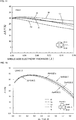
Fig. 4 shows the change in electromechanical coupling coefficient k2 of an SH plate wave SH0 in the case where the thickness of LiNbO3 is 0.05λ, 0.1λ, 0.15λ, 0.25λ, or 0.35λ and θ of the Euler angles (0°, e, 0°) of each LiNbO3 substrate is varied. As is clear fromFig. 4 , when the thickness of LiNbO3 ranges from 0.05λ to 0.25λ and θ of the Euler angles ranges from 92° to 138°, the electromechanical coupling coefficient k2 of the SH plate wave SH0 is large, 0.30 or more. It is preferred that θ ranges from 105° to 132°, because the electromechanical coupling coefficient k2 can be increased to 0.33 or more. Thus, in order to increase the electromechanical coupling coefficient k2 of the SH plate wave propagating in LiNbO3, θ of the Euler angles of LiNbO3 needs to range from 92° to 138° and preferably ranges from 105° to 132°. - On the other hand,
Fig. 5 is a graph showing the relationship between the thickness of LiNbO3 substrates with Euler angles (0°, 120°, 0°) and the electromechanical coupling coefficient k2. As is clear fromFig. 5 , when the Euler angles are (0°, 120°, 0°) and the thickness of LiNbO3 is 0.25λ or less, the electromechanical coupling coefficient k2 of an SH plate wave SH0 can be adjusted to 0.33 or more. The thickness of LiNbO3 is preferably 0.2λ or less, because the electromechanical coupling coefficient k2 can be adjusted to 0.40 or more. The thickness thereof is more preferably 0.17λ or less, because the electromechanical coupling coefficient k2 can be adjusted to 0.43 or more. - As is clear from
Figs. 2 to 5 , in the case of using an SH plate wave propagating in LiNbO3 substrates, when θ of the Euler angles of the LiNbO3 substrates ranges from 92° to 138° and the thickness of the LiNbO3 substrates is 0.25λ or less, the electromechanical coupling coefficient k2 of the SH plate wave can be significantly increased. Incidentally, when the thickness of the LiNbO3 substrate is excessively small, the elastic wave device, which includes theIDT electrodes 4, has a significantly reduced mechanical strength. In addition, it is difficult to assemble theelastic wave device 1 because of too small thickness. Thus, the thickness of the LiNbO3 substrate needs to be 0.05λ or more. - Next, in the
elastic wave device 1, the relationship between the thickness of theIDT electrodes 4 and bandwidth ratio has been investigated. Incidentally, the bandwidth ratio and the electromechanical coupling coefficient k2 are in a proportional relationship. - IDT electrodes made of various metals were formed using LiNbO3 substrates having Euler angles (0°, 120°, 0°) and a thickness of 0.1λ. In this structure, the IDT electrodes were varied in thickness and the fractional bandwidth Δf/f was determined. Incidentally, Δf is the difference between the antiresonant frequency fa and the resonant frequency f. That is, Δf equals fa minus f.
- As is clear from
Fig. 6 , even when the IDT electrodes are made of Al, Ni, Cu, Pt, or Au, the fractional bandwidth Δf/f tends to decrease with the increase in thickness of the IDT electrodes. -
Fig. 7 is a graph showing the relationship between the thickness of IDT electrodes and reflection coefficient in the above structure. It is clear fromFig. 7 that even when being made of any metal, the reflection coefficient increases with the increase in thickness of the IDT electrodes. - From results shown in
Figs. 6 and 7 , it is clear that when the thickness of the IDT electrodes is within a range shown in Table 5 below, the fractional bandwidth can be increased and the reflection coefficient can be increased to 0.1 or more. - Herein, for metals making up IDT electrodes, metals shown in Table 1 may be major components. A metal different from the metals shown in Table 1 may be deposited.
- Even when IDT electrodes are made of a metal other than the metals shown in Table 1, that is, a metal having a density between 2.699 x 10³ kg/m3, which is the density of Al, and 21.45 x 10³ kg/m3, which is the density of Pt, characteristics similar to characteristics shown in
Figs. 6 and 7 can be obtained. In particular, the IDT electrodes are preferably made of a metal having a density between 2.699 x 10³ kg/m3, which is the density of Al, and 8.93 x 10³ kg/m3, which is the density of Cu.[Table 5] Δf/f: 25% or more Δf/f: 27% or more Δf/f: 29% or more Thickness of IDT electrode Thickness of IDT electrode Thickness of IDT electrode Pt More than 0 to 0.083λ or less More than 0 to 0.05λ or less More than 0 to 0.02λ or less Au More than 0 to 0.055λ or less 0.035λ or less 0.015λ or less Cu More than 0 to 0.11λ or less 0.073λ or less 0.04λ or less Ni More than 0 to 0.16λ or less 0.105λ or less 0.055λ or less Al More than 0 to 0.135λ or less 0.105λ or less 0.065λ or less - The thickness of the IDT electrodes is preferably within a range specified in the leftmost column of Table 5, because the fractional bandwidth can be adjusted to 25% or more. The thickness of the IDT electrodes is more preferably within a range specified in the second column from the left, because the fractional bandwidth can be adjusted to 27% or more. The thickness of the IDT electrodes is further more preferably within a range specified in the rightmost column of Table 5, because the fractional bandwidth can be increased to 29% or more.
- Next, IDT electrodes made of various metals were provided on LiNbO3 substrates having Euler angles (0°, 116° to 118°, 0°) and a thickness of 0.1λ so as to have a thickness of 0.02λ to 0.04λ. Note that the duty ratio of the IDT electrodes was varied.
Fig. 8 shows the relationship between the duty ratio of the IDT electrodes and the fractional bandwidth.Fig. 9 shows the relationship between the duty ratio and reflection coefficient of the IDT electrodes. - As is clear from
Fig. 8 , in the case of using any metal, when the duty ratio is 0.85 or less, the fractional bandwidth increases as the duty ratio increases from 0.1. However, the fractional bandwidth tends to gradually decrease as the duty ratio exceeds 0.4. Likewise, the reflection coefficient increases as the duty ratio increases from 0.1. The reflection coefficient tends to significantly decrease as the duty ratio exceeds 0.7. When the Euler angles are (0°, 92° to 138°, 0°), the relationship between the duty ratio and the fractional bandwidth Δf/f is on the same trend. - From results shown in
Figs. 8 and 9 , it is clear that in the case where electrodes made of each metal are used, the fractional bandwidth Δf/f can be increased and a sufficient reflection coefficient can be obtained in such a way that the duty ratio of the IDT electrodes is adjusted within a range shown in Table 6 below. - Herein, for metals making up IDT electrodes, the metals shown in Table 1 may be major components. A metal different from the metals shown in Table 1 may be deposited.
- Even when IDT electrodes are made of a metal other than the metals shown in Table 1, that is, a metal having a density between 2.699 x 10³ kg/m3, which is the density of Al, and 21.45 × 10³ kg/m3, which is the density of Pt, characteristics similar to characteristics shown in
Figs. 8 and 9 can be obtained. In particular, the IDT electrodes are preferably made of a metal having a density between 2.699 × 10³ kg/m3, which is the density of Al, and 8.93 x 10³ kg/m3, which is the density of Cu.[Table 6] Δf/f: 26% or more Δf/f: 27% or more Δf/f: 30% or more Duty ratio Duty ratio Duty ratio Pt 0.105 to 0.62 0.11 to 0.58 0.22 to 0.43 Au 0.105 to 0.585 0.11 to 0.55 0.25 to 0.40 Cu 0.11 to 0.645 0.12 to 0.62 0.22 to 0.46 Ni 0.11 to 0.655 0.12 to 0.63 0.22 to 0.49 Al 0.115 to 0.63 0.13 to 0.60 0.25 to 0.47 - The duty ratio of the IDT electrodes is preferably within a range specified in the leftmost column of Table 6, because the fractional bandwidth Δf/f can be adjusted to 26% or more. The duty ratio of the IDT electrodes is more preferably within a range specified in the second column from the left of Table 6, because the fractional bandwidth can be adjusted to 27% or more. The duty ratio of the IDT electrodes is further more preferably within a range specified in the rightmost column of Table 6, because the fractional bandwidth can be significantly increased to 30% or more.
-
Fig. 10 is a front sectional view of an elastic wave device according to a second embodiment of the present invention. In theelastic wave device 21 of the second embodiment,IDT electrodes 4 are placed on the upper surface of a LiNbO3 substrate 3 andIDT electrodes 22 are placed on the lower surface thereof. That is, the electrodes are placed on both surfaces of the LiNbO3 substrate 3. Incidentally, the electrode structures of both surfaces are the same. Thus, a pair of reflectors, which are not shown, are placed on the lower surface. - In the present invention, the
IDT electrodes elastic wave device 21. -
Fig. 11 is a graph showing the relationship between the thickness of LiNbO3 and the acoustic velocity of an SH plate wave in the case whereIDT electrodes - As is clear from
Fig. 11 , in a structure in which the IDT electrodes are placed on both surfaces, the acoustic velocity of the SH plate wave does not significantly vary even though the thickness of LiNbO3 varies. - A solid line in
Fig. 12 represents the relationship between the thickness of LiNbO3 having a structure in which IDT electrodes which have a thickness of 0.02λ and which are made of Al are placed on both surfaces of each of LiNbO3 substrates with Euler angles (0°, 118°, 0°) and the fractional bandwidth. For comparison, a broken line represents the relationship between the fractional bandwidth and the thickness of LiNbO3 substrates having a structure in which IDT electrodes which have a thickness of 0.04λ and which are made of Al are placed on a single surface of each of the LiNbO3 substrates. - As is clear from
Fig. 12 , in the structure in which the IDT electrodes made of Al are placed on both surfaces, the fractional bandwidth can be significantly increased over a wide range when the sum of the thicknesses of the IDT electrodes is equal to the sum of the thicknesses of the comparative IDT electrodes. It is clear that when the thickness of the LiNbO3 substrate ranges from 0.02λ to 0.27λ, the fractional bandwidth Δf/f can be adjusted to 27% or more. The thickness of the LiNbO3 substrate more preferably ranges from 0.02λ to 0.15λ, because the fractional bandwidth Δf/f can be adjusted to 30% or more. - On the other hand,
Fig. 13 is a graph showing the relationship between the thickness of single-side IDT electrodes and the fractional bandwidth Δf/f in the case where the thickness of LiNbO3 is 0.15λ and IDT electrodes made of various different metals are placed on both surfaces of each substrate. As is clear fromFig. 13 , in a structure in which the IDT electrodes are placed on both surfaces, when the thickness of the single-side IDT electrodes ranges from more than 0 to 0.1λ, a large fractional bandwidth is obtained even though the electrodes are made of various metals. - In
Fig. 13 , the thickness of the LiNbO3 substrate is 0.15λ.Fig. 14 shows results obtained in the case where the thickness of LiNbO3 is 0.1λ. As is clear fromFig. 14 , when the thickness of single-side IDT electrodes ranges from more than 0 to 0.1λ, the fractional bandwidth can be increased even in the case where the thickness of the LiNbO3 substrate is 0.1λ and any metal is used. - As is clear from
Fig. 14 , when IDTs are made of various metals and the thickness of the single-side IDT electrodes is within a range shown in Table 7 below, the fractional bandwidth can be effectively increased.[Table 7] Metal making up electrode Δf/f: 27% or more Δf/f: 30% or more Thickness of single-side IDT electrodes Thickness of single-side IDT electrodes Pt More than 0 to 0.14λ or less - Au More than 0 to 0.067λ or less - Cu More than 0 to 0.145λ or less More than 0 to 0.045λ or less Ni 0.002λ to 0.20λ More than 0 to 0.102λ or less Al More than 0 to 0.125λ or less More than 0 to 0.057λ or less - As is clear from Table 7, when the thickness is within a range specified in the left column of Table 7, the fractional bandwidth can be adjusted to 27% or more. The thickness is more preferably within a range specified in the right column of Table 7, because the fractional bandwidth can be significantly increased to 30% or more. Thus, in the
elastic wave device 21, in which the IDT electrodes are placed on both surfaces, the thickness of the single-side IDT electrodes is preferably within a range specified in Table 7. - Next,
Fig. 15 shows the relationship between the duty ratio of IDT electrodes and the fractional bandwidth of theelastic wave device 21 in the case where the IDT electrodes are made of various metals and have a thickness of 0.02λ, 0.03λ, or 0.04λ. As is clear fromFig. 15 , the fractional bandwidth Δf/f increases with the increase of the duty ratio and the duty ratio tends to decrease again as the duty ratio exceeds a range from 0.2 to 0.25 even in the case of using any metal. It is clear fromFig. 15 that the fractional bandwidth can be increased in such a way that the duty ratio is adjusted within a range specified in Table 8 below depending on the type of a metal making up the IDT electrodes.[Table 8] Metal making up electrode Δf/f: 28% or more Δf/f: 30% or more Δf/f: 32% or more Duty ratio Duty ratio Duty ratio Pt 0.018 to 0.547 0.05 to 0.5 0.08 to 0.41 Au 0.018 to 0.523 0.05 to 0.47 0.10 to 0.38 Ni 0.018 to 0.597 0.05 to 0.55 0.10 to 0.46 Cu 0.018 to 0.567 0.05 to 0.52 0.10 to 0.43 Al 0.025 to 0.56 0.07 to 0.52 0.12 to 0.43 - As is clear from Table 8, when the duty ratio is within a range specified in the leftmost column of Table 8, the fractional bandwidth can be increased to 28% or more. The duty ratio is more preferably within a range specified in the second column from the left of Table 8, because the fractional bandwidth can be increased to 30% or more. The duty ratio is further more preferably within a range specified in the rightmost column of Table 8, because the fractional bandwidth can be increased to 32% or more.
- In first and second embodiments, the
support 2 used has the through-hole 2a. A support substrate with an upper surface having a recessed portion facing a region provided with IDT electrodes may be used instead of thesupport 2. - That is, the following structure can be used: an appropriate structure in which a portion of a LiNbO3 substrate that is provided with IDT electrodes can be mechanically freed.
- The electrode structure of an elastic wave device is not limited to the one port-type elastic wave resonator shown in
Fig. 1(b) . An appropriate electrode structure can be used depending on a resonator or filter making use of an elastic wave. -
- 1
- Elastic wave device
- 2
- Support
- 2a
- Through-hole
- 3
- LiNbO3 substrate
- 4
- IDT electrodes
- 5, 6
- Reflectors
- 21
- Elastic wave device
- 22
- IDT electrodes
Claims (7)
- An elastic wave device making use of an SH plate wave propagating in LiNbO3 substrates, comprising:a LiNbO3 substrate;IDT electrodes placed on at least one surface of the LiNbO3 substrate; anda support which is placed on the LiNbO3 substrate such that the support is located outside a region provided with the IDT electrodes and supports the LiNbO3 substrate,wherein θ of the Euler angles (0°, θ, 0°) of the LiNbO3 substrate ranges from 92° to 138° and the thickness of the LiNbO3 substrate ranges from 0.05λ to 0.25λ, where λ is the wavelength determined by the pitch between electrode fingers of the IDT electrodes.
- The elastic wave device according to Claim 1, wherein the IDT electrodes are made of a metal containing one of metals shown in Table 1 below as a major component and have a thickness within a range specified in Table 1 depending on the type of the metal:
[Table 1] Thickness of IDT electrode Pt More than 0 to 0.083λ or less Au More than 0 to 0.055λ or less Cu More than 0 to 0.11λ or less Ni More than 0 to 0.16λ or less Al More than 0 to 0.135λ or less - The elastic wave device according to Claim 1 or 2, wherein the IDT electrodes are made of a metal containing one of metals shown in Table 2 below as a major component and the duty ratio is within a range specified in Table 2 depending on the type of the metal:
[Table 2] Duty ratio Pt 0.105 to 0.62 Au 0.105 to 0.585 Cu 0.11 to 0.645 Ni 0.11 to 0.655 Al 0.115 to 0.63 - The elastic wave device according to Claim 1, wherein the IDT electrodes are placed on both surfaces of the LiNbO3 substrate, the IDT electrodes are made of a metal containing one of metals shown in Table 3 below as a major component, and the thickness of the IDT electrodes is within a range specified in Table 3 depending on the type of the metal:
[Table 3] Metal making up electrode Thickness of single-side IDT electrodes Pt More than 0 to 0.14λ or less Au More than 0 to 0.067λ or less Cu More than 0 to 0.145λ or less Ni 0.002λ to 0.20λ Al More than 0 to 0.125λ or less - The elastic wave device according to Claim 1 or 4, wherein the IDT electrodes are placed on both surfaces of the LiNbO3 substrate and the duty ratio of the IDT electrodes is within a range specified in Table 4 below depending on the type of a metal making up the IDT electrodes:
[Table 4] Metal making up electrode Duty ratio Pt 0.018 to 0.547 Au 0.018 to 0.523 Ni 0.018 to 0.597 Cu 0.018 to 0.567 Al 0.025 to 0.56 - The elastic wave device according to any one of Claims 1 to 5, wherein the support is a support substrate having a through-hole facing a region provided with the I DT electrodes.
- The elastic wave device according to any one of Claims 1 to 6, wherein the IDT electrodes are made of a metal containing a metal having a density between 2.699 × 10³ kg/m3 to 8.93 × 10³ kg/m3 as a major component.
Applications Claiming Priority (2)
| Application Number | Priority Date | Filing Date | Title |
|---|---|---|---|
| JP2011173120 | 2011-08-08 | ||
| PCT/JP2012/069865 WO2013021948A1 (en) | 2011-08-08 | 2012-08-03 | Elastic wave device |
Publications (3)
| Publication Number | Publication Date |
|---|---|
| EP2744107A1 true EP2744107A1 (en) | 2014-06-18 |
| EP2744107A4 EP2744107A4 (en) | 2015-03-25 |
| EP2744107B1 EP2744107B1 (en) | 2020-01-15 |
Family
ID=47668456
Family Applications (1)
| Application Number | Title | Priority Date | Filing Date |
|---|---|---|---|
| EP12822720.4A Active EP2744107B1 (en) | 2011-08-08 | 2012-08-03 | Elastic wave device |
Country Status (5)
| Country | Link |
|---|---|
| US (1) | US9564873B2 (en) |
| EP (1) | EP2744107B1 (en) |
| JP (1) | JP5747987B2 (en) |
| CN (1) | CN103718458B (en) |
| WO (1) | WO2013021948A1 (en) |
Cited By (1)
| Publication number | Priority date | Publication date | Assignee | Title |
|---|---|---|---|---|
| US10312883B2 (en) | 2014-03-14 | 2019-06-04 | Murata Manufacturing Co., Ltd. | Elastic wave device |
Families Citing this family (170)
| Publication number | Priority date | Publication date | Assignee | Title |
|---|---|---|---|---|
| JPWO2015137089A1 (en) * | 2014-03-14 | 2017-04-06 | 株式会社村田製作所 | Elastic wave device |
| WO2016047255A1 (en) * | 2014-09-26 | 2016-03-31 | 国立大学法人東北大学 | Elastic wave device |
| DE102014118000A1 (en) * | 2014-12-05 | 2016-06-09 | Epcos Ag | Arrangement with a strain gauge filter and steep right flank |
| CN106154186B (en) * | 2016-06-20 | 2020-01-17 | 瑞声声学科技(常州)有限公司 | Surface acoustic wave magnetic sensor and preparation method thereof |
| CN110249527B (en) * | 2017-02-14 | 2024-01-23 | 京瓷株式会社 | elastic wave element |
| CN110582938B (en) | 2017-04-26 | 2023-06-23 | 株式会社村田制作所 | elastic wave device |
| US11996827B2 (en) | 2018-06-15 | 2024-05-28 | Murata Manufacturing Co., Ltd. | Transversely-excited film bulk acoustic resonator with periodic etched holes |
| US10491192B1 (en) * | 2018-06-15 | 2019-11-26 | Resonant Inc. | Transversely-excited film bulk acoustic resonator |
| US10601392B2 (en) | 2018-06-15 | 2020-03-24 | Resonant Inc. | Solidly-mounted transversely-excited film bulk acoustic resonator |
| US11936358B2 (en) | 2020-11-11 | 2024-03-19 | Murata Manufacturing Co., Ltd. | Transversely-excited film bulk acoustic resonator with low thermal impedance |
| US11323090B2 (en) | 2018-06-15 | 2022-05-03 | Resonant Inc. | Transversely-excited film bulk acoustic resonator using Y-X-cut lithium niobate for high power applications |
| US10790802B2 (en) | 2018-06-15 | 2020-09-29 | Resonant Inc. | Transversely excited film bulk acoustic resonator using rotated Y-X cut lithium niobate |
| US10637438B2 (en) | 2018-06-15 | 2020-04-28 | Resonant Inc. | Transversely-excited film bulk acoustic resonators for high power applications |
| US11323089B2 (en) | 2018-06-15 | 2022-05-03 | Resonant Inc. | Filter using piezoelectric film bonded to high resistivity silicon substrate with trap-rich layer |
| US12040779B2 (en) | 2020-04-20 | 2024-07-16 | Murata Manufacturing Co., Ltd. | Small transversely-excited film bulk acoustic resonators with enhanced Q-factor |
| US11206009B2 (en) | 2019-08-28 | 2021-12-21 | Resonant Inc. | Transversely-excited film bulk acoustic resonator with interdigital transducer with varied mark and pitch |
| US12088281B2 (en) | 2021-02-03 | 2024-09-10 | Murata Manufacturing Co., Ltd. | Transversely-excited film bulk acoustic resonator with multi-mark interdigital transducer |
| US11323096B2 (en) | 2018-06-15 | 2022-05-03 | Resonant Inc. | Transversely-excited film bulk acoustic resonator with periodic etched holes |
| US11929731B2 (en) | 2018-02-18 | 2024-03-12 | Murata Manufacturing Co., Ltd. | Transversely-excited film bulk acoustic resonator with optimized electrode mark, and pitch |
| US10911023B2 (en) | 2018-06-15 | 2021-02-02 | Resonant Inc. | Transversely-excited film bulk acoustic resonator with etch-stop layer |
| US11146232B2 (en) | 2018-06-15 | 2021-10-12 | Resonant Inc. | Transversely-excited film bulk acoustic resonator with reduced spurious modes |
| US12237826B2 (en) | 2018-06-15 | 2025-02-25 | Murata Manufacturing Co., Ltd. | Transversely-excited film bulk acoustic resonator with optimized electrode thickness, mark, and pitch |
| US10756697B2 (en) | 2018-06-15 | 2020-08-25 | Resonant Inc. | Transversely-excited film bulk acoustic resonator |
| US11509279B2 (en) | 2020-07-18 | 2022-11-22 | Resonant Inc. | Acoustic resonators and filters with reduced temperature coefficient of frequency |
| US12224732B2 (en) | 2018-06-15 | 2025-02-11 | Murata Manufacturing Co., Ltd. | Solidly-mounted transversely-excited film bulk acoustic resonators and filters for 27 GHz communications bands |
| US10992284B2 (en) | 2018-06-15 | 2021-04-27 | Resonant Inc. | Filter using transversely-excited film bulk acoustic resonators with multiple frequency setting layers |
| US12009798B2 (en) | 2018-06-15 | 2024-06-11 | Murata Manufacturing Co., Ltd. | Transversely-excited film bulk acoustic resonators with electrodes having irregular hexagon cross-sectional shapes |
| US11996822B2 (en) | 2018-06-15 | 2024-05-28 | Murata Manufacturing Co., Ltd. | Wide bandwidth time division duplex transceiver |
| US10985728B2 (en) | 2018-06-15 | 2021-04-20 | Resonant Inc. | Transversely-excited film bulk acoustic resonator and filter with a uniform-thickness dielectric overlayer |
| US11967945B2 (en) | 2018-06-15 | 2024-04-23 | Murata Manufacturing Co., Ltd. | Transversly-excited film bulk acoustic resonators and filters |
| US10917072B2 (en) | 2019-06-24 | 2021-02-09 | Resonant Inc. | Split ladder acoustic wave filters |
| US12463619B2 (en) | 2018-06-15 | 2025-11-04 | Murata Manufacturing Co., Ltd. | Filter device |
| US12301212B2 (en) | 2018-06-15 | 2025-05-13 | Murata Manufacturing Co., Ltd. | XBAR resonators with non-rectangular diaphragms |
| US12040781B2 (en) | 2018-06-15 | 2024-07-16 | Murata Manufacturing Co., Ltd. | Transversely-excited film bulk acoustic resonator package |
| US11201601B2 (en) | 2018-06-15 | 2021-12-14 | Resonant Inc. | Transversely-excited film bulk acoustic resonator with multiple diaphragm thicknesses and fabrication method |
| US11171629B2 (en) | 2018-06-15 | 2021-11-09 | Resonant Inc. | Transversely-excited film bulk acoustic resonator using pre-formed cavities |
| US12244295B2 (en) | 2018-06-15 | 2025-03-04 | Murata Manufacturing Co., Ltd. | Transversely-excited film bulk acoustic resonators with two-layer electrodes having a narrower top layer |
| US11909381B2 (en) | 2018-06-15 | 2024-02-20 | Murata Manufacturing Co., Ltd. | Transversely-excited film bulk acoustic resonators with two-layer electrodes having a narrower top layer |
| US12155374B2 (en) | 2021-04-02 | 2024-11-26 | Murata Manufacturing Co., Ltd. | Tiled transversely-excited film bulk acoustic resonator high power filters |
| US10797675B2 (en) | 2018-06-15 | 2020-10-06 | Resonant Inc. | Transversely excited film bulk acoustic resonator using rotated z-cut lithium niobate |
| US11146238B2 (en) | 2018-06-15 | 2021-10-12 | Resonant Inc. | Film bulk acoustic resonator fabrication method |
| US11264966B2 (en) | 2018-06-15 | 2022-03-01 | Resonant Inc. | Solidly-mounted transversely-excited film bulk acoustic resonator with diamond layers in Bragg reflector stack |
| US12218650B2 (en) | 2018-06-15 | 2025-02-04 | Murata Manufacturing Co., Ltd. | Transversely-excited film bulk acoustic resonator |
| US11901878B2 (en) | 2018-06-15 | 2024-02-13 | Murata Manufacturing Co., Ltd. | Transversely-excited film bulk acoustic resonators with two-layer electrodes with a wider top layer |
| US12155371B2 (en) | 2021-03-29 | 2024-11-26 | Murata Manufacturing Co., Ltd. | Layout of xbars with multiple sub-resonators in series |
| US12212306B2 (en) | 2018-06-15 | 2025-01-28 | Murata Manufacturing Co., Ltd. | Transversely-excited film bulk acoustic resonator with multiple diaphragm thicknesses and fabrication method |
| US11949402B2 (en) | 2020-08-31 | 2024-04-02 | Murata Manufacturing Co., Ltd. | Resonators with different membrane thicknesses on the same die |
| US11323095B2 (en) | 2018-06-15 | 2022-05-03 | Resonant Inc. | Rotation in XY plane to suppress spurious modes in XBAR devices |
| US11374549B2 (en) | 2018-06-15 | 2022-06-28 | Resonant Inc. | Filter using transversely-excited film bulk acoustic resonators with divided frequency-setting dielectric layers |
| US10819309B1 (en) | 2019-04-05 | 2020-10-27 | Resonant Inc. | Transversely-excited film bulk acoustic resonator package and method |
| US12184261B2 (en) | 2018-06-15 | 2024-12-31 | Murata Manufacturing Co., Ltd. | Transversely-excited film bulk acoustic resonator with a cavity having round end zones |
| US11329628B2 (en) | 2020-06-17 | 2022-05-10 | Resonant Inc. | Filter using lithium niobate and lithium tantalate transversely-excited film bulk acoustic resonators |
| US11323091B2 (en) | 2018-06-15 | 2022-05-03 | Resonant Inc. | Transversely-excited film bulk acoustic resonator with diaphragm support pedestals |
| US10826462B2 (en) * | 2018-06-15 | 2020-11-03 | Resonant Inc. | Transversely-excited film bulk acoustic resonators with molybdenum conductors |
| US10992283B2 (en) | 2018-06-15 | 2021-04-27 | Resonant Inc. | High power transversely-excited film bulk acoustic resonators on rotated Z-cut lithium niobate |
| US12095446B2 (en) | 2018-06-15 | 2024-09-17 | Murata Manufacturing Co., Ltd. | Transversely-excited film bulk acoustic resonator with optimized electrode thickness, mark, and pitch |
| US11349450B2 (en) | 2018-06-15 | 2022-05-31 | Resonant Inc. | Symmetric transversely-excited film bulk acoustic resonators with reduced spurious modes |
| US12283944B2 (en) | 2018-06-15 | 2025-04-22 | Murata Manufacturing Co., Ltd. | Transversely-excited film bulk acoustic resonator with recessed rotated-Y-X cut lithium niobate |
| US10998882B2 (en) | 2018-06-15 | 2021-05-04 | Resonant Inc. | XBAR resonators with non-rectangular diaphragms |
| US11876498B2 (en) | 2018-06-15 | 2024-01-16 | Murata Manufacturing Co., Ltd. | Transversely-excited film bulk acoustic resonator with multiple diaphragm thicknesses and fabrication method |
| US12375056B2 (en) | 2018-06-15 | 2025-07-29 | Murata Manufacturing Co., Ltd. | Transversely-excited film bulk acoustic resonators |
| US11349452B2 (en) | 2018-06-15 | 2022-05-31 | Resonant Inc. | Transversely-excited film bulk acoustic filters with symmetric layout |
| US12170516B2 (en) | 2018-06-15 | 2024-12-17 | Murata Manufacturing Co., Ltd. | Filters using transversly-excited film bulk acoustic resonators with frequency-setting dielectric layers |
| US11888463B2 (en) | 2018-06-15 | 2024-01-30 | Murata Manufacturing Co., Ltd. | Multi-port filter using transversely-excited film bulk acoustic resonators |
| US10868513B2 (en) | 2018-06-15 | 2020-12-15 | Resonant Inc. | Transversely-excited film bulk acoustic filters with symmetric layout |
| US12119805B2 (en) | 2018-06-15 | 2024-10-15 | Murata Manufacturing Co., Ltd. | Substrate processing and membrane release of transversely-excited film bulk acoustic resonator using a sacrificial tub |
| US12191838B2 (en) | 2018-06-15 | 2025-01-07 | Murata Manufacturing Co., Ltd. | Solidly-mounted transversely-excited film bulk acoustic device and method |
| US11996825B2 (en) | 2020-06-17 | 2024-05-28 | Murata Manufacturing Co., Ltd. | Filter using lithium niobate and rotated lithium tantalate transversely-excited film bulk acoustic resonators |
| US12095441B2 (en) | 2018-06-15 | 2024-09-17 | Murata Manufacturing Co., Ltd. | Transversely excited film bulk acoustic resonator with recessed interdigital transducer fingers |
| US11916539B2 (en) | 2020-02-28 | 2024-02-27 | Murata Manufacturing Co., Ltd. | Split-ladder band N77 filter using transversely-excited film bulk acoustic resonators |
| US12119808B2 (en) | 2018-06-15 | 2024-10-15 | Murata Manufacturing Co., Ltd. | Transversely-excited film bulk acoustic resonator package |
| US12149227B2 (en) | 2018-06-15 | 2024-11-19 | Murata Manufacturing Co., Ltd. | Transversely-excited film bulk acoustic resonator package |
| US12081187B2 (en) | 2018-06-15 | 2024-09-03 | Murata Manufacturing Co., Ltd. | Transversely-excited film bulk acoustic resonator |
| US11728785B2 (en) | 2018-06-15 | 2023-08-15 | Murata Manufacturing Co., Ltd. | Transversely-excited film bulk acoustic resonator using pre-formed cavities |
| US12132464B2 (en) | 2018-06-15 | 2024-10-29 | Murata Manufacturing Co., Ltd. | Filter using transversely-excited film bulk acoustic resonators with divided frequency-setting dielectric layers |
| US12113512B2 (en) | 2021-03-29 | 2024-10-08 | Murata Manufacturing Co., Ltd. | Layout of XBARs with multiple sub-resonators in parallel |
| US12191837B2 (en) | 2018-06-15 | 2025-01-07 | Murata Manufacturing Co., Ltd. | Solidly-mounted transversely-excited film bulk acoustic device |
| US12237827B2 (en) | 2018-06-15 | 2025-02-25 | Murata Manufacturing Co., Ltd. | Solidly-mounted transversely-excited film bulk acoustic filters with multiple piezoelectric plate thicknesses |
| US11228296B2 (en) | 2018-06-15 | 2022-01-18 | Resonant Inc. | Transversely-excited film bulk acoustic resonator with a cavity having a curved perimeter |
| US10998877B2 (en) | 2018-06-15 | 2021-05-04 | Resonant Inc. | Film bulk acoustic resonator fabrication method with frequency trimming based on electric measurements prior to cavity etch |
| US12021496B2 (en) | 2020-08-31 | 2024-06-25 | Murata Manufacturing Co., Ltd. | Resonators with different membrane thicknesses on the same die |
| US11870423B2 (en) | 2018-06-15 | 2024-01-09 | Murata Manufacturing Co., Ltd. | Wide bandwidth temperature-compensated transversely-excited film bulk acoustic resonator |
| DE112019005403T5 (en) | 2018-10-31 | 2021-07-15 | Resonant Inc. | FIXED MOUNTED TRANSVERSAL EXCITED ACOUSTIC FILM VOLUME RESONATOR |
| WO2020100949A1 (en) * | 2018-11-14 | 2020-05-22 | 京セラ株式会社 | Elastic wave device, duplexer, and communication device |
| US11901873B2 (en) | 2019-03-14 | 2024-02-13 | Murata Manufacturing Co., Ltd. | Transversely-excited film bulk acoustic resonator with partial BRAGG reflectors |
| CN113615083B (en) | 2019-03-14 | 2024-10-15 | 株式会社村田制作所 | Laterally excited film bulk acoustic resonator with half-λ dielectric layer |
| US10911021B2 (en) | 2019-06-27 | 2021-02-02 | Resonant Inc. | Transversely-excited film bulk acoustic resonator with lateral etch stop |
| US12034423B2 (en) | 2019-06-27 | 2024-07-09 | Murata Manufacturing Co., Ltd | XBAR frontside etch process using polysilicon sacrificial layer |
| US10862454B1 (en) | 2019-07-18 | 2020-12-08 | Resonant Inc. | Film bulk acoustic resonators in thin LN-LT layers |
| US11329625B2 (en) | 2019-07-18 | 2022-05-10 | Resonant Inc. | Film bulk acoustic sensors using thin LN-LT layer |
| CN114586282A (en) * | 2019-10-24 | 2022-06-03 | 京瓷株式会社 | Elastic wave device |
| CN113328721A (en) * | 2020-02-28 | 2021-08-31 | 谐振公司 | Transverse-excitation film bulk acoustic resonator with multi-pitch interdigital transducer |
| US12506462B2 (en) | 2020-02-28 | 2025-12-23 | Murata Manufacturing Co., Ltd. | Transversely-excited film bulk acoustic resonator with multi-pitch interdigital transducer |
| US12255625B2 (en) | 2020-02-28 | 2025-03-18 | Murata Manufacturing Co., Ltd. | Filter using transversely-excited film bulk acoustic resonators with inductively coupled sub-resonators |
| US12341490B2 (en) | 2020-04-20 | 2025-06-24 | Murata Manufacturing Co., Ltd. | Low loss transversely-excited film bulk acoustic resonators and filters |
| US12278617B2 (en) | 2020-04-20 | 2025-04-15 | Murata Manufacturing Co., Ltd. | High Q solidly-mounted transversely-excited film bulk acoustic resonators |
| US12341493B2 (en) | 2020-04-20 | 2025-06-24 | Murata Manufacturing Co., Ltd. | Low loss transversely-excited film bulk acoustic resonators and filters |
| US11811391B2 (en) | 2020-05-04 | 2023-11-07 | Murata Manufacturing Co., Ltd. | Transversely-excited film bulk acoustic resonator with etched conductor patterns |
| US11469733B2 (en) | 2020-05-06 | 2022-10-11 | Resonant Inc. | Transversely-excited film bulk acoustic resonators with interdigital transducer configured to reduce diaphragm stress |
| US12074584B2 (en) | 2020-05-28 | 2024-08-27 | Murata Manufacturing Co., Ltd. | Transversely-excited film bulk acoustic resonators with two-layer electrodes |
| US12267062B2 (en) * | 2020-06-17 | 2025-04-01 | Murata Manufacturing Co., Ltd. | Transversely-excited film bulk acoustic resonators with three-layer electrodes |
| US10992282B1 (en) | 2020-06-18 | 2021-04-27 | Resonant Inc. | Transversely-excited film bulk acoustic resonators with electrodes having a second layer of variable width |
| US11742828B2 (en) | 2020-06-30 | 2023-08-29 | Murata Manufacturing Co., Ltd. | Transversely-excited film bulk acoustic resonator with symmetric diaphragm |
| US11482981B2 (en) | 2020-07-09 | 2022-10-25 | Resonanat Inc. | Transversely-excited film bulk acoustic resonators with piezoelectric diaphragm supported by piezoelectric substrate |
| US11264969B1 (en) | 2020-08-06 | 2022-03-01 | Resonant Inc. | Transversely-excited film bulk acoustic resonator comprising small cells |
| US11271539B1 (en) | 2020-08-19 | 2022-03-08 | Resonant Inc. | Transversely-excited film bulk acoustic resonator with tether-supported diaphragm |
| US11671070B2 (en) | 2020-08-19 | 2023-06-06 | Murata Manufacturing Co., Ltd. | Transversely-excited film bulk acoustic resonators using multiple dielectric layer thicknesses to suppress spurious modes |
| US11894835B2 (en) | 2020-09-21 | 2024-02-06 | Murata Manufacturing Co., Ltd. | Sandwiched XBAR for third harmonic operation |
| US11405019B2 (en) | 2020-10-05 | 2022-08-02 | Resonant Inc. | Transversely-excited film bulk acoustic resonator matrix filters |
| US11476834B2 (en) | 2020-10-05 | 2022-10-18 | Resonant Inc. | Transversely-excited film bulk acoustic resonator matrix filters with switches in parallel with sub-filter shunt capacitors |
| US11405017B2 (en) | 2020-10-05 | 2022-08-02 | Resonant Inc. | Acoustic matrix filters and radios using acoustic matrix filters |
| US11929733B2 (en) | 2020-10-05 | 2024-03-12 | Murata Manufacturing Co., Ltd. | Transversely-excited film bulk acoustic resonator matrix filters with input and output impedances matched to radio frequency front end elements |
| US11658639B2 (en) | 2020-10-05 | 2023-05-23 | Murata Manufacturing Co., Ltd. | Transversely-excited film bulk acoustic resonator matrix filters with noncontiguous passband |
| US11728784B2 (en) | 2020-10-05 | 2023-08-15 | Murata Manufacturing Co., Ltd. | Transversely-excited film bulk acoustic resonator matrix filters with split die sub-filters |
| US11463066B2 (en) | 2020-10-14 | 2022-10-04 | Resonant Inc. | Transversely-excited film bulk acoustic resonators with piezoelectric diaphragm supported by piezoelectric substrate |
| US12119806B2 (en) * | 2020-10-30 | 2024-10-15 | Murata Manufacturing Co., Ltd. | Transversely-excited film bulk acoustic resonator with spiral interdigitated transducer fingers |
| CN116458061A (en) * | 2020-11-11 | 2023-07-18 | 株式会社村田制作所 | Filter device |
| CN116491068A (en) | 2020-11-11 | 2023-07-25 | 株式会社村田制作所 | elastic wave device |
| CN116530011A (en) * | 2020-11-11 | 2023-08-01 | 株式会社村田制作所 | Elastic wave device |
| US12255617B2 (en) | 2020-11-11 | 2025-03-18 | Murata Manufacturing Co., Ltd. | Solidly-mounted transversely-excited film bulk acoustic resonators with low thermal impedance |
| US12003226B2 (en) | 2020-11-11 | 2024-06-04 | Murata Manufacturing Co., Ltd | Transversely-excited film bulk acoustic resonator with low thermal impedance |
| US12431856B2 (en) | 2020-11-12 | 2025-09-30 | Murata Manufacturing Co., Ltd. | Transversely-excited film bulk acoustic resonator with reduced loss in the aperture direction |
| US11496113B2 (en) | 2020-11-13 | 2022-11-08 | Resonant Inc. | XBAR devices with excess piezoelectric material removed |
| US12362725B2 (en) | 2020-11-13 | 2025-07-15 | Murata Manufacturing Co., Ltd. | Transversely-excited film bulk acoustic filters with excess piezoelectric material removed |
| US12255626B2 (en) | 2020-11-13 | 2025-03-18 | Murata Manufacturing Co., Ltd. | Solidly-mounted transversely-excited film bulk acoustic filters with excess piezoelectric material removed |
| US12028039B2 (en) | 2020-11-13 | 2024-07-02 | Murata Manufacturing Co., Ltd. | Forming XBAR devices with excess piezoelectric material removed |
| US11405020B2 (en) | 2020-11-26 | 2022-08-02 | Resonant Inc. | Transversely-excited film bulk acoustic resonators with structures to reduce acoustic energy leakage |
| WO2022124391A1 (en) * | 2020-12-11 | 2022-06-16 | 株式会社村田製作所 | Elastic wave device |
| CN116636140A (en) | 2020-12-18 | 2023-08-22 | 株式会社村田制作所 | Elastic wave device |
| WO2022138328A1 (en) | 2020-12-23 | 2022-06-30 | 株式会社村田製作所 | Surface acoustic wave device |
| CN116671009A (en) | 2020-12-23 | 2023-08-29 | 株式会社村田制作所 | elastic wave device |
| US11239816B1 (en) | 2021-01-15 | 2022-02-01 | Resonant Inc. | Decoupled transversely-excited film bulk acoustic resonators |
| US12126318B2 (en) | 2021-01-15 | 2024-10-22 | Murata Manufacturing Co., Ltd. | Filters using decoupled transversely-excited film bulk acoustic resonators |
| US12166468B2 (en) | 2021-01-15 | 2024-12-10 | Murata Manufacturing Co., Ltd. | Decoupled transversely-excited film bulk acoustic resonators for high power filters |
| US12463615B2 (en) | 2021-01-21 | 2025-11-04 | Murata Manufacturing Co., Ltd | Transversely-excited film bulk acoustic resonators with improved coupling and reduced energy leakage |
| US12308826B2 (en) | 2021-02-03 | 2025-05-20 | Murata Manufacturing Co., Ltd. | Bandpass filters using transversely-excited film bulk acoustic resonators |
| US12113510B2 (en) | 2021-02-03 | 2024-10-08 | Murata Manufacturing Co., Ltd. | Transversely-excited film bulk acoustic resonators with multiple piezoelectric membrane thicknesses on the same chip |
| US12308825B2 (en) | 2021-02-12 | 2025-05-20 | Murata Manufacturing Co., Ltd | Transversely-excited film bulk acoustic resonators with narrow gaps between busbars and ends of interdigital transducer fingers |
| WO2022190743A1 (en) | 2021-03-10 | 2022-09-15 | 株式会社村田製作所 | Elastic wave device |
| US12289099B2 (en) | 2021-03-24 | 2025-04-29 | Murata Manufacturing Co., Ltd. | Acoustic filters with shared acoustic tracks for series and shunt resonators |
| US12126328B2 (en) | 2021-03-24 | 2024-10-22 | Murata Manufacturing Co., Ltd. | Acoustic filters with shared acoustic tracks |
| US12355426B2 (en) | 2021-03-24 | 2025-07-08 | Murata Manufacturing Co., Ltd. | Acoustic filters with shared acoustic tracks |
| US12348216B2 (en) | 2021-03-24 | 2025-07-01 | Murata Manufacturing Co., Ltd. | Acoustic filters with shared acoustic tracks and cascaded series resonators |
| WO2022202916A1 (en) | 2021-03-26 | 2022-09-29 | 株式会社村田製作所 | Elastic wave device |
| CN116868508A (en) | 2021-03-26 | 2023-10-10 | 株式会社村田制作所 | elastic wave device |
| US12341492B2 (en) | 2021-03-29 | 2025-06-24 | Murata Manufacturing Co., Ltd. | Transversely-excited film bulk acoustic resonators with busbar side edges that form angles with a perimeter of the cavity |
| CN120454674A (en) | 2021-03-30 | 2025-08-08 | 株式会社村田制作所 | Filter for 6 GHz Wi-Fi using laterally excited film bulk acoustic resonators |
| US12224735B2 (en) | 2021-03-30 | 2025-02-11 | Murata Manufacturing Co., Ltd. | Diplexer using decoupled transversely-excited film bulk acoustic resonators |
| US12249971B2 (en) | 2021-04-02 | 2025-03-11 | Murata Manufacturing Co., Ltd. | Transversely-excited film bulk acoustic resonators with solidly mounted resonator (SMR) pedestals |
| US12237823B2 (en) | 2021-04-02 | 2025-02-25 | Murata Manufacturing Co., Ltd. | Transversely-excited film bulk acoustic resonators with solidly mounted resonator (SMR) pedestals |
| US12255633B2 (en) | 2021-04-16 | 2025-03-18 | Murata Manufacturing Co., Ltd. | Filter using transversely-excited film bulk acoustic resonators |
| US12126316B2 (en) | 2021-04-16 | 2024-10-22 | Murata Manufacturing Co., Ltd | Transversely-excited film bulk acoustic resonator |
| US12160220B2 (en) | 2021-04-30 | 2024-12-03 | Murata Manufacturing Co., Ltd. | Transversely-excited film bulk acoustic resonator with oxide strip acoustic confinement structures |
| US12255607B2 (en) | 2021-04-30 | 2025-03-18 | Murata Manufacturing Co., Ltd. | Transversely-excited film bulk acoustic resonator with buried oxide strip acoustic confinement structures |
| US12075700B2 (en) | 2021-05-07 | 2024-08-27 | Murata Manufacturing Co., Ltd. | Transversely-excited film bulk acoustic resonator fabrication using polysilicon pillars |
| US12057823B2 (en) | 2021-05-07 | 2024-08-06 | Murata Manufacturing Co., Ltd. | Transversely-excited film bulk acoustic resonator with concentric interdigitated transducer fingers |
| US12170513B2 (en) | 2021-06-30 | 2024-12-17 | Murata Manufacturing Co., Ltd. | Transversely-excited film bulk acoustic resonator with reduced substrate to contact bump thermal resistance |
| US12603639B2 (en) | 2021-08-02 | 2026-04-14 | Murata Manufacturing Co., Ltd. | Metal cavity for transversely-excited film bulk acoustic resonator (XBAR) |
| US12456962B2 (en) | 2021-09-24 | 2025-10-28 | Murata Manufacturing Co., Ltd. | Transversely-excited film bulk acoustic resonators wafer-level packaging using a dielectric cover |
| US12451864B2 (en) | 2021-09-29 | 2025-10-21 | Murata Manufacturing Co., Ltd. | Transversely-excited film bulk acoustic resonators with curved shaped ends of fingers or opposing busbars |
| US12225387B2 (en) | 2021-09-29 | 2025-02-11 | Murata Manufacturing Co., Ltd. | Communications device with concurrent operation in 5GHZ and 6GHZ U-NII frequency ranges |
| US12407326B2 (en) | 2021-11-04 | 2025-09-02 | Murata Manufacturing Co., Ltd. | Stacked die transversely-excited film bulk acoustic resonator (XBAR) filters |
| CN118216087A (en) | 2021-12-02 | 2024-06-18 | 株式会社村田制作所 | Filter device |
| US12424999B2 (en) | 2021-12-28 | 2025-09-23 | Murata Manufacturing Co., Ltd. | Transversely-excited film bulk acoustic resonators with gap dielectric stripes in busbar-electrode gaps |
| US12494768B2 (en) | 2021-12-28 | 2025-12-09 | Murata Manufacturing Co., Ltd. | Transversely-excited film bulk acoustic resonators with gap dielectric stripes in busbar-electrode gaps |
| US12413196B2 (en) | 2022-02-16 | 2025-09-09 | Murata Manufacturing Co., Ltd. | Tuning acoustic resonators with back-side coating |
| US12549151B2 (en) | 2022-04-12 | 2026-02-10 | Murata Manufacturing Co., Ltd. | Transversely-excited film bulk acoustic resonator with thick dielectric layer for improved coupling |
| US12489417B2 (en) | 2022-04-12 | 2025-12-02 | Murata Manufacturing Co., Ltd. | Ladder filter with transversely-excited film bulk acoustic resonators having different pitches |
| WO2024034528A1 (en) * | 2022-08-12 | 2024-02-15 | 京セラ株式会社 | Elastic wave device, composite filter, and communication device |
| US12489415B2 (en) | 2022-10-19 | 2025-12-02 | Murata Manufacturing Co., Ltd. | Acoustic resonator lid for thermal transport |
Family Cites Families (12)
| Publication number | Priority date | Publication date | Assignee | Title |
|---|---|---|---|---|
| US5532538A (en) * | 1994-10-28 | 1996-07-02 | Jin; Yu | Sensing and signal processing devices using quasi-SH (shear horizontal) acoustic waves |
| JP2002152007A (en) * | 2000-11-15 | 2002-05-24 | Hitachi Ltd | Lamb wave type elastic wave resonator |
| JP2002368576A (en) | 2001-06-05 | 2002-12-20 | Fujitsu Media Device Kk | Surface acoustic wave element |
| DE112004001841B4 (en) * | 2003-10-03 | 2009-03-12 | Murata Mfg. Co., Ltd., Nagaokakyo-shi | Surface acoustic wave device |
| KR100904368B1 (en) * | 2005-10-19 | 2009-06-23 | 가부시키가이샤 무라타 세이사쿠쇼 | Lamb wave device |
| JP4315174B2 (en) * | 2006-02-16 | 2009-08-19 | セイコーエプソン株式会社 | Manufacturing method of lamb wave type high frequency device |
| EP2109218A4 (en) * | 2007-05-25 | 2012-11-28 | Panasonic Corp | ELASTIC WAVE ELEMENT |
| CN102089970A (en) * | 2008-07-11 | 2011-06-08 | 松下电器产业株式会社 | Plate wave element and electronic equipment using the plate wave element |
| JP4636292B2 (en) * | 2008-08-27 | 2011-02-23 | 株式会社村田製作所 | Electronic component and method for manufacturing electronic component |
| JP5433367B2 (en) * | 2008-11-19 | 2014-03-05 | 日本碍子株式会社 | Lamb wave device |
| US8689426B2 (en) * | 2008-12-17 | 2014-04-08 | Sand 9, Inc. | Method of manufacturing a resonating structure |
| DE112010000861B4 (en) * | 2009-01-15 | 2016-12-15 | Murata Manufacturing Co., Ltd. | Piezoelectric device and method of manufacturing a piezoelectric device |
-
2012
- 2012-08-03 CN CN201280038499.4A patent/CN103718458B/en active Active
- 2012-08-03 JP JP2013528012A patent/JP5747987B2/en active Active
- 2012-08-03 WO PCT/JP2012/069865 patent/WO2013021948A1/en not_active Ceased
- 2012-08-03 EP EP12822720.4A patent/EP2744107B1/en active Active
-
2014
- 2014-02-03 US US14/170,883 patent/US9564873B2/en active Active
Cited By (1)
| Publication number | Priority date | Publication date | Assignee | Title |
|---|---|---|---|---|
| US10312883B2 (en) | 2014-03-14 | 2019-06-04 | Murata Manufacturing Co., Ltd. | Elastic wave device |
Also Published As
| Publication number | Publication date |
|---|---|
| EP2744107A4 (en) | 2015-03-25 |
| WO2013021948A1 (en) | 2013-02-14 |
| CN103718458A (en) | 2014-04-09 |
| JPWO2013021948A1 (en) | 2015-03-05 |
| US9564873B2 (en) | 2017-02-07 |
| CN103718458B (en) | 2017-01-25 |
| JP5747987B2 (en) | 2015-07-15 |
| EP2744107B1 (en) | 2020-01-15 |
| US20140145556A1 (en) | 2014-05-29 |
Similar Documents
| Publication | Publication Date | Title |
|---|---|---|
| EP2744107A1 (en) | Elastic wave device | |
| CN113678372B (en) | High-order mode elastic surface wave devices | |
| US7569972B2 (en) | Surface acoustic wave device | |
| JP7433873B2 (en) | Acoustic wave resonators, filters, and multiplexers | |
| KR20190077224A (en) | Elastic wave device | |
| KR102722448B1 (en) | Elastic wave device | |
| US8304959B2 (en) | Surface acoustic wave device | |
| WO2017043427A1 (en) | Elastic wave device, high-frequency front-end circuit and communication device | |
| JPWO2011102128A1 (en) | Antenna duplexer | |
| JP7207526B2 (en) | Acoustic wave device | |
| JP6658957B2 (en) | Elastic wave device, high-frequency front-end circuit, and communication device | |
| JP5137828B2 (en) | Surface acoustic wave device | |
| US7705515B2 (en) | Surface acoustic wave device | |
| WO2018163805A1 (en) | Elastic wave device, high-frequency front end circuit, and communications device | |
| JP2023060058A (en) | Acoustic wave resonator, filter and multiplexer | |
| JP6624337B2 (en) | Elastic wave device, multiplexer, high-frequency front-end circuit, and communication device | |
| JPWO2020209190A1 (en) | Elastic wave device and multiplexer | |
| WO2014054580A1 (en) | Elastic surface wave device | |
| JP7587766B2 (en) | Resonator | |
| WO2022168798A1 (en) | Elastic wave device | |
| JP2020129787A (en) | Acoustic wave resonator, filter and multiplexer | |
| JP7575023B2 (en) | Surface Acoustic Wave Devices | |
| JP2007251710A (en) | Surface acoustic wave device | |
| JP4507819B2 (en) | Surface acoustic wave device |
Legal Events
| Date | Code | Title | Description |
|---|---|---|---|
| PUAI | Public reference made under article 153(3) epc to a published international application that has entered the european phase |
Free format text: ORIGINAL CODE: 0009012 |
|
| 17P | Request for examination filed |
Effective date: 20140203 |
|
| AK | Designated contracting states |
Kind code of ref document: A1 Designated state(s): AL AT BE BG CH CY CZ DE DK EE ES FI FR GB GR HR HU IE IS IT LI LT LU LV MC MK MT NL NO PL PT RO RS SE SI SK SM TR |
|
| DAX | Request for extension of the european patent (deleted) | ||
| A4 | Supplementary search report drawn up and despatched |
Effective date: 20150219 |
|
| RIC1 | Information provided on ipc code assigned before grant |
Ipc: H03H 9/02 20060101AFI20150213BHEP |
|
| REG | Reference to a national code |
Ref country code: DE Ref legal event code: R079 Ref document number: 602012067308 Country of ref document: DE Free format text: PREVIOUS MAIN CLASS: H03H0009250000 Ipc: H03H0009020000 |
|
| GRAP | Despatch of communication of intention to grant a patent |
Free format text: ORIGINAL CODE: EPIDOSNIGR1 |
|
| STAA | Information on the status of an ep patent application or granted ep patent |
Free format text: STATUS: GRANT OF PATENT IS INTENDED |
|
| RIC1 | Information provided on ipc code assigned before grant |
Ipc: H03H 9/02 20060101AFI20190710BHEP |
|
| INTG | Intention to grant announced |
Effective date: 20190809 |
|
| GRAS | Grant fee paid |
Free format text: ORIGINAL CODE: EPIDOSNIGR3 |
|
| GRAA | (expected) grant |
Free format text: ORIGINAL CODE: 0009210 |
|
| STAA | Information on the status of an ep patent application or granted ep patent |
Free format text: STATUS: THE PATENT HAS BEEN GRANTED |
|
| AK | Designated contracting states |
Kind code of ref document: B1 Designated state(s): AL AT BE BG CH CY CZ DE DK EE ES FI FR GB GR HR HU IE IS IT LI LT LU LV MC MK MT NL NO PL PT RO RS SE SI SK SM TR |
|
| REG | Reference to a national code |
Ref country code: CH Ref legal event code: EP Ref country code: GB Ref legal event code: FG4D |
|
| REG | Reference to a national code |
Ref country code: IE Ref legal event code: FG4D |
|
| REG | Reference to a national code |
Ref country code: DE Ref legal event code: R096 Ref document number: 602012067308 Country of ref document: DE |
|
| REG | Reference to a national code |
Ref country code: AT Ref legal event code: REF Ref document number: 1226062 Country of ref document: AT Kind code of ref document: T Effective date: 20200215 |
|
| REG | Reference to a national code |
Ref country code: NL Ref legal event code: MP Effective date: 20200115 |
|
| REG | Reference to a national code |
Ref country code: LT Ref legal event code: MG4D |
|
| PG25 | Lapsed in a contracting state [announced via postgrant information from national office to epo] |
Ref country code: RS Free format text: LAPSE BECAUSE OF FAILURE TO SUBMIT A TRANSLATION OF THE DESCRIPTION OR TO PAY THE FEE WITHIN THE PRESCRIBED TIME-LIMIT Effective date: 20200115 Ref country code: PT Free format text: LAPSE BECAUSE OF FAILURE TO SUBMIT A TRANSLATION OF THE DESCRIPTION OR TO PAY THE FEE WITHIN THE PRESCRIBED TIME-LIMIT Effective date: 20200607 Ref country code: NL Free format text: LAPSE BECAUSE OF FAILURE TO SUBMIT A TRANSLATION OF THE DESCRIPTION OR TO PAY THE FEE WITHIN THE PRESCRIBED TIME-LIMIT Effective date: 20200115 Ref country code: NO Free format text: LAPSE BECAUSE OF FAILURE TO SUBMIT A TRANSLATION OF THE DESCRIPTION OR TO PAY THE FEE WITHIN THE PRESCRIBED TIME-LIMIT Effective date: 20200415 Ref country code: FI Free format text: LAPSE BECAUSE OF FAILURE TO SUBMIT A TRANSLATION OF THE DESCRIPTION OR TO PAY THE FEE WITHIN THE PRESCRIBED TIME-LIMIT Effective date: 20200115 |
|
| PG25 | Lapsed in a contracting state [announced via postgrant information from national office to epo] |
Ref country code: IS Free format text: LAPSE BECAUSE OF FAILURE TO SUBMIT A TRANSLATION OF THE DESCRIPTION OR TO PAY THE FEE WITHIN THE PRESCRIBED TIME-LIMIT Effective date: 20200515 Ref country code: GR Free format text: LAPSE BECAUSE OF FAILURE TO SUBMIT A TRANSLATION OF THE DESCRIPTION OR TO PAY THE FEE WITHIN THE PRESCRIBED TIME-LIMIT Effective date: 20200416 Ref country code: HR Free format text: LAPSE BECAUSE OF FAILURE TO SUBMIT A TRANSLATION OF THE DESCRIPTION OR TO PAY THE FEE WITHIN THE PRESCRIBED TIME-LIMIT Effective date: 20200115 Ref country code: LV Free format text: LAPSE BECAUSE OF FAILURE TO SUBMIT A TRANSLATION OF THE DESCRIPTION OR TO PAY THE FEE WITHIN THE PRESCRIBED TIME-LIMIT Effective date: 20200115 Ref country code: SE Free format text: LAPSE BECAUSE OF FAILURE TO SUBMIT A TRANSLATION OF THE DESCRIPTION OR TO PAY THE FEE WITHIN THE PRESCRIBED TIME-LIMIT Effective date: 20200115 Ref country code: BG Free format text: LAPSE BECAUSE OF FAILURE TO SUBMIT A TRANSLATION OF THE DESCRIPTION OR TO PAY THE FEE WITHIN THE PRESCRIBED TIME-LIMIT Effective date: 20200415 |
|
| REG | Reference to a national code |
Ref country code: DE Ref legal event code: R097 Ref document number: 602012067308 Country of ref document: DE |
|
| PG25 | Lapsed in a contracting state [announced via postgrant information from national office to epo] |
Ref country code: DK Free format text: LAPSE BECAUSE OF FAILURE TO SUBMIT A TRANSLATION OF THE DESCRIPTION OR TO PAY THE FEE WITHIN THE PRESCRIBED TIME-LIMIT Effective date: 20200115 Ref country code: EE Free format text: LAPSE BECAUSE OF FAILURE TO SUBMIT A TRANSLATION OF THE DESCRIPTION OR TO PAY THE FEE WITHIN THE PRESCRIBED TIME-LIMIT Effective date: 20200115 Ref country code: SM Free format text: LAPSE BECAUSE OF FAILURE TO SUBMIT A TRANSLATION OF THE DESCRIPTION OR TO PAY THE FEE WITHIN THE PRESCRIBED TIME-LIMIT Effective date: 20200115 Ref country code: LT Free format text: LAPSE BECAUSE OF FAILURE TO SUBMIT A TRANSLATION OF THE DESCRIPTION OR TO PAY THE FEE WITHIN THE PRESCRIBED TIME-LIMIT Effective date: 20200115 Ref country code: ES Free format text: LAPSE BECAUSE OF FAILURE TO SUBMIT A TRANSLATION OF THE DESCRIPTION OR TO PAY THE FEE WITHIN THE PRESCRIBED TIME-LIMIT Effective date: 20200115 Ref country code: CZ Free format text: LAPSE BECAUSE OF FAILURE TO SUBMIT A TRANSLATION OF THE DESCRIPTION OR TO PAY THE FEE WITHIN THE PRESCRIBED TIME-LIMIT Effective date: 20200115 Ref country code: RO Free format text: LAPSE BECAUSE OF FAILURE TO SUBMIT A TRANSLATION OF THE DESCRIPTION OR TO PAY THE FEE WITHIN THE PRESCRIBED TIME-LIMIT Effective date: 20200115 Ref country code: SK Free format text: LAPSE BECAUSE OF FAILURE TO SUBMIT A TRANSLATION OF THE DESCRIPTION OR TO PAY THE FEE WITHIN THE PRESCRIBED TIME-LIMIT Effective date: 20200115 |
|
| REG | Reference to a national code |
Ref country code: AT Ref legal event code: MK05 Ref document number: 1226062 Country of ref document: AT Kind code of ref document: T Effective date: 20200115 |
|
| PLBE | No opposition filed within time limit |
Free format text: ORIGINAL CODE: 0009261 |
|
| STAA | Information on the status of an ep patent application or granted ep patent |
Free format text: STATUS: NO OPPOSITION FILED WITHIN TIME LIMIT |
|
| 26N | No opposition filed |
Effective date: 20201016 |
|
| PG25 | Lapsed in a contracting state [announced via postgrant information from national office to epo] |
Ref country code: IT Free format text: LAPSE BECAUSE OF FAILURE TO SUBMIT A TRANSLATION OF THE DESCRIPTION OR TO PAY THE FEE WITHIN THE PRESCRIBED TIME-LIMIT Effective date: 20200115 Ref country code: AT Free format text: LAPSE BECAUSE OF FAILURE TO SUBMIT A TRANSLATION OF THE DESCRIPTION OR TO PAY THE FEE WITHIN THE PRESCRIBED TIME-LIMIT Effective date: 20200115 |
|
| PG25 | Lapsed in a contracting state [announced via postgrant information from national office to epo] |
Ref country code: SI Free format text: LAPSE BECAUSE OF FAILURE TO SUBMIT A TRANSLATION OF THE DESCRIPTION OR TO PAY THE FEE WITHIN THE PRESCRIBED TIME-LIMIT Effective date: 20200115 Ref country code: PL Free format text: LAPSE BECAUSE OF FAILURE TO SUBMIT A TRANSLATION OF THE DESCRIPTION OR TO PAY THE FEE WITHIN THE PRESCRIBED TIME-LIMIT Effective date: 20200115 |
|
| PG25 | Lapsed in a contracting state [announced via postgrant information from national office to epo] |
Ref country code: MC Free format text: LAPSE BECAUSE OF FAILURE TO SUBMIT A TRANSLATION OF THE DESCRIPTION OR TO PAY THE FEE WITHIN THE PRESCRIBED TIME-LIMIT Effective date: 20200115 |
|
| REG | Reference to a national code |
Ref country code: CH Ref legal event code: PL |
|
| GBPC | Gb: european patent ceased through non-payment of renewal fee |
Effective date: 20200803 |
|
| PG25 | Lapsed in a contracting state [announced via postgrant information from national office to epo] |
Ref country code: LU Free format text: LAPSE BECAUSE OF NON-PAYMENT OF DUE FEES Effective date: 20200803 Ref country code: CH Free format text: LAPSE BECAUSE OF NON-PAYMENT OF DUE FEES Effective date: 20200831 Ref country code: LI Free format text: LAPSE BECAUSE OF NON-PAYMENT OF DUE FEES Effective date: 20200831 |
|
| REG | Reference to a national code |
Ref country code: BE Ref legal event code: MM Effective date: 20200831 |
|
| PG25 | Lapsed in a contracting state [announced via postgrant information from national office to epo] |
Ref country code: FR Free format text: LAPSE BECAUSE OF NON-PAYMENT OF DUE FEES Effective date: 20200831 |
|
| PG25 | Lapsed in a contracting state [announced via postgrant information from national office to epo] |
Ref country code: BE Free format text: LAPSE BECAUSE OF NON-PAYMENT OF DUE FEES Effective date: 20200831 Ref country code: GB Free format text: LAPSE BECAUSE OF NON-PAYMENT OF DUE FEES Effective date: 20200803 Ref country code: IE Free format text: LAPSE BECAUSE OF NON-PAYMENT OF DUE FEES Effective date: 20200803 |
|
| PG25 | Lapsed in a contracting state [announced via postgrant information from national office to epo] |
Ref country code: TR Free format text: LAPSE BECAUSE OF FAILURE TO SUBMIT A TRANSLATION OF THE DESCRIPTION OR TO PAY THE FEE WITHIN THE PRESCRIBED TIME-LIMIT Effective date: 20200115 Ref country code: MT Free format text: LAPSE BECAUSE OF FAILURE TO SUBMIT A TRANSLATION OF THE DESCRIPTION OR TO PAY THE FEE WITHIN THE PRESCRIBED TIME-LIMIT Effective date: 20200115 Ref country code: CY Free format text: LAPSE BECAUSE OF FAILURE TO SUBMIT A TRANSLATION OF THE DESCRIPTION OR TO PAY THE FEE WITHIN THE PRESCRIBED TIME-LIMIT Effective date: 20200115 |
|
| PG25 | Lapsed in a contracting state [announced via postgrant information from national office to epo] |
Ref country code: MK Free format text: LAPSE BECAUSE OF FAILURE TO SUBMIT A TRANSLATION OF THE DESCRIPTION OR TO PAY THE FEE WITHIN THE PRESCRIBED TIME-LIMIT Effective date: 20200115 Ref country code: AL Free format text: LAPSE BECAUSE OF FAILURE TO SUBMIT A TRANSLATION OF THE DESCRIPTION OR TO PAY THE FEE WITHIN THE PRESCRIBED TIME-LIMIT Effective date: 20200115 |
|
| REG | Reference to a national code |
Ref country code: DE Ref legal event code: R082 Ref document number: 602012067308 Country of ref document: DE Representative=s name: CBDL PATENTANWAELTE GBR, DE Ref country code: DE Ref legal event code: R082 Ref document number: 602012067308 Country of ref document: DE Representative=s name: CBDL PATENTANWAELTE EGBR, DE |
|
| PGFP | Annual fee paid to national office [announced via postgrant information from national office to epo] |
Ref country code: DE Payment date: 20250820 Year of fee payment: 14 |