JP5137828B2 - Surface acoustic wave device - Google Patents
Surface acoustic wave device Download PDFInfo
- Publication number
- JP5137828B2 JP5137828B2 JP2008521129A JP2008521129A JP5137828B2 JP 5137828 B2 JP5137828 B2 JP 5137828B2 JP 2008521129 A JP2008521129 A JP 2008521129A JP 2008521129 A JP2008521129 A JP 2008521129A JP 5137828 B2 JP5137828 B2 JP 5137828B2
- Authority
- JP
- Japan
- Prior art keywords
- idt electrode
- surface acoustic
- acoustic wave
- silicon oxide
- film
- Prior art date
- Legal status (The legal status is an assumption and is not a legal conclusion. Google has not performed a legal analysis and makes no representation as to the accuracy of the status listed.)
- Active
Links
Images


Classifications
-
- H—ELECTRICITY
- H03—ELECTRONIC CIRCUITRY
- H03H—IMPEDANCE NETWORKS, e.g. RESONANT CIRCUITS; RESONATORS
- H03H9/00—Networks comprising electromechanical or electro-acoustic elements; Electromechanical resonators
- H03H9/02—Details
- H03H9/02535—Details of surface acoustic wave devices
- H03H9/02543—Characteristics of substrate, e.g. cutting angles
- H03H9/02559—Characteristics of substrate, e.g. cutting angles of lithium niobate or lithium-tantalate substrates
-
- H—ELECTRICITY
- H03—ELECTRONIC CIRCUITRY
- H03H—IMPEDANCE NETWORKS, e.g. RESONANT CIRCUITS; RESONATORS
- H03H9/00—Networks comprising electromechanical or electro-acoustic elements; Electromechanical resonators
- H03H9/02—Details
- H03H9/02535—Details of surface acoustic wave devices
- H03H9/02818—Means for compensation or elimination of undesirable effects
- H03H9/02834—Means for compensation or elimination of undesirable effects of temperature influence
-
- H—ELECTRICITY
- H03—ELECTRONIC CIRCUITRY
- H03H—IMPEDANCE NETWORKS, e.g. RESONANT CIRCUITS; RESONATORS
- H03H9/00—Networks comprising electromechanical or electro-acoustic elements; Electromechanical resonators
- H03H9/02—Details
- H03H9/125—Driving means, e.g. electrodes, coils
- H03H9/145—Driving means, e.g. electrodes, coils for networks using surface acoustic waves
- H03H9/14538—Formation
Landscapes
- Physics & Mathematics (AREA)
- Acoustics & Sound (AREA)
- Chemical & Material Sciences (AREA)
- Engineering & Computer Science (AREA)
- Materials Engineering (AREA)
- Surface Acoustic Wave Elements And Circuit Networks Thereof (AREA)
Description
本発明は、例えば共振子や帯域フィルタとして用いられる弾性表面波装置に関し、より詳細には、LiNbO3基板上にIDT電極及び酸化ケイ素膜が形成されている構造を有し、かつSH波を利用した弾性表面波装置に関する。The present invention relates to a surface acoustic wave device used as, for example, a resonator or a bandpass filter. More specifically, the present invention has a structure in which an IDT electrode and a silicon oxide film are formed on a LiNbO 3 substrate and uses SH waves. The present invention relates to a surface acoustic wave device.
携帯電話機のRF段などに用いられている帯域フィルタでは、広帯域でありかつ良好な温度特性を有することが求められている。そのため、従来、回転Y板X伝搬のLiTaO3基板や回転Y板X伝搬のLiNbO3基板からなる圧電性基板上に、IDT電極が形成されており、かつIDT電極を被覆するように、酸化ケイ素膜を形成した弾性表面波装置が用いられている。この種の圧電性基板は、周波数温度係数が負の値を有する。従って、温度特性を改善するために、正の周波数温度特性を有する酸化ケイ素膜がIDT電極を被覆するように形成されている。A band-pass filter used in an RF stage of a mobile phone is required to have a wide band and good temperature characteristics. Therefore, conventionally, an IDT electrode is formed on a piezoelectric substrate composed of a rotating Y plate X propagating LiTaO 3 substrate and a rotating Y plate X propagating LiNbO 3 substrate, and the silicon oxide is coated so as to cover the IDT electrode. A surface acoustic wave device in which a film is formed is used. This type of piezoelectric substrate has a negative frequency temperature coefficient. Therefore, in order to improve temperature characteristics, a silicon oxide film having positive frequency temperature characteristics is formed to cover the IDT electrode.
しかしながら、IDT電極を汎用されているAlまたはAlを主成分とする合金などにより形成した場合、IDT電極において、十分な反射係数を得ることができなかった。そのため、共振特性にリップルが生じがちであるという問題があった。 However, when the IDT electrode is formed of Al or an alloy containing Al as a main component, a sufficient reflection coefficient cannot be obtained in the IDT electrode. Therefore, there has been a problem that ripples tend to occur in the resonance characteristics.
このような問題を解決するものとして、下記の特許文献1には、以下の弾性表面波装置が開示されている。ここでは、電気機械結合係数K2が0.025以上のLiNbO3からなる圧電性基板上に、Alよりも密度の大きい金属を主体とするIDT電極が形成されており、該IDT電極が形成されている残りの領域に第1の酸化ケイ素膜が電極と等しい膜厚に形成されており、該電極及び第1の酸化ケイ素膜を被覆するように第2の酸化ケイ素膜が積層されている。As a solution to such a problem, the following surface acoustic wave device is disclosed in
特許文献1に記載の弾性表面波装置では、上記IDT電極の密度が、第1の酸化ケイ素膜の密度の1.5倍以上とされている。それによって、IDT電極の反射係数が十分に高められ、共振特性に現れるリップルを抑圧することができるとされている。
In the surface acoustic wave device described in
また、特許文献1では、レイリー波が利用されており、上記電極材料として、AuやCuなどが例示されている。Cuからなる電極の場合にその膜厚は0.0058λ〜0.11λとした構成が開示されている。この場合、LiNbO3基板としては、オイラー角が(0°±5°,62°〜167°,0°±10°)、好ましくは(0°±5°,88°〜117°,0°±10°)のLiNbO3基板が示されており、上記第2の酸化ケイ素膜の膜厚は、表面波の波長λとしたとき、0.15λ〜0.4λの範囲とされている。
特許文献1に記載の弾性表面波装置では、上記のように、LiNbO3基板のオイラー角のθと、Cuからなる電極の厚みと、第2の酸化ケイ素膜の厚みとを上記特定の範囲とすることにより、レイリー波を利用した場合の電気機械結合係数KR 2を大きくすることができ、かつスプリアスとなるモードの電気機械結合係数を小さくすることができるとされている。In the surface acoustic wave device described in
他方、弾性表面波装置においては、耐電力性を高めるために、IDT電極のデューティ、すなわち電極指の幅方向の電極指幅方向寸法と電極指間スペースとの合計に対する割合を小さくすることがある。特許文献1に記載の弾性表面波装置では、このIDT電極のデューティは考慮されていない。
On the other hand, in the surface acoustic wave device, in order to improve power durability, the duty of the IDT electrode, that is, the ratio of the electrode finger width direction dimension in the electrode finger width direction and the total space between the electrode fingers may be reduced. . In the surface acoustic wave device described in
特許文献1に記載の弾性表面波装置において、耐電力性を高めるためにデューティを0.5より小さくした場合、耐電力性は高められるものの、大きなスプリアスが現れることがあった。すなわち、特許文献1に記載の電極膜厚及びオイラー角のθの範囲を選択したとしても、耐電力性を高めるためにデューティを小さくすると、スプリアスが大きく現れることがあった。
In the surface acoustic wave device described in
また、弾性表面波装置を製造した際の条件によっては、加工時の電極指の幅方向寸法のばらつき等により、スプリアスが生じることもあった。 Further, depending on the conditions at the time of manufacturing the surface acoustic wave device, spurious may occur due to variations in the dimension of the electrode fingers in the width direction during processing.
本発明の目的は、上述した従来記述の欠点を解消し、LiNbO3基板上にCuを主体とするIDT電極が形成されている弾性表面波装置であって、耐電力性を高めるためにデューティが小さくされているにも関わらず、利用するモードの電気機械結合係数が大きく、スプリアスとなるモードの電気機械結合係数が十分に小さくされている弾性表面波装置を提供することにある。SUMMARY OF THE INVENTION An object of the present invention is a surface acoustic wave device in which an IDT electrode mainly composed of Cu is formed on a LiNbO 3 substrate, which eliminates the above-described drawbacks of the conventional description, and has a duty factor for improving power durability. An object of the present invention is to provide a surface acoustic wave device in which the electromechanical coupling coefficient of a mode to be used is large and the electromechanical coupling coefficient of a spurious mode is sufficiently small in spite of being reduced.
本発明に係る弾性表面波装置は、オイラー角(0°±5°,θ±5°,0°±10°)のLiNbO3基板と、前記LiNbO3基板上に形成されており、Cuを主体とするIDT電極を含む電極と、前記電極が形成されている領域を除いた残りの領域において、前記電極と等しい厚みとなるように形成されている第1の酸化ケイ素膜と、前記電極及び第1の酸化ケイ素膜を被覆するように形成された第2の酸化ケイ素膜とを備え、SH波を利用した弾性表面波装置であって、前記IDT電極のデューティDが0.49以下であり、かつ前記オイラー角(0°±5°,θ±5°,0°±10°)のθが、IDT電極のデューティD及びIDT電極膜厚を波長で規格化した値であるCとの間に、下記の式(1)を満たす範囲とされていることを特徴とする。
The surface acoustic wave device according to the present invention is formed on a LiNbO 3 substrate having Euler angles (0 ° ± 5 °, θ ± 5 °, 0 ° ± 10 °), and the LiNbO 3 substrate, and is mainly composed of Cu. An electrode including an IDT electrode, a first silicon oxide film formed to have the same thickness as the electrode in the remaining region excluding the region where the electrode is formed, the electrode, A surface acoustic wave device using SH waves, the duty D of the IDT electrode being 0.49 or less, and a second silicon oxide film formed so as to cover the silicon oxide film of 1 In addition, θ of the Euler angles (0 ° ± 5 °, θ ± 5 °, 0 ° ± 10 °) is between IDT electrode duty D and IDT electrode film thickness normalized by wavelength. The range satisfies the following formula (1).

(発明の効果)
(Effect of the invention)
本発明に係る弾性表面波装置では、LiNbO3基板上に、Cuを主体とするIDT電極が形成されており、上記第1,第2の酸化ケイ素膜が形成されているので、SH波を利用した弾性表面波装置において、周波数温度係数の絶対値を小さくして温度特性を改善することができる。しかも、IDT電極のデューティDが0.49以下とされているため、耐電力性が効果的に高められている。In the surface acoustic wave device according to the present invention, since the IDT electrode mainly composed of Cu is formed on the LiNbO 3 substrate and the first and second silicon oxide films are formed, the SH wave is used. In the surface acoustic wave device, the temperature characteristic can be improved by reducing the absolute value of the frequency temperature coefficient. In addition, since the duty D of the IDT electrode is 0.49 or less, the power durability is effectively enhanced.
加えて、LiNbO3基板のオイラー角のθが、デューティDを考慮して上記式(1)の範囲内とされているので、スプリアスとなるレイリー波の電気機械結合係数KR 2を小さくでき、かつSH波の高次モードの電気機械結合係数も小さくすることができる。従って、SH波を利用しており、スプリアスが抑圧された良好な共振特性またはフィルタ特性を得ることができる。In addition, since the Euler angle θ of the LiNbO 3 substrate is within the range of the above formula (1) in consideration of the duty D, the electromechanical coupling coefficient K R 2 of the Rayleigh wave that becomes spurious can be reduced, In addition, the electromechanical coupling coefficient of the higher order mode of the SH wave can be reduced. Therefore, it is possible to obtain a good resonance characteristic or filter characteristic using the SH wave and suppressing spurious.
1…弾性表面波装置
2…LiNbO3基板
3…IDT電極
4,5…反射器
6…第1の酸化ケイ素膜
7…第2の酸化ケイ素膜1 ... the surface
以下、図面を参照しつつ、本発明の具体的な実施形態を説明することにより、本発明を明らかにする。 Hereinafter, the present invention will be clarified by describing specific embodiments of the present invention with reference to the drawings.
図1(a)は、本発明の一実施形態に係る弾性表面波装置の模式的平面図であり、(b)はその要部を示す部分切欠拡大正面断面図である。 FIG. 1A is a schematic plan view of a surface acoustic wave device according to an embodiment of the present invention, and FIG. 1B is a partially cutaway enlarged front sectional view showing the main part thereof.
弾性表面波装置1は、回転Y板X伝搬のLiNbO3基板2を用いて構成されている。LiNbO3基板2の結晶方位は、オイラー角で(0°±5°,θ,0°±10°)とされている。The surface
また、LiNbO3基板2上には、図1(b)に示すように、IDT電極3が形成されている。図1(a)に示すように、IDT電極3の表面波伝搬方向両側には、反射器4,5が形成されている。Further, the
これらの電極が形成されている領域の残りの領域には、第1の酸化ケイ素膜6が形成されている。第1の酸化ケイ素膜6の膜厚は、IDT電極3及び反射器4,5の膜厚と等しくされている。そして、これらの電極3,4及び第1の酸化ケイ素膜6を覆うように第2の酸化ケイ素膜7が形成されている。
A first
弾性表面波装置1では、LiNbO3基板は、負の周波数温度係数を有する。これに対して、酸化ケイ素膜6,7は、正の周波数温度係数を有する。従って、周波数特性を改善することができる。In the surface
本実施形態では、IDT電極3は、Cuからなり、その密度は8.93g/cm3である。他方、第1の酸化ケイ素膜の密度は2.21g/cm3である。In the present embodiment, the
従って、前述した特許文献1に開示されているように、IDT電極3の反射係数を高めることができる。それによって、共振特性上に現れるリップルを抑圧することが可能とされている。
Therefore, as disclosed in
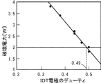
上記弾性表面波装置1において、IDT電極のデューティを変化させた場合の破壊電力の変化を図2に示す。図2において、デューティが0.5よりも小さくなると、破壊電力が大きくなっていくことが分かる。これは、電極指の幅寸法に比べて電極指間のギャップの寸法が大きくなることによる。そして、IDT電極のデューティを0.5未満、特に0.49以下とすることにより、破壊電力が絶対値として2W以上と大きくなることがわかる。携帯電話機の帯域フィルタとして用いられるような弾性表面波装置では、破壊電力は2W以上あることが求められる。従って、本発明では、IDT電極のデューティは、0.49以下とされている。
In the surface
もっとも、デューティを0.49以下、すなわち0.5よりも小さくすると、所望でないスプリアスが生じることがわかった。 However, it has been found that when the duty is 0.49 or less, that is, less than 0.5, unwanted spurious is generated.
しかしながら、このスプリアスはLiNbO3基板のオイラー角のθを下記の式(1)を満たす範囲とするように設定することにより抑圧することができる。However, this spurious can be suppressed by setting the Euler angle θ of the LiNbO 3 substrate to a range satisfying the following expression (1).
図3は、オイラー角(0°,θ,0°)のθが、82°、83°、84°または86°のLiNbO3基板上に、0.06λの膜厚のCuからなるIDT電極を形成し、第1の酸化ケイ素膜として、CuからなるIDT電極と同じ膜厚のSiO2膜を形成し、IDT電極及び第1の酸化ケイ素膜を覆うように、0.25λの厚みのSiO2膜を第2の酸化ケイ素膜として積層した構造におけるIDT電極のデューティとスプリアスとなるレイリー波の電気機械結合係数KR 2との関係を示す図である。FIG. 3 shows an IDT electrode made of Cu having a film thickness of 0.06λ on a LiNbO 3 substrate having an Euler angle (0 °, θ, 0 °) of 82 °, 83 °, 84 ° or 86 °. formed, as the first silicon oxide film, a SiO 2 film is formed having the same thickness as the IDT electrode made of Cu, so as to cover the IDT electrode and the first silicon oxide film, a thickness of 0.25 [lambda SiO 2 the membrane is a diagram showing the relationship between the electromechanical coupling coefficient K R 2 of the Rayleigh wave as a duty and spurious IDT electrodes in the laminated structure as a second silicon oxide film.
なお、図3及び後述の図4等における結果は、図6に示した計算モデルに基づいて有限要素法により計算した結果である。図6から明らかなように、無限の厚みのLiNbO3基板21上に、IDT電極22及び第1の酸化ケイ素膜23が形成されており、その上に第2の酸化ケイ素膜24が形成されている構造をモデルとした。Note that the results in FIG. 3 and FIG. 4 described later are the results calculated by the finite element method based on the calculation model shown in FIG. As is apparent from FIG. 6, the
図3から明らかなように、θ=82°では、デューティが0.5の場合に、レイリー波の電気機械結合係数KR 2は0.04%以下となっている。ところが、デューティが0.5より小さくなるに従って、レイリー波の電気機械結合係数KR 2が大きくなり、レイリー波によるスプリアスが無視できないことがわかる。従って、図3よりデューティが0.5より小さい場合には、オイラー角のθを調整する必要のあることがわかる。As is apparent from FIG. 3, at θ = 82 °, when the duty is 0.5, the Rayleigh wave electromechanical coupling coefficient K R 2 is 0.04% or less. However, it can be seen that as the duty becomes smaller than 0.5, the electromechanical coupling coefficient K R 2 of the Rayleigh wave increases and spurious due to the Rayleigh wave cannot be ignored. Therefore, it can be seen from FIG. 3 that when the duty is smaller than 0.5, it is necessary to adjust the Euler angle θ.
図4(a)は、オイラー角(0°,θ,0°)のLiNbO3基板に、上記と同様に、0.06λのCu膜からなるIDT電極を形成し、同じ膜厚のSiO2膜を形成した後に、0.25λの厚みのSiO2膜を形成した構造におけるレイリー波の電気機械結合係数KR 2が0.04%以下の領域を示す図である。図4(a)の斜線のハッチングを付している領域がレイリー波の電気機械結合係数KR 2が0.04%以下の領域である。また、図4(a)の縦方向に延びるデューティ=0.25の線は、デューティがこれ以上小さくなると、弾性表面波装置のIDT電極を実質的に製造することが困難な下限を示す。FIG. 4A shows a case in which an IDT electrode made of a Cu film of 0.06λ is formed on a LiNbO 3 substrate having Euler angles (0 °, θ, 0 °), and an SiO 2 film having the same film thickness. FIG. 6 is a diagram showing a region where the Rayleigh wave electromechanical coupling coefficient K R 2 is 0.04% or less in a structure in which a SiO 2 film having a thickness of 0.25λ is formed after forming. 4 electromechanical coefficient K R 2 regions are hatched in the hatching Rayleigh wave (a) is a region of 0.04% or less. Further, the line of duty = 0.25 extending in the vertical direction in FIG. 4A indicates a lower limit that makes it difficult to substantially manufacture the IDT electrode of the surface acoustic wave device when the duty is further reduced.
従って、図4(a)より、デューティが0.25以上、0.49以下である場合に、図4(a)のハッチングを付した領域にオイラー角のθを選択することにより、スプリアスとなるレイリー波の電気機械結合係数KR 2を0.04%以下と小さくすることができる。この図4(a)の斜線のハッチングを付した領域を、数式で示すと、式(2)で示す値となる。Therefore, from FIG. 4A, when the duty is 0.25 or more and 0.49 or less, selecting Euler angle θ in the hatched area of FIG. 4A results in spurious. the electromechanical coupling coefficient K R 2 of the Rayleigh wave can be reduced to 0.04% or less. When the hatched area in FIG. 4A is represented by a mathematical formula, the value is represented by the formula (2).
図4(b)に示すように、レイリー波の電気機械結合係数KR 2が0.04%以下となる領域は、CuからなるIDT電極の膜厚に依存する。従って、電極膜厚による依存性を考慮すると、式(2)は、前述した式(1)のように表すことができる。As shown in FIG. 4B, the region where the Rayleigh wave electromechanical coupling coefficient K R 2 is 0.04% or less depends on the film thickness of the IDT electrode made of Cu. Therefore, when the dependence due to the electrode film thickness is taken into consideration, the expression (2) can be expressed as the above-described expression (1).
なお、式(1)の関係は、第2の酸化ケイ素膜の膜厚が0.15λ〜0.4λの範囲では大きくは変化しない。これを、図5を参照して説明する。 Note that the relationship of the expression (1) does not change significantly when the thickness of the second silicon oxide film is in the range of 0.15λ to 0.4λ. This will be described with reference to FIG.
図5は、オイラー角(0°,θ,0°)のLiNbO3基板上に、0.06λの膜厚のCuからなるIDT電極をデューティ=0.50となるように形成した構造において、第2の酸化ケイ素膜の膜厚を0.20λ、0.25λまたは0.30λと変化させた場合のオイラー角のθと、レイリー波の電気機械結合係数KR 2との関係を示す図である。図5から明らかなように、SiO2の膜厚を0.20λ〜0.30λの範囲で変化させたとしても、オイラー角のθと、レイリー波の電気機械結合係数KR 2との関係は余り変化していないことがわかる。本願発明者の実験によれば、SiO2膜の膜厚を0.15λ〜0.40λの範囲で変化させた場合においても、図5に示した結果と同様に、レイリー波の電気機械結合係数KR 2と、θとの関係はほとんど変化しないことが確かめられている。FIG. 5 shows a structure in which an IDT electrode made of Cu having a film thickness of 0.06λ is formed on a LiNbO 3 substrate with Euler angles (0 °, θ, 0 °) so as to have a duty = 0.50. 2 is a graph showing the relationship between the Euler angle θ and the Rayleigh wave electromechanical coupling coefficient K R 2 when the thickness of the
なお、本発明においては、好ましくは、IDT電極の膜厚は、0.03λ〜0.072λの範囲とされる。すなわち、上述した式(1)によれば、Cuの膜厚が0.072λ付近で、θの上限値及び下限値が逆転することとなる。すなわち、0.072λを超えると、レイリー波の電気機械結合係数KR 2が0.04%以下になる範囲は存在しなくなる。従って、IDT電極の膜厚は、0.072λ以下が好ましい。In the present invention, the thickness of the IDT electrode is preferably in the range of 0.03λ to 0.072λ. That is, according to the above-described formula (1), the upper limit value and the lower limit value of θ are reversed when the film thickness of Cu is around 0.072λ. That is, if it exceeds 0.072λ, there is no range where the Rayleigh wave electromechanical coupling coefficient K R 2 is 0.04% or less. Therefore, the film thickness of the IDT electrode is preferably 0.072λ or less.
また、レイリー波のスプリアスについて考慮すると、IDT電極の膜厚が薄いほど、レイリー波の電気機械結合係数KR 2が小さくなる範囲は広がることになり、IDT電極の膜厚が薄ければ薄いほど望ましい。しかしながら、IDT電極の膜厚が薄過ぎると、弾性表面波の音速が遅い横波の音速よりも高くなり、減衰量が大きくなるおそれがある。この点を考慮すると、IDT電極の膜厚は、0.03λ以上であることが望ましい。従って、Cuを主体とするIDT電極の膜厚は、0.03λ〜0.072λの範囲が望ましい。In consideration for the spurious of the Rayleigh wave, as the thickness of the IDT electrode is thin, the electromechanical coefficient K R 2 decreases the range of the Rayleigh wave will be spread, as small as the thickness of the IDT electrode is thin desirable. However, if the film thickness of the IDT electrode is too thin, the acoustic velocity of the surface acoustic wave is higher than the acoustic velocity of the transverse wave, which may increase the attenuation. Considering this point, it is desirable that the film thickness of the IDT electrode is 0.03λ or more. Therefore, the film thickness of the IDT electrode mainly composed of Cu is preferably in the range of 0.03λ to 0.072λ.
次に、上記実施形態に基づき、実際に弾性表面波装置を作製した実施例を説明する。 Next, an example in which a surface acoustic wave device is actually manufactured based on the above embodiment will be described.
オイラー角(0°,82°〜86°,0°)の回転Y板X伝搬のLiNbO3基板を用意した。このLiNbO3基板上に、第1の酸化ケイ素膜として、SiO2膜を107nm(0.057λ)の厚みとなるように成膜した。しかる後、このSiO2膜上にレジストパターンを形成した後、該レジストパターンを用い反応性イオンエッチング(RIE)によりSiO2膜を選択的にエッチングし溝を形成した。この溝に、Cuを充填するように、Cu膜を成膜し、IDT電極を形成した。しかる後、IDT電極以外のCu膜を上記レジストパターンとともにリフトオフ法により除去した後、第2の酸化ケイ素膜として厚み460nm(0.24λ)のSiO2膜を成膜した。A LiNbO 3 substrate for propagating a rotating Y plate X with Euler angles (0 °, 82 ° to 86 °, 0 °) was prepared. On this LiNbO 3 substrate, a SiO 2 film was formed as a first silicon oxide film to a thickness of 107 nm (0.057λ). Then, this was formed a resist pattern on the SiO 2 film was formed on a selectively etched grooves of the SiO 2 film by reactive ion etching using the resist pattern (RIE). A Cu film was formed to fill the groove with Cu, thereby forming an IDT electrode. Thereafter, the Cu film other than the IDT electrode was removed together with the resist pattern by a lift-off method, and a SiO 2 film having a thickness of 460 nm (0.24λ) was formed as a second silicon oxide film.
このようにして、λ=1.89μm、すなわち1.9GHz帯の共振周波数を有する1ポート型弾性表面波共振子を作製した。 In this way, a 1-port surface acoustic wave resonator having a resonance frequency of λ = 1.89 μm, that is, a 1.9 GHz band was manufactured.
図7及び図8に、上記のようにして得られた1ポート型弾性表面波共振子のインピーダンス−周波数特性及び位相−周波数特性を示す。図7では、オイラー角のθが82°であり、IDT電極のデューティが0.3、0.4または0.5の場合の結果が示されており、図8では、オイラー角のθが86°であり、デューティが0.3、0.4または0.5の場合の特性が示されている。 7 and 8 show the impedance-frequency characteristics and phase-frequency characteristics of the 1-port surface acoustic wave resonator obtained as described above. FIG. 7 shows the results when the Euler angle θ is 82 ° and the duty of the IDT electrode is 0.3, 0.4, or 0.5. In FIG. 8, the Euler angle θ is 86. The characteristics are shown for ° and the duty is 0.3, 0.4 or 0.5.
図7から明らかなように、オイラー角のθ=82°の場合には、デューティ=0.5で消えていたスプリアスが、デューティが0.4あるいは0.3と小さくなるに従って、矢印X1,X2で示すように、スプリアスが大きく現れていることがわかる。 As is apparent from FIG. 7, in the case of the Euler angle θ = 82 °, the spurious that disappeared at the duty = 0.5 decreases as the duty becomes 0.4 or 0.3, and the arrows X1, X2 As can be seen, a large amount of spurious appears.
これに対して、図8から明らかなように、オイラー角のθが86°の場合には、デューティ=0.5で現れていた矢印Yで示すスプリアスが、デューティが小さくなるに従って、小さくなっていることがわかる。この場合、θ=86°かつデューティ=0.3の場合が、上述した式(1)を満たす範囲であり、他の場合は、上述した式(1)を満たさない範囲、すなわち本発明の範囲外の例である。 On the other hand, as is clear from FIG. 8, when Euler angle θ is 86 °, the spurious indicated by arrow Y that appeared at duty = 0.5 becomes smaller as the duty becomes smaller. I understand that. In this case, the case where θ = 86 ° and the duty = 0.3 is a range satisfying the above-described expression (1). In other cases, the range not satisfying the above-described expression (1), that is, the scope of the present invention. It is an outside example.
従って、図7及び図8の結果からも明らかなように、上述した式(1)を満たすようにオイラー角のθをデューティDを考慮して設定することにより、SH波を利用した場合の所望でないスプリアスを効果的に抑圧し得ることがわかる。 Therefore, as is apparent from the results of FIGS. 7 and 8, the desired value when the SH wave is used by setting the Euler angle θ in consideration of the duty D so as to satisfy the above-described equation (1). It can be seen that spurious noise can be effectively suppressed.
なお、IDT電極は、Cuを主体とする限り、Cuからなる電極層の下方に下地膜としての密着層が積層されていてもよく、あるいは主たる電極層の上面に、保護層が積層されていてよい。さらに、主たる電極層についても、Cu単体からなる必要は必ずしもなく、Cuを主体とする合金から構成されていてもよい。また、CuやCuを主体とする合金からなる電極膜に、他の金属からなる従たる金属膜が積層されていてもよい。 As long as Cu is mainly used for the IDT electrode, an adhesion layer as a base film may be laminated below the electrode layer made of Cu, or a protective layer is laminated on the upper surface of the main electrode layer. Good. Further, the main electrode layer is not necessarily made of Cu alone, and may be made of an alloy mainly composed of Cu. Further, a subordinate metal film made of another metal may be laminated on an electrode film made of Cu or an alloy mainly containing Cu.
次に、上記実施例と同様にして、WCDMA用のデュプレクサDPXを作製した。ここでは、デュプレクサDPXの送信側帯域フィルタを、本発明に従って構成された弾性表面波共振子を複数用いた弾性表面波フィルタにより作製した。より具体的には、オイラー角(0°,84°0°)のLiNbO3基板上に、膜厚108nm(0.057λ)及びデューティ=0.40となるようにCuからなるIDT電極を形成した。なお、IDT電極と等しい膜厚のSiO2膜を第1の酸化ケイ素膜として成膜し、IDT電極及び第1の酸化ケイ素膜を覆うように、厚みを159nm(0.24λ)のSiO2膜を第2の酸化ケイ素膜として形成した。ここでは、さらに、最上部に、周波数調整するために、SiN膜を成膜し、SiN膜をエッチングすることにより、周波数を調整した。周波数調整後のSiN膜の膜厚は約15nm程度である。Next, a duplexer DPX for WCDMA was produced in the same manner as in the above example. Here, the transmission-side band filter of the duplexer DPX was produced by a surface acoustic wave filter using a plurality of surface acoustic wave resonators configured according to the present invention. More specifically, an IDT electrode made of Cu was formed on a LiNbO 3 substrate with Euler angles (0 °, 84 ° 0 °) so as to have a film thickness of 108 nm (0.057λ) and a duty = 0.40. . Incidentally, by forming a IDT electrode is equal to the thickness of the SiO 2 film as the first silicon oxide film, so as to cover the IDT electrode and the first silicon oxide film, SiO 2 film of 159nm thickness (0.24λ) Was formed as a second silicon oxide film. Here, in order to further adjust the frequency, an SiN film was formed at the top, and the frequency was adjusted by etching the SiN film. The film thickness of the SiN film after frequency adjustment is about 15 nm.
なお、周波数調整膜としては、SiN膜の他、SiC膜やSi膜などを用いてもよい。 As the frequency adjustment film, a SiC film, a Si film, or the like may be used in addition to the SiN film.
図9は、このようにして得られたDPXの弾性表面波フィルタのフィルタ特性を示す図である。比較のために、図9に、破線により、オイラー角が(0°,82°,0°)とされていることを除いては、上記と同様に構成されたデュプレクサの弾性表面波フィルタのフィルタ特性を示す。なお、実線で示す特性、すなわちオイラー角(0°,84°,0°)と、上記膜厚及び膜厚のCuからなるIDT電極は、式(1)を満たしており、他方、破線で示すフィルタ特性の場合には、式(1)に示す関係は満たされていない。図9から明らかなように、破線で示す比較例では、矢印Z1,Z2で示す大きなスプリアスが現れている。これは、レイリー波によるスプリアスである。これに対して、第2の実施例では、このようなスプリアスが十分に抑圧されており、従って、良好なフィルタ特性の得られることがわかる。 FIG. 9 is a diagram showing the filter characteristics of the DPX surface acoustic wave filter obtained as described above. For comparison, a duplexer surface acoustic wave filter constructed in the same manner as above except that the Euler angles are set to (0 °, 82 °, 0 °) by broken lines in FIG. Show properties. Note that the characteristic indicated by the solid line, that is, the Euler angles (0 °, 84 °, 0 °) and the IDT electrode made of Cu having the above film thickness satisfy the formula (1), and on the other hand, it is indicated by the broken line. In the case of the filter characteristic, the relationship shown in Expression (1) is not satisfied. As can be seen from FIG. 9, in the comparative example indicated by the broken line, large spurs indicated by arrows Z1 and Z2 appear. This is spurious due to Rayleigh waves. On the other hand, in the second embodiment, it can be seen that such spurious noise is sufficiently suppressed, and therefore good filter characteristics can be obtained.
次に、上記実施例2で作製したデュプレクサTPXの弾性表面波フィルタの通過帯域及び通過帯域よりも高域側の周波数領域の特性を図10に示す。 Next, FIG. 10 shows the passband of the surface acoustic wave filter of the duplexer TPX produced in Example 2 and the characteristics of the frequency region higher than the passband.
また、比較のために、第2の酸化ケイ素膜の膜厚を、0.35λに変更したことを除いては、上記第2の実施例と同様にして構成された弾性表面波フィルタの周波数特性を図11に示す。 For comparison, the frequency characteristics of a surface acoustic wave filter configured in the same manner as in the second embodiment except that the thickness of the second silicon oxide film is changed to 0.35λ. Is shown in FIG.
図11では、矢印Wで示すように、SH波の高次モードによるスプリアスが大きく現れている。すなわち、SH波の高次モードによるとみられるスプリアスは、第2の酸化ケイ素膜としてのSiO2膜の膜厚に大きく依存することがわかる。そして、フィルタ特性上、第2の酸化ケイ素膜の膜厚を0.03λ以下とした場合には、図11に矢印Wで示すSH波の高次モードによるスプリアスを効果的に抑圧することができ、望ましい。In FIG. 11, as indicated by the arrow W, spurious due to the higher order mode of the SH wave appears greatly. That is, it can be seen that the spurious that appears to be due to the higher order mode of the SH wave greatly depends on the thickness of the SiO 2 film as the second silicon oxide film. If the thickness of the second silicon oxide film is 0.03λ or less due to the filter characteristics, it is possible to effectively suppress the spurious due to the higher order mode of the SH wave indicated by the arrow W in FIG. ,desirable.
LiNbO3基板のオイラー角は、上記実施形態では、(0°,θ±5°,0°)とされていたが、本願発明者の実験によれば、オイラー角(φ,θ,ψ)におけるφは0°±5°の範囲であればよく、ψは0°±10°の範囲であればよく、いずれの場合においても、上記実施形態と同様の効果が得られることが確認されている。In the above embodiment, the Euler angles of the LiNbO 3 substrate are (0 °, θ ± 5 °, 0 °), but according to the experiments by the inventors of the present application, the Euler angles (φ, θ, ψ) φ only needs to be in the range of 0 ° ± 5 °, and ψ only needs to be in the range of 0 ° ± 10 °. In any case, it has been confirmed that the same effect as the above embodiment can be obtained. .
さらに、前述した1ポート型弾性表面波共振子やデュプレクサの帯域フィルタ部に限らず、様々な共振子や様々な回路構成の表面波フィルタに本発明を適用することができる。 Furthermore, the present invention can be applied not only to the above-described 1-port surface acoustic wave resonator and duplexer bandpass filter but also to various resonators and surface wave filters having various circuit configurations.
Claims (2)
前記LiNbO3基板上に形成されており、Cuを主体とするIDT電極を含む電極と、
前記電極が形成されている領域を除いた残りの領域において、前記電極と等しい厚みとなるように形成されている第1の酸化ケイ素膜と、
前記電極及び第1の酸化ケイ素膜を被覆するように形成された第2の酸化ケイ素膜とを備え、SH波を利用した弾性表面波装置であって、
前記IDT電極のデューティDが0.49以下であり、かつ前記オイラー角(0°±5°,θ±5°,0°±10°)のθが、IDT電極のデューティD及びIDT電極膜厚を波長で規格化した値であるCとの間に、下記の式(1)を満たす範囲とされていることを特徴とする、弾性表面波装置。
An electrode including an IDT electrode mainly composed of Cu, formed on the LiNbO 3 substrate;
A first silicon oxide film formed to have the same thickness as the electrode in the remaining region excluding the region where the electrode is formed;
A surface acoustic wave device using SH waves, comprising the electrode and a second silicon oxide film formed so as to cover the first silicon oxide film,
The duty D of the IDT electrode is 0.49 or less, and θ of the Euler angles (0 ° ± 5 °, θ ± 5 °, 0 ° ± 10 °) is the duty D of the IDT electrode and the IDT electrode film thickness. The surface acoustic wave device is characterized by being in a range satisfying the following formula (1) between C and C, which is a value normalized by wavelength .
Priority Applications (1)
| Application Number | Priority Date | Filing Date | Title |
|---|---|---|---|
| JP2008521129A JP5137828B2 (en) | 2006-06-16 | 2007-05-22 | Surface acoustic wave device |
Applications Claiming Priority (4)
| Application Number | Priority Date | Filing Date | Title |
|---|---|---|---|
| JP2006167303 | 2006-06-16 | ||
| JP2006167303 | 2006-06-16 | ||
| PCT/JP2007/060413 WO2007145057A1 (en) | 2006-06-16 | 2007-05-22 | Surface acoustic wave device |
| JP2008521129A JP5137828B2 (en) | 2006-06-16 | 2007-05-22 | Surface acoustic wave device |
Publications (2)
| Publication Number | Publication Date |
|---|---|
| JPWO2007145057A1 JPWO2007145057A1 (en) | 2009-10-29 |
| JP5137828B2 true JP5137828B2 (en) | 2013-02-06 |
Family
ID=38831577
Family Applications (1)
| Application Number | Title | Priority Date | Filing Date |
|---|---|---|---|
| JP2008521129A Active JP5137828B2 (en) | 2006-06-16 | 2007-05-22 | Surface acoustic wave device |
Country Status (4)
| Country | Link |
|---|---|
| US (1) | US7804221B2 (en) |
| JP (1) | JP5137828B2 (en) |
| DE (1) | DE112007001426B4 (en) |
| WO (1) | WO2007145057A1 (en) |
Families Citing this family (11)
| Publication number | Priority date | Publication date | Assignee | Title |
|---|---|---|---|---|
| JP4968334B2 (en) * | 2007-06-06 | 2012-07-04 | 株式会社村田製作所 | Surface acoustic wave device |
| WO2009090715A1 (en) * | 2008-01-17 | 2009-07-23 | Murata Manufacturing Co., Ltd. | Surface acoustic wave device |
| JP2010193429A (en) | 2009-01-26 | 2010-09-02 | Murata Mfg Co Ltd | Acoustic wave device |
| JP5579429B2 (en) * | 2009-12-15 | 2014-08-27 | 太陽誘電株式会社 | Elastic wave device, communication module, communication device |
| DE102010034121A1 (en) | 2010-08-12 | 2012-02-16 | Epcos Ag | Working with acoustic waves device with reduced temperature response of the frequency position and method of manufacture |
| KR101623099B1 (en) * | 2010-12-24 | 2016-05-20 | 가부시키가이샤 무라타 세이사쿠쇼 | Elastic wave device and production method thereof |
| CN103283147B (en) * | 2010-12-24 | 2016-09-21 | 株式会社村田制作所 | Acoustic wave device and manufacture method thereof |
| JP6388029B2 (en) * | 2014-06-26 | 2018-09-12 | 株式会社村田製作所 | Longitudinal coupled resonator type surface acoustic wave filter |
| JP6652221B2 (en) * | 2017-04-17 | 2020-02-19 | 株式会社村田製作所 | Elastic wave device, high-frequency front-end circuit, and communication device |
| JP2019145895A (en) * | 2018-02-16 | 2019-08-29 | 株式会社村田製作所 | Acoustic wave device, multiplexer, high frequency front end circuit and communication apparatus |
| DE102018113624A1 (en) * | 2018-06-07 | 2019-12-12 | RF360 Europe GmbH | An electroacoustic resonator and RF filter comprising an electroacoustic resonator |
Citations (5)
| Publication number | Priority date | Publication date | Assignee | Title |
|---|---|---|---|---|
| JP2001036378A (en) * | 1999-07-16 | 2001-02-09 | Mitsubishi Electric Corp | Elastic wave device |
| JP2003008390A (en) * | 2001-04-16 | 2003-01-10 | Murata Mfg Co Ltd | Surface acoustic wave device and communication equipment |
| JP2003249835A (en) * | 2001-04-16 | 2003-09-05 | Murata Mfg Co Ltd | Surface acoustic wave device and communication device |
| WO2004070946A1 (en) * | 2003-02-10 | 2004-08-19 | Murata Manufacturing Co., Ltd. | Elastic boundary wave device |
| WO2005034347A1 (en) * | 2003-10-03 | 2005-04-14 | Murata Manufacturing Co., Ltd. | Surface acoustic wave device |
Family Cites Families (3)
| Publication number | Priority date | Publication date | Assignee | Title |
|---|---|---|---|---|
| TW241397B (en) * | 1993-01-14 | 1995-02-21 | Murata Manufacturing Co | |
| JPWO2005011117A1 (en) | 2003-07-29 | 2006-09-14 | 株式会社村田製作所 | 1-port surface acoustic wave resonator and surface acoustic wave filter |
| WO2005036743A1 (en) * | 2003-10-10 | 2005-04-21 | Murata Manufacturing Co., Ltd. | Boundary acoustic wave device |
-
2007
- 2007-05-22 WO PCT/JP2007/060413 patent/WO2007145057A1/en not_active Ceased
- 2007-05-22 JP JP2008521129A patent/JP5137828B2/en active Active
- 2007-05-22 DE DE112007001426.1T patent/DE112007001426B4/en active Active
-
2008
- 2008-12-11 US US12/332,394 patent/US7804221B2/en active Active
Patent Citations (5)
| Publication number | Priority date | Publication date | Assignee | Title |
|---|---|---|---|---|
| JP2001036378A (en) * | 1999-07-16 | 2001-02-09 | Mitsubishi Electric Corp | Elastic wave device |
| JP2003008390A (en) * | 2001-04-16 | 2003-01-10 | Murata Mfg Co Ltd | Surface acoustic wave device and communication equipment |
| JP2003249835A (en) * | 2001-04-16 | 2003-09-05 | Murata Mfg Co Ltd | Surface acoustic wave device and communication device |
| WO2004070946A1 (en) * | 2003-02-10 | 2004-08-19 | Murata Manufacturing Co., Ltd. | Elastic boundary wave device |
| WO2005034347A1 (en) * | 2003-10-03 | 2005-04-14 | Murata Manufacturing Co., Ltd. | Surface acoustic wave device |
Also Published As
| Publication number | Publication date |
|---|---|
| DE112007001426T5 (en) | 2009-04-23 |
| US7804221B2 (en) | 2010-09-28 |
| DE112007001426B4 (en) | 2014-02-13 |
| JPWO2007145057A1 (en) | 2009-10-29 |
| WO2007145057A1 (en) | 2007-12-21 |
| US20090085429A1 (en) | 2009-04-02 |
Similar Documents
| Publication | Publication Date | Title |
|---|---|---|
| JP5137828B2 (en) | Surface acoustic wave device | |
| JP4636179B2 (en) | Surface acoustic wave device | |
| JP3885824B2 (en) | Surface acoustic wave device | |
| JP4793448B2 (en) | Boundary acoustic wave device | |
| JP5213708B2 (en) | Manufacturing method of surface acoustic wave device | |
| US20080303379A1 (en) | Surface acoustic wave device | |
| US8680744B2 (en) | Surface acoustic wave device | |
| CN102204094B (en) | Elastic wave element and electronic device using the same | |
| WO2020204045A1 (en) | High-order mode surface acoustic wave device | |
| JP4636178B2 (en) | Surface acoustic wave device | |
| JP2004254291A (en) | Acoustic surface wave device | |
| CN101485086A (en) | Surface Acoustic Wave Device | |
| JPWO2007099742A1 (en) | Elastic wave device and manufacturing method thereof | |
| CN101517893A (en) | Boundary acoustic wave device | |
| JP5163805B2 (en) | Surface acoustic wave device and manufacturing method thereof | |
| JP4297139B2 (en) | Surface acoustic wave device | |
| JP5110091B2 (en) | Surface acoustic wave device | |
| JPWO2009090715A1 (en) | Surface acoustic wave device | |
| JP4967393B2 (en) | Surface acoustic wave device |
Legal Events
| Date | Code | Title | Description |
|---|---|---|---|
| A131 | Notification of reasons for refusal |
Free format text: JAPANESE INTERMEDIATE CODE: A131 Effective date: 20110118 |
|
| A521 | Request for written amendment filed |
Free format text: JAPANESE INTERMEDIATE CODE: A523 Effective date: 20110318 |
|
| A02 | Decision of refusal |
Free format text: JAPANESE INTERMEDIATE CODE: A02 Effective date: 20110517 |
|
| A01 | Written decision to grant a patent or to grant a registration (utility model) |
Free format text: JAPANESE INTERMEDIATE CODE: A01 |
|
| A61 | First payment of annual fees (during grant procedure) |
Free format text: JAPANESE INTERMEDIATE CODE: A61 Effective date: 20121113 |
|
| R150 | Certificate of patent or registration of utility model |
Ref document number: 5137828 Country of ref document: JP Free format text: JAPANESE INTERMEDIATE CODE: R150 Free format text: JAPANESE INTERMEDIATE CODE: R150 |
|
| FPAY | Renewal fee payment (event date is renewal date of database) |
Free format text: PAYMENT UNTIL: 20151122 Year of fee payment: 3 |