EP2741062B1 - Method for measuring temperature of semiconductor layer - Google Patents
Method for measuring temperature of semiconductor layer Download PDFInfo
- Publication number
- EP2741062B1 EP2741062B1 EP11870369.3A EP11870369A EP2741062B1 EP 2741062 B1 EP2741062 B1 EP 2741062B1 EP 11870369 A EP11870369 A EP 11870369A EP 2741062 B1 EP2741062 B1 EP 2741062B1
- Authority
- EP
- European Patent Office
- Prior art keywords
- semiconductor layer
- temperature
- light
- wavelength
- laser beam
- Prior art date
- Legal status (The legal status is an assumption and is not a legal conclusion. Google has not performed a legal analysis and makes no representation as to the accuracy of the status listed.)
- Active
Links
- 239000004065 semiconductor Substances 0.000 title claims description 172
- 238000000034 method Methods 0.000 title claims description 23
- 230000007423 decrease Effects 0.000 claims description 57
- 230000008021 deposition Effects 0.000 claims description 39
- 238000002834 transmittance Methods 0.000 claims description 24
- 230000003746 surface roughness Effects 0.000 claims description 19
- 230000003287 optical effect Effects 0.000 claims description 7
- 238000005259 measurement Methods 0.000 claims 1
- 239000010410 layer Substances 0.000 description 148
- 239000000758 substrate Substances 0.000 description 65
- 238000000151 deposition Methods 0.000 description 43
- 238000012544 monitoring process Methods 0.000 description 12
- 230000005540 biological transmission Effects 0.000 description 9
- 238000010438 heat treatment Methods 0.000 description 7
- 238000010586 diagram Methods 0.000 description 6
- 230000001276 controlling effect Effects 0.000 description 5
- 239000011521 glass Substances 0.000 description 5
- 239000000463 material Substances 0.000 description 5
- 229910002601 GaN Inorganic materials 0.000 description 4
- JMASRVWKEDWRBT-UHFFFAOYSA-N Gallium nitride Chemical compound [Ga]#N JMASRVWKEDWRBT-UHFFFAOYSA-N 0.000 description 4
- 238000005229 chemical vapour deposition Methods 0.000 description 4
- 238000001514 detection method Methods 0.000 description 4
- 230000002596 correlated effect Effects 0.000 description 3
- 238000001451 molecular beam epitaxy Methods 0.000 description 3
- 229910017083 AlN Inorganic materials 0.000 description 2
- 229910001218 Gallium arsenide Inorganic materials 0.000 description 2
- 238000009529 body temperature measurement Methods 0.000 description 2
- 239000013078 crystal Substances 0.000 description 2
- 206010034972 Photosensitivity reaction Diseases 0.000 description 1
- 230000000052 comparative effect Effects 0.000 description 1
- 239000000470 constituent Substances 0.000 description 1
- 230000000875 corresponding effect Effects 0.000 description 1
- 230000001419 dependent effect Effects 0.000 description 1
- 238000005137 deposition process Methods 0.000 description 1
- 230000000694 effects Effects 0.000 description 1
- 230000008020 evaporation Effects 0.000 description 1
- 238000001704 evaporation Methods 0.000 description 1
- 230000006870 function Effects 0.000 description 1
- 229910052736 halogen Inorganic materials 0.000 description 1
- 150000002367 halogens Chemical class 0.000 description 1
- 230000002452 interceptive effect Effects 0.000 description 1
- 230000001678 irradiating effect Effects 0.000 description 1
- 230000036211 photosensitivity Effects 0.000 description 1
- 238000001055 reflectance spectroscopy Methods 0.000 description 1
- 229910052594 sapphire Inorganic materials 0.000 description 1
- 239000010980 sapphire Substances 0.000 description 1
- 230000035945 sensitivity Effects 0.000 description 1
- 239000002356 single layer Substances 0.000 description 1
- 239000012780 transparent material Substances 0.000 description 1
Images


Classifications
-
- G—PHYSICS
- G01—MEASURING; TESTING
- G01K—MEASURING TEMPERATURE; MEASURING QUANTITY OF HEAT; THERMALLY-SENSITIVE ELEMENTS NOT OTHERWISE PROVIDED FOR
- G01K11/00—Measuring temperature based upon physical or chemical changes not covered by groups G01K3/00, G01K5/00, G01K7/00 or G01K9/00
- G01K11/12—Measuring temperature based upon physical or chemical changes not covered by groups G01K3/00, G01K5/00, G01K7/00 or G01K9/00 using changes in colour, translucency or reflectance
- G01K11/18—Measuring temperature based upon physical or chemical changes not covered by groups G01K3/00, G01K5/00, G01K7/00 or G01K9/00 using changes in colour, translucency or reflectance of materials which change translucency
-
- C—CHEMISTRY; METALLURGY
- C23—COATING METALLIC MATERIAL; COATING MATERIAL WITH METALLIC MATERIAL; CHEMICAL SURFACE TREATMENT; DIFFUSION TREATMENT OF METALLIC MATERIAL; COATING BY VACUUM EVAPORATION, BY SPUTTERING, BY ION IMPLANTATION OR BY CHEMICAL VAPOUR DEPOSITION, IN GENERAL; INHIBITING CORROSION OF METALLIC MATERIAL OR INCRUSTATION IN GENERAL
- C23C—COATING METALLIC MATERIAL; COATING MATERIAL WITH METALLIC MATERIAL; SURFACE TREATMENT OF METALLIC MATERIAL BY DIFFUSION INTO THE SURFACE, BY CHEMICAL CONVERSION OR SUBSTITUTION; COATING BY VACUUM EVAPORATION, BY SPUTTERING, BY ION IMPLANTATION OR BY CHEMICAL VAPOUR DEPOSITION, IN GENERAL
- C23C16/00—Chemical coating by decomposition of gaseous compounds, without leaving reaction products of surface material in the coating, i.e. chemical vapour deposition [CVD] processes
- C23C16/44—Chemical coating by decomposition of gaseous compounds, without leaving reaction products of surface material in the coating, i.e. chemical vapour deposition [CVD] processes characterised by the method of coating
- C23C16/52—Controlling or regulating the coating process
-
- C—CHEMISTRY; METALLURGY
- C30—CRYSTAL GROWTH
- C30B—SINGLE-CRYSTAL GROWTH; UNIDIRECTIONAL SOLIDIFICATION OF EUTECTIC MATERIAL OR UNIDIRECTIONAL DEMIXING OF EUTECTOID MATERIAL; REFINING BY ZONE-MELTING OF MATERIAL; PRODUCTION OF A HOMOGENEOUS POLYCRYSTALLINE MATERIAL WITH DEFINED STRUCTURE; SINGLE CRYSTALS OR HOMOGENEOUS POLYCRYSTALLINE MATERIAL WITH DEFINED STRUCTURE; AFTER-TREATMENT OF SINGLE CRYSTALS OR A HOMOGENEOUS POLYCRYSTALLINE MATERIAL WITH DEFINED STRUCTURE; APPARATUS THEREFOR
- C30B25/00—Single-crystal growth by chemical reaction of reactive gases, e.g. chemical vapour-deposition growth
- C30B25/02—Epitaxial-layer growth
- C30B25/16—Controlling or regulating
-
- G—PHYSICS
- G01—MEASURING; TESTING
- G01K—MEASURING TEMPERATURE; MEASURING QUANTITY OF HEAT; THERMALLY-SENSITIVE ELEMENTS NOT OTHERWISE PROVIDED FOR
- G01K7/00—Measuring temperature based on the use of electric or magnetic elements directly sensitive to heat ; Power supply therefor, e.g. using thermoelectric elements
- G01K7/01—Measuring temperature based on the use of electric or magnetic elements directly sensitive to heat ; Power supply therefor, e.g. using thermoelectric elements using semiconducting elements having PN junctions
-
- H—ELECTRICITY
- H01—ELECTRIC ELEMENTS
- H01L—SEMICONDUCTOR DEVICES NOT COVERED BY CLASS H10
- H01L21/00—Processes or apparatus adapted for the manufacture or treatment of semiconductor or solid state devices or of parts thereof
- H01L21/67—Apparatus specially adapted for handling semiconductor or electric solid state devices during manufacture or treatment thereof; Apparatus specially adapted for handling wafers during manufacture or treatment of semiconductor or electric solid state devices or components ; Apparatus not specifically provided for elsewhere
- H01L21/67005—Apparatus not specifically provided for elsewhere
- H01L21/67242—Apparatus for monitoring, sorting or marking
- H01L21/67248—Temperature monitoring
Definitions
- the wavelength of the first laser beam L1 is selected such that the temperature of the semiconductor layer 7 is T3 at a decrease starting point (e) and T4 at a decrease ending point (f).
- the wavelength of the second laser beam L2 is selected such that the temperature is T5 at a decrease starting point (g) and T6 at a decrease ending point (h).
- the range from the temperature T3 to T4 is a first temperature range in which the light transmission quantity of the first laser beam L1 decreases, while the range from the temperature T5 to T6 is a second temperature range in which the light transmission quantity of the second laser beam L2 decreases.
- the second temperature range is higher than the first temperature range.
- both maximum of detected light quantity associated with the first laser beam L1 and the second laser beam L2 become D4, as shown in Fig. 7 , and in the same way, the decrease of light quantity of the first laser beam L1 and the decrease of light quantity of the second laser beam L2 are equal and become (D4 - D3).
- Another example of calibration is as follows. In the case where the semiconductor layer 7 has not been deposited on the transparent substrate 6 in the chamber 2, the laser beam is emitted from the first laser beam source 22 shown in Fig.2 and the diffused reflection of the first laser beam L1 from the bottom surface 6a of the substrate 6 and from the surface of the substrate 6 is detected by the light receiver 11. Then, the laser beam is emitted from the second laser beam source 23 and the diffused reflection of the second laser beam L2 from the bottom surface 6a of the substrate 6 and from the surface of the substrate 6 is detected by the light receiver 11. Finally, the calibration is performed by software or hardware adjustments such that the light quantity detected when the laser beam is emitted from the first laser beam source 22 becomes equal to the light quantity detected when the laser beam is emitted from the second laser beam source 23.
- the temperature of the semiconductor layer 7 can be controlled to be the temperature Ty between the temperatures T5 and T6 by monitoring the temperature after the second laser beam L2 has passed through the decrease starting point (g).
- the temperature of the semiconductor layer 7 can be maintained at an optimum temperature Ty for deposition in the second temperature range (T5 - T6) by controlling the heater 3a with the heating controller 31 and keeping the monitored value of the detected light quantity at Dc.
- the temperature of the semiconductor layer 7 can be maintained at the optimum temperature Ty for deposition by monitoring the detected light quantity of the second laser beam L2 without the need to raise the temperature of the semiconductor layer 7 above the second temperature range.
Description
- The present invention relates to a method and an apparatus for measuring the temperature of a semiconductor layer by which, when a semiconductor layer of a light-emitting diode or other semiconductor devices is formed by deposition, the temperature or surface roughness of the semiconductor layer can be measured during or after deposition.
- Semiconductors such as AlN, GaAs, GaN, InP, Si and SiC can be formed by deposition. Examples of deposition techniques include chemical vapor deposition (CVD) and molecular beam epitaxy (MBE). In such a deposition technique, a film can be formed such that a substrate is placed in an evacuated chamber and source molecules are supplied in the form of a source gas onto the substrate to deposit a crystal layer on the surface of the substrate.
- In deposition techniques of this type, the temperature of the substrate in the chamber has to be accurately controlled in order to form a high purity, high density, reproducible semiconductor crystal layer at a constant deposition rate. To this end, a monitor for measuring the temperature of the substrate in the chamber is provided along with a heater for heating the substrate, so that the heating temperature of the heater can be controlled based on the temperature measured by the monitor.
- Conventionally, as described in
Patent Literatures - When the infrared light emitted from the surface of the heated substrate passes through the semiconductor layer during deposition, a light passing through the semiconductor layer interferes with a light reflected inside the semiconductor layer to cause minor fluctuations of the detection output from the pyrometer, and moreover, the degree of interference varies with a change in the film thickness of the semiconductor layer during deposition. Conventionally, this problem has been solved by disposing a light emitting device outside the chamber, applying a laser light to the semiconductor layer during deposition through the glass window of the chamber, and monitoring a laser light passing through the semiconductor layer. Since the laser light passing through the semiconductor layer also interferes with a laser light reflected inside the semiconductor layer, as with the case of the infrared lights, the output fluctuations of the monitored laser light due to the interference can be used for calibration to eliminate or reduce the interference with the infrared light to be detected by the pyrometer.
- However, even if the interference with the infrared light to be detected by the pyrometer can be avoided, the temperature monitoring is performed by the pyrometer at a place away from the surface of the substrate, generally, outside of the chamber through a glass window. Since not only a long distance but also the glass window exists between the substrate surface from which heat is actually emitted and the monitoring spot, it is inevitable that an error will arise between the temperature measured by the pyrometer and the actual temperature of the substrate surface.
- If the semiconductor layer growing on the surface of the substrate is transparent, moreover, the pyrometer actually measures the temperature of the substrate surface through the transparent semiconductor layer. Thus, it is difficult to directly and accurately measure the temperature of the growing semiconductor layer itself by a measuring method with a pyrometer.
-
Patent Literature 1 cited below further discloses the use of a thermocouple monitor for measuring the temperature of the substrate at its back side. However, since the thermocouple monitor is disposed on the back side of the substrate, it is impossible to accurately measure the actual temperature of the substrate surface. In addition, since the thermocouple monitor cannot readily respond to a temperature change in the chamber because of its large heat capacity, it is difficult to accurately measure the temperature of the substrate. -
Patent Literature 3 cited below further discloses a technique of irradiating a light from a halogen lamp on a wafer to be measured and calculating the surface temperature of the wafer from transmittance, reflectance and wavelength of the light. - However, since transmittance and reflectance of light vary greatly depending on various factors such as surface roughness of the wafer, it is difficult to determine the temperature of the object to be measured with high accuracy only from transmittance and reflectance of a single light.
-
- Patent Literature 1: Japanese Unexamined Patent Application Publication No.
2001-289714 - Patent Literature 2: Japanese Unexamined Patent Application Publication No.
2002-367907 - Patent Literature 3: Japanese Unexamined Patent Application Publication No.
2002-122480 - S.R.Johnson: "Semiconductor substrate temperature measurement by diffuse reflectance spectroscopy in molecular beam epitaxy", Journal of Vacuum Sciene and Technology B, , and
US 5741070A1 disclose temperature measurement methods. - The present invention is to solve the above-mentioned problems of the prior art and has an object to provide a method and an apparatus for measuring the temperature of a semiconductor layer by and with which the temperature of the semiconductor layer can be accurately determined during or after deposition onto a substrate, enabling deposition of a high-quality semiconductor layer.
- It is another object of the present invention to provide a method and an apparatus for measuring a temperature of a semiconductor layer by which a change in the temperature of the semiconductor layer can be immediately detected by monitoring a change in the quantity of light passing through the semiconductor layer.
- It is still another object of the present invention to provide a method and an apparatus for measuring a temperature of a semiconductor layer by which whether a change in the detected light quantity is due to a change in the temperature of the semiconductor layer or other factors can be determined based on a change in the light quantity detected by applying lights of different wavelengths to the semiconductor layer.
- According to a first aspect of the present invention, there is provided a method for measuring a temperature of a semiconductor laser as claimed in
claim 1. Other features are set out in the dependent claims and the following description. - With the temperature measuring method and apparatus according to the present invention, the temperature of the semiconductor layer can be immediately determined by applying lights of different wavelengths to the semiconductor layer during or after deposition.
- Moreover, whether a change in the detected light quantity is due to a change in the temperature of the semiconductor layer or other factors can be determined based on a change in the light quantity detected by applying lights of different wavelengths to the semiconductor layer. This makes it possible to determine whether there is a change in the surface roughness of the semiconductor layer during deposition and also to determine the degree of surface roughness.
-
-
Fig. 1 A schematic explanatory drawing showing the configuration of a film deposition apparatus and a temperature measuring apparatus according to a first embodiment of the present invention; -
Fig. 2 An explanatory drawing showing details of a light emitting device in the temperature measuring apparatus; -
Fig. 3 An explanatory drawing showing details of a light detecting device in the temperature measuring apparatus; -
Fig. 4 An enlarged explanatory drawing showing a substrate and a semiconductor layer during or after deposition in the film deposition apparatus; -
Fig. 5 A diagram showing a relationship between the wavelengths of light applied to the semiconductor layer, the light transmittance and the temperature of the semiconductor layer; -
Fig. 6 A diagram showing a relationship between the transmission quantity of light applied to the semiconductor layer and the temperature of the semiconductor layer; -
Fig. 7 A diagram showing a relationship between the transmission quantity of two lights of different wavelengths applied to the semiconductor layer and the temperature of the semiconductor layer; -
Fig. 8 A diagram showing a change in the transmittance of two lights of different wavelengths when the temperature of the semiconductor layer is being controlled; -
Fig. 9 A diagram showing a case where a factor other than temperature change has caused a change in the transmittance of the semiconductor layer; and -
Fig. 10 A diagram showing a case where a change in the temperature of the semiconductor layer has caused a change in the transmittance. -
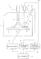
Fig. 1 is an explanatory drawing showing afilm deposition apparatus 1 and atemperature measuring apparatus 20 according to a first embodiment of the present invention,Fig. 2 shows details of a light emitting device, andFig. 3 shows details of a light detecting device. - In
Fig. 1 , thefilm deposition apparatus 1 for depositing a semiconductor layer by chemical vapor deposition (CVD) or molecular beam epitaxy (MBE) is illustrated in a schematic drawing. - The
film deposition apparatus 1 has achamber 2 that can be evacuated during deposition. A table 3 is disposed in thechamber 2, and aheater 3a is incorporated in the table 3 as a heating device. A feed port 4 is connected to thechamber 2, through which asource gas 5 containing elements (source molecules) for deposition of asemiconductor layer 7 is supplied to the surface of the table 3, thereby depositing thesemiconductor layer 7 on the surface of asubstrate 6 disposed on the table 3. - The
chamber 2 has a first window 8 and a second window 9. Transparent plates such as glass plate are inserted in the first window 8 and the second window 9 so that the inside can be observed through the transparent plate, but the interior space of thechamber 2 is separated from the exterior space by the transparent plate. - Outside the first window 8, a
pyrometer 10 is provided as an example of a temperature change measuring device. Thepyrometer 10 has alight receiver 11 and aprocessing circuit 12 which processes light output received by thelight receiver 11. Thelight receiver 11 of thepyrometer 10 is located outside the first window 8 at a normal angle to the surface of thesubstrate 6, looking through the transparent plate inserted in the first window 8. The axis of thelight receiver 11 lies on a perpendicular line Lv extending perpendicularly from the center of the surface of thesubstrate 6, and where a light receiving element inside thelight receiver 11 is facing the surface of thesubstrate 6 with its optical axis parallel to the perpendicular line Lv. - When the table 3 and the
substrate 6 are heated by theheater 3a, an infrared light emitted from the heated surface of the table 3 passes through thetransparent substrate 6 and thesemiconductor layer 7 during deposition and is received by thelight receiver 11 through the first window 8. The light output received by thelight receiver 11 is sent to theprocessing circuit 12, so that the surface temperature of thesubstrate 6, more precisely, the surface temperature of the table 3 can be determined from the wavelength of the received infrared light. - Outside the
chamber 2, alight emitting device 21 is provided as a constituent part of thetemperature measuring apparatus 20 according to the embodiment of the present invention. Thelight emitting device 21 is located outside the second window 9 of thechamber 2, facing the surface of thesubstrate 6. - As shown in
Fig. 2 , thelight emitting device 21 has a firstlaser beam source 22 which emits a laser beam L1 of a first wavelength and a secondlaser beam source 23 which emits a laser beam L2 of a second wavelength. The laser beam L1 emitted from the firstlaser beam source 22 is converted to a collimated light through acollimator lens 22a and then passes through ahalf mirror 25. The laser beam L2 emitted from the secondlight source 23 is converted to a collimated light through acollimator lens 23a and then reflected by amirror 24 to thehalf mirror 25. - In the
light emitting device 21, the firstlaser beam source 22 and the secondlaser beam source 23 are alternately turned on and off so that the first laser beam L1 and the second laser beam L2 can be alternately applied to thesubstrate 6 and thesemiconductor layer 7 along a common path Ld. - The
substrate 6 is made of a transparent materials such a sapphire wafer. In this context, "transparent" means having a total light transmittance of 80% or above as optical property, ideally, a total light transmittance of 95% or above. As shown inFig. 4 , abottom surface 6a of thesubstrate 6 is slightly rough, diffusing the reflected light at its surface. When the light transmission of thesemiconductor layer 7 is high, the laser beam irradiated along the path Ld can be diffusely reflected from thebottom surface 6a after passing through thesemiconductor layer 7 and thesubstrate 6. The diffuse reflected light R1 from thebottom surface 6a passes through thesubstrate 6 and thesemiconductor layer 7, and a component of the diffuse reflected light R1 directed along the perpendicular line Lv can be received by thelight receiver 11. - Since the laser beam travelling along the path Ld enters the
surface 7a of thesemiconductor layer 7 at an incidence angle θ, the light specularly reflected from thesurface 7a at the reflection angle θ cannot be received by thelight receiver 11. However, if the laser beam is diffusely reflected from thesurface 7a of thesemiconductor layer 7, a component part of the diffuse reflected light R2 directed along the perpendicular line Lv can be received by thelight receiver 11. - The angle θ which the path Ld makes with the perpendicular line Lv is greater than 0 degree and less than 90 degrees.
- The
light receiver 11 is not only used for thepyrometer 10 to receive an infrared light but also serves as a light detecting device which receives a laser light diffusely reflected from thebottom surface 6a and thesurface 7a. In thelight receiver 11, the infrared light emitted from theheated substrate 6 and thesemiconductor layer 7 and the diffuse reflected lights R1, R2 of the laser beam reflected from thesubstrate 6 and thesemiconductor layer 7 can be detected alternately in time. Moreover, light detection signals at thelight receiver 11 are divided in synchronization with the emission of the twolaser beam sources light receiver 11, the infrared light, the first laser beam L1 and the second laser beam L2 can be separately detected without interfering with each other. - Alternatively, a
light detecting device 16 which receives a laser beam may be provided separately from thelight receiver 11 of thepyrometer 10 which receives an infrared light, and thelight receiver 11 and the light detectingdevice 16 may be arranged side by side outside the first window 8. - In this case, as shown in
Fig. 3 , thelight detecting device 16 may be configured to include a firstlight receiving element 13, acondenser lens 13a for concentrating a reflected light to the firstlight receiving element 13, a secondlight receiving element 14, acondenser lens 14a for concentrating a reflected light to the secondlight receiving element 14, and awavelength filter 15. In the light detectingdevice 16, the diffuse reflected lights R1, R2 entering along the perpendicular line Lv can be split by thewavelength filter 15, so that the diffuse reflected light of the first laser beam L1 can be received by the firstlight receiving element 13 while the diffuse reflected light of the second laser beam can be received by the secondlight receiving element 14. - When using the
light detecting device 16 shown inFig. 3 , even if the firstlaser beam source 22 and the secondlaser beam sources 23 are simultaneously activated to continuously emit light in thelight emitting device 21 shown inFig. 2 , the diffuse reflected light of the first laser beam L1 and the diffuse reflected light of the second laser beam L2 can be separated from each other with thewavelength filter 15, so that the laser lights of different wavelengths can be separately received by the firstlight receiving element 13 and the secondlight receiving element 14. - As shown in
Fig. 1 , thefilm deposition apparatus 1, thepyrometer 10 and thelight emitting device 21 are controlled by acentral controller 30. Thecentral controller 30 comprises a microcomputer, a memory and so on. Aheating controller 31 receives an instruction from thecentral controller 30 and controls electric supply to theheater 3a, thereby controlling the heating temperature of the table 3. Alaser emission controller 32 receives an instruction from thecentral controller 30 and controls thelight emitting device 21. - An output signal of the
pyrometer 10 is sent to atemperature detecting device 33. Thetemperature detecting device 33 receives the output signal, which is correlated to the infrared light emitted from the table 3, determines the surface temperature of the table 3 from the wavelength of the infrared light or the like, and sends its temperature information to the central controller 30.In addition, the diffuse reflected light R1 of the laser beam diffusely reflected from thebottom surface 6a of thesubstrate 6 and the diffuse reflected light R2 of the laser beam diffusely reflected from thesurface 7a of thesemiconductor layer 7 are received by thelight receiver 11 or the light detectingdevice 16 shown inFig. 3 , and an output signal correlated to the amount of light detected is also sent to thetemperature detecting device 33, and its information is sent to thecentral controller 30. - Next will be described the principle of the method for measuring the temperature of the semiconductor layer using the measuring
apparatus 20. - In the
film deposition apparatus 1 shown inFig. 1 , thesource gas 5 is introduced into thechamber 2 while the table 3 and thesubstrate 6 are being heated by theheater 3a, whereby thesemiconductor layer 7 grows on the surface of thetransparent substrate 6, as shown inFig. 4 . - The
semiconductor layer 7 deposited on the surface of thesubstrate 6 serves as a monolayer in a light-emitting diode or other types of semiconductor elements and includes AlN, GaAs, GaN, InP, Si or SiC, for example. - In such semiconductor layers, the light transmittance varies depending on the wavelength of light and the temperature of the semiconductor layer. In
Fig. 5 , the abscissa represents the wavelength λ x of light applied to the semiconductor layer, while the ordinate represents the light transmittance in the semiconductor layer. InFig. 5 , the temperature of the same semiconductor layer is varied stepwise from T1 to T6 (T1 < T2 < T3 < T4 < T5 < T6). As shown inFig. 5 , when the light applied to the semiconductor layer has a given wavelength λ x, the light transmittance decreases with an increase in the temperature. In addition, as the temperature of the semiconductor layer increases, the temperature at which the transmittance starts to decrease varies depending on the wavelength λ x of the light applied to the semiconductor layer. - As a comparative example of the temperature measuring method according to the embodiment of the present invention,
Fig. 6 shows a temperature measuring method in which a single laser beam of a givenwavelength λ 1 is applied along the path Ld during deposition of thesemiconductor layer 7 onto the surface of thesubstrate 6 in thefilm deposition apparatus 1. InFig. 6 , the abscissa represents the temperature of thesemiconductor layer 7, while the ordinate represents the change in the detected light quantity when the diffusely reflected light of the laser beam from thebottom surface 6a of thesubstrate 6 and thesurface 7a of thesemiconductor layer 7 is received by thelight receiver 11. - As shown in
Fig. 6 , the changes in curve (i) represent a relationship between the change in the temperature of thesemiconductor layer 7 and the light quantity detected by thelight receiver 11 in an almost ideal condition without any diffuse reflected light R2 from thesurface 7a of thesemiconductor layer 7 or the like. - As indicated by the changes in curve (i), when the temperature of the
semiconductor layer 7 is low, thesemiconductor layer 7 has a high light transmission, so that the diffuse reflected light R1 reflected from thebottom surface 6a of thesubstrate 6 as shown inFig. 4 passes through thesemiconductor layer 7 at a high rate. Consequently, a large quantity of the diffuse reflected light of the laser beam can be received by thelight receiver 11, and the detected light quantity becomes D2. When the temperature of thesemiconductor layer 7 rises and reaches T1, the light transmittance of thesemiconductor layer 7 starts to decrease, so that the quantity of the diffuse reflected light received by thelight receiver 11 starts to decrease from D2. When the temperature of thesemiconductor layer 7 rises to T2, the light transmittance of thesemiconductor layer 7 becomes minimum, so that the detected quantity of the diffuse reflected light received by thelight receiver 11 decreases to D1. - In this description, a point (a) where the quantity of the diffuse reflected light detected by the
light receiver 11 starts to decrease with an increase in the temperature of thesemiconductor layer 7 is referred to as the "decrease starting point" and the detected light quantity D2 at the decrease starting point (a) is referred to as the "maximum detected light quantity". On the other hand, a point (b) where the decrease in the quantity of the diffuse reflected light detected by thelight receiver 11 ends is referred to as the "decrease ending point" and the detected light quantity D1 at the decrease ending point (b) is referred to as the "minimum detected light quantity". - In an actual film deposition process of the
semiconductor layer 7, the optical properties of thesubstrate 6 and thesemiconductor layer 7 easily vary depending on temperature conditions as well as the direction and roughness of thesurface 7a of thesemiconductor layer 7 easily vary. In addition, when thesubstrate 6 is placed in thechamber 2, an error easily arises in the angle between thesurface 6a of thesubstrate 6 and the perpendicular line Lv. As the properties of diffused reflection of the laser beam vary with these various conditions, even if the light transmittance of thesame semiconductor layer 7 is measured by using the same laser beam ofwavelength λ 1, the change in the light quantity detected by thelight receiver 11 cannot follow the ideal curve (i) shown inFig. 6 , but will include the offsetquantities δ 1 andδ 2, as shown by the dotted curve (ii). - However, even if the conditions for diffused reflection of the laser beam from the
substrate 6 or thesemiconductor layer 7 vary, the relationship between the wavelength and the transmittance of light and the relationship with the current temperature remain the same as long as a laser beam of the same wavelength is irradiated on a semiconductor layer of the same material, as shown inFig. 5 . Accordingly, the temperature of thesemiconductor layer 7 is T1 not only at the decrease starting point (a) of the curve (i) but also at a decrease starting point (c) of the curve (ii), and the temperature of thesemiconductor layer 7 is T2 not only at the decrease ending point (b) of the curve (i) but also at a decrease ending point (d) of the curve (ii). - In other words, although the light transmittance of the
semiconductor layer 7 does not vary as long as the temperature and the wavelength remain the same, the quantity of the diffused reflected light of the laser beam detected by thelight receiver 11 varies according to various optical conditions other than the transmittance such as diffused reflection conditions. - In the temperature measuring method using a single laser beam of a
wavelength λ 1, if the curve shown inFig. 6 is obtained by increasing the temperature of thesemiconductor layer 7 during deposition to a value higher than the temperature T2 corresponding to the decrease ending point, as shown inFig. 6 , then, the temperature of thesemiconductor layer 7 between T1 and T2 can be calculated by monitoring a detected light quantity Da. Once a relationship between the maximum value D2, the minimum value D1 and the temperatures T2, T1 in the variation of the curve (i) is found by raising the temperature of thesemiconductor layer 7 above T2, for example, the current temperature Tx of thesemiconductor layer 7 can be calculated from the monitored value Da of the detected light quantity according to the following equation:
- However, if the temperature is not raised to T2 or the relationship between (T2 - T1) and (D2 - D1) is unknown, the temperature Tx between T2 and T1 cannot be calculated from the monitored value of the temperature during deposition, so that it is impossible to perform the control to keep the temperature of the
semiconductor layer 7 at Tx. - In the method for measuring the temperature of the semiconductor layer using the measuring
apparatus 20 according to the embodiment of the present invention, however, since at least two types of laser beams having different wavelengths are used, the temperature Tx between T2 and T1 can be calculated from the monitored value of the light quantity of the laser beam detected by thelight receiver 11 without raising the temperature of thesemiconductor layer 7 above T2. - In the
film deposition apparatus 1 shown inFig. 1 , the first laser beam L1 is emitted from the firstlaser beam source 22 of thelight emitting device 21 shown inFig. 2 , while the second laser beam L2 is emitted from the secondlight source 23, and these laser beams L1, L2 are applied to thesemiconductor layer 7 along the same path Ld. - A curve (iii) shown in
Fig. 7 represents a relationship between the detected light quantity and the temperature of thesemiconductor layer 7 when the first laser beam L1 is applied to thesemiconductor layer 7 placed on thesubstrate 6 and the diffuse reflected lights R1, R2 are received by thelight receiver 11, while a curve (iv) represents a relationship between the detected light quantity and the temperature of thesemiconductor layer 7 when the second laser beam L2 is applied to thesemiconductor layer 7 placed on thesubstrate 6 and the diffuse reflected lights R1, R2 are received by thelight receiver 11. - The wavelength of the first laser beam L1 is selected such that the temperature of the
semiconductor layer 7 is T3 at a decrease starting point (e) and T4 at a decrease ending point (f). The wavelength of the second laser beam L2 is selected such that the temperature is T5 at a decrease starting point (g) and T6 at a decrease ending point (h). The range from the temperature T3 to T4 is a first temperature range in which the light transmission quantity of the first laser beam L1 decreases, while the range from the temperature T5 to T6 is a second temperature range in which the light transmission quantity of the second laser beam L2 decreases. The second temperature range is higher than the first temperature range. - As shown in
Fig. 5 , depending on the type of material, thesemiconductor layer 7 has a certain relationship between the transmittance and the wavelength for each temperature, so that the first temperature range can be set by selecting the wavelength of the first laser beam L1 depending on the material of thesemiconductor layer 7, and in the same fashion the second temperature range can be set by selecting the wavelength of the second laser beam L2 depending on the material. - Since the first laser beam L1 and the second laser beam L2 are applied to the
semiconductor layer 7 along the same path Ld, the first laser beam L1 and the second laser beam L2 are equally subjected to the influence of transmission and reflection properties of light, e.g., the influence of the diffused reflection from thebottom surface 6a of thesubstrate 6, the influence of the surface roughness at thesurface 7 of thesemiconductor layer 7, and the error in the angle between thesurface 7a of thesemiconductor layer 7 and the perpendicular line Lv. Consequently, the ratio of thechanges δ 1,δ 2 in the detected light quantity shown inFig. 6 does not vary between the first laser beam L1 and the second laser beam L2. - Therefore, if the
light emitting device 21 has the same emission intensity for both the first laser beam L1 and the second laser beam L2 and thelight receiver 11 has the same photosensitivity for both the first laser beam L1 and the second laser beam L2, both maximum of detected light quantity associated with the first laser beam L1 and the second laser beam L2 become D4, as shown inFig. 7 , and in the same way, the decrease of light quantity of the first laser beam L1 and the decrease of light quantity of the second laser beam L2 are equal and become (D4 - D3). - In practice, however, since the emission intensity differs between the two laser beams and the light reception sensitivity also differs between these laser beams, it is necessary to perform some calibrations before performing the film deposition in the
apparatus 1. - An example of calibration is such that the
substrate 6, on which a sample of the semiconductor layer has been previously deposited, is placed on the table 3 in thechamber 2, and where the temperature of thesubstrate 6, as well as that of thesemiconductor layer 7 is gradually increased under monitoring with thepyrometer 10, while the first laser beam L1 and the second laser beam L2 are applied to the sample of the semiconductor layer. A change in the detected light quantity of the first laser beam L1 is measured as the temperature exceeds the first temperature range (T3-T4), and a change in the detected light quantity of the second laser beam L2 is measured as the temperature exceeds the second temperature range (T5-T6). Based on these measured values, software or hardware adjustments are performed such that a decrease in the detected light quantity of the first laser beam L1 in the first temperature range becomes equal to a decrease in the detected light quantity of the second laser beam L2 in the second temperature range. - Another example of calibration is as follows. In the case where the
semiconductor layer 7 has not been deposited on thetransparent substrate 6 in thechamber 2, the laser beam is emitted from the firstlaser beam source 22 shown inFig.2 and the diffused reflection of the first laser beam L1 from thebottom surface 6a of thesubstrate 6 and from the surface of thesubstrate 6 is detected by thelight receiver 11. Then, the laser beam is emitted from the secondlaser beam source 23 and the diffused reflection of the second laser beam L2 from thebottom surface 6a of thesubstrate 6 and from the surface of thesubstrate 6 is detected by thelight receiver 11. Finally, the calibration is performed by software or hardware adjustments such that the light quantity detected when the laser beam is emitted from the firstlaser beam source 22 becomes equal to the light quantity detected when the laser beam is emitted from the secondlaser beam source 23. - In the
film deposition apparatus 1 thus calibrated, the temperature Ty in the second temperature range between the temperatures T5 and T6 can be immediately calculated from the monitored value of the light quantity of the laser beam detected by thelight receiver 11, where the temperature of thesemiconductor layer 7 need not be raised above T6 shown inFig. 7 . - As shown in
Fig. 7 , as the temperature of thesemiconductor layer 7 rises, the detected light quantity of the first laser beam L1 passes through the decrease starting point (e) and reaches the decrease ending point (f), as indicated by the curve (iii). At this point, the detected light quantity of the second laser beam L2 has not yet started to decrease, as shown by the curve (iv). When the detected light quantity of the first laser beam L1 has passed through the decrease ending point (f), the decrease (D4 - D3) in the detected light quantity of the first laser beam L1 can be determined by theprocessing circuit 12 of thelight receiver 11 and sent to thecentral controller 30 for storage through thetemperature detecting device 33. - Thereafter, as the temperature of the
semiconductor layer 7 rises, the detected light quantity of the second laser beam L2 reaches the decrease starting point (g) and starts to decrease. At this time, since the decrease (D4 - D3) in the detected light quantity of the first laser beam L1 has been already found, the temperature Ty of thesemiconductor layer 7 can be calculated by thecentral controller 30 from a monitored value Db that is obtained when the detected light quantity of the second laser beam L2 has passed through the decrease starting point (g) but not yet reached the decrease ending point (h) and the decrease (D4 - D3) in the first laser beam L1 according to the following equation:
- That is, the current temperature of the
semiconductor layer 7 can be calculated such that (the maximum temperature of the second range) + (the temperature difference of the second range) × {(the decrease in the transmission quantity of the second wavelength light from the decrease starting point to the current point)/(the decrease in the detected quantity of the first wavelength light)}. - Accordingly, as the temperature of the
semiconductor layer 7 rises, the temperature of thesemiconductor layer 7 can be controlled to be the temperature Ty between the temperatures T5 and T6 by monitoring the temperature after the second laser beam L2 has passed through the decrease starting point (g). - The relationship between the light transmittance and the current temperature in the case where the second laser beam L2 is irradiated on the
semiconductor layer 7 can be established depending on the relationship between the material of the semiconductor and the wavelength of the laser beam L2. When thesemiconductor layer 7 is made of GaN (gallium nitride) and the wavelength of the second laser beam L2 is 445 nm, for example, the temperature T5 at the decrease starting point (g) can be set at about 800°C and the temperature T6 at the decrease ending point (h) can be set at about 900°C. In this case, the temperature at which occurs the deposition of thesemiconductor layer 7 can always be controlled to be a certain temperature between 800°C and 900°C. - It should be noted that the wavelength of the first laser beam L1 can be selected from a relatively wide range as long as the temperature T4 at the decrease ending point (f) is lower than the temperature T5 at the decrease starting point (g) of the second laser beam L2.
- In the
film deposition apparatus 1 shown inFig. 1 , the temperature of thesemiconductor layer 7 is indirectly measured such that the infrared light emitted from thesubstrate 6 and the surface of thesemiconductor layer 7 is detected by thepyrometer 10, which is an example of the temperature change measuring device, and an output signal correlated to the infrared light is sent to thetemperature detecting device 33. The temperature information acquired by the detection of the infrared light at thepyrometer 10 can be corrected by comparing the temperature information with the temperature calculated by using the first laser beam L1 and the second laser beam L2. It is also possible to perform the temperature control with higher accuracy based on the temperature calculated by using the first laser beam L1 and the second laser beam L2 and the temperature information acquired by the detection of the infrared light. -
Fig. 8 shows a temperature control method for controlling the temperature of thesemiconductor layer 7 to be a certain temperature Ty within the second temperature range (T6 - T5) during deposition of thesemiconductor layer 7 in thechamber 1. - In
Fig. 8 , a dotted line T represents a change in the temperature of thesemiconductor layer 7 during deposition onto thesubstrate 6. A curve (v) represents a change in the light quantity of the first laser beam L1 detected by thelight receiver 11, while a curve (vi) represents a change in the light quantity of the second laser beam L2 detected by thelight receiver 11. - When the
semiconductor layer 7 is being deposited with thesource gas 5 introduced into thechamber 2, theheater 3a is controlled to raise the temperature T of thesemiconductor layer 7. The detected light quantity of the first laser beam L1 reaches a decrease starting point (k) at a time τ a and then reaches a decrease ending point (m), and thus, a decrease (D6 - D5) of the first laser beam L1 can be determined when the temperature of thesemiconductor layer 7 exceeds the first temperature range. - Once the detected light quantity of the second laser beam L2 passes through a decrease starting point (n) along with a further rise in the temperature of the
substrate 6 and thesemiconductor layer 7, it becomes possible to immediately calculate the actual temperature of thesemiconductor layer 7 from the monitored value of the received light quantity of the second laser beam L2 by thelight receiver 11 and the previously determined decrease (D6 - D5) of the first laser beam L1. Accordingly, once the detected light quantity of the second laser beam L2 reaches Dc between D6 and D5 at a time τ b, the temperature of thesemiconductor layer 7 can be maintained at an optimum temperature Ty for deposition in the second temperature range (T5 - T6) by controlling theheater 3a with theheating controller 31 and keeping the monitored value of the detected light quantity at Dc. - As shown in
Fig. 8 , once the decrease (D6 - D5) in the detected light quantity of the first laser beam L1 is determined, the temperature of thesemiconductor layer 7 can be maintained at the optimum temperature Ty for deposition by monitoring the detected light quantity of the second laser beam L2 without the need to raise the temperature of thesemiconductor layer 7 above the second temperature range. -
Figs. 9 and10 show a case where although the temperature of thesemiconductor layer 7 is being controlled to be the optimum value Ty after the time τ b, a change has occurred in the light quantity detected by thelight receiving element 11. - In the case shown in
Fig. 9 , the detected light quantity of the second laser beam L2 does not stay at Dc and varies as indicated by α during the temperature control after the time τ b. At the same time, the detected light quantity of the first laser beam L1 does not stay at the minimum value D5, either, and has a change β similar to α. When the detected light quantity of the first laser beam L1 and the detected light quantity of the second laser beam L2 vary in a similar manner, as described above, it can be determined that a change has occurred in the laser beam incidence reflection conditions of thesemiconductor layer 7, e.g., that a change has occurred in the diffuse reflected light R2 because of a change in the surface roughness at thesurface 7a of thesemiconductor layer 7. - On the other hand, if the detected light quantity of the second laser beam L2 has a change α but the detected light quantity of the first laser beam L1 does not show any changes after the decrease ending point (m), as shown in
Fig. 10 , it can be determined that this change is not due to a variation of the light transmission conditions or reflection conditions for the two laser beams of different wavelengths, but due to a real change of temperature Tz at thesemiconductor layer 7. - That is, once the detected light quantity of the first laser beam L1 passes through the decrease ending point (m), it becomes possible to determine whether a change has occurred in the temperature of the
semiconductor layer 7 or an optical change has occurred in thesemiconductor layer 7 by monitoring both the detected light quantity of the first laser beam L1 and the detected light quantity of the second laser beam L2. - For instance, the diffuse reflected light R2 from the
surface 7a may increase because of surface roughness caused by partial evaporation of thesurface 7a during the deposition of thesemiconductor layer 7, but this phenomenon can be detected by the foregoing monitoring, and the occurrence of surface roughness at thesurface 7a can be suppressed by controlling the introduction amount of thesource gas 5 and the heating temperature. It is also possible to purposely impart surface roughness to thesurface 7a of thesemiconductor layer 7 by controlling them. - In addition, if a relationship between at least one of a change α in the detected light quantity of the first laser beam L1 or a change β in the detected light quantity of the second laser beam L2 and the degree of surface roughness or an acceptable range of surface roughness at the
surface 7a of thesemiconductor layer 7 has been previously found and its function is stored in thecentral controller 30, the surface roughness at thesurface 7a of thesemiconductor layer 7 can be calculated when the changes α, β appear in the detected light quantity, as shown inFig. 9 . For example, the degree of surface roughness at thesurface 7a of thesemiconductor layer 7 can be determined from a ratio of the maximum value D6 of the detected light quantity to the magnitude of the changes α, β or a ratio of the change (D6 - D5) in the detected light quantity to the magnitude of the changes α, β. With this, the degree of actual surface roughness can be estimated numerically or used for relatively rough determination of whether the surface roughness is within an acceptable range or not. - In the temperature measuring apparatus and method according to the present invention, it is also possible that the light detecting
device 10 is opposed to the surface of thesubstrate 6 in the same manner as inFig. 1 , whereas thelight emitting device 21 which emits the laser beams L1, L2 of different wavelengths is opposed to the bottom surface of thesubstrate 6. In this case, after having entered thebottom surface 6a of thesubstrate 6 and passed through thesubstrate 6 and thesemiconductor layer 7, the first laser beam L1 and the second laser beam L2 can be received by thelight receiver 11. - Also in this case, the temperature of the
semiconductor layer 7 can be measured as needed despite any optical changes other than a change in the light transmittance of the semiconductor layer such as the surface roughness at the surface of thesemiconductor layer 7, which are canceled by using the laser beams L1 and L2 of different wavelengths, as in the first embodiment. -
- 1
- Film Deposition Apparatus
- 2
- Chamber
- 3
- Table
- 6
- Substrate
- 7
- Semiconductor Layer
- 8
- First Window
- 9
- Second Window
- 10
- Pyrometer
- 11
- Light Receiver
- 13
- First Light Receiving Element
- 14
- Second Light Receiving Element
- 15
- Wavelength Filter
- 16
- Light Detecting Device
- 20
- Temperature Measuring Apparatus
- 21
- Light Emitting Device
- 22
- First Laser Beam Source
- 23
- Second Laser Beam Source
- L1
- Laser Beam of First Wavelength
- L2
- Laser Beam of Second Wavelength
- T3-T4
- First Temperature Range
- T5-T6
- Second Temperature Range
- (e), (g)
- Decrease Starting Point
- (f), (h)
- Decrease Ending Point
Claims (5)
- A method for measuring a temperature of a semiconductor layer (7) during deposition in a chamber (2), comprising
applying monochromatic light from a laser at a first wavelength (L1) and monochromatic light from a laser at a second wavelength (L2) to the semiconductor layer (7) along a common optical path and detecting quantities of the first wavelength light (L1) and the second wavelength light (L2) coming from the semiconductor layer (7) with a light detecting device (16) facing the semiconductor layer (7),
the first wavelength (L1) being selected such that the transmittance of the semiconductor layer (7) decreases from start to end of a first increasing temperature range (T3-T4) of the semiconductor layer (7) but does not change from start to end of a second increasing temperature range (T5-T6) of the semiconductor layer (7), the temperature of the semiconductor layer (7) being higher at the start of the second increasing temperature range (T5-T6) than at the end of the first increasing temperature range (T3-T4),
the second wavelength (L2) being selected such that the transmittance of the semiconductor layer (7) does not change from start to end of the first increasing temperature range (T3-T4) but decreases from start to end of the second increasing temperature range (T5-T6),
wherein when a change in the detected quantity of the second wavelength (L2) is observed in the second increasing temperature range (T5-T6) without any change in the detected quantity of the first wavelength (L1), it is determined that the change is due to a change in the temperature of the semiconductor layer (7),
when a change in the detected quantity is observed in both the first wavelength (L1) and the second wavelength (L2), it is determined that the change is due to a factor other than a change in the temperature of the semiconductor layer (7). - The method of Claim 1, wherein a temperature (Ty) of the semiconductor layer (7) is determined from a detected light quantity (Db) of the second wavelength (L2), the detected light quantity (D4) of the first wavelength (L1) at the start of the first increasing temperature range (T3-T4) and the detected light quantity (D3) of the first wavelength (L1) at the end of the first increasing temperature range (T3-T4).
- The method of Claim 1 or 2, wherein a change in the detected light quantity observed in both the first wavelength (L1) and the second wavelength (L2) is attributed to a change of the semiconductor layer (7) surface roughness.
- The method of Claim 3, wherein based on a previously determined relationship between at least one of either the change in the detected light quantity of the first wavelength (L1) or the change in the detected light quantity of the second wavelength (L2) and the surface roughness of the semiconductor layer (7), the surface roughness of the semiconductor layer (7) is quantified using at least one of either the change in the detected light quantity of the first wavelength (L1) or the change in the detected light quantity of the second wavelength (L2).
- A method for measuring a temperature of a semiconductor layer according to any one of Claims 1 to 4, wherein the temperature of the semiconductor layer is also measured by detecting an infrared light emitted from the semiconductor layer with a temperature change measuring device, and a measurement error of the temperature change measuring device is corrected based on the calculated current temperature within the second range.
Applications Claiming Priority (1)
| Application Number | Priority Date | Filing Date | Title |
|---|---|---|---|
| PCT/JP2011/067678 WO2013018197A1 (en) | 2011-08-02 | 2011-08-02 | Method and apparatus for measuring temperature of semiconductor layer |
Publications (3)
| Publication Number | Publication Date |
|---|---|
| EP2741062A1 EP2741062A1 (en) | 2014-06-11 |
| EP2741062A4 EP2741062A4 (en) | 2014-12-10 |
| EP2741062B1 true EP2741062B1 (en) | 2017-02-01 |
Family
ID=47628760
Family Applications (1)
| Application Number | Title | Priority Date | Filing Date |
|---|---|---|---|
| EP11870369.3A Active EP2741062B1 (en) | 2011-08-02 | 2011-08-02 | Method for measuring temperature of semiconductor layer |
Country Status (8)
| Country | Link |
|---|---|
| US (1) | US9823132B2 (en) |
| EP (1) | EP2741062B1 (en) |
| JP (1) | JP5725584B2 (en) |
| KR (1) | KR101834034B1 (en) |
| CN (1) | CN103649702B (en) |
| CA (1) | CA2837164C (en) |
| TW (1) | TWI557399B (en) |
| WO (1) | WO2013018197A1 (en) |
Families Citing this family (6)
| Publication number | Priority date | Publication date | Assignee | Title |
|---|---|---|---|---|
| US10845249B2 (en) | 2017-05-26 | 2020-11-24 | Applied Materials, Inc. | Continuous spectra transmission pyrometry |
| US10571337B2 (en) | 2017-05-26 | 2020-02-25 | Applied Materials, Inc. | Thermal cooling member with low temperature control |
| US10281335B2 (en) | 2017-05-26 | 2019-05-07 | Applied Materials, Inc. | Pulsed radiation sources for transmission pyrometry |
| SG10201705708YA (en) | 2017-05-26 | 2018-12-28 | Applied Materials Inc | Detector for low temperature transmission pyrometry |
| CN109443589A (en) * | 2018-08-29 | 2019-03-08 | 宁波中车时代传感技术有限公司 | A kind of temperature monitoring system of IGBT module and IGBT module |
| JP7362505B2 (en) * | 2020-02-20 | 2023-10-17 | 東京エレクトロン株式会社 | Substrate liquid processing device and liquid discharge evaluation method |
Family Cites Families (16)
| Publication number | Priority date | Publication date | Assignee | Title |
|---|---|---|---|---|
| US5229303A (en) * | 1989-08-29 | 1993-07-20 | At&T Bell Laboratories | Device processing involving an optical interferometric thermometry using the change in refractive index to measure semiconductor wafer temperature |
| GB2238868A (en) | 1989-11-22 | 1991-06-12 | Res Corp Technologies Inc | Silicon wafer temperature measurement by optical transmission monitoring. |
| US5474381A (en) * | 1993-11-30 | 1995-12-12 | Texas Instruments Incorporated | Method for real-time semiconductor wafer temperature measurement based on a surface roughness characteristic of the wafer |
| US5835225A (en) * | 1994-11-30 | 1998-11-10 | Micron Technology, Inc. | Surface properties detection by reflectance metrology |
| US5618461A (en) | 1994-11-30 | 1997-04-08 | Micron Technology, Inc. | Reflectance method for accurate process calibration in semiconductor wafer heat treatment |
| JP3366538B2 (en) | 1996-11-29 | 2003-01-14 | 大日本スクリーン製造株式会社 | Temperature measuring apparatus and substrate heat treatment apparatus using the same |
| US6116779A (en) * | 1997-03-10 | 2000-09-12 | Johnson; Shane R. | Method for determining the temperature of semiconductor substrates from bandgap spectra |
| WO2001050109A2 (en) * | 2000-01-05 | 2001-07-12 | Tokyo Electron Limited | Wafer band-edge measurement using spectroscopy and a process of uniform wafer temperature control |
| JP2001289714A (en) | 2000-04-07 | 2001-10-19 | Matsushita Electric Ind Co Ltd | Temperature measurement method and measurement device of substrate and treating device of the substrate |
| JP2002122480A (en) | 2000-10-12 | 2002-04-26 | Toshiba Corp | Method and device for measuring temperature, and plasma treatment device |
| JP2002367907A (en) | 2001-06-04 | 2002-12-20 | Inst Of Physical & Chemical Res | Crystal growth apparatus and method therefor |
| US20050106876A1 (en) * | 2003-10-09 | 2005-05-19 | Taylor Charles A.Ii | Apparatus and method for real time measurement of substrate temperatures for use in semiconductor growth and wafer processing |
| JP5076278B2 (en) * | 2005-03-14 | 2012-11-21 | 日亜化学工業株式会社 | Field effect transistor |
| US7543981B2 (en) * | 2006-06-29 | 2009-06-09 | Mattson Technology, Inc. | Methods for determining wafer temperature |
| US8283607B2 (en) * | 2008-04-09 | 2012-10-09 | Applied Materials, Inc. | Apparatus including heating source reflective filter for pyrometry |
| KR101532468B1 (en) * | 2008-12-26 | 2015-06-29 | 유우겐가이샤 와이시스템즈 | Method and device for measuring temperature during deposition of semiconductor |
-
2011
- 2011-08-02 JP JP2013526678A patent/JP5725584B2/en active Active
- 2011-08-02 CA CA2837164A patent/CA2837164C/en active Active
- 2011-08-02 US US14/126,010 patent/US9823132B2/en active Active
- 2011-08-02 CN CN201180071888.2A patent/CN103649702B/en active Active
- 2011-08-02 WO PCT/JP2011/067678 patent/WO2013018197A1/en active Application Filing
- 2011-08-02 EP EP11870369.3A patent/EP2741062B1/en active Active
- 2011-08-02 KR KR1020137034382A patent/KR101834034B1/en active IP Right Grant
-
2012
- 2012-07-23 TW TW101126472A patent/TWI557399B/en active
Non-Patent Citations (1)
| Title |
|---|
| None * |
Also Published As
| Publication number | Publication date |
|---|---|
| CN103649702B (en) | 2016-08-17 |
| CA2837164A1 (en) | 2013-02-07 |
| CN103649702A (en) | 2014-03-19 |
| KR20140040763A (en) | 2014-04-03 |
| US20140192839A1 (en) | 2014-07-10 |
| CA2837164C (en) | 2017-08-22 |
| KR101834034B1 (en) | 2018-03-02 |
| EP2741062A1 (en) | 2014-06-11 |
| WO2013018197A1 (en) | 2013-02-07 |
| EP2741062A4 (en) | 2014-12-10 |
| US9823132B2 (en) | 2017-11-21 |
| JPWO2013018197A1 (en) | 2015-03-02 |
| TW201321730A (en) | 2013-06-01 |
| TWI557399B (en) | 2016-11-11 |
| JP5725584B2 (en) | 2015-05-27 |
Similar Documents
| Publication | Publication Date | Title |
|---|---|---|
| EP2741062B1 (en) | Method for measuring temperature of semiconductor layer | |
| US9453721B2 (en) | Curvature measurement apparatus and method | |
| US5564830A (en) | Method and arrangement for determining the layer-thickness and the substrate temperature during coating | |
| US8673656B2 (en) | Method and device for measuring temperature during deposition of semiconductor | |
| US8786841B2 (en) | Thin film temperature measurement using optical absorption edge wavelength | |
| KR20050014877A (en) | System and process for calibrating temperature measurement devices in thermal processing chambers | |
| US9443715B2 (en) | Method and device for measuring temperature of substrate in vacuum processing apparatus | |
| US20180223434A1 (en) | Vapor growth apparatus, and vapor growth method | |
| US20110212256A1 (en) | Deposition rate control | |
| US20230374664A1 (en) | Method for emissivity-corrected pyrometry | |
| US9885612B2 (en) | Optical temperature sensor and method of controlling same | |
| US6283630B1 (en) | Temperature measuring method using radiation thermometer | |
| US20030231694A1 (en) | Temperature-measuring device | |
| US20210233787A1 (en) | Warp measurement device, vapor deposition apparatus, and warp measurement method | |
| JP2018166204A (en) | Film forming apparatus and film forming method | |
| US20210381899A1 (en) | Method and device for the in-situ determination of the temperature of a sample | |
| JPH1062129A (en) | Film thickness measuring method | |
| US20030205199A1 (en) | Method and apparatus for non-contact, in-situ temperature measurement of a substrate film during chemical vapor deposition of the substrate film |
Legal Events
| Date | Code | Title | Description |
|---|---|---|---|
| PUAI | Public reference made under article 153(3) epc to a published international application that has entered the european phase |
Free format text: ORIGINAL CODE: 0009012 |
|
| 17P | Request for examination filed |
Effective date: 20131120 |
|
| AK | Designated contracting states |
Kind code of ref document: A1 Designated state(s): AL AT BE BG CH CY CZ DE DK EE ES FI FR GB GR HR HU IE IS IT LI LT LU LV MC MK MT NL NO PL PT RO RS SE SI SK SM TR |
|
| DAX | Request for extension of the european patent (deleted) | ||
| A4 | Supplementary search report drawn up and despatched |
Effective date: 20141110 |
|
| RIC1 | Information provided on ipc code assigned before grant |
Ipc: C30B 25/16 20060101ALI20141104BHEP Ipc: C30B 25/02 20060101ALI20141104BHEP Ipc: G01K 11/12 20060101AFI20141104BHEP Ipc: C23C 16/52 20060101ALI20141104BHEP Ipc: H01L 21/205 20060101ALI20141104BHEP |
|
| 17Q | First examination report despatched |
Effective date: 20160401 |
|
| GRAP | Despatch of communication of intention to grant a patent |
Free format text: ORIGINAL CODE: EPIDOSNIGR1 |
|
| INTG | Intention to grant announced |
Effective date: 20160908 |
|
| GRAS | Grant fee paid |
Free format text: ORIGINAL CODE: EPIDOSNIGR3 |
|
| GRAA | (expected) grant |
Free format text: ORIGINAL CODE: 0009210 |
|
| AK | Designated contracting states |
Kind code of ref document: B1 Designated state(s): AL AT BE BG CH CY CZ DE DK EE ES FI FR GB GR HR HU IE IS IT LI LT LU LV MC MK MT NL NO PL PT RO RS SE SI SK SM TR |
|
| REG | Reference to a national code |
Ref country code: GB Ref legal event code: FG4D |
|
| REG | Reference to a national code |
Ref country code: CH Ref legal event code: EP Ref country code: AT Ref legal event code: REF Ref document number: 865979 Country of ref document: AT Kind code of ref document: T Effective date: 20170215 |
|
| REG | Reference to a national code |
Ref country code: IE Ref legal event code: FG4D |
|
| REG | Reference to a national code |
Ref country code: DE Ref legal event code: R096 Ref document number: 602011034858 Country of ref document: DE |
|
| REG | Reference to a national code |
Ref country code: NL Ref legal event code: MP Effective date: 20170201 |
|
| REG | Reference to a national code |
Ref country code: LT Ref legal event code: MG4D |
|
| REG | Reference to a national code |
Ref country code: AT Ref legal event code: MK05 Ref document number: 865979 Country of ref document: AT Kind code of ref document: T Effective date: 20170201 |
|
| PG25 | Lapsed in a contracting state [announced via postgrant information from national office to epo] |
Ref country code: HR Free format text: LAPSE BECAUSE OF FAILURE TO SUBMIT A TRANSLATION OF THE DESCRIPTION OR TO PAY THE FEE WITHIN THE PRESCRIBED TIME-LIMIT Effective date: 20170201 Ref country code: IS Free format text: LAPSE BECAUSE OF FAILURE TO SUBMIT A TRANSLATION OF THE DESCRIPTION OR TO PAY THE FEE WITHIN THE PRESCRIBED TIME-LIMIT Effective date: 20170601 Ref country code: NO Free format text: LAPSE BECAUSE OF FAILURE TO SUBMIT A TRANSLATION OF THE DESCRIPTION OR TO PAY THE FEE WITHIN THE PRESCRIBED TIME-LIMIT Effective date: 20170501 Ref country code: GR Free format text: LAPSE BECAUSE OF FAILURE TO SUBMIT A TRANSLATION OF THE DESCRIPTION OR TO PAY THE FEE WITHIN THE PRESCRIBED TIME-LIMIT Effective date: 20170502 Ref country code: FI Free format text: LAPSE BECAUSE OF FAILURE TO SUBMIT A TRANSLATION OF THE DESCRIPTION OR TO PAY THE FEE WITHIN THE PRESCRIBED TIME-LIMIT Effective date: 20170201 Ref country code: LT Free format text: LAPSE BECAUSE OF FAILURE TO SUBMIT A TRANSLATION OF THE DESCRIPTION OR TO PAY THE FEE WITHIN THE PRESCRIBED TIME-LIMIT Effective date: 20170201 |
|
| PG25 | Lapsed in a contracting state [announced via postgrant information from national office to epo] |
Ref country code: PL Free format text: LAPSE BECAUSE OF FAILURE TO SUBMIT A TRANSLATION OF THE DESCRIPTION OR TO PAY THE FEE WITHIN THE PRESCRIBED TIME-LIMIT Effective date: 20170201 Ref country code: RS Free format text: LAPSE BECAUSE OF FAILURE TO SUBMIT A TRANSLATION OF THE DESCRIPTION OR TO PAY THE FEE WITHIN THE PRESCRIBED TIME-LIMIT Effective date: 20170201 Ref country code: SE Free format text: LAPSE BECAUSE OF FAILURE TO SUBMIT A TRANSLATION OF THE DESCRIPTION OR TO PAY THE FEE WITHIN THE PRESCRIBED TIME-LIMIT Effective date: 20170201 Ref country code: BG Free format text: LAPSE BECAUSE OF FAILURE TO SUBMIT A TRANSLATION OF THE DESCRIPTION OR TO PAY THE FEE WITHIN THE PRESCRIBED TIME-LIMIT Effective date: 20170501 Ref country code: AT Free format text: LAPSE BECAUSE OF FAILURE TO SUBMIT A TRANSLATION OF THE DESCRIPTION OR TO PAY THE FEE WITHIN THE PRESCRIBED TIME-LIMIT Effective date: 20170201 Ref country code: PT Free format text: LAPSE BECAUSE OF FAILURE TO SUBMIT A TRANSLATION OF THE DESCRIPTION OR TO PAY THE FEE WITHIN THE PRESCRIBED TIME-LIMIT Effective date: 20170601 Ref country code: NL Free format text: LAPSE BECAUSE OF FAILURE TO SUBMIT A TRANSLATION OF THE DESCRIPTION OR TO PAY THE FEE WITHIN THE PRESCRIBED TIME-LIMIT Effective date: 20170201 Ref country code: LV Free format text: LAPSE BECAUSE OF FAILURE TO SUBMIT A TRANSLATION OF THE DESCRIPTION OR TO PAY THE FEE WITHIN THE PRESCRIBED TIME-LIMIT Effective date: 20170201 Ref country code: ES Free format text: LAPSE BECAUSE OF FAILURE TO SUBMIT A TRANSLATION OF THE DESCRIPTION OR TO PAY THE FEE WITHIN THE PRESCRIBED TIME-LIMIT Effective date: 20170201 |
|
| PG25 | Lapsed in a contracting state [announced via postgrant information from national office to epo] |
Ref country code: EE Free format text: LAPSE BECAUSE OF FAILURE TO SUBMIT A TRANSLATION OF THE DESCRIPTION OR TO PAY THE FEE WITHIN THE PRESCRIBED TIME-LIMIT Effective date: 20170201 Ref country code: SK Free format text: LAPSE BECAUSE OF FAILURE TO SUBMIT A TRANSLATION OF THE DESCRIPTION OR TO PAY THE FEE WITHIN THE PRESCRIBED TIME-LIMIT Effective date: 20170201 Ref country code: IT Free format text: LAPSE BECAUSE OF FAILURE TO SUBMIT A TRANSLATION OF THE DESCRIPTION OR TO PAY THE FEE WITHIN THE PRESCRIBED TIME-LIMIT Effective date: 20170201 Ref country code: CZ Free format text: LAPSE BECAUSE OF FAILURE TO SUBMIT A TRANSLATION OF THE DESCRIPTION OR TO PAY THE FEE WITHIN THE PRESCRIBED TIME-LIMIT Effective date: 20170201 Ref country code: RO Free format text: LAPSE BECAUSE OF FAILURE TO SUBMIT A TRANSLATION OF THE DESCRIPTION OR TO PAY THE FEE WITHIN THE PRESCRIBED TIME-LIMIT Effective date: 20170201 |
|
| REG | Reference to a national code |
Ref country code: DE Ref legal event code: R097 Ref document number: 602011034858 Country of ref document: DE |
|
| PG25 | Lapsed in a contracting state [announced via postgrant information from national office to epo] |
Ref country code: SM Free format text: LAPSE BECAUSE OF FAILURE TO SUBMIT A TRANSLATION OF THE DESCRIPTION OR TO PAY THE FEE WITHIN THE PRESCRIBED TIME-LIMIT Effective date: 20170201 Ref country code: DK Free format text: LAPSE BECAUSE OF FAILURE TO SUBMIT A TRANSLATION OF THE DESCRIPTION OR TO PAY THE FEE WITHIN THE PRESCRIBED TIME-LIMIT Effective date: 20170201 |
|
| PLBE | No opposition filed within time limit |
Free format text: ORIGINAL CODE: 0009261 |
|
| STAA | Information on the status of an ep patent application or granted ep patent |
Free format text: STATUS: NO OPPOSITION FILED WITHIN TIME LIMIT |
|
| 26N | No opposition filed |
Effective date: 20171103 |
|
| PG25 | Lapsed in a contracting state [announced via postgrant information from national office to epo] |
Ref country code: SI Free format text: LAPSE BECAUSE OF FAILURE TO SUBMIT A TRANSLATION OF THE DESCRIPTION OR TO PAY THE FEE WITHIN THE PRESCRIBED TIME-LIMIT Effective date: 20170201 |
|
| REG | Reference to a national code |
Ref country code: CH Ref legal event code: PL |
|
| PG25 | Lapsed in a contracting state [announced via postgrant information from national office to epo] |
Ref country code: MC Free format text: LAPSE BECAUSE OF FAILURE TO SUBMIT A TRANSLATION OF THE DESCRIPTION OR TO PAY THE FEE WITHIN THE PRESCRIBED TIME-LIMIT Effective date: 20170201 |
|
| PG25 | Lapsed in a contracting state [announced via postgrant information from national office to epo] |
Ref country code: LI Free format text: LAPSE BECAUSE OF NON-PAYMENT OF DUE FEES Effective date: 20170831 Ref country code: CH Free format text: LAPSE BECAUSE OF NON-PAYMENT OF DUE FEES Effective date: 20170831 |
|
| REG | Reference to a national code |
Ref country code: FR Ref legal event code: ST Effective date: 20180430 |
|
| REG | Reference to a national code |
Ref country code: IE Ref legal event code: MM4A |
|
| REG | Reference to a national code |
Ref country code: BE Ref legal event code: MM Effective date: 20170831 |
|
| PG25 | Lapsed in a contracting state [announced via postgrant information from national office to epo] |
Ref country code: LU Free format text: LAPSE BECAUSE OF NON-PAYMENT OF DUE FEES Effective date: 20170802 |
|
| PG25 | Lapsed in a contracting state [announced via postgrant information from national office to epo] |
Ref country code: IE Free format text: LAPSE BECAUSE OF NON-PAYMENT OF DUE FEES Effective date: 20170802 |
|
| PG25 | Lapsed in a contracting state [announced via postgrant information from national office to epo] |
Ref country code: FR Free format text: LAPSE BECAUSE OF NON-PAYMENT OF DUE FEES Effective date: 20170831 Ref country code: BE Free format text: LAPSE BECAUSE OF NON-PAYMENT OF DUE FEES Effective date: 20170831 |
|
| PG25 | Lapsed in a contracting state [announced via postgrant information from national office to epo] |
Ref country code: MT Free format text: LAPSE BECAUSE OF NON-PAYMENT OF DUE FEES Effective date: 20170802 |
|
| PG25 | Lapsed in a contracting state [announced via postgrant information from national office to epo] |
Ref country code: HU Free format text: LAPSE BECAUSE OF FAILURE TO SUBMIT A TRANSLATION OF THE DESCRIPTION OR TO PAY THE FEE WITHIN THE PRESCRIBED TIME-LIMIT; INVALID AB INITIO Effective date: 20110802 |
|
| PG25 | Lapsed in a contracting state [announced via postgrant information from national office to epo] |
Ref country code: CY Free format text: LAPSE BECAUSE OF NON-PAYMENT OF DUE FEES Effective date: 20170201 |
|
| PG25 | Lapsed in a contracting state [announced via postgrant information from national office to epo] |
Ref country code: MK Free format text: LAPSE BECAUSE OF FAILURE TO SUBMIT A TRANSLATION OF THE DESCRIPTION OR TO PAY THE FEE WITHIN THE PRESCRIBED TIME-LIMIT Effective date: 20170201 |
|
| PG25 | Lapsed in a contracting state [announced via postgrant information from national office to epo] |
Ref country code: TR Free format text: LAPSE BECAUSE OF FAILURE TO SUBMIT A TRANSLATION OF THE DESCRIPTION OR TO PAY THE FEE WITHIN THE PRESCRIBED TIME-LIMIT Effective date: 20170201 |
|
| PG25 | Lapsed in a contracting state [announced via postgrant information from national office to epo] |
Ref country code: AL Free format text: LAPSE BECAUSE OF FAILURE TO SUBMIT A TRANSLATION OF THE DESCRIPTION OR TO PAY THE FEE WITHIN THE PRESCRIBED TIME-LIMIT Effective date: 20170201 |
|
| PGFP | Annual fee paid to national office [announced via postgrant information from national office to epo] |
Ref country code: GB Payment date: 20230803 Year of fee payment: 13 |
|
| PGFP | Annual fee paid to national office [announced via postgrant information from national office to epo] |
Ref country code: DE Payment date: 20231019 Year of fee payment: 13 |