EP2737345B1 - Feuille lumineuse comprenant des points quantiques et des particules métalliques pour un dispositif à écran plat - Google Patents
Feuille lumineuse comprenant des points quantiques et des particules métalliques pour un dispositif à écran plat Download PDFInfo
- Publication number
- EP2737345B1 EP2737345B1 EP12817716.9A EP12817716A EP2737345B1 EP 2737345 B1 EP2737345 B1 EP 2737345B1 EP 12817716 A EP12817716 A EP 12817716A EP 2737345 B1 EP2737345 B1 EP 2737345B1
- Authority
- EP
- European Patent Office
- Prior art keywords
- wavelength conversion
- light
- particles
- electron receiving
- light emitting
- Prior art date
- Legal status (The legal status is an assumption and is not a legal conclusion. Google has not performed a legal analysis and makes no representation as to the accuracy of the status listed.)
- Active
Links
Images


Classifications
-
- G—PHYSICS
- G02—OPTICS
- G02B—OPTICAL ELEMENTS, SYSTEMS OR APPARATUS
- G02B5/00—Optical elements other than lenses
- G02B5/20—Filters
- G02B5/22—Absorbing filters
- G02B5/23—Photochromic filters
-
- C—CHEMISTRY; METALLURGY
- C09—DYES; PAINTS; POLISHES; NATURAL RESINS; ADHESIVES; COMPOSITIONS NOT OTHERWISE PROVIDED FOR; APPLICATIONS OF MATERIALS NOT OTHERWISE PROVIDED FOR
- C09K—MATERIALS FOR MISCELLANEOUS APPLICATIONS, NOT PROVIDED FOR ELSEWHERE
- C09K11/00—Luminescent, e.g. electroluminescent, chemiluminescent materials
- C09K11/02—Use of particular materials as binders, particle coatings or suspension media therefor
- C09K11/025—Use of particular materials as binders, particle coatings or suspension media therefor non-luminescent particle coatings or suspension media
-
- C—CHEMISTRY; METALLURGY
- C09—DYES; PAINTS; POLISHES; NATURAL RESINS; ADHESIVES; COMPOSITIONS NOT OTHERWISE PROVIDED FOR; APPLICATIONS OF MATERIALS NOT OTHERWISE PROVIDED FOR
- C09K—MATERIALS FOR MISCELLANEOUS APPLICATIONS, NOT PROVIDED FOR ELSEWHERE
- C09K11/00—Luminescent, e.g. electroluminescent, chemiluminescent materials
- C09K11/08—Luminescent, e.g. electroluminescent, chemiluminescent materials containing inorganic luminescent materials
- C09K11/56—Luminescent, e.g. electroluminescent, chemiluminescent materials containing inorganic luminescent materials containing sulfur
- C09K11/562—Chalcogenides
- C09K11/565—Chalcogenides with zinc cadmium
-
- C—CHEMISTRY; METALLURGY
- C09—DYES; PAINTS; POLISHES; NATURAL RESINS; ADHESIVES; COMPOSITIONS NOT OTHERWISE PROVIDED FOR; APPLICATIONS OF MATERIALS NOT OTHERWISE PROVIDED FOR
- C09K—MATERIALS FOR MISCELLANEOUS APPLICATIONS, NOT PROVIDED FOR ELSEWHERE
- C09K11/00—Luminescent, e.g. electroluminescent, chemiluminescent materials
- C09K11/08—Luminescent, e.g. electroluminescent, chemiluminescent materials containing inorganic luminescent materials
- C09K11/88—Luminescent, e.g. electroluminescent, chemiluminescent materials containing inorganic luminescent materials containing selenium, tellurium or unspecified chalcogen elements
- C09K11/881—Chalcogenides
- C09K11/883—Chalcogenides with zinc or cadmium
-
- G—PHYSICS
- G02—OPTICS
- G02B—OPTICAL ELEMENTS, SYSTEMS OR APPARATUS
- G02B6/00—Light guides; Structural details of arrangements comprising light guides and other optical elements, e.g. couplings
- G02B6/0001—Light guides; Structural details of arrangements comprising light guides and other optical elements, e.g. couplings specially adapted for lighting devices or systems
- G02B6/0011—Light guides; Structural details of arrangements comprising light guides and other optical elements, e.g. couplings specially adapted for lighting devices or systems the light guides being planar or of plate-like form
- G02B6/0013—Means for improving the coupling-in of light from the light source into the light guide
- G02B6/0023—Means for improving the coupling-in of light from the light source into the light guide provided by one optical element, or plurality thereof, placed between the light guide and the light source, or around the light source
-
- G—PHYSICS
- G02—OPTICS
- G02F—OPTICAL DEVICES OR ARRANGEMENTS FOR THE CONTROL OF LIGHT BY MODIFICATION OF THE OPTICAL PROPERTIES OF THE MEDIA OF THE ELEMENTS INVOLVED THEREIN; NON-LINEAR OPTICS; FREQUENCY-CHANGING OF LIGHT; OPTICAL LOGIC ELEMENTS; OPTICAL ANALOGUE/DIGITAL CONVERTERS
- G02F1/00—Devices or arrangements for the control of the intensity, colour, phase, polarisation or direction of light arriving from an independent light source, e.g. switching, gating or modulating; Non-linear optics
- G02F1/01—Devices or arrangements for the control of the intensity, colour, phase, polarisation or direction of light arriving from an independent light source, e.g. switching, gating or modulating; Non-linear optics for the control of the intensity, phase, polarisation or colour
- G02F1/13—Devices or arrangements for the control of the intensity, colour, phase, polarisation or direction of light arriving from an independent light source, e.g. switching, gating or modulating; Non-linear optics for the control of the intensity, phase, polarisation or colour based on liquid crystals, e.g. single liquid crystal display cells
- G02F1/133—Constructional arrangements; Operation of liquid crystal cells; Circuit arrangements
- G02F1/1333—Constructional arrangements; Manufacturing methods
- G02F1/1335—Structural association of cells with optical devices, e.g. polarisers or reflectors
- G02F1/1336—Illuminating devices
- G02F1/133614—Illuminating devices using photoluminescence, e.g. phosphors illuminated by UV or blue light
-
- H—ELECTRICITY
- H01—ELECTRIC ELEMENTS
- H01L—SEMICONDUCTOR DEVICES NOT COVERED BY CLASS H10
- H01L2224/00—Indexing scheme for arrangements for connecting or disconnecting semiconductor or solid-state bodies and methods related thereto as covered by H01L24/00
- H01L2224/01—Means for bonding being attached to, or being formed on, the surface to be connected, e.g. chip-to-package, die-attach, "first-level" interconnects; Manufacturing methods related thereto
- H01L2224/42—Wire connectors; Manufacturing methods related thereto
- H01L2224/47—Structure, shape, material or disposition of the wire connectors after the connecting process
- H01L2224/48—Structure, shape, material or disposition of the wire connectors after the connecting process of an individual wire connector
- H01L2224/4805—Shape
- H01L2224/4809—Loop shape
- H01L2224/48091—Arched
-
- H—ELECTRICITY
- H01—ELECTRIC ELEMENTS
- H01L—SEMICONDUCTOR DEVICES NOT COVERED BY CLASS H10
- H01L2924/00—Indexing scheme for arrangements or methods for connecting or disconnecting semiconductor or solid-state bodies as covered by H01L24/00
- H01L2924/10—Details of semiconductor or other solid state devices to be connected
- H01L2924/11—Device type
- H01L2924/12—Passive devices, e.g. 2 terminal devices
- H01L2924/1204—Optical Diode
- H01L2924/12044—OLED
-
- H—ELECTRICITY
- H01—ELECTRIC ELEMENTS
- H01L—SEMICONDUCTOR DEVICES NOT COVERED BY CLASS H10
- H01L33/00—Semiconductor devices with at least one potential-jump barrier or surface barrier specially adapted for light emission; Processes or apparatus specially adapted for the manufacture or treatment thereof or of parts thereof; Details thereof
- H01L33/48—Semiconductor devices with at least one potential-jump barrier or surface barrier specially adapted for light emission; Processes or apparatus specially adapted for the manufacture or treatment thereof or of parts thereof; Details thereof characterised by the semiconductor body packages
- H01L33/50—Wavelength conversion elements
- H01L33/501—Wavelength conversion elements characterised by the materials, e.g. binder
- H01L33/502—Wavelength conversion materials
- H01L33/504—Elements with two or more wavelength conversion materials
-
- H—ELECTRICITY
- H01—ELECTRIC ELEMENTS
- H01L—SEMICONDUCTOR DEVICES NOT COVERED BY CLASS H10
- H01L33/00—Semiconductor devices with at least one potential-jump barrier or surface barrier specially adapted for light emission; Processes or apparatus specially adapted for the manufacture or treatment thereof or of parts thereof; Details thereof
- H01L33/48—Semiconductor devices with at least one potential-jump barrier or surface barrier specially adapted for light emission; Processes or apparatus specially adapted for the manufacture or treatment thereof or of parts thereof; Details thereof characterised by the semiconductor body packages
- H01L33/50—Wavelength conversion elements
- H01L33/507—Wavelength conversion elements the elements being in intimate contact with parts other than the semiconductor body or integrated with parts other than the semiconductor body
Landscapes
- Chemical & Material Sciences (AREA)
- Physics & Mathematics (AREA)
- Engineering & Computer Science (AREA)
- Materials Engineering (AREA)
- Organic Chemistry (AREA)
- Inorganic Chemistry (AREA)
- Optics & Photonics (AREA)
- General Physics & Mathematics (AREA)
- Nonlinear Science (AREA)
- Mathematical Physics (AREA)
- Crystallography & Structural Chemistry (AREA)
- Liquid Crystal (AREA)
- Led Device Packages (AREA)
Claims (11)
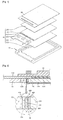
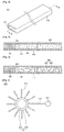
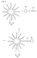
- Elément optique comprenant :un hôte (440) ;une pluralité de particules de conversion de longueur d'onde (430) disposées dans l'hôte (440) ;une pluralité de particules de réception d'électrons (460) adjacentes aux particules de conversion de longueur d'onde (430), respectivement,caractérisé en ce que l'élément optique comprend en outre :un tube (410), l'hôte (440) étant disposé dans le tube (410) ;un bouchon d'obturation (420) disposé à une extrémité du tube (410) ;une couche d'air (450) disposée entre le bouchon d'obturation (420) et l'hôte (440) ; etdes ligands de pontage (470) qui raccordent les particules de conversion de longueur d'onde (430) aux particules de réception d'électrons (460), respectivement,dans lequel certaines extrémités des ligands de pontage (470) sont liées à des ligands de stabilisation (433) des particules de conversion de longueur d'onde (430),dans lequel les autres extrémités des ligands de pontage (470) sont liées aux particules de réception d'électrons (460) .
- Elément optique selon la revendication 1, dans lequel les particules de réception d'électrons (460) comprennent des métaux.
- Elément optique selon la revendication 2, dans lequel les ligands (470) ont une longueur comprise entre environ 10 nm et environ 50 nm.
- Elément optique selon la revendication 1, dans lequel les particules de réception d'électrons (460) ont un diamètre compris entre environ 1 nm et environ 10 nm.
- Elément optique selon la revendication 1, dans lequel un rapport des particules de conversion de longueur d'onde (430) sur les particules de réception d'électrons (460) en chiffre est compris entre 4/1 et 1/4.
- Elément optique selon la revendication 1, dans lequel une distance entre les particules de conversion de longueur d'onde (430) et les particules de réception d'électrons (460) est comprise entre environ 10 nm et environ 50 nm.
- Elément optique selon la revendication 1, dans lequel la particule de conversion de longueur d'onde (430) comprend un semi-conducteur composé et la particule de réception d'électrons (460) comprend un métal.
- Elément optique selon la revendication 1, comprenant en outre un agent dispersant ajouté à l'hôte (440), dans lequel l'agent dispersant comprend un agent dispersant du pétrole au silicium, du dodécylbenzènesulfonate de sodium, du sulfosuccinate de semi-ester de nonylphénol éthoxylé disodique ou du sulfosuccinate de sodium estérique dioctylique.
- Dispositif d'affichage comprenant :une source de lumière ;un élément de conversion de longueur d'onde dans lequel la lumière est incidente à partir de la source lumineuse ;et un panneau d'affichage dans lequel la lumière est incidente à partir de l'élément de conversion de longueur d'onde, l'élément de conversion de longueur d'onde comprenant l'élément optique selon la revendication 1.
- Dispositif d'affichage selon la revendication 9, dans lequel les particules de réception d'électrons (460) comprennent AU, Ag ou Al.
- Dispositif d'affichage selon la revendication 9, dans lequel une distance entre chaque particule de conversion de longueur d'onde (430) et chaque particule de réception d'électrons (460) est comprise entre environ 10 nm et environ 50 nm.
Applications Claiming Priority (2)
| Application Number | Priority Date | Filing Date | Title |
|---|---|---|---|
| KR1020110074738A KR101916245B1 (ko) | 2011-07-27 | 2011-07-27 | 광학 부재 및 이를 포함하는 표시장치 |
| PCT/KR2012/005122 WO2013015532A2 (fr) | 2011-07-27 | 2012-06-28 | Élément optique, dispositif d'affichage et dispositif d'émission de lumière le comprenant |
Publications (3)
| Publication Number | Publication Date |
|---|---|
| EP2737345A2 EP2737345A2 (fr) | 2014-06-04 |
| EP2737345A4 EP2737345A4 (fr) | 2014-10-22 |
| EP2737345B1 true EP2737345B1 (fr) | 2016-04-27 |
Family
ID=47601600
Family Applications (1)
| Application Number | Title | Priority Date | Filing Date |
|---|---|---|---|
| EP12817716.9A Active EP2737345B1 (fr) | 2011-07-27 | 2012-06-28 | Feuille lumineuse comprenant des points quantiques et des particules métalliques pour un dispositif à écran plat |
Country Status (5)
| Country | Link |
|---|---|
| US (1) | US9574744B2 (fr) |
| EP (1) | EP2737345B1 (fr) |
| KR (1) | KR101916245B1 (fr) |
| TW (1) | TWI504979B (fr) |
| WO (1) | WO2013015532A2 (fr) |
Families Citing this family (8)
| Publication number | Priority date | Publication date | Assignee | Title |
|---|---|---|---|---|
| KR101262634B1 (ko) * | 2011-03-14 | 2013-05-08 | 엘지이노텍 주식회사 | 표시장치 |
| US20170222095A1 (en) * | 2014-08-06 | 2017-08-03 | Ns Materials Inc. | Resin molded product and manufacturing method thereof, and wavelength conversion member and illumination member |
| KR102318262B1 (ko) | 2015-03-11 | 2021-10-27 | 삼성디스플레이 주식회사 | 백라이트 유닛 및 이를 포함하는 표시 장치 |
| CN104914620B (zh) * | 2015-06-02 | 2019-01-15 | 武汉华星光电技术有限公司 | 灯条及背光模组 |
| DE102015114175A1 (de) * | 2015-08-26 | 2017-03-16 | Osram Opto Semiconductors Gmbh | Verfahren zur Herstellung von lichtemittierenden Halbleiterbauteilen und lichtemittierendes Halbleiterbauteil |
| KR20190042633A (ko) * | 2016-08-22 | 2019-04-24 | 메르크 파텐트 게엠베하 | 광학 디바이스용 혼합물 |
| KR20180036227A (ko) * | 2016-09-30 | 2018-04-09 | 삼성전자주식회사 | 양자점 유닛, 이를 포함하는 양자점 시트 및 양자점 유닛 또는 양자점 시트를 포함하는 디스플레이장치 |
| KR102627073B1 (ko) * | 2016-11-30 | 2024-01-19 | 삼성디스플레이 주식회사 | 백라이트 유닛, 표시 장치 및 표시 장치의 제조 방법 |
Family Cites Families (17)
| Publication number | Priority date | Publication date | Assignee | Title |
|---|---|---|---|---|
| US7481562B2 (en) * | 2004-11-18 | 2009-01-27 | Avago Technologies Ecbu Ip (Singapore) Pte. Ltd. | Device and method for providing illuminating light using quantum dots |
| WO2006115486A1 (fr) | 2005-04-22 | 2006-11-02 | Seldon Technologies, Llc | Article comprenant des nanotubes de carbone et procede d’utilisation de celui-ci pour purifier des fluides |
| WO2006129228A2 (fr) * | 2005-06-02 | 2006-12-07 | Philips Intellectual Property & Standards Gmbh | Systeme d'eclairage comprenant un materiau luminescent compensant une defaillance des couleurs |
| JP5245222B2 (ja) | 2005-08-10 | 2013-07-24 | 三菱化学株式会社 | 蛍光体及びそれを用いた発光装置 |
| CN101379164B (zh) | 2006-02-10 | 2012-11-21 | 三菱化学株式会社 | 荧光体及其制造方法、含荧光体的组合物、发光装置、图像显示装置和照明装置 |
| AU2007353821B2 (en) * | 2006-11-01 | 2012-09-20 | Wake Forest University | Solid state lighting compositions and systems |
| US7888700B2 (en) | 2007-03-08 | 2011-02-15 | Eastman Kodak Company | Quantum dot light emitting device |
| WO2009011922A1 (fr) | 2007-07-18 | 2009-01-22 | Qd Vision, Inc. | Feuilles de lumière à base de points quantiques utiles pour un éclairage à semi-conducteur |
| TW200912478A (en) | 2007-07-31 | 2009-03-16 | Luminus Devices Inc | Illumination assembly including wavelength converting material having spatially varying density |
| US8337029B2 (en) * | 2008-01-17 | 2012-12-25 | Intematix Corporation | Light emitting device with phosphor wavelength conversion |
| WO2009137053A1 (fr) * | 2008-05-06 | 2009-11-12 | Qd Vision, Inc. | Composants optiques, systèmes comprenant un composant optique et dispositifs associés |
| TWI373859B (en) | 2008-06-06 | 2012-10-01 | Univ Nat Taiwan | White light-emitting diode, and method for improving a white light-emitting diode |
| KR101577300B1 (ko) * | 2008-10-28 | 2015-12-15 | 삼성디스플레이 주식회사 | 양자점을 이용한 백색광 발광다이오드 구조 및 이를 포함하는 백라이트 어셈블리 |
| US8649443B2 (en) | 2009-04-28 | 2014-02-11 | Texas Instruments Incorporated | OFDM-lite architecture for HomePlug |
| KR101711085B1 (ko) * | 2009-10-09 | 2017-03-14 | 삼성전자 주식회사 | 나노 복합 입자, 그 제조방법 및 상기 나노 복합 입자를 포함하는 소자 |
| JP4991001B2 (ja) * | 2009-12-28 | 2012-08-01 | シャープ株式会社 | 照明装置 |
| KR101261461B1 (ko) * | 2010-07-14 | 2013-05-10 | 엘지이노텍 주식회사 | 액정 표시 장치 |
-
2011
- 2011-07-27 KR KR1020110074738A patent/KR101916245B1/ko active IP Right Grant
-
2012
- 2012-06-28 WO PCT/KR2012/005122 patent/WO2013015532A2/fr active Application Filing
- 2012-06-28 US US14/235,329 patent/US9574744B2/en active Active
- 2012-06-28 EP EP12817716.9A patent/EP2737345B1/fr active Active
- 2012-07-06 TW TW101124379A patent/TWI504979B/zh active
Also Published As
| Publication number | Publication date |
|---|---|
| WO2013015532A2 (fr) | 2013-01-31 |
| WO2013015532A3 (fr) | 2013-03-21 |
| EP2737345A4 (fr) | 2014-10-22 |
| TW201305673A (zh) | 2013-02-01 |
| KR20130013217A (ko) | 2013-02-06 |
| US20140160727A1 (en) | 2014-06-12 |
| EP2737345A2 (fr) | 2014-06-04 |
| TWI504979B (zh) | 2015-10-21 |
| KR101916245B1 (ko) | 2018-11-07 |
| US9574744B2 (en) | 2017-02-21 |
Similar Documents
| Publication | Publication Date | Title |
|---|---|---|
| US9778409B2 (en) | Optical member, display device, and light emitting device having the same | |
| EP2737345B1 (fr) | Feuille lumineuse comprenant des points quantiques et des particules métalliques pour un dispositif à écran plat | |
| EP2776875B1 (fr) | Dispositif d'affichage comprenant élément de conversion de la lumière | |
| TWI447489B (zh) | 顯示裝置 | |
| US9720159B2 (en) | Optical member and display device including the same | |
| JP2013536460A (ja) | 表示装置 | |
| EP2734875B1 (fr) | Élément optique et dispositif d'affichage le comportant | |
| KR101251811B1 (ko) | 파장 변환 복합체, 이를 포함하는 발광 소자 및 표시장치 및 이의 제조방법 | |
| KR20130065484A (ko) | 광 변환 복합체, 이를 포함하는 발광장치 및 표시장치 및 이의 제조방법 | |
| KR101862873B1 (ko) | 광학 부재, 발광장치 및 표시장치 | |
| KR101956079B1 (ko) | 발광 장치 및 표시 장치 | |
| KR101326892B1 (ko) | 광학 부재, 이를 포함하는 발광장치 및 표시장치 및 이의 제조방법 | |
| KR101294545B1 (ko) | 광 변환 복합체, 이를 포함하는 발광장치 및 표시장치 및 이의 제조방법 | |
| KR101934419B1 (ko) | 광 변환 복합체, 이를 포함하는 발광장치 및 표시장치 및 이의 제조방법 | |
| KR101877485B1 (ko) | 광 변환 부재, 이를 포함하는 발광장치 및 표시장치 | |
| KR20130110947A (ko) | 광 변환 복합체, 이를 포함하는 발광장치 및 표시장치 및 이의 제조방법 | |
| KR101327027B1 (ko) | 광 변환 복합체, 이를 포함하는 발광장치 및 표시장치 및 이의 제조방법 | |
| KR20130010382A (ko) | 광학 부재, 이를 포함하는 표시장치 및 이의 제조방법 | |
| KR20130050181A (ko) | 표시장치 |
Legal Events
| Date | Code | Title | Description |
|---|---|---|---|
| PUAI | Public reference made under article 153(3) epc to a published international application that has entered the european phase |
Free format text: ORIGINAL CODE: 0009012 |
|
| 17P | Request for examination filed |
Effective date: 20140128 |
|
| AK | Designated contracting states |
Kind code of ref document: A2 Designated state(s): AL AT BE BG CH CY CZ DE DK EE ES FI FR GB GR HR HU IE IS IT LI LT LU LV MC MK MT NL NO PL PT RO RS SE SI SK SM TR |
|
| REG | Reference to a national code |
Ref country code: DE Ref legal event code: R079 Ref document number: 602012017898 Country of ref document: DE Free format text: PREVIOUS MAIN CLASS: G02B0005230000 Ipc: G02F0001133500 |
|
| A4 | Supplementary search report drawn up and despatched |
Effective date: 20140924 |
|
| RIC1 | Information provided on ipc code assigned before grant |
Ipc: C09K 11/56 20060101ALI20140918BHEP Ipc: C09K 11/02 20060101ALI20140918BHEP Ipc: G02B 6/00 20060101ALI20140918BHEP Ipc: H01L 33/50 20100101ALI20140918BHEP Ipc: F21V 9/16 20060101ALI20140918BHEP Ipc: G02F 1/1335 20060101AFI20140918BHEP Ipc: C09K 11/88 20060101ALI20140918BHEP |
|
| DAX | Request for extension of the european patent (deleted) | ||
| 17Q | First examination report despatched |
Effective date: 20150416 |
|
| GRAP | Despatch of communication of intention to grant a patent |
Free format text: ORIGINAL CODE: EPIDOSNIGR1 |
|
| INTG | Intention to grant announced |
Effective date: 20151110 |
|
| GRAS | Grant fee paid |
Free format text: ORIGINAL CODE: EPIDOSNIGR3 |
|
| GRAA | (expected) grant |
Free format text: ORIGINAL CODE: 0009210 |
|
| AK | Designated contracting states |
Kind code of ref document: B1 Designated state(s): AL AT BE BG CH CY CZ DE DK EE ES FI FR GB GR HR HU IE IS IT LI LT LU LV MC MK MT NL NO PL PT RO RS SE SI SK SM TR |
|
| REG | Reference to a national code |
Ref country code: GB Ref legal event code: FG4D |
|
| REG | Reference to a national code |
Ref country code: CH Ref legal event code: EP |
|
| REG | Reference to a national code |
Ref country code: AT Ref legal event code: REF Ref document number: 795426 Country of ref document: AT Kind code of ref document: T Effective date: 20160515 |
|
| REG | Reference to a national code |
Ref country code: IE Ref legal event code: FG4D |
|
| REG | Reference to a national code |
Ref country code: DE Ref legal event code: R096 Ref document number: 602012017898 Country of ref document: DE |
|
| REG | Reference to a national code |
Ref country code: FR Ref legal event code: PLFP Year of fee payment: 5 |
|
| REG | Reference to a national code |
Ref country code: LT Ref legal event code: MG4D |
|
| REG | Reference to a national code |
Ref country code: NL Ref legal event code: MP Effective date: 20160427 |
|
| REG | Reference to a national code |
Ref country code: AT Ref legal event code: MK05 Ref document number: 795426 Country of ref document: AT Kind code of ref document: T Effective date: 20160427 |
|
| PG25 | Lapsed in a contracting state [announced via postgrant information from national office to epo] |
Ref country code: NL Free format text: LAPSE BECAUSE OF FAILURE TO SUBMIT A TRANSLATION OF THE DESCRIPTION OR TO PAY THE FEE WITHIN THE PRESCRIBED TIME-LIMIT Effective date: 20160427 |
|
| PG25 | Lapsed in a contracting state [announced via postgrant information from national office to epo] |
Ref country code: LT Free format text: LAPSE BECAUSE OF FAILURE TO SUBMIT A TRANSLATION OF THE DESCRIPTION OR TO PAY THE FEE WITHIN THE PRESCRIBED TIME-LIMIT Effective date: 20160427 Ref country code: FI Free format text: LAPSE BECAUSE OF FAILURE TO SUBMIT A TRANSLATION OF THE DESCRIPTION OR TO PAY THE FEE WITHIN THE PRESCRIBED TIME-LIMIT Effective date: 20160427 Ref country code: PL Free format text: LAPSE BECAUSE OF FAILURE TO SUBMIT A TRANSLATION OF THE DESCRIPTION OR TO PAY THE FEE WITHIN THE PRESCRIBED TIME-LIMIT Effective date: 20160427 Ref country code: NO Free format text: LAPSE BECAUSE OF FAILURE TO SUBMIT A TRANSLATION OF THE DESCRIPTION OR TO PAY THE FEE WITHIN THE PRESCRIBED TIME-LIMIT Effective date: 20160727 |
|
| PG25 | Lapsed in a contracting state [announced via postgrant information from national office to epo] |
Ref country code: ES Free format text: LAPSE BECAUSE OF FAILURE TO SUBMIT A TRANSLATION OF THE DESCRIPTION OR TO PAY THE FEE WITHIN THE PRESCRIBED TIME-LIMIT Effective date: 20160427 Ref country code: GR Free format text: LAPSE BECAUSE OF FAILURE TO SUBMIT A TRANSLATION OF THE DESCRIPTION OR TO PAY THE FEE WITHIN THE PRESCRIBED TIME-LIMIT Effective date: 20160728 Ref country code: SE Free format text: LAPSE BECAUSE OF FAILURE TO SUBMIT A TRANSLATION OF THE DESCRIPTION OR TO PAY THE FEE WITHIN THE PRESCRIBED TIME-LIMIT Effective date: 20160427 Ref country code: LV Free format text: LAPSE BECAUSE OF FAILURE TO SUBMIT A TRANSLATION OF THE DESCRIPTION OR TO PAY THE FEE WITHIN THE PRESCRIBED TIME-LIMIT Effective date: 20160427 Ref country code: HR Free format text: LAPSE BECAUSE OF FAILURE TO SUBMIT A TRANSLATION OF THE DESCRIPTION OR TO PAY THE FEE WITHIN THE PRESCRIBED TIME-LIMIT Effective date: 20160427 Ref country code: AT Free format text: LAPSE BECAUSE OF FAILURE TO SUBMIT A TRANSLATION OF THE DESCRIPTION OR TO PAY THE FEE WITHIN THE PRESCRIBED TIME-LIMIT Effective date: 20160427 Ref country code: RS Free format text: LAPSE BECAUSE OF FAILURE TO SUBMIT A TRANSLATION OF THE DESCRIPTION OR TO PAY THE FEE WITHIN THE PRESCRIBED TIME-LIMIT Effective date: 20160427 Ref country code: PT Free format text: LAPSE BECAUSE OF FAILURE TO SUBMIT A TRANSLATION OF THE DESCRIPTION OR TO PAY THE FEE WITHIN THE PRESCRIBED TIME-LIMIT Effective date: 20160829 |
|
| PG25 | Lapsed in a contracting state [announced via postgrant information from national office to epo] |
Ref country code: BE Free format text: LAPSE BECAUSE OF FAILURE TO SUBMIT A TRANSLATION OF THE DESCRIPTION OR TO PAY THE FEE WITHIN THE PRESCRIBED TIME-LIMIT Effective date: 20160427 Ref country code: IT Free format text: LAPSE BECAUSE OF FAILURE TO SUBMIT A TRANSLATION OF THE DESCRIPTION OR TO PAY THE FEE WITHIN THE PRESCRIBED TIME-LIMIT Effective date: 20160427 |
|
| REG | Reference to a national code |
Ref country code: DE Ref legal event code: R097 Ref document number: 602012017898 Country of ref document: DE |
|
| PG25 | Lapsed in a contracting state [announced via postgrant information from national office to epo] |
Ref country code: RO Free format text: LAPSE BECAUSE OF FAILURE TO SUBMIT A TRANSLATION OF THE DESCRIPTION OR TO PAY THE FEE WITHIN THE PRESCRIBED TIME-LIMIT Effective date: 20160427 Ref country code: DK Free format text: LAPSE BECAUSE OF FAILURE TO SUBMIT A TRANSLATION OF THE DESCRIPTION OR TO PAY THE FEE WITHIN THE PRESCRIBED TIME-LIMIT Effective date: 20160427 Ref country code: MC Free format text: LAPSE BECAUSE OF FAILURE TO SUBMIT A TRANSLATION OF THE DESCRIPTION OR TO PAY THE FEE WITHIN THE PRESCRIBED TIME-LIMIT Effective date: 20160427 Ref country code: EE Free format text: LAPSE BECAUSE OF FAILURE TO SUBMIT A TRANSLATION OF THE DESCRIPTION OR TO PAY THE FEE WITHIN THE PRESCRIBED TIME-LIMIT Effective date: 20160427 Ref country code: CZ Free format text: LAPSE BECAUSE OF FAILURE TO SUBMIT A TRANSLATION OF THE DESCRIPTION OR TO PAY THE FEE WITHIN THE PRESCRIBED TIME-LIMIT Effective date: 20160427 Ref country code: SK Free format text: LAPSE BECAUSE OF FAILURE TO SUBMIT A TRANSLATION OF THE DESCRIPTION OR TO PAY THE FEE WITHIN THE PRESCRIBED TIME-LIMIT Effective date: 20160427 |
|
| REG | Reference to a national code |
Ref country code: CH Ref legal event code: PL |
|
| PG25 | Lapsed in a contracting state [announced via postgrant information from national office to epo] |
Ref country code: SM Free format text: LAPSE BECAUSE OF FAILURE TO SUBMIT A TRANSLATION OF THE DESCRIPTION OR TO PAY THE FEE WITHIN THE PRESCRIBED TIME-LIMIT Effective date: 20160427 |
|
| PLBE | No opposition filed within time limit |
Free format text: ORIGINAL CODE: 0009261 |
|
| STAA | Information on the status of an ep patent application or granted ep patent |
Free format text: STATUS: NO OPPOSITION FILED WITHIN TIME LIMIT |
|
| GBPC | Gb: european patent ceased through non-payment of renewal fee |
Effective date: 20160727 |
|
| REG | Reference to a national code |
Ref country code: IE Ref legal event code: MM4A |
|
| 26N | No opposition filed |
Effective date: 20170130 |
|
| PG25 | Lapsed in a contracting state [announced via postgrant information from national office to epo] |
Ref country code: LI Free format text: LAPSE BECAUSE OF NON-PAYMENT OF DUE FEES Effective date: 20160630 Ref country code: CH Free format text: LAPSE BECAUSE OF NON-PAYMENT OF DUE FEES Effective date: 20160630 |
|
| REG | Reference to a national code |
Ref country code: FR Ref legal event code: PLFP Year of fee payment: 6 |
|
| PG25 | Lapsed in a contracting state [announced via postgrant information from national office to epo] |
Ref country code: SI Free format text: LAPSE BECAUSE OF FAILURE TO SUBMIT A TRANSLATION OF THE DESCRIPTION OR TO PAY THE FEE WITHIN THE PRESCRIBED TIME-LIMIT Effective date: 20160427 Ref country code: IE Free format text: LAPSE BECAUSE OF NON-PAYMENT OF DUE FEES Effective date: 20160628 Ref country code: GB Free format text: LAPSE BECAUSE OF NON-PAYMENT OF DUE FEES Effective date: 20160727 |
|
| REG | Reference to a national code |
Ref country code: FR Ref legal event code: PLFP Year of fee payment: 7 |
|
| PG25 | Lapsed in a contracting state [announced via postgrant information from national office to epo] |
Ref country code: HU Free format text: LAPSE BECAUSE OF FAILURE TO SUBMIT A TRANSLATION OF THE DESCRIPTION OR TO PAY THE FEE WITHIN THE PRESCRIBED TIME-LIMIT; INVALID AB INITIO Effective date: 20120628 |
|
| PG25 | Lapsed in a contracting state [announced via postgrant information from national office to epo] |
Ref country code: LU Free format text: LAPSE BECAUSE OF NON-PAYMENT OF DUE FEES Effective date: 20160628 Ref country code: CY Free format text: LAPSE BECAUSE OF FAILURE TO SUBMIT A TRANSLATION OF THE DESCRIPTION OR TO PAY THE FEE WITHIN THE PRESCRIBED TIME-LIMIT Effective date: 20160427 Ref country code: MK Free format text: LAPSE BECAUSE OF FAILURE TO SUBMIT A TRANSLATION OF THE DESCRIPTION OR TO PAY THE FEE WITHIN THE PRESCRIBED TIME-LIMIT Effective date: 20160427 Ref country code: MT Free format text: LAPSE BECAUSE OF NON-PAYMENT OF DUE FEES Effective date: 20160630 Ref country code: IS Free format text: LAPSE BECAUSE OF FAILURE TO SUBMIT A TRANSLATION OF THE DESCRIPTION OR TO PAY THE FEE WITHIN THE PRESCRIBED TIME-LIMIT Effective date: 20160427 |
|
| PG25 | Lapsed in a contracting state [announced via postgrant information from national office to epo] |
Ref country code: BG Free format text: LAPSE BECAUSE OF FAILURE TO SUBMIT A TRANSLATION OF THE DESCRIPTION OR TO PAY THE FEE WITHIN THE PRESCRIBED TIME-LIMIT Effective date: 20160427 |
|
| PG25 | Lapsed in a contracting state [announced via postgrant information from national office to epo] |
Ref country code: AL Free format text: LAPSE BECAUSE OF FAILURE TO SUBMIT A TRANSLATION OF THE DESCRIPTION OR TO PAY THE FEE WITHIN THE PRESCRIBED TIME-LIMIT Effective date: 20160427 Ref country code: TR Free format text: LAPSE BECAUSE OF FAILURE TO SUBMIT A TRANSLATION OF THE DESCRIPTION OR TO PAY THE FEE WITHIN THE PRESCRIBED TIME-LIMIT Effective date: 20160427 |
|
| PGFP | Annual fee paid to national office [announced via postgrant information from national office to epo] |
Ref country code: FR Payment date: 20230522 Year of fee payment: 12 Ref country code: DE Payment date: 20230522 Year of fee payment: 12 |