EP2736148B1 - Non-contact power supply system - Google Patents
Non-contact power supply system Download PDFInfo
- Publication number
- EP2736148B1 EP2736148B1 EP12814139.7A EP12814139A EP2736148B1 EP 2736148 B1 EP2736148 B1 EP 2736148B1 EP 12814139 A EP12814139 A EP 12814139A EP 2736148 B1 EP2736148 B1 EP 2736148B1
- Authority
- EP
- European Patent Office
- Prior art keywords
- resonance
- frequency
- power supply
- power
- reception device
- Prior art date
- Legal status (The legal status is an assumption and is not a legal conclusion. Google has not performed a legal analysis and makes no representation as to the accuracy of the status listed.)
- Active
Links
- 239000003990 capacitor Substances 0.000 claims description 14
- 230000004907 flux Effects 0.000 claims description 5
- 230000007423 decrease Effects 0.000 description 9
- 230000005284 excitation Effects 0.000 description 5
- 230000005540 biological transmission Effects 0.000 description 3
- 230000003247 decreasing effect Effects 0.000 description 3
- 230000008878 coupling Effects 0.000 description 2
- 238000010168 coupling process Methods 0.000 description 2
- 238000005859 coupling reaction Methods 0.000 description 2
- 230000001939 inductive effect Effects 0.000 description 2
- 238000010586 diagram Methods 0.000 description 1
- 230000005674 electromagnetic induction Effects 0.000 description 1
Images

Classifications
-
- H—ELECTRICITY
- H02—GENERATION; CONVERSION OR DISTRIBUTION OF ELECTRIC POWER
- H02J—CIRCUIT ARRANGEMENTS OR SYSTEMS FOR SUPPLYING OR DISTRIBUTING ELECTRIC POWER; SYSTEMS FOR STORING ELECTRIC ENERGY
- H02J7/00—Circuit arrangements for charging or depolarising batteries or for supplying loads from batteries
- H02J7/0042—Circuit arrangements for charging or depolarising batteries or for supplying loads from batteries characterised by the mechanical construction
- H02J7/0044—Circuit arrangements for charging or depolarising batteries or for supplying loads from batteries characterised by the mechanical construction specially adapted for holding portable devices containing batteries
-
- H—ELECTRICITY
- H01—ELECTRIC ELEMENTS
- H01F—MAGNETS; INDUCTANCES; TRANSFORMERS; SELECTION OF MATERIALS FOR THEIR MAGNETIC PROPERTIES
- H01F38/00—Adaptations of transformers or inductances for specific applications or functions
- H01F38/14—Inductive couplings
-
- H—ELECTRICITY
- H01—ELECTRIC ELEMENTS
- H01M—PROCESSES OR MEANS, e.g. BATTERIES, FOR THE DIRECT CONVERSION OF CHEMICAL ENERGY INTO ELECTRICAL ENERGY
- H01M10/00—Secondary cells; Manufacture thereof
- H01M10/42—Methods or arrangements for servicing or maintenance of secondary cells or secondary half-cells
- H01M10/46—Accumulators structurally combined with charging apparatus
-
- H—ELECTRICITY
- H02—GENERATION; CONVERSION OR DISTRIBUTION OF ELECTRIC POWER
- H02J—CIRCUIT ARRANGEMENTS OR SYSTEMS FOR SUPPLYING OR DISTRIBUTING ELECTRIC POWER; SYSTEMS FOR STORING ELECTRIC ENERGY
- H02J50/00—Circuit arrangements or systems for wireless supply or distribution of electric power
- H02J50/10—Circuit arrangements or systems for wireless supply or distribution of electric power using inductive coupling
- H02J50/12—Circuit arrangements or systems for wireless supply or distribution of electric power using inductive coupling of the resonant type
-
- H—ELECTRICITY
- H02—GENERATION; CONVERSION OR DISTRIBUTION OF ELECTRIC POWER
- H02J—CIRCUIT ARRANGEMENTS OR SYSTEMS FOR SUPPLYING OR DISTRIBUTING ELECTRIC POWER; SYSTEMS FOR STORING ELECTRIC ENERGY
- H02J50/00—Circuit arrangements or systems for wireless supply or distribution of electric power
- H02J50/90—Circuit arrangements or systems for wireless supply or distribution of electric power involving detection or optimisation of position, e.g. alignment
-
- H04B5/79—
-
- Y—GENERAL TAGGING OF NEW TECHNOLOGICAL DEVELOPMENTS; GENERAL TAGGING OF CROSS-SECTIONAL TECHNOLOGIES SPANNING OVER SEVERAL SECTIONS OF THE IPC; TECHNICAL SUBJECTS COVERED BY FORMER USPC CROSS-REFERENCE ART COLLECTIONS [XRACs] AND DIGESTS
- Y02—TECHNOLOGIES OR APPLICATIONS FOR MITIGATION OR ADAPTATION AGAINST CLIMATE CHANGE
- Y02E—REDUCTION OF GREENHOUSE GAS [GHG] EMISSIONS, RELATED TO ENERGY GENERATION, TRANSMISSION OR DISTRIBUTION
- Y02E60/00—Enabling technologies; Technologies with a potential or indirect contribution to GHG emissions mitigation
- Y02E60/10—Energy storage using batteries
Description
- The present invention relates to a non-contact power supply system that supplies power to the power reception device in a non-contact manner.
- In the prior art, a non-contact power supply system supplies power in a non-contact manner from a power supply device to a power reception device (see for example
JP 2003-204637 A - Over these recent years, to improve user convenience, study has been conducted to develop a free layout type non-contact power supply system that allows for the power reception device to be supplied with power by arranging the power reception device at any position on the upper surface (power supplying surface) of the power supply device (see for example
JP 2008-005573 A -
US 7,880,337 B2 shows a high power wireless resonant energy transfer system that transfers energy across an airgap. An energy reception system is positioned to receive the transferred energy across the airgap through a resonant inductive coupling between the transmission and reception system. The energy transmission system is arranged to automatically and electronically vary the spatial direction of the resonant inductive coupling with the alignment between the transmission and reception system, such that energy transfer occurs at a desired location, frequency and power level.. -
US 2004/0130916 A1 relates to a contactless power supply that has a dynamically configurable tank circuit powered by an inverter. The contactless power supply is inductively coupled to one or more loads. The inverter is connected to a DC power source. When loads are added or removed from the system, the contactless power supply is capable of modifying the resonant frequency of the tank circuit, the inverter frequency, the inverter duty cycle or the rail voltage of the DC power source. - As shown in
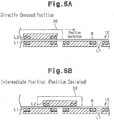
Fig. 5A , in a free layout type non-contact power supply system, primary coils L1 are arranged in apower supply device 10 along apower supply surface 6 of thepower supply device 10. Apower reception device 30 includes a secondary coil L2. InFig. 5A , the secondary coil L2 is directly opposed to a primary coil L1. The primary coil L1 is excited at an operational frequency f1. A change in the magnetic flux from the excited primary coil L1 induces current at the secondary coil L2. The induced current becomes the output power of thepower reception device 30. In this manner, electromagnetic induction is used to supply power from thepower supply device 10 to thepower reception device 30. - In a non-contact power supply system of the prior art (system that is not of a free layout type), as shown in
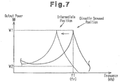
Fig. 7 , the operational frequency f1 of the primary coil L1 is set to conform to a resonance frequency fr of a resonance system when the secondary coil L2 is directly opposed to the primary coil L1. The resonance frequency fr is the resonance frequency of the secondary coil L2. In the non-contact power supply system of the prior art, the power reception device is arranged at a determined position relative to the power supply device. This allows for the secondary coil to be directly opposed to the primary coil when supplying power. Thus, by setting the operational frequency f1 at the resonance frequency fr, thepower reception device 30 may obtain the maximum output power W1. - In the free layout type non-contact power supply system, the
power reception device 30 does not have to be arranged at any particular position as long as it is arranged on thepower supply surface 6. Thus, as shown inFig. 5B , the secondary coil L2 may be arranged at an intermediate position between two primary coils L1. When the secondary coil L2 is located at a position directly opposed to a primary coil L1, the leakage inductance Le is minimal. The leakage inductance Le increases as the secondary coil L2 becomes farther along thepower supply surface 6 from a directly opposed position. - It is known that the resonance frequency fr decreases as the leakage inductance Le increases. Thus, as shown by the arrow in
Fig. 7 , the resonance frequency fr of the resonance system decreases in accordance with the positional deviation of the secondary coil L2 from the primary coil L1. Thus, the output power at an intermediate position between primary coils L1 becomes output power W2, which is drastically decreased from output power W1 obtained at the directly opposed position. In this manner, in the free layout type non-contact power supply system, the output power of thepower reception device 30 varies greatly depending on where thepower reception device 30 is located, and it is difficult to obtain stable output power. - Accordingly, it is an object of the present invention to provide a non-contact power supply system that allows for stable output power to be obtained regardless of where a secondary coil is located.
- One aspect of the present invention is a non-contact power supply system including a power supply device, which includes primary coils arranged on a power supply surface and configured to be excited at an operational frequency, and a power reception device, which includes a secondary coil configured to induce current using resonance phenomenon based on alternating flux from the primary coils when arranged on the power supply surface. In the non-contact power supply system, the operational frequency that excites the primary coil is set at or in the proximity of a resonance frequency of a resonance system formed when the secondary coil is located at an intermediate position between two of the primary coils that are adjacent to each other. In the above configuration, the power reception device includes a capacitor connected to the secondary coil. In this configuration, the capacitance of the capacitor is adjusted to set a position of a resonance system for the operational frequency that excites the primary coil. The operational frequency is set in the proximity of the resonance frequency of the resonance system corresponding to the intermediate position. The proximity of the resonance frequency is a frequency region at which output power of the power reception device obtained by the resonance system corresponding to the intermediate position is greater than or equal to an output power of the power reception device obtained by a resonance system formed when the secondary coil is located at a position directly opposed to one of the primary coils.
- In the above configuration, preferably, in the proximity of the resonance frequency at the resonance system of the intermediate position, the operational frequency is set to differ from the resonance frequency.
-
-
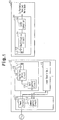
Fig. 1 is a block diagram showing the configuration of a non-contact power supply system; -
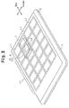
Fig. 2 is a perspective view of a power supply device; -
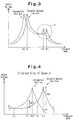
Fig. 3 is a graph showing a resonance system including primary and secondary frequencies; -
Fig. 4 is an enlarged view of the resonance curve in range A ofFig. 3 ; -
Fig. 5A is a partial cross-sectional view of a power supply device and a power reception device when a secondary coil L2 is located at a directly opposed position, andFig. 5B is a partial cross-sectional view of the power supply device and the power reception device when the secondary coil L2 is located at an intermediate position; -
Fig. 6A is a graph showing the output power of the power reception device in correspondence with the position of the secondary coil L2 in the setting of a prior art resonance system, andFig. 6B is a graph showing the output power of the power reception device in correspondence with the position of the secondary coil L2 in the setting of the resonance system of the present invention; and -
Fig. 7 is a graph for a non-contact power supply system of the background art showing a resonance system when the secondary coil is located at a directly opposed position and when the secondary coil is located at an intermediate position. - One embodiment of a non-contact power supply system will now be described with reference to
Figs. 1 to 6 . - As shown in
Fig. 1 , the non-contact power supply system includes apower supply device 10 and apower reception device 30. In the present example, thepower reception device 30 is incorporated in aportable terminal 40. The detailed configurations of thepower supply device 10 and thepower reception device 30 will now be described. - As shown in
Fig. 2 , thepower supply device 10 includes a planar case 5. The case 5 includes an upper surface that defines apower supply surface 6 on which theportable terminal 40 is arranged. Primary coils L1 are arranged throughout the entire region of thepower supply surface 6 in the case 5. In the present example, twenty-four primary coils L1 are arranged in four rows and six columns in a matrix-like manner in thepower supply surface 6. - As shown in
Fig. 1 , thepower supply device 10 includes a singlecommon unit 11 and a plurality of (in the present example, twenty-four, which is the same number as the primary coils L1)power supply units 15. - The
common unit 11 includes apower circuit 13 and a common control circuit 12. Thepower circuit 13 converts AC power from an external power source to suitable DC voltage and supplies the DC voltage as operational power to eachpower supply unit 15 and thecommon unit 11. - The common control circuit 12, which is configured by a microcomputer, centrally controls the
power supply device 10 by providing various command signals to eachpower supply unit 15. - The
power supply unit 15 includes aunit control circuit 19, anexcitation drive circuit 16, and a primary coil L1. - When the
unit control circuit 19 receives a command signal from the common control circuit 12 requesting for the supply of power, theunit control circuit 19 controls theexcitation drive circuit 16. - The two ends of the primary coil L1 is connected to the
excitation drive circuit 16. A capacitor C1 is connected between one end of the primary coil L1 and theexcitation drive circuit 16. Theexcitation drive circuit 16 generates AC current having operational frequency f1 under the control of theunit control circuit 19 and supplies the primary coil L1 and the capacitor C1 with the AC current. This excites the primary coil L1. Here, the magnetic flux generated from the primary coil L1 changes. - As shown in
Fig. 1 , thepower reception device 30 includes arectification circuit 31 and a DC/DC converter 35. - Two ends of a secondary coil L2 are connected to the
rectification circuit 31. A capacitor C2 is connected between one end of the secondary coil L2 and therectification circuit 31. The secondary coil L2 induces current based on changes in the magnetic flux from a primary coil L1. Therectification circuit 31 rectifies DC voltage induced by the secondary coil L2. The DC/DC converter 35 converts DC voltage from therectification circuit 31 to a value suitable for the operation of theportable terminal 40. The DC voltage may be used, for example, to charge a rechargeable battery (not shown), which is the operational power source of theportable terminal 40. - The resonant characteristics of the non-contact power supply system will now be described.
-
Fig. 3 is a graph for a resonance system showing the output power of thepower reception device 30 in correspondence with the operational frequency of the primary coil L1. As shown inFig. 3 , the resonance system of the present embodiment includes two resonance frequencies, namely, a primary resonance frequency fa1 and a secondary resonance frequency fb1. The primary resonance frequency fa1 is lower than the secondary resonance frequency fb1. The resonance frequencies fa1 and fb1 are the resonance frequencies when the secondary coil L2 is located at a position directly opposed to a primary coil L1. - When the operational frequency f1 that excites the primary coil L1 is set as the primary resonance frequency fa1, the impedance excessively decreases when the two coils L1 and L2 are magnetically coupled. Accordingly, to use the secondary resonance frequency fb1 in the present example, the operation frequency f1 that excites the primary coil L1 is set in the proximity of the secondary resonance frequency fb1. By setting the operational frequency f1 in the proximity of the secondary resonance frequency fb1, excessive decrease of the impedance is suppressed. The resonance frequency is obtained from the following equation.
Equation 1
- It is apparent from equation (1) that the resonance frequency decreases as the leakage inductance Le or the capacitance C of the capacitor increases. For example, when the secondary coil L2 is shifted in the planar direction of the
power supply surface 6 from the position ofFig. 5A directly opposed to the primary coil L1, the shifting increases the leakage inductance Le. In this case, the resonance system (resonance curve) shown by the solid lines inFig. 3 is moved in the direction in which the resonance frequency decreases. As shown inFig. 5B , when the secondary coil L2 is arranged at an intermediate position, which is located at a middle position between two adjacent primary coils L1, the resonance system (resonance curve) is set at the frequency shown by the broken lines inFig. 3 . In this manner, the primary resonance frequency fa2 and the secondary resonance frequency fb2 at the intermediate position are respectively smaller than the secondary resonance frequency fa1 and the secondary resonance frequency fb2. - As shown by equation (1), adjustment of the capacitance C of the capacitor C2 allows the resonance frequency (frequency region of resonance region) for the operation frequency f1 to be set. In this case, the operational frequency f1 may be fixed.
-
Fig. 4 is an enlarged view of the resonance curve in range A ofFig. 3 . As shown inFig. 4 , in the same manner as the background art described above, when the operation frequency f1 is set as the resonance frequency fb1 at the directly opposed position, the difference ΔW1 becomes maximal between the output power of thepower reception device 30 at the intermediate position and the output power of thepower reception device 30 at the directly opposed position. In this case, as shown by the graph ofFig. 6A , the output power of thepower reception device 30 is maximal (approximately 50 W) at the directly opposed position. When the secondary coil L2 is located at a middle position between the directly opposed position and the intermediate position, the output power of thepower reception device 30 is less than 20 W. When the secondary coil L2 is located at the intermediate position, the output power of thepower reception device 30 is approximately 10 W. Accordingly, when the operational frequency f1 is set as the resonance frequency fb1 at the directly opposed position, the output power when the secondary coil L2 is located at the intermediate position is decreased to approximately 20% of the output power at the directly opposed position. - In the present embodiment, the capacitance C of the capacitor C2 is adjusted to set the position of the resonance system for the operational frequency f1 so that the difference decreases between the output power of the
power reception device 30 at the intermediate position and the output power of thepower reception device 30 at the directly opposed position. In the present example, the operational frequency f1 is set in the proximity of the resonance frequency fb2 at the intermediate position. As shown inFig. 4 , the proximity of the resonance frequency fb2 is the frequency region between two intersecting points fx and fy of the resonance system corresponding to the intermediate position (resonance curve shown by broken lines) and the resonance system corresponding to the directly opposed position (resonance curve shown by solid lines). That is, the resonance system of the present embodiment is set so that the operational frequency f1 is located between the two intersecting points fx and fy. When the operational frequency f1 is set between the two intersecting points fx and fy, the output power at the intermediate position becomes greater than or equal to the directly opposed position. - When the operational frequency f1 is set in the proximity of the resonance frequency fb2, the difference ΔW2 of the output power of the
power reception device 30 at the intermediate position and the output power of thepower reception device 30 at the intermediate position becomes smaller than the difference ΔW1. In this case, as shown by the graph ofFig. 6B , the output power of thepower reception device 30 is maximal (approximately 40 W) at the intermediate position. When the secondary coil L2 is located at an intermediate position between the directly opposed position and the intermediate position, the output power of thepower reception device 30 is approximately 30 W. Further, when the secondary coil L2 is located at the directly opposed position, the output power of thepower reception device 30 is approximately 20 W. Accordingly, in this configuration, the decrease rate of the output voltage from the directly opposed position to the intermediate position is only about 50%. This allows for thepower reception device 30 to obtain further stable output power regardless of the position of the secondary coil L2. - The non-contact power supply system of the present embodiment has the advantages described below.
- (1) The operation frequency f1 is set in the proximity of the resonance frequency fb2 at the intermediate position. Thus, in comparison with when, for example, the operation frequency f1 is set as the resonance frequency at the directly opposed position, the output power difference of the
power reception device 30 between the intermediate position and the directly opposed position becomes small. Thus, further stable output power may be obtained from thepower reception device 30 regardless of where the secondary coil L2 is located. - (2) Adjustment of the capacitance of the capacitor C2 sets the position of the resonance system for the operational frequency f1. Thus, for example, even when the operational frequency f1 is specified in advance by a standard or the like, while fixing the operational frequency f1 in compliance with the standard, further stable output power of the
power reception device 30 may be obtained. - (3) Further, the operational frequency f1 is set to differ from the resonance frequency fb2 at the intermediate position. When the operational frequency f1 conforms to the resonance frequency fb2 at the intermediate position, the output power difference of the
power reception device 30 becomes large although this is not as large as when the operation frequency f1 conforms to the resonance frequency fb1 as the directly opposed position. Accordingly, the output power difference of thepower reception device 30 may be further decreased by setting the operational frequency f1 differently from the resonance frequency fb2 at the intermediate position. - The above embodiment may be modified to the forms described below.
- In the above embodiment, the capacitance C of the capacitor C2 is adjusted to set the position of the resonance system for the operational frequency f1. However, the operational frequency f1 may be changed to set the operational frequency f1 in the proximity of the resonance frequency fb2 at the intermediate position.
- In the above embodiment, the proximity of the resonance frequency fb2 is the frequency region between two intersecting points fx and fy of the resonance curve corresponding to the intermediate position and the resonance curve corresponding to the directly opposed position. However, as long as the output power difference of the
power reception device 30 decreases between the intermediate position and the directly opposed position compared to when the operation frequency f1 is set as the resonance frequency fb1, the operational frequency f1 does not have to be set to this frequency region f1. For example, the operational frequency f1 may be set to a smaller frequency region than the intersecting point fx, and the operational frequency f1 may be set to a larger frequency region than the intersecting point fy. That is, the frequency region in the proximity of the resonance frequency fb2 may be a wider range. - The resonance system may be set at a position where the operational frequency f1 conforms to the resonance frequency fb2 at the intermediate position. This also obtains a stable output voltage in comparison to when the operational frequency f1 is set to the proximity of the resonance frequency fb1 (in particular, frequency region that is higher than the resonance frequency fb1).
- In the above embodiment, the
unit control circuit 19 may be omitted. In this case, the common control circuit 12 also performs the control executed by theunit control circuit 19 in the above embodiment. Further, some of the control performed by theunit control circuit 19 may be performed by the common control circuit 12, and some of the control performed by the common control circuit 12 may be performed by theunit control circuit 19. - In the above embodiment, coil L1 and the capacitor C1 are connected in series but may be connected in parallel. Further, the coil L2 and the capacitor C2 are connected in series but may be connected in parallel.
Claims (2)
- A non-contact power supply system comprising:a power supply device (10), which includes primary coils (L1) arranged on a power supply surface (6) and configured to be excited at an operational frequency (f1), anda power reception device (30), which includes a secondary coil (L2) configured to induce current using a resonance phenomenon based on alternating flux from the primary coils (L1) when arranged on the power supply surface (6),characterized in that:the power reception device (30) further comprises a capacitor (C2) connected to the secondary coil (L2);wherein a capacitance of the capacitor (C2) is adjusted to set a position of a resonance system for the operational frequency (f1) that excites the primary coil (L1), wherein the operational frequency (f1) is set in the proximity of a resonance frequency (fb2) of the resonance system that is formed when the secondary coil (L2) is located at an intermediate position between two of the primary coils (L1) that are adjacent to each other;wherein the proximity of the resonance frequency (fb2) is a frequency region (fx-fy) between two intersecting points (fx,fy) of a resonance curve, which represents the resonance system formed when the secondary coil (L2) is located at the intermediate position, and a resonance curve, which represents a resonance system formed when the secondary coil (L2) is located at a directly opposed position at which the secondary coil (L2) is directly opposed to one of the primary coils (L1), andwhen the operational frequency (f1) is set in the frequency region (fx-fy), an output power of the power reception device (30) at the intermediate position is greater than or equal to an output power of the power reception device (30) at the directly opposed position.
- The non-contact power supply system according to claim 1, being characterized in that:in the proximity of the resonance frequency (fb2) at the resonance system of the intermediate position, the operational frequency (f1) is set to differ from the resonance frequency (fb2).
Applications Claiming Priority (2)
| Application Number | Priority Date | Filing Date | Title |
|---|---|---|---|
| JP2011159175A JP5899490B2 (en) | 2011-07-20 | 2011-07-20 | Contactless power supply system |
| PCT/JP2012/060335 WO2013011726A1 (en) | 2011-07-20 | 2012-04-17 | Non-contact power supply system |
Publications (3)
| Publication Number | Publication Date |
|---|---|
| EP2736148A1 EP2736148A1 (en) | 2014-05-28 |
| EP2736148A4 EP2736148A4 (en) | 2014-12-10 |
| EP2736148B1 true EP2736148B1 (en) | 2017-11-29 |
Family
ID=47557919
Family Applications (1)
| Application Number | Title | Priority Date | Filing Date |
|---|---|---|---|
| EP12814139.7A Active EP2736148B1 (en) | 2011-07-20 | 2012-04-17 | Non-contact power supply system |
Country Status (6)
| Country | Link |
|---|---|
| US (1) | US9711277B2 (en) |
| EP (1) | EP2736148B1 (en) |
| JP (1) | JP5899490B2 (en) |
| CN (1) | CN103688443B (en) |
| TW (1) | TWI470895B (en) |
| WO (1) | WO2013011726A1 (en) |
Families Citing this family (15)
| Publication number | Priority date | Publication date | Assignee | Title |
|---|---|---|---|---|
| JP6132266B2 (en) * | 2013-03-05 | 2017-05-24 | パナソニックIpマネジメント株式会社 | Non-contact power feeding device |
| US10075028B2 (en) | 2013-12-03 | 2018-09-11 | Utah State University | Determining physical alignment between magnetic couplers for wireless power transfer |
| JP6464520B2 (en) * | 2014-04-23 | 2019-02-06 | パナソニックIpマネジメント株式会社 | Non-contact power transmission device, non-contact power reception device, and non-contact power transmission system |
| JP6441929B2 (en) * | 2014-07-28 | 2018-12-19 | 株式会社Fuji | Non-contact power feeding device |
| NO341430B1 (en) | 2015-01-19 | 2017-11-13 | Waertsilae Norway As | An apparatus and a method for wireless transmission of power between DC voltage sources |
| WO2017159331A1 (en) | 2016-03-18 | 2017-09-21 | 株式会社村田製作所 | Wireless power feeding system and power transmission device of same |
| RU2695781C1 (en) * | 2016-05-18 | 2019-07-26 | Ниссан Мотор Ко., Лтд. | Method for detecting coil position for non-contact power supply system and power receiving device |
| EP3467999B1 (en) * | 2016-05-23 | 2020-03-04 | Nissan Motor Co., Ltd. | Coil position detecting method for non-contact power supply system, and non-contact power supply system |
| WO2017205878A1 (en) | 2016-05-27 | 2017-11-30 | Wireless Advanced Vehicle Electrification, Inc. | Checking alignment of inductive charge pads in motion |
| US11277030B2 (en) | 2017-03-07 | 2022-03-15 | Powermat Technologies Ltd. | System for wireless power charging |
| US11218025B2 (en) * | 2017-03-07 | 2022-01-04 | Powermat Technologies Ltd. | System for wireless power charging |
| JP6693455B2 (en) * | 2017-03-28 | 2020-05-13 | Tdk株式会社 | Wireless power receiving device and wireless power transmission system |
| CN111742464A (en) | 2017-12-22 | 2020-10-02 | 无线先进车辆电气化有限公司 | Wireless power transfer pad with multiple windings |
| US11462943B2 (en) | 2018-01-30 | 2022-10-04 | Wireless Advanced Vehicle Electrification, Llc | DC link charging of capacitor in a wireless power transfer pad |
| US11437854B2 (en) | 2018-02-12 | 2022-09-06 | Wireless Advanced Vehicle Electrification, Llc | Variable wireless power transfer system |
Family Cites Families (20)
| Publication number | Priority date | Publication date | Assignee | Title |
|---|---|---|---|---|
| DE2401625A1 (en) * | 1974-01-14 | 1975-07-24 | Siemens Ag | MAGNETIC SYSTEM FOR CONTACT-FREE GUIDANCE OF A MOVING VEHICLE |
| US7212414B2 (en) * | 1999-06-21 | 2007-05-01 | Access Business Group International, Llc | Adaptive inductive power supply |
| JP3921589B2 (en) | 2002-01-08 | 2007-05-30 | 株式会社日立製作所 | Non-contact power feeding device |
| CA2414724C (en) * | 2002-12-18 | 2011-02-22 | Cashcode Company Inc. | Induction sensor using printed circuit |
| JP2006345633A (en) * | 2005-06-08 | 2006-12-21 | Sony Corp | Switching power supply circuit |
| US7521890B2 (en) * | 2005-12-27 | 2009-04-21 | Power Science Inc. | System and method for selective transfer of radio frequency power |
| JP4723424B2 (en) | 2006-06-20 | 2011-07-13 | シャープ株式会社 | Non-contact charging device for mobile phone |
| GB2440571A (en) * | 2006-08-01 | 2008-02-06 | Splashpower Ltd | Drive for an inductive coupling with a changing magnetic field direction |
| EP2078330A2 (en) * | 2006-10-25 | 2009-07-15 | Laszlo Farkas | High power wireless resonant energy transfer system transfers energy across an airgap |
| US20090001941A1 (en) | 2007-06-29 | 2009-01-01 | Microsoft Corporation | Inductive Powering Surface for Powering Portable Devices |
| GB0716679D0 (en) * | 2007-08-28 | 2007-10-03 | Fells J | Inductive power supply |
| CA2709867C (en) | 2007-12-21 | 2016-02-23 | Access Business Group International Llc | Circuitry for inductive power transfer |
| US8188619B2 (en) * | 2008-07-02 | 2012-05-29 | Powermat Technologies Ltd | Non resonant inductive power transmission system and method |
| US20100190436A1 (en) * | 2008-08-26 | 2010-07-29 | Qualcomm Incorporated | Concurrent wireless power transmission and near-field communication |
| JP4478729B1 (en) * | 2008-12-24 | 2010-06-09 | 株式会社豊田自動織機 | Resonant non-contact charging device |
| JP2010183812A (en) * | 2009-02-09 | 2010-08-19 | Toyota Industries Corp | Resonance type non-contact charging system |
| JP5365306B2 (en) | 2009-03-31 | 2013-12-11 | 富士通株式会社 | Wireless power supply system |
| CN101938149A (en) | 2009-06-29 | 2011-01-05 | 鸿富锦精密工业(深圳)有限公司 | Wireless charge device |
| US8130067B2 (en) * | 2010-05-11 | 2012-03-06 | Texas Instruments Incorporated | High frequency semiconductor transformer |
| JP5730587B2 (en) * | 2011-01-05 | 2015-06-10 | 昭和飛行機工業株式会社 | Magnetic resonance type non-contact power feeding device |
-
2011
- 2011-07-20 JP JP2011159175A patent/JP5899490B2/en active Active
-
2012
- 2012-04-17 WO PCT/JP2012/060335 patent/WO2013011726A1/en active Application Filing
- 2012-04-17 EP EP12814139.7A patent/EP2736148B1/en active Active
- 2012-04-17 CN CN201280035323.3A patent/CN103688443B/en active Active
- 2012-04-17 US US14/232,505 patent/US9711277B2/en active Active
- 2012-04-26 TW TW101114965A patent/TWI470895B/en active
Non-Patent Citations (1)
| Title |
|---|
| None * |
Also Published As
| Publication number | Publication date |
|---|---|
| EP2736148A1 (en) | 2014-05-28 |
| US20140145517A1 (en) | 2014-05-29 |
| EP2736148A4 (en) | 2014-12-10 |
| TW201306423A (en) | 2013-02-01 |
| CN103688443A (en) | 2014-03-26 |
| JP5899490B2 (en) | 2016-04-06 |
| WO2013011726A1 (en) | 2013-01-24 |
| JP2013027132A (en) | 2013-02-04 |
| CN103688443B (en) | 2016-04-27 |
| TWI470895B (en) | 2015-01-21 |
| US9711277B2 (en) | 2017-07-18 |
Similar Documents
| Publication | Publication Date | Title |
|---|---|---|
| EP2736148B1 (en) | Non-contact power supply system | |
| CN101978571B (en) | Circuitry for inductive power transfer | |
| EP3093958B1 (en) | Foreign object detecting device, wireless power transmitting apparatus, and wireless power transfer system | |
| EP2894764A1 (en) | Contactless power supply system and contactless extension plug | |
| KR101438298B1 (en) | Noncontact power feeding apparatus and noncontact power feeding method | |
| EP2675038B1 (en) | Contactless electrical-power-supplying device | |
| US9831681B2 (en) | Power reception apparatus and power receiving method | |
| US9742222B1 (en) | Wireless power transfer method and system | |
| JP2014197757A (en) | Antenna coil | |
| US11955812B2 (en) | Non-contact power feeding device | |
| JP2013158196A (en) | Transmitting system and power receiving device | |
| JP6085817B2 (en) | Power transmission system | |
| KR20150055755A (en) | Hybrid wireless power transmission device which enables to transmit resonance power signal and induced power signal simultaneously and hybrid wireless power transmission system including the same | |
| JP2014093322A (en) | Power transmission system |
Legal Events
| Date | Code | Title | Description |
|---|---|---|---|
| PUAI | Public reference made under article 153(3) epc to a published international application that has entered the european phase |
Free format text: ORIGINAL CODE: 0009012 |
|
| 17P | Request for examination filed |
Effective date: 20140113 |
|
| AK | Designated contracting states |
Kind code of ref document: A1 Designated state(s): AL AT BE BG CH CY CZ DE DK EE ES FI FR GB GR HR HU IE IS IT LI LT LU LV MC MK MT NL NO PL PT RO RS SE SI SK SM TR |
|
| DAX | Request for extension of the european patent (deleted) | ||
| A4 | Supplementary search report drawn up and despatched |
Effective date: 20141111 |
|
| RIC1 | Information provided on ipc code assigned before grant |
Ipc: H02J 7/00 20060101ALI20141105BHEP Ipc: H04B 5/00 20060101ALI20141105BHEP Ipc: H01F 38/14 20060101ALI20141105BHEP Ipc: H02J 17/00 20060101AFI20141105BHEP Ipc: H02J 5/00 20060101ALI20141105BHEP Ipc: H02J 7/02 20060101ALI20141105BHEP |
|
| RAP1 | Party data changed (applicant data changed or rights of an application transferred) |
Owner name: PANASONIC INTELLECTUAL PROPERTY MANAGEMENT CO., LT |
|
| 17Q | First examination report despatched |
Effective date: 20170113 |
|
| REG | Reference to a national code |
Ref country code: DE Ref legal event code: R079 Ref document number: 602012040408 Country of ref document: DE Free format text: PREVIOUS MAIN CLASS: H02J0017000000 Ipc: H01M0010460000 |
|
| GRAP | Despatch of communication of intention to grant a patent |
Free format text: ORIGINAL CODE: EPIDOSNIGR1 |
|
| RIC1 | Information provided on ipc code assigned before grant |
Ipc: H01M 10/46 20060101AFI20170522BHEP Ipc: H01F 38/14 20060101ALI20170522BHEP Ipc: H02J 7/00 20060101ALI20170522BHEP Ipc: H04B 5/00 20060101ALI20170522BHEP Ipc: H02J 5/00 20160101ALI20170522BHEP Ipc: H02J 7/02 20160101ALI20170522BHEP |
|
| INTG | Intention to grant announced |
Effective date: 20170623 |
|
| GRAS | Grant fee paid |
Free format text: ORIGINAL CODE: EPIDOSNIGR3 |
|
| GRAA | (expected) grant |
Free format text: ORIGINAL CODE: 0009210 |
|
| AK | Designated contracting states |
Kind code of ref document: B1 Designated state(s): AL AT BE BG CH CY CZ DE DK EE ES FI FR GB GR HR HU IE IS IT LI LT LU LV MC MK MT NL NO PL PT RO RS SE SI SK SM TR |
|
| REG | Reference to a national code |
Ref country code: CH Ref legal event code: EP |
|
| REG | Reference to a national code |
Ref country code: AT Ref legal event code: REF Ref document number: 951198 Country of ref document: AT Kind code of ref document: T Effective date: 20171215 |
|
| REG | Reference to a national code |
Ref country code: IE Ref legal event code: FG4D |
|
| REG | Reference to a national code |
Ref country code: DE Ref legal event code: R096 Ref document number: 602012040408 Country of ref document: DE |
|
| REG | Reference to a national code |
Ref country code: NL Ref legal event code: MP Effective date: 20171129 |
|
| REG | Reference to a national code |
Ref country code: LT Ref legal event code: MG4D |
|
| REG | Reference to a national code |
Ref country code: AT Ref legal event code: MK05 Ref document number: 951198 Country of ref document: AT Kind code of ref document: T Effective date: 20171129 |
|
| PG25 | Lapsed in a contracting state [announced via postgrant information from national office to epo] |
Ref country code: FI Free format text: LAPSE BECAUSE OF FAILURE TO SUBMIT A TRANSLATION OF THE DESCRIPTION OR TO PAY THE FEE WITHIN THE PRESCRIBED TIME-LIMIT Effective date: 20171129 Ref country code: NO Free format text: LAPSE BECAUSE OF FAILURE TO SUBMIT A TRANSLATION OF THE DESCRIPTION OR TO PAY THE FEE WITHIN THE PRESCRIBED TIME-LIMIT Effective date: 20180228 Ref country code: LT Free format text: LAPSE BECAUSE OF FAILURE TO SUBMIT A TRANSLATION OF THE DESCRIPTION OR TO PAY THE FEE WITHIN THE PRESCRIBED TIME-LIMIT Effective date: 20171129 Ref country code: SE Free format text: LAPSE BECAUSE OF FAILURE TO SUBMIT A TRANSLATION OF THE DESCRIPTION OR TO PAY THE FEE WITHIN THE PRESCRIBED TIME-LIMIT Effective date: 20171129 Ref country code: ES Free format text: LAPSE BECAUSE OF FAILURE TO SUBMIT A TRANSLATION OF THE DESCRIPTION OR TO PAY THE FEE WITHIN THE PRESCRIBED TIME-LIMIT Effective date: 20171129 |
|
| PG25 | Lapsed in a contracting state [announced via postgrant information from national office to epo] |
Ref country code: BG Free format text: LAPSE BECAUSE OF FAILURE TO SUBMIT A TRANSLATION OF THE DESCRIPTION OR TO PAY THE FEE WITHIN THE PRESCRIBED TIME-LIMIT Effective date: 20180228 Ref country code: AT Free format text: LAPSE BECAUSE OF FAILURE TO SUBMIT A TRANSLATION OF THE DESCRIPTION OR TO PAY THE FEE WITHIN THE PRESCRIBED TIME-LIMIT Effective date: 20171129 Ref country code: LV Free format text: LAPSE BECAUSE OF FAILURE TO SUBMIT A TRANSLATION OF THE DESCRIPTION OR TO PAY THE FEE WITHIN THE PRESCRIBED TIME-LIMIT Effective date: 20171129 Ref country code: GR Free format text: LAPSE BECAUSE OF FAILURE TO SUBMIT A TRANSLATION OF THE DESCRIPTION OR TO PAY THE FEE WITHIN THE PRESCRIBED TIME-LIMIT Effective date: 20180301 Ref country code: RS Free format text: LAPSE BECAUSE OF FAILURE TO SUBMIT A TRANSLATION OF THE DESCRIPTION OR TO PAY THE FEE WITHIN THE PRESCRIBED TIME-LIMIT Effective date: 20171129 Ref country code: HR Free format text: LAPSE BECAUSE OF FAILURE TO SUBMIT A TRANSLATION OF THE DESCRIPTION OR TO PAY THE FEE WITHIN THE PRESCRIBED TIME-LIMIT Effective date: 20171129 |
|
| PG25 | Lapsed in a contracting state [announced via postgrant information from national office to epo] |
Ref country code: NL Free format text: LAPSE BECAUSE OF FAILURE TO SUBMIT A TRANSLATION OF THE DESCRIPTION OR TO PAY THE FEE WITHIN THE PRESCRIBED TIME-LIMIT Effective date: 20171129 |
|
| PG25 | Lapsed in a contracting state [announced via postgrant information from national office to epo] |
Ref country code: CZ Free format text: LAPSE BECAUSE OF FAILURE TO SUBMIT A TRANSLATION OF THE DESCRIPTION OR TO PAY THE FEE WITHIN THE PRESCRIBED TIME-LIMIT Effective date: 20171129 Ref country code: EE Free format text: LAPSE BECAUSE OF FAILURE TO SUBMIT A TRANSLATION OF THE DESCRIPTION OR TO PAY THE FEE WITHIN THE PRESCRIBED TIME-LIMIT Effective date: 20171129 Ref country code: CY Free format text: LAPSE BECAUSE OF FAILURE TO SUBMIT A TRANSLATION OF THE DESCRIPTION OR TO PAY THE FEE WITHIN THE PRESCRIBED TIME-LIMIT Effective date: 20171129 Ref country code: DK Free format text: LAPSE BECAUSE OF FAILURE TO SUBMIT A TRANSLATION OF THE DESCRIPTION OR TO PAY THE FEE WITHIN THE PRESCRIBED TIME-LIMIT Effective date: 20171129 Ref country code: SK Free format text: LAPSE BECAUSE OF FAILURE TO SUBMIT A TRANSLATION OF THE DESCRIPTION OR TO PAY THE FEE WITHIN THE PRESCRIBED TIME-LIMIT Effective date: 20171129 |
|
| REG | Reference to a national code |
Ref country code: DE Ref legal event code: R097 Ref document number: 602012040408 Country of ref document: DE |
|
| PG25 | Lapsed in a contracting state [announced via postgrant information from national office to epo] |
Ref country code: IT Free format text: LAPSE BECAUSE OF FAILURE TO SUBMIT A TRANSLATION OF THE DESCRIPTION OR TO PAY THE FEE WITHIN THE PRESCRIBED TIME-LIMIT Effective date: 20171129 Ref country code: SM Free format text: LAPSE BECAUSE OF FAILURE TO SUBMIT A TRANSLATION OF THE DESCRIPTION OR TO PAY THE FEE WITHIN THE PRESCRIBED TIME-LIMIT Effective date: 20171129 Ref country code: RO Free format text: LAPSE BECAUSE OF FAILURE TO SUBMIT A TRANSLATION OF THE DESCRIPTION OR TO PAY THE FEE WITHIN THE PRESCRIBED TIME-LIMIT Effective date: 20171129 Ref country code: PL Free format text: LAPSE BECAUSE OF FAILURE TO SUBMIT A TRANSLATION OF THE DESCRIPTION OR TO PAY THE FEE WITHIN THE PRESCRIBED TIME-LIMIT Effective date: 20171129 |
|
| PLBE | No opposition filed within time limit |
Free format text: ORIGINAL CODE: 0009261 |
|
| STAA | Information on the status of an ep patent application or granted ep patent |
Free format text: STATUS: NO OPPOSITION FILED WITHIN TIME LIMIT |
|
| 26N | No opposition filed |
Effective date: 20180830 |
|
| PG25 | Lapsed in a contracting state [announced via postgrant information from national office to epo] |
Ref country code: MC Free format text: LAPSE BECAUSE OF FAILURE TO SUBMIT A TRANSLATION OF THE DESCRIPTION OR TO PAY THE FEE WITHIN THE PRESCRIBED TIME-LIMIT Effective date: 20171129 Ref country code: SI Free format text: LAPSE BECAUSE OF FAILURE TO SUBMIT A TRANSLATION OF THE DESCRIPTION OR TO PAY THE FEE WITHIN THE PRESCRIBED TIME-LIMIT Effective date: 20171129 |
|
| REG | Reference to a national code |
Ref country code: CH Ref legal event code: PL |
|
| REG | Reference to a national code |
Ref country code: BE Ref legal event code: MM Effective date: 20180430 |
|
| GBPC | Gb: european patent ceased through non-payment of renewal fee |
Effective date: 20180417 |
|
| REG | Reference to a national code |
Ref country code: IE Ref legal event code: MM4A |
|
| PG25 | Lapsed in a contracting state [announced via postgrant information from national office to epo] |
Ref country code: LU Free format text: LAPSE BECAUSE OF NON-PAYMENT OF DUE FEES Effective date: 20180417 |
|
| PG25 | Lapsed in a contracting state [announced via postgrant information from national office to epo] |
Ref country code: LI Free format text: LAPSE BECAUSE OF NON-PAYMENT OF DUE FEES Effective date: 20180430 Ref country code: GB Free format text: LAPSE BECAUSE OF NON-PAYMENT OF DUE FEES Effective date: 20180417 Ref country code: BE Free format text: LAPSE BECAUSE OF NON-PAYMENT OF DUE FEES Effective date: 20180430 Ref country code: CH Free format text: LAPSE BECAUSE OF NON-PAYMENT OF DUE FEES Effective date: 20180430 |
|
| PG25 | Lapsed in a contracting state [announced via postgrant information from national office to epo] |
Ref country code: IE Free format text: LAPSE BECAUSE OF NON-PAYMENT OF DUE FEES Effective date: 20180417 Ref country code: FR Free format text: LAPSE BECAUSE OF NON-PAYMENT OF DUE FEES Effective date: 20180430 |
|
| PG25 | Lapsed in a contracting state [announced via postgrant information from national office to epo] |
Ref country code: MT Free format text: LAPSE BECAUSE OF NON-PAYMENT OF DUE FEES Effective date: 20180417 |
|
| PG25 | Lapsed in a contracting state [announced via postgrant information from national office to epo] |
Ref country code: TR Free format text: LAPSE BECAUSE OF FAILURE TO SUBMIT A TRANSLATION OF THE DESCRIPTION OR TO PAY THE FEE WITHIN THE PRESCRIBED TIME-LIMIT Effective date: 20171129 |
|
| PG25 | Lapsed in a contracting state [announced via postgrant information from national office to epo] |
Ref country code: HU Free format text: LAPSE BECAUSE OF FAILURE TO SUBMIT A TRANSLATION OF THE DESCRIPTION OR TO PAY THE FEE WITHIN THE PRESCRIBED TIME-LIMIT; INVALID AB INITIO Effective date: 20120417 Ref country code: PT Free format text: LAPSE BECAUSE OF FAILURE TO SUBMIT A TRANSLATION OF THE DESCRIPTION OR TO PAY THE FEE WITHIN THE PRESCRIBED TIME-LIMIT Effective date: 20171129 |
|
| PG25 | Lapsed in a contracting state [announced via postgrant information from national office to epo] |
Ref country code: MK Free format text: LAPSE BECAUSE OF NON-PAYMENT OF DUE FEES Effective date: 20171129 |
|
| PG25 | Lapsed in a contracting state [announced via postgrant information from national office to epo] |
Ref country code: AL Free format text: LAPSE BECAUSE OF FAILURE TO SUBMIT A TRANSLATION OF THE DESCRIPTION OR TO PAY THE FEE WITHIN THE PRESCRIBED TIME-LIMIT Effective date: 20171129 Ref country code: IS Free format text: LAPSE BECAUSE OF FAILURE TO SUBMIT A TRANSLATION OF THE DESCRIPTION OR TO PAY THE FEE WITHIN THE PRESCRIBED TIME-LIMIT Effective date: 20180329 |
|
| PGFP | Annual fee paid to national office [announced via postgrant information from national office to epo] |
Ref country code: DE Payment date: 20230420 Year of fee payment: 12 |