EP2733912B1 - Display device having bent non-display area for reduced bezel width - Google Patents
Display device having bent non-display area for reduced bezel width Download PDFInfo
- Publication number
- EP2733912B1 EP2733912B1 EP13188854.7A EP13188854A EP2733912B1 EP 2733912 B1 EP2733912 B1 EP 2733912B1 EP 13188854 A EP13188854 A EP 13188854A EP 2733912 B1 EP2733912 B1 EP 2733912B1
- Authority
- EP
- European Patent Office
- Prior art keywords
- display
- layer
- light emitting
- cover plate
- organic light
- Prior art date
- Legal status (The legal status is an assumption and is not a legal conclusion. Google has not performed a legal analysis and makes no representation as to the accuracy of the status listed.)
- Active
Links
Images


Classifications
-
- G—PHYSICS
- G06—COMPUTING OR CALCULATING; COUNTING
- G06F—ELECTRIC DIGITAL DATA PROCESSING
- G06F1/00—Details not covered by groups G06F3/00 - G06F13/00 and G06F21/00
- G06F1/16—Constructional details or arrangements
- G06F1/1613—Constructional details or arrangements for portable computers
- G06F1/1633—Constructional details or arrangements of portable computers not specific to the type of enclosures covered by groups G06F1/1615 - G06F1/1626
- G06F1/1637—Details related to the display arrangement, including those related to the mounting of the display in the housing
- G06F1/1652—Details related to the display arrangement, including those related to the mounting of the display in the housing the display being flexible, e.g. mimicking a sheet of paper, or rollable
-
- G—PHYSICS
- G02—OPTICS
- G02F—OPTICAL DEVICES OR ARRANGEMENTS FOR THE CONTROL OF LIGHT BY MODIFICATION OF THE OPTICAL PROPERTIES OF THE MEDIA OF THE ELEMENTS INVOLVED THEREIN; NON-LINEAR OPTICS; FREQUENCY-CHANGING OF LIGHT; OPTICAL LOGIC ELEMENTS; OPTICAL ANALOGUE/DIGITAL CONVERTERS
- G02F1/00—Devices or arrangements for the control of the intensity, colour, phase, polarisation or direction of light arriving from an independent light source, e.g. switching, gating or modulating; Non-linear optics
- G02F1/01—Devices or arrangements for the control of the intensity, colour, phase, polarisation or direction of light arriving from an independent light source, e.g. switching, gating or modulating; Non-linear optics for the control of the intensity, phase, polarisation or colour
- G02F1/13—Devices or arrangements for the control of the intensity, colour, phase, polarisation or direction of light arriving from an independent light source, e.g. switching, gating or modulating; Non-linear optics for the control of the intensity, phase, polarisation or colour based on liquid crystals, e.g. single liquid crystal display cells
- G02F1/133—Constructional arrangements; Operation of liquid crystal cells; Circuit arrangements
- G02F1/1333—Constructional arrangements; Manufacturing methods
- G02F1/133308—Support structures for LCD panels, e.g. frames or bezels
-
- G—PHYSICS
- G06—COMPUTING OR CALCULATING; COUNTING
- G06F—ELECTRIC DIGITAL DATA PROCESSING
- G06F1/00—Details not covered by groups G06F3/00 - G06F13/00 and G06F21/00
- G06F1/16—Constructional details or arrangements
- G06F1/1613—Constructional details or arrangements for portable computers
- G06F1/1626—Constructional details or arrangements for portable computers with a single-body enclosure integrating a flat display, e.g. Personal Digital Assistants [PDAs]
-
- G—PHYSICS
- G06—COMPUTING OR CALCULATING; COUNTING
- G06F—ELECTRIC DIGITAL DATA PROCESSING
- G06F1/00—Details not covered by groups G06F3/00 - G06F13/00 and G06F21/00
- G06F1/16—Constructional details or arrangements
- G06F1/1613—Constructional details or arrangements for portable computers
- G06F1/1633—Constructional details or arrangements of portable computers not specific to the type of enclosures covered by groups G06F1/1615 - G06F1/1626
- G06F1/1637—Details related to the display arrangement, including those related to the mounting of the display in the housing
-
- G—PHYSICS
- G09—EDUCATION; CRYPTOGRAPHY; DISPLAY; ADVERTISING; SEALS
- G09F—DISPLAYING; ADVERTISING; SIGNS; LABELS OR NAME-PLATES; SEALS
- G09F9/00—Indicating arrangements for variable information in which the information is built-up on a support by selection or combination of individual elements
- G09F9/30—Indicating arrangements for variable information in which the information is built-up on a support by selection or combination of individual elements in which the desired character or characters are formed by combining individual elements
- G09F9/301—Indicating arrangements for variable information in which the information is built-up on a support by selection or combination of individual elements in which the desired character or characters are formed by combining individual elements flexible foldable or roll-able electronic displays, e.g. thin LCD, OLED
-
- G—PHYSICS
- G09—EDUCATION; CRYPTOGRAPHY; DISPLAY; ADVERTISING; SEALS
- G09G—ARRANGEMENTS OR CIRCUITS FOR CONTROL OF INDICATING DEVICES USING STATIC MEANS TO PRESENT VARIABLE INFORMATION
- G09G3/00—Control arrangements or circuits, of interest only in connection with visual indicators other than cathode-ray tubes
- G09G3/20—Control arrangements or circuits, of interest only in connection with visual indicators other than cathode-ray tubes for presentation of an assembly of a number of characters, e.g. a page, by composing the assembly by combination of individual elements arranged in a matrix no fixed position being assigned to or needed to be assigned to the individual characters or partial characters
- G09G3/22—Control arrangements or circuits, of interest only in connection with visual indicators other than cathode-ray tubes for presentation of an assembly of a number of characters, e.g. a page, by composing the assembly by combination of individual elements arranged in a matrix no fixed position being assigned to or needed to be assigned to the individual characters or partial characters using controlled light sources
- G09G3/30—Control arrangements or circuits, of interest only in connection with visual indicators other than cathode-ray tubes for presentation of an assembly of a number of characters, e.g. a page, by composing the assembly by combination of individual elements arranged in a matrix no fixed position being assigned to or needed to be assigned to the individual characters or partial characters using controlled light sources using electroluminescent panels
-
- H—ELECTRICITY
- H04—ELECTRIC COMMUNICATION TECHNIQUE
- H04M—TELEPHONIC COMMUNICATION
- H04M1/00—Substation equipment, e.g. for use by subscribers
- H04M1/02—Constructional features of telephone sets
- H04M1/0202—Portable telephone sets, e.g. cordless phones, mobile phones or bar type handsets
- H04M1/026—Details of the structure or mounting of specific components
- H04M1/0266—Details of the structure or mounting of specific components for a display module assembly
- H04M1/0268—Details of the structure or mounting of specific components for a display module assembly including a flexible display panel
-
- H—ELECTRICITY
- H10—SEMICONDUCTOR DEVICES; ELECTRIC SOLID-STATE DEVICES NOT OTHERWISE PROVIDED FOR
- H10K—ORGANIC ELECTRIC SOLID-STATE DEVICES
- H10K50/00—Organic light-emitting devices
- H10K50/80—Constructional details
-
- H—ELECTRICITY
- H10—SEMICONDUCTOR DEVICES; ELECTRIC SOLID-STATE DEVICES NOT OTHERWISE PROVIDED FOR
- H10K—ORGANIC ELECTRIC SOLID-STATE DEVICES
- H10K50/00—Organic light-emitting devices
- H10K50/80—Constructional details
- H10K50/805—Electrodes
-
- H—ELECTRICITY
- H10—SEMICONDUCTOR DEVICES; ELECTRIC SOLID-STATE DEVICES NOT OTHERWISE PROVIDED FOR
- H10K—ORGANIC ELECTRIC SOLID-STATE DEVICES
- H10K50/00—Organic light-emitting devices
- H10K50/80—Constructional details
- H10K50/84—Passivation; Containers; Encapsulations
-
- H—ELECTRICITY
- H10—SEMICONDUCTOR DEVICES; ELECTRIC SOLID-STATE DEVICES NOT OTHERWISE PROVIDED FOR
- H10K—ORGANIC ELECTRIC SOLID-STATE DEVICES
- H10K50/00—Organic light-emitting devices
- H10K50/80—Constructional details
- H10K50/868—Arrangements for polarized light emission
-
- H—ELECTRICITY
- H10—SEMICONDUCTOR DEVICES; ELECTRIC SOLID-STATE DEVICES NOT OTHERWISE PROVIDED FOR
- H10K—ORGANIC ELECTRIC SOLID-STATE DEVICES
- H10K59/00—Integrated devices, or assemblies of multiple devices, comprising at least one organic light-emitting element covered by group H10K50/00
- H10K59/10—OLED displays
- H10K59/12—Active-matrix OLED [AMOLED] displays
- H10K59/131—Interconnections, e.g. wiring lines or terminals
-
- H—ELECTRICITY
- H10—SEMICONDUCTOR DEVICES; ELECTRIC SOLID-STATE DEVICES NOT OTHERWISE PROVIDED FOR
- H10K—ORGANIC ELECTRIC SOLID-STATE DEVICES
- H10K59/00—Integrated devices, or assemblies of multiple devices, comprising at least one organic light-emitting element covered by group H10K50/00
- H10K59/40—OLEDs integrated with touch screens
-
- H—ELECTRICITY
- H10—SEMICONDUCTOR DEVICES; ELECTRIC SOLID-STATE DEVICES NOT OTHERWISE PROVIDED FOR
- H10K—ORGANIC ELECTRIC SOLID-STATE DEVICES
- H10K59/00—Integrated devices, or assemblies of multiple devices, comprising at least one organic light-emitting element covered by group H10K50/00
- H10K59/80—Constructional details
- H10K59/87—Passivation; Containers; Encapsulations
-
- H—ELECTRICITY
- H04—ELECTRIC COMMUNICATION TECHNIQUE
- H04M—TELEPHONIC COMMUNICATION
- H04M1/00—Substation equipment, e.g. for use by subscribers
- H04M1/02—Constructional features of telephone sets
- H04M1/0202—Portable telephone sets, e.g. cordless phones, mobile phones or bar type handsets
- H04M1/026—Details of the structure or mounting of specific components
- H04M1/0266—Details of the structure or mounting of specific components for a display module assembly
- H04M1/0268—Details of the structure or mounting of specific components for a display module assembly including a flexible display panel
- H04M1/0269—Details of the structure or mounting of specific components for a display module assembly including a flexible display panel mounted in a fixed curved configuration, e.g. display curved around the edges of the telephone housing
-
- H—ELECTRICITY
- H10—SEMICONDUCTOR DEVICES; ELECTRIC SOLID-STATE DEVICES NOT OTHERWISE PROVIDED FOR
- H10K—ORGANIC ELECTRIC SOLID-STATE DEVICES
- H10K2102/00—Constructional details relating to the organic devices covered by this subclass
- H10K2102/301—Details of OLEDs
- H10K2102/311—Flexible OLED
Definitions
- the present disclosure relates to a display panel with a bezel area of a reduced width. Especially, the present disclosure relates to a display panel having a non-display area extending along a plane different from a plane along which a flat display area extends.
- the flat panel display devices include the liquid crystal display device (or LCD), the field emission display (or FED), the plasma display panel (or PDP) and the electroluminescence device (or EL).
- LCD liquid crystal display device
- FED field emission display
- PDP plasma display panel
- EL electroluminescence device
- the panel type display can be applied to display images for mobile communication devices and/or portable/personal information devices.
- the requirement for the thinner, lighter and having lower power consumption display panel is ever increasing.
- An inorganic light emitting diode display device is a type of an electroluminescence display device.
- the electroluminescence display device has the advantages of a higher response speed, higher brightness and a large viewing angle.
- the organic light emitting diode comprises the organic light emitting material layer, and the cathode and the anode which are facing each other with the organic light emitting material layer therebetween.
- the organic light emitting diode display (or OLED) using the organic light emitting diode can be divided into two types: (i) the passive matrix type organic light emitting diode display (or PMOLED) and (ii) the active matrix type organic light emitting diode display (or AMOLED). Furthermore, the OLED may be divided into two types according to the direction of the emitted light: the top emission type and the bottom emission type.
- the organic light emitting diode display may be formed as a flexible display.
- the flexible active matrix type organic light emitting diode display (or Flexible AMOLED) shows the video data by controlling the current applying to the organic light emitting diode using the thin film transistor (or TFT).
- US 2011/050657 A1 describes an electro-optical device, wherein a display panel has at least a display region V in which the plurality of pixels are formed and a frame region F formed outside the display region V, and wherein at least one side of each of the frame regions F is bent from the vicinity of a circumference of the display region V to the support frame side and is fixed to the support frame.
- a second film may be a polarizing plate that selectively transmits a polarized light having a predetermined polarization axis and blocks the other light.
- EP 2 456 175 A1 describes an electronic device having a flexible display including a display area and a non-display or inactive area and a fold such that at least part of the non-display area is non-coplanar with the display area.
- EP 2 541 371 A2 published 02.01.2013, describes a flexible display panel including a first region including a display region and oriented on a first plane and a second region including a non-display region and oriented on a second plane different from the first plane.
- EP 2065783 A1 describes a portable electronic apparatus having (at least) first and second display areas on a front side and a rear side of the apparatus' housing, respectively, an orientation sensor that provides an orientation sensor output signal, and a display controller which is responsive to the orientation sensor output signal to selectively control the first display area and the second display area.
- Embodiments relate to a display device with a flexible display layer configured to reduce a size of a bezel area.
- the invention provides a display device according to claim 1. Further embodiments of the invention are described in the dependent claims.
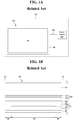
- FIG. 1A is a block diagram illustrating an electronic device 120 including an organic light emitting diode (OLED) device 100 and a signal source 104.
- the signal source 104 generates and sends electrical signals to the OLED device 100 via a signal line 108.
- the signal source 104 may be embodied as an integrated circuit (IC) for processing electronic signals.
- the electric signals are received at non-display area NA of the OLED device 100.
- the signals received at the non-display area NA of the OLED device 100 are processed and forwarded directly or forwarded directly without further processing to display area AA of the OLED device 100.
- the electronic device 120 may include, but is not limited to mobile electronic devices such as smartphones.
- FIG. 1B is a cross sectional view of an example organic light emitting diode (OLED) device 100.
- the OLED device 100 may include, for example, an organic light emitting layer FL, a back panel BP below the organic light emitting layer FL, a polarization film POL on the organic light emitting layer FL, a film type touch panel (or “touch film” or “touch panel film”) TSP placed over the polarization film POL, and a cover plate CV placed on the touch panel film TSP.
- OLED organic light emitting diode
- the back panel BP affords rigidity and strength to the OLED device 100.
- the back panel BP may also include traces or conductive lines for transmitting signals to or from the signal line 108. It is to be noted that the back panel BP is not necessarily placed at the "back" side of an OLED device, as described below in detail with reference to FIGS. 7 through 13 .
- the back panel (or "back plate”) may, for example, be surrounded by other components of the OLED device. To decrease the overall thickness of the OLED device 100, it is advantageous to use a thin back panel BP.
- the organic light emitting layer FL is used for generating images by operating OLEDs formed in pixel regions of the layer FL.
- the organic light emitting layer FL may include, among other components, a substrate and a plurality of layers (e.g., an emissive layer (EML), and electrodes) formed on the substrate.
- FIG. 1B illustrates an organic light emitting layer FL including a flexible base layer (substrate), a display element layer ACT, and a protecting layer BA attached onto the display element layer ACT by an adhesive layer ADH for protection.
- the display element layer ACT may be structured differently depending on the type of OLED implemented.
- the display element layer ACT may be implemented as a single layer device that typically includes an anode layer, an EML and a cathode layer formed on the substrate (i.e., a base layer).
- the display element layer ACT may be implemented as a triple-layer bottom-emitting OLED that typically includes an anode layer, a hole transport layer (HTL), an emissive layer (EML), an electron transport layer (ETL) and cathode layers formed on a substrate (i.e., a base layer).
- the base layer may be as thin as 0.5 mm.
- the organic light emitting layer FL is divided into a display area AA and a non-display area NA surrounding the display area AA.
- the display area AA refers to an area of the organic light emitting layer FL formed with thin film transistors (TFTs) and OLEDs. Based on the signals transmitted via the non-display area NA, the display area AA generates images on its surface by operating the TFTs and OLEDs.
- the non-display area NA refers to the remaining area of the organic light emitting layer FL including components (e.g., wires and circuits) for receiving signals for operating TFTs and OLEDs in the display area AA.
- Additional film elements for supporting the display function may be formed on the organic light emitting layer FL.
- a polarization film POL may be provided to prevent reflected surrounding light from interfering with the generated display images.
- a film type touch panel TSP for receiving user input may be attached to the organic light emitting layer FL.
- the touch film TSP may include a first touch film TS1 having a conductive line layer and a second touch film TS2 having a conductive line layer stacked on the organic light emitting layer FL, as illustrated in FIG. 1B .
- the first touch panel film TS1 for example the conductive line layer of the first touch panel film TS1, may include first touch electrode lines and the second touch panel film TS2, for example the conductive line layer of the second touch panel film TS2, may include second touch electrode lines.
- the first touch electrode lines may extend along a first direction and the second touch electrode lines may extend along a second direction different from the first direction.
- the second direction may be perpendicular to the first direction.
- the film type touch panel TSP may also include an area corresponding to a display area AA of the organic light emitting layer FL to transmit signals associated with the user's touch, and a remaining portion of the touch panel film TSP corresponding to non-display area NA for processing the signals.
- a cover plate CV may be placed to protect other elements disposed between the cover plate CV and the back panel BP.
- the OLED device 100 may be installed in the electronic device. As illustrated in FIG. 1B , portions of the frame FR may partially cover the top side portions of the OLED device 100.
- the top side portions of the OLED device 100 are often referred to as a bezel area where circuits or wires for operating the pixels in the organic light emitting layer FL are placed.
- the bezel area may include, among others, the non-display area NA of the organic light emitting layer FL.
- Embodiments and comparative examples described herein use flexible characteristics of OLED devices to form a non-display area NA in a plane separated from or forming an angle with respect to another plane along which a top flat area of the organic light emitting layer FL extends.
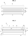
- FIG. 2 is a cross sectional view illustrating a structure of a thin OLED device 200 having an add-on type touch film TSP, according to one comparative example.
- FIG. 3 is a cross sectional view illustrating some components of the thin OLED device 200 bent downwards to reduce its bezel width, according to one comparative example.
- the OLED device 200 has substantially the same components as the OLED device 100, as described above with reference to FIG. 1 .
- the OLED device 200 is different from the OLED device 100 in that the touch panel film TSP and the organic light emitting layer FL extend beyond the polarization film POL and the back panel BP at both sides.
- the cover plate CV has curved sides CS that are curved downwards from a flat portion, e.g. a top portion, TS of the cover plate CV.
- the flat portion (e.g. top portion) TS and the curved sides CS define an interior 322 for accommodating other components of the OLED device 200.
- the non-display area NA of the organic light emitting layer FL and both sides of the touch panel film TSP extending beyond other components are bent downward as illustrated in FIG. 3 .
- the display area AA of the organic light emitting layer FL extends along plane 302.
- the non-display areas NA of the organic light emitting layer FL at both sides of the display area AA are bent vertically and extend along planes 306, 310, respectively.
- at least one (e.g., both) of planes 306, 310 may be perpendicular to plane 302.
- a flat portion (e.g. top portion) of the touch panel film TSP extends along plane 326 whereas the sides of the touch panel film TSP extend along planes 314, 316.
- plane 326 may be parallel or substantially parallel to plane 302.
- at least one (e.g., both) of planes 314, 316 may be parallel or substantially parallel to at least one (e.g., both) of planes 306, 310.
- at least one (e.g., both) of planes 314, 316 may be perpendicular to plane 326.
- the combined thickness of the first touch film TS1 and the second touch film TS2 is 0.1 mm, and hence, the minimum bending radius of the touch panel film TSP is 0.5 to 5 mm.
- the minimum width Wb of the bezel area at one side of the OLED device 200 corresponds to the sum of the minimum bending radius of the touch panel film TSP (at the outer top surface) and the thickness of the cover plate CV at the curved sides CS.
- the non-display area NA of the organic light emitting layer FL and the touch panel film TSP can be bent downward with the bezel width of 1 to 10 mm from the edge of the back panel BP.
- the non-display area NA of the organic light emitting layer FL and the touch panel film TSP may be bent downward without being affected by the adhesive layer.
- FIG. 4 is a cross sectional view illustrating a thin OLED device 400 having an on-cell type touch film TSL according to one comparative example.
- the thin OLED device 400 is substantially the same as the thin OLED device 200 except that the on-cell type touch film (or "touch screen layer” or “touch layer”) TSL is formed on the organic light emitting layer FL (and hence, referred to as on-cell type touch film TSL).
- the touch layer TSL may include a first touch layer having a conductive line layer extending in a first direction, and a second touch layer having a conductive line layer extending in a second direction different from the first direction.
- the first touch layer for example the conductive line layer of the first touch layer
- the second touch layer for example the conductive line layer of the second touch layer
- the first touch electrode lines may extend along the first direction
- the second touch electrode lines may extend along the second direction.
- the second direction may be perpendicular to the first direction.
- the touch layer TSL is formed directly on the organic light emitting layer FL
- a separate touch film TSP of the OLED device 200 may be obviated.
- the thickness of the organic light emitting layer FL having the touch layer TSL of the OLED device 400 may be substantially the same as the thickness of the OLED device 200. Assuming that the thickness of the organic light emitting layer FL is 1 mm, the minimum bending radius of 2.5 to 5 mm can be obtained according to equation (1).
- FIG. 5 is a cross sectional view illustrating an assembled version of the OLED device 400 of FIG. 4 , according to one comparative example.
- the organic light emitting layer FL has a top portion that extends along plane 502, a side portion extending along plane 506 and another side portion extending along plane 510.
- the plane 502 forms 90 degree angle with respect to the planes 506 and 510.
- the OLED device 400 does not have a separate touch panel film TSP (as in the case of the OLED device 200).
- the minimum width Wb 2 of the bezel area at one side of the OLED device 400 corresponds to the sum of the minimum bending radius of the organic light emitting layer FL (at the outer top surface) and the thickness of the cover plate CV at the curved sides CS.
- An adhesive layer for attaching the polarization film POL on the organic light emitting layer FL having the touch layer TSL or for attaching the cover plate CV to the polarization film POL may be added to securely bond the components.
- the adhesive layer is disposed to secure areas of the components covering only the display area AA. In this way, the non-display area NA of the organic light emitting layer FL (with the touch layer TSL) can be bent downward as illustrated in FIG. 5 .
- the OLED device 400 of FIG. 5 further includes a frame FR forming the bottom casing.
- the size of the frame FR may have the same length and width as the cover plate CV so that the edge surfaces of the curved sides CS of the cover plate CV can be attached to the upper surface of the frame FR.
- only the curved side portions CS of the cover plate CV and part of the non-display area NA corresponding to the bezel width Wd 2 are visible to the user from the front.
- FIG. 6 is a cross sectional view illustrating an OLED device without a back panel, according to one comparative example.
- the OLED device 600 of in FIG. 6 does not include any back panel. Instead, the organic light emitting layer FL (with the touch layer TSL) can be secured to the polarization film POL, which is in turn secured to the cover plate CV.
- the structure of the OLED device 600 is substantially the same as the OLED device 400. Even though the back panel is removed, the bent non-display NA area can be closely in contact with the inner surface of the curved side portions CS of the cover plate CV because the organic light emitting layer FL and/or the touch layer TSL are sufficiently elastic.
- a flat cover plate may be used in conjunction with a frame, as illustrated in FIG. 1B .
- the flat cover plate in such comparative example may be placed on top of a touch panel film TSP or an organic light emitting layer FL that extends beyond the flat cover plate.
- the frame securely clamps both sides of the touch panel film TSP, the organic light emitting layer FL and the flat cover plate.
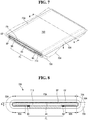
- FIG. 7 is a perspective view of an OLED device 700 with a display area AA extending across an upper surface and lateral sides of an electronic device, according to one comparative example.
- the OLED device 700 may include, among other components, a back panel (or "back plate") BP, the organic light emitting layer FL placed on the back panel BP, a frame FR and a cover plate CV.
- the cover plate CV is placed on the organic light emitting layer FL to cover at least the display area AA of the organic light emitting layer FL.
- the frame FR may form a part of the bottom of the OLED device 700.
- a cavity 718 may be formed in the middle of the back plate BP to house other components of the electronic device such as circuits (not shown).
- the OLED device 700 has a display area AA that extends not only across the upper part of the OLED device 700 but also across the side and bottom parts of the OLED device 700. In this way, images can be displayed not only through the top surface of the OLED device 700 but also through side surfaces and a part of the bottom surface of the OLED device 700.
- FIG. 8 is a cross-sectional view of the OLED device 700 taken along line M-N of FIG. 7 , according to one comparative example.
- the display area AA of the organic light emitting layer FL consists of an upper flat area FDA extending along plane 704, lower display areas BDA extending along plane 708 and side display areas SDA connecting the upper flat area FDA and the lower display areas BDA.
- the plane 708 is parallel to the plane 704 and is separated by distance d e .
- the distance d e may correspond to twice a bending radius of the organic light emitting layer FL.
- the distance d e may be twice the minimum bending radius of the organic light emitting layer FL.
- the organic light emitting layer FL is flexible, and hence, can be bent to embody the upper flat area FDA, the side display areas SDA, and the lower display areas BDA. Specifically, the side display areas SDA are bent 180 degrees, and connect the upper flat area FDA and the lower display areas BDA. Then bent organic light emitting layer FL can be secured to the back plate BP and/or to the cover plate CV to maintain its configuration.
- Non-display areas NA of the organic light emitting layer FL extend from the lower display areas BDA along the plane 708, as illustrated in FIG. 8 .
- Non-display areas NA of the organic light emitting layer FL may then be connected to wires or circuits to provide signals to the display area AA of the organic light emitting layer FL. Because the top surface of the OLED device 700 does not include the non-display areas NA, no bezel is visible to the user from the front of the OLED device 700.
- the display area AA may include only upper flat area FDA and side display areas SDA but not lower display areas BDA.
- the non-display areas NA of the organic light emitting layer FL may extend inwards from the side display areas SDA along the plane 708.
- only one side of the OLED device may have a side display area SDA but not the other side of the OLED device.
- the non-display area may be bent vertically downwards for connection to wires of circuits to embody a bezel-less display device.
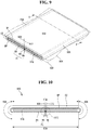
- FIG. 9 is a perspective view of an OLED device 900 with a display area AA extending across an entire upper surface, lateral sides and a substantially entire bottom surface, according to one embodiment.
- the OLED device 900 may include, among other components, a back panel BP, the organic light emitting layer FL placed on the back panel (or "back plate") BP, and a cover plate CV.
- the cover plate CV is placed on the organic light emitting layer to cover the entire output surface of the organic light emitting layer FL, which forms the display area AA.
- a cavity 916 may be formed in the middle of the back plate BP to house other components of the electronic device such as circuits (not shown).
- the OLED device 900 has a display area AA that extends not only across the upper part of the OLED device 900 but also across the entire side and bottom parts of the OLED device 900. In this way, images can be displayed not only through the top surface of the OLED device 900 but also through side surfaces and the bottom surface of the OLED device 900.
- the OLED device 900 may constitute an outer casing of a mobile device or other electronic devices.
- FIG. 10 is a cross-sectional view of the OLED device 900 taken along line O-P of FIG. 9 , according to one embodiment.
- the display area AA of the organic light emitting layer FL consists of an upper flat area FDA extending along plane 904, lower display areas BDA extending along plane 920 and side display areas SDA connecting the upper flat area FDA and the lower display areas BDA.
- the organic light emitting layer FL is flexible, and hence, can be bent to embody the upper flat area FDA, the side display areas SDA, and the lower display areas BDA. Then bent organic light emitting layer FL can be secured to the back plate BP and/or to the cover plate CV to maintain its configuration.
- FIG. 11 is an enlarged view of a section 1012 of the OLED device 900 in FIG. 10 , according to one embodiment.
- the non-display areas NA extending from the lower display areas BDA are bent upwards at the middle of the OLED device 900.
- One non-display area NA extends vertically along plane 908 while the other non-display area NA extends vertically along plane 912.
- planes 908 and 912 may be parallel or substantially parallel to one another.
- at least one (e.g. both) of planes 908 and 912 may be perpendicular or substantially perpendicular to plane 920 and/or plane 904.
- the minimum bending radius of the organic light emitting layer FL causes a small bezel of width W d3 to be present in middle region where the non-display areas NA meet.
- the width W d3 may be equal to twice the minimum bending radius of the organic light emitting layer FL.
- the non-display areas NA meet (and hence form a bezel area) at the bottom center of the OLED device 900.
- the two non-display areas NA may meet at locations other than the middle of the OLED device 900. That is, the non-display areas NA may meet at a location shifted to the left or right side from the middle portion as shown in FIG. 10 .
- the plane along which the non-display area of the organic light emitting layer FL extends may be set to be different from a plane along which an upper display area (e.g. upper flat area FDA) of the organic light emitting layer FL extends.
- an upper display area e.g. upper flat area FDA
- the width of bezel area can be reduced or be virtually eliminated to increase the display area of the OLED device.
Landscapes
- Engineering & Computer Science (AREA)
- Theoretical Computer Science (AREA)
- Physics & Mathematics (AREA)
- Computer Hardware Design (AREA)
- General Physics & Mathematics (AREA)
- Human Computer Interaction (AREA)
- General Engineering & Computer Science (AREA)
- Optics & Photonics (AREA)
- Signal Processing (AREA)
- Nonlinear Science (AREA)
- Microelectronics & Electronic Packaging (AREA)
- Mathematical Physics (AREA)
- Chemical & Material Sciences (AREA)
- Crystallography & Structural Chemistry (AREA)
- Electroluminescent Light Sources (AREA)
- Devices For Indicating Variable Information By Combining Individual Elements (AREA)
Description
- This application claims the benefit of Korean Patent Application with the publication number
KR 20140061934 A filed on November 14, 2012 - The present disclosure relates to a display panel with a bezel area of a reduced width. Especially, the present disclosure relates to a display panel having a non-display area extending along a plane different from a plane along which a flat display area extends.
- Nowadays, various flat panel display devices are available to overcome many drawbacks of the cathode ray tube such as heavy weight and bulk volume. The flat panel display devices include the liquid crystal display device (or LCD), the field emission display (or FED), the plasma display panel (or PDP) and the electroluminescence device (or EL).
- With light weight and thin thickness, the panel type display can be applied to display images for mobile communication devices and/or portable/personal information devices. Nowadays, for the portable or mobile applications, the requirement for the thinner, lighter and having lower power consumption display panel is ever increasing.
- An inorganic light emitting diode display device is a type of an electroluminescence display device. As a self-emitting display device, the electroluminescence display device has the advantages of a higher response speed, higher brightness and a large viewing angle. The organic light emitting diode comprises the organic light emitting material layer, and the cathode and the anode which are facing each other with the organic light emitting material layer therebetween.
- The organic light emitting diode display (or OLED) using the organic light emitting diode can be divided into two types: (i) the passive matrix type organic light emitting diode display (or PMOLED) and (ii) the active matrix type organic light emitting diode display (or AMOLED). Furthermore, the OLED may be divided into two types according to the direction of the emitted light: the top emission type and the bottom emission type.
- The organic light emitting diode display may be formed as a flexible display. The flexible active matrix type organic light emitting diode display (or Flexible AMOLED) shows the video data by controlling the current applying to the organic light emitting diode using the thin film transistor (or TFT).
-
US 2011/050657 A1 describes an electro-optical device, wherein a display panel has at least a display region V in which the plurality of pixels are formed and a frame region F formed outside the display region V, and wherein at least one side of each of the frame regions F is bent from the vicinity of a circumference of the display region V to the support frame side and is fixed to the support frame. -
US 2012/107978 A1 describes a method of fabricating a flexible display device, wherein a flexible substrate is easily detached from a carrier substrate without using a laser apparatus, and wherein deterioration such as lift of an organic electroluminescent diode and generation of a bubble is prevented. Therein, a second film may be a polarizing plate that selectively transmits a polarized light having a predetermined polarization axis and blocks the other light. -
EP 2 456 175 A1 describes an electronic device having a flexible display including a display area and a non-display or inactive area and a fold such that at least part of the non-display area is non-coplanar with the display area. -
EP 2 541 371 A2 -
EP 2065783 A1 describes a portable electronic apparatus having (at least) first and second display areas on a front side and a rear side of the apparatus' housing, respectively, an orientation sensor that provides an orientation sensor output signal, and a display controller which is responsive to the orientation sensor output signal to selectively control the first display area and the second display area. - Embodiments relate to a display device with a flexible display layer configured to reduce a size of a bezel area. The invention provides a display device according to
claim 1. Further embodiments of the invention are described in the dependent claims. - The accompanying drawings, which are included to provide a further understanding of the disclosure and are incorporated in and constitute a part of this specification, illustrate embodiments and together with the description serve to explain the principles of the embodiments.
-
FIG. 1A is a diagram illustrating an electronic device including an organic light emitting diode (OLED) device and a signal source. -
FIG. 1B is a cross sectional view illustrating the structure of an OLED device mounted using a frame. -
FIG. 2 is a cross sectional view illustrating a structure of a thin OLED device having an add-on type touch film, according to one comparative example. -
FIG. 3 is a cross sectional view illustrating components of the thin OLED device ofFIG. 2 bent downwards to reduce its bezel width, according to one comparative example. -
FIG. 4 is a cross sectional view illustrating a thin OLED device having an on-cell type touch film, according to one comparative example. -
FIG. 5 is a cross sectional view illustrating an assembled version of the OLED device ofFIG. 4 , according to one comparative example. -
FIG. 6 is a cross sectional view illustrating an OLED device without a back panel, according to one comparative example. -
FIG. 7 is a perspective view of an OLED device with a display area extending across an upper surface and lateral sides of an electronic device, according to one comparative example. -
FIG. 8 is a cross-sectional view of the OLED device taken along line M-N ofFIG. 7 , according to one comparative example. -
FIG. 9 is a perspective view of an OLED device with a display area extending across an entire upper surface, a substantially entire bottom surface and lateral sides, according to one embodiment. -
FIG. 10 is a cross-sectional view of the OLED device taken along line O-P ofFIG. 9 , according to one embodiment. -
FIG. 11 is an enlarged view of a section of the OLED device inFIG. 10 , according to one embodiment. - Embodiments of the present disclosure are described below with reference to Figures. Like reference numerals designate like elements throughout the detailed description. In the following embodiments, the names of the elements are selected for ease of explanation.
- Figure (
FIG.) 1A is a block diagram illustrating anelectronic device 120 including an organic light emitting diode (OLED)device 100 and asignal source 104. Thesignal source 104 generates and sends electrical signals to theOLED device 100 via asignal line 108. Thesignal source 104 may be embodied as an integrated circuit (IC) for processing electronic signals. - The electric signals are received at non-display area NA of the
OLED device 100. The signals received at the non-display area NA of theOLED device 100 are processed and forwarded directly or forwarded directly without further processing to display area AA of theOLED device 100. - The
electronic device 120 may include, but is not limited to mobile electronic devices such as smartphones. -
FIG. 1B is a cross sectional view of an example organic light emitting diode (OLED)device 100. TheOLED device 100 may include, for example, an organic light emitting layer FL, a back panel BP below the organic light emitting layer FL, a polarization film POL on the organic light emitting layer FL, a film type touch panel (or "touch film" or "touch panel film") TSP placed over the polarization film POL, and a cover plate CV placed on the touch panel film TSP. - The back panel BP affords rigidity and strength to the
OLED device 100. The back panel BP may also include traces or conductive lines for transmitting signals to or from thesignal line 108. It is to be noted that the back panel BP is not necessarily placed at the "back" side of an OLED device, as described below in detail with reference toFIGS. 7 through 13 . The back panel (or "back plate") may, for example, be surrounded by other components of the OLED device. To decrease the overall thickness of theOLED device 100, it is advantageous to use a thin back panel BP. - The organic light emitting layer FL is used for generating images by operating OLEDs formed in pixel regions of the layer FL. The organic light emitting layer FL may include, among other components, a substrate and a plurality of layers (e.g., an emissive layer (EML), and electrodes) formed on the substrate.
FIG. 1B illustrates an organic light emitting layer FL including a flexible base layer (substrate), a display element layer ACT, and a protecting layer BA attached onto the display element layer ACT by an adhesive layer ADH for protection. - The display element layer ACT may be structured differently depending on the type of OLED implemented. For example, the display element layer ACT may be implemented as a single layer device that typically includes an anode layer, an EML and a cathode layer formed on the substrate (i.e., a base layer). Alternatively, the display element layer ACT may be implemented as a triple-layer bottom-emitting OLED that typically includes an anode layer, a hole transport layer (HTL), an emissive layer (EML), an electron transport layer (ETL) and cathode layers formed on a substrate (i.e., a base layer). In order to decrease the thickness of the OLED device, the base layer may be as thin as 0.5 mm.
- The organic light emitting layer FL is divided into a display area AA and a non-display area NA surrounding the display area AA. The display area AA refers to an area of the organic light emitting layer FL formed with thin film transistors (TFTs) and OLEDs. Based on the signals transmitted via the non-display area NA, the display area AA generates images on its surface by operating the TFTs and OLEDs. The non-display area NA refers to the remaining area of the organic light emitting layer FL including components (e.g., wires and circuits) for receiving signals for operating TFTs and OLEDs in the display area AA.
- Additional film elements for supporting the display function may be formed on the organic light emitting layer FL. For example, a polarization film POL may be provided to prevent reflected surrounding light from interfering with the generated display images. As another example, a film type touch panel TSP for receiving user input may be attached to the organic light emitting layer FL. The touch film TSP may include a first touch film TS1 having a conductive line layer and a second touch film TS2 having a conductive line layer stacked on the organic light emitting layer FL, as illustrated in
FIG. 1B . The first touch panel film TS1, for example the conductive line layer of the first touch panel film TS1, may include first touch electrode lines and the second touch panel film TS2, for example the conductive line layer of the second touch panel film TS2, may include second touch electrode lines. The first touch electrode lines may extend along a first direction and the second touch electrode lines may extend along a second direction different from the first direction. The second direction may be perpendicular to the first direction. The film type touch panel TSP may also include an area corresponding to a display area AA of the organic light emitting layer FL to transmit signals associated with the user's touch, and a remaining portion of the touch panel film TSP corresponding to non-display area NA for processing the signals. - Furthermore, at the top of the
OLED device 100, a cover plate CV may be placed to protect other elements disposed between the cover plate CV and the back panel BP. Using a frame FR, for example, theOLED device 100 may be installed in the electronic device. As illustrated inFIG. 1B , portions of the frame FR may partially cover the top side portions of theOLED device 100. The top side portions of theOLED device 100 are often referred to as a bezel area where circuits or wires for operating the pixels in the organic light emitting layer FL are placed. The bezel area may include, among others, the non-display area NA of the organic light emitting layer FL. - In order to provide a larger display area on the same limited surface, it is advantageous to reduce the size of the bezel area. Especially, on mobile electronic devices, the increase in a display area of the OLED device by reducing the bezel area becomes more prominent. Embodiments and comparative examples described herein use flexible characteristics of OLED devices to form a non-display area NA in a plane separated from or forming an angle with respect to another plane along which a top flat area of the organic light emitting layer FL extends.
-
FIG. 2 is a cross sectional view illustrating a structure of athin OLED device 200 having an add-on type touch film TSP, according to one comparative example.FIG. 3 is a cross sectional view illustrating some components of thethin OLED device 200 bent downwards to reduce its bezel width, according to one comparative example. - The
OLED device 200 has substantially the same components as theOLED device 100, as described above with reference toFIG. 1 . TheOLED device 200 is different from theOLED device 100 in that the touch panel film TSP and the organic light emitting layer FL extend beyond the polarization film POL and the back panel BP at both sides. Furthermore, the cover plate CV has curved sides CS that are curved downwards from a flat portion, e.g. a top portion, TS of the cover plate CV. - The flat portion (e.g. top portion) TS and the curved sides CS define an interior 322 for accommodating other components of the
OLED device 200. - The non-display area NA of the organic light emitting layer FL and both sides of the touch panel film TSP extending beyond other components are bent downward as illustrated in
FIG. 3 . The display area AA of the organic light emitting layer FL extends alongplane 302. The non-display areas NA of the organic light emitting layer FL at both sides of the display area AA are bent vertically and extend alongplanes planes plane 302. Similarly, a flat portion (e.g. top portion) of the touch panel film TSP extends alongplane 326 whereas the sides of the touch panel film TSP extend alongplanes plane 326 may be parallel or substantially parallel toplane 302. In one or more comparative examples, at least one (e.g., both) ofplanes planes planes plane 326. - The minimum bending radius (or "minimum radius of curvature") that a thin film may take without damage due to bending can be expressed in the following equation:

OLED device 200 corresponds to the sum of the minimum bending radius of the touch panel film TSP (at the outer top surface) and the thickness of the cover plate CV at the curved sides CS. - Therefore, the non-display area NA of the organic light emitting layer FL and the touch panel film TSP can be bent downward with the bezel width of 1 to 10 mm from the edge of the back panel BP. Especially, by forming an adhesive layer for attaching the cover plate CV with the touch film TSP and another adhesive layer for attaching the touch film TSP with the polarization film POL only on the display area AA of the organic light emitting layer FL, the non-display area NA of the organic light emitting layer FL and the touch panel film TSP may be bent downward without being affected by the adhesive layer.
Furthermore, by attaching the end surface of the curved side portions CS of the cover plate CV with the frame (not shown in figures), only the curved side portions CS of the cover plate CV are externally visible to a user from the front of the panel. Therefore, virtually no bezel area is visible to the user, and the so-called bezel-less or non-bezel display can be achieved. -
FIG. 4 is a cross sectional view illustrating athin OLED device 400 having an on-cell type touch film TSL according to one comparative example. Thethin OLED device 400 is substantially the same as thethin OLED device 200 except that the on-cell type touch film (or "touch screen layer" or "touch layer") TSL is formed on the organic light emitting layer FL (and hence, referred to as on-cell type touch film TSL). The touch layer TSL may include a first touch layer having a conductive line layer extending in a first direction, and a second touch layer having a conductive line layer extending in a second direction different from the first direction. In one or more comparative examples, the first touch layer, for example the conductive line layer of the first touch layer, may include first touch electrode lines, and the second touch layer, for example the conductive line layer of the second touch layer, may include second touch electrode lines. In one or more comparative examples, the first touch electrode lines may extend along the first direction and the second touch electrode lines may extend along the second direction. In one or more comparative examples, the second direction may be perpendicular to the first direction. - As the touch layer TSL is formed directly on the organic light emitting layer FL, a separate touch film TSP of the
OLED device 200 may be obviated. The thickness of the organic light emitting layer FL having the touch layer TSL of theOLED device 400 may be substantially the same as the thickness of theOLED device 200. Assuming that the thickness of the organic light emitting layer FL is 1 mm, the minimum bending radius of 2.5 to 5 mm can be obtained according to equation (1). -
FIG. 5 is a cross sectional view illustrating an assembled version of theOLED device 400 ofFIG. 4 , according to one comparative example. As illustrated inFIG. 5 , the organic light emitting layer FL has a top portion that extends alongplane 502, a side portion extending alongplane 506 and another side portion extending alongplane 510. In the comparative example ofFIG. 5 , theplane 502 forms 90 degree angle with respect to theplanes - The
OLED device 400 does not have a separate touch panel film TSP (as in the case of the OLED device 200). The minimum width Wb2 of the bezel area at one side of theOLED device 400 corresponds to the sum of the minimum bending radius of the organic light emitting layer FL (at the outer top surface) and the thickness of the cover plate CV at the curved sides CS. - An adhesive layer for attaching the polarization film POL on the organic light emitting layer FL having the touch layer TSL or for attaching the cover plate CV to the polarization film POL may be added to securely bond the components. In one comparative example, the adhesive layer is disposed to secure areas of the components covering only the display area AA. In this way, the non-display area NA of the organic light emitting layer FL (with the touch layer TSL) can be bent downward as illustrated in
FIG. 5 . - The
OLED device 400 ofFIG. 5 further includes a frame FR forming the bottom casing. The size of the frame FR may have the same length and width as the cover plate CV so that the edge surfaces of the curved sides CS of the cover plate CV can be attached to the upper surface of the frame FR. In such structure, only the curved side portions CS of the cover plate CV and part of the non-display area NA corresponding to the bezel width Wd2 are visible to the user from the front. -
FIG. 6 is a cross sectional view illustrating an OLED device without a back panel, according to one comparative example. TheOLED device 600 of inFIG. 6 does not include any back panel. Instead, the organic light emitting layer FL (with the touch layer TSL) can be secured to the polarization film POL, which is in turn secured to the cover plate CV. Other than obviating the back panel, the structure of theOLED device 600 is substantially the same as theOLED device 400. Even though the back panel is removed, the bent non-display NA area can be closely in contact with the inner surface of the curved side portions CS of the cover plate CV because the organic light emitting layer FL and/or the touch layer TSL are sufficiently elastic. - In other comparative examples, instead of using a cover plate with curved sides as described above with reference to
FIGS. 2-6 , a flat cover plate may be used in conjunction with a frame, as illustrated inFIG. 1B . The flat cover plate in such comparative example may be placed on top of a touch panel film TSP or an organic light emitting layer FL that extends beyond the flat cover plate. The frame securely clamps both sides of the touch panel film TSP, the organic light emitting layer FL and the flat cover plate. -
FIG. 7 is a perspective view of anOLED device 700 with a display area AA extending across an upper surface and lateral sides of an electronic device, according to one comparative example. TheOLED device 700 may include, among other components, a back panel (or "back plate") BP, the organic light emitting layer FL placed on the back panel BP, a frame FR and a cover plate CV. The cover plate CV is placed on the organic light emitting layer FL to cover at least the display area AA of the organic light emitting layer FL. The frame FR may form a part of the bottom of theOLED device 700. Acavity 718 may be formed in the middle of the back plate BP to house other components of the electronic device such as circuits (not shown). - The
OLED device 700 has a display area AA that extends not only across the upper part of theOLED device 700 but also across the side and bottom parts of theOLED device 700. In this way, images can be displayed not only through the top surface of theOLED device 700 but also through side surfaces and a part of the bottom surface of theOLED device 700. -
FIG. 8 is a cross-sectional view of theOLED device 700 taken along line M-N ofFIG. 7 , according to one comparative example. The display area AA of the organic light emitting layer FL consists of an upper flat area FDA extending alongplane 704, lower display areas BDA extending alongplane 708 and side display areas SDA connecting the upper flat area FDA and the lower display areas BDA. Theplane 708 is parallel to theplane 704 and is separated by distance de. In one or more comparative examples, the distance de may correspond to twice a bending radius of the organic light emitting layer FL. For example, in one or more comparative examples, the distance de may be twice the minimum bending radius of the organic light emitting layer FL. The organic light emitting layer FL is flexible, and hence, can be bent to embody the upper flat area FDA, the side display areas SDA, and the lower display areas BDA. Specifically, the side display areas SDA are bent 180 degrees, and connect the upper flat area FDA and the lower display areas BDA. Then bent organic light emitting layer FL can be secured to the back plate BP and/or to the cover plate CV to maintain its configuration. - Non-display areas NA of the organic light emitting layer FL extend from the lower display areas BDA along the
plane 708, as illustrated inFIG. 8 . Non-display areas NA of the organic light emitting layer FL may then be connected to wires or circuits to provide signals to the display area AA of the organic light emitting layer FL. Because the top surface of theOLED device 700 does not include the non-display areas NA, no bezel is visible to the user from the front of theOLED device 700. - Although the
OLED device 700 ofFIGS. 7 and 8 include the lower display areas BDA, in other comparative examples, the display area AA may include only upper flat area FDA and side display areas SDA but not lower display areas BDA. In such comparative examples, the non-display areas NA of the organic light emitting layer FL may extend inwards from the side display areas SDA along theplane 708. Also, in yet other comparative examples, only one side of the OLED device may have a side display area SDA but not the other side of the OLED device. On the side without the side display area SDA, the non-display area may be bent vertically downwards for connection to wires of circuits to embody a bezel-less display device. -
FIG. 9 is a perspective view of anOLED device 900 with a display area AA extending across an entire upper surface, lateral sides and a substantially entire bottom surface, according to one embodiment. TheOLED device 900 may include, among other components, a back panel BP, the organic light emitting layer FL placed on the back panel (or "back plate") BP, and a cover plate CV. The cover plate CV is placed on the organic light emitting layer to cover the entire output surface of the organic light emitting layer FL, which forms the display area AA. Acavity 916 may be formed in the middle of the back plate BP to house other components of the electronic device such as circuits (not shown). - The
OLED device 900 has a display area AA that extends not only across the upper part of theOLED device 900 but also across the entire side and bottom parts of theOLED device 900. In this way, images can be displayed not only through the top surface of theOLED device 900 but also through side surfaces and the bottom surface of theOLED device 900. TheOLED device 900 may constitute an outer casing of a mobile device or other electronic devices. -
FIG. 10 is a cross-sectional view of theOLED device 900 taken along line O-P ofFIG. 9 , according to one embodiment. The display area AA of the organic light emitting layer FL consists of an upper flat area FDA extending alongplane 904, lower display areas BDA extending alongplane 920 and side display areas SDA connecting the upper flat area FDA and the lower display areas BDA. The organic light emitting layer FL is flexible, and hence, can be bent to embody the upper flat area FDA, the side display areas SDA, and the lower display areas BDA. Then bent organic light emitting layer FL can be secured to the back plate BP and/or to the cover plate CV to maintain its configuration. -
FIG. 11 is an enlarged view of asection 1012 of theOLED device 900 inFIG. 10 , according to one embodiment. As shown inFIG. 11 , the non-display areas NA extending from the lower display areas BDA are bent upwards at the middle of theOLED device 900. One non-display area NA extends vertically alongplane 908 while the other non-display area NA extends vertically alongplane 912. In one or more embodiments,planes planes plane 904. The minimum bending radius of the organic light emitting layer FL causes a small bezel of width Wd3 to be present in middle region where the non-display areas NA meet. For example, in one or more embodiments, the width Wd3 may be equal to twice the minimum bending radius of the organic light emitting layer FL. - In the
OLED device 900, the non-display areas NA meet (and hence form a bezel area) at the bottom center of theOLED device 900. In other embodiments, the two non-display areas NA may meet at locations other than the middle of theOLED device 900. That is, the non-display areas NA may meet at a location shifted to the left or right side from the middle portion as shown inFIG. 10 . - By taking advantage of the flexible properties of the organic light emitting layer FL, the plane along which the non-display area of the organic light emitting layer FL extends may be set to be different from a plane along which an upper display area (e.g. upper flat area FDA) of the organic light emitting layer FL extends. In this way, the width of bezel area can be reduced or be virtually eliminated to increase the display area of the OLED device.
Claims (9)
- A display device comprising:
a flexible display layer (FL), the flexible display layer (FL) comprising:
a display area (AA) comprising:an upper flat area (FDA) extending along a first plane (904);lower display areas (BDA) extending along a second plane (920), which is parallel to the first plane (904) and separated from the first plane (904) by a distance (de); andbent side display areas (SDA) connecting the upper flat area (FDA) and the lower display areas (BDA); and non-display areas (NA) extending from at least one edge of the lower display areas (BDA) at a location where the lower display areas (BDA) meet, wherein the non-display areas (NA) are bent to extend towards the first plane (904), and configured to receive a signal for displaying an image on the flexible display layer (FL), wherein the display area (AA) extends across an entire upper surface, lateral sides, and the bottom surface of the display device. - The display device of claim 1, further comprising:a transparent cover plate (CV) comprising a flat portion;wherein the flexible display layer (FL) is secured to the transparent cover plate (CV),wherein the upper flat area extends along the first plane below the flat portion of the transparent cover plate (CV).
- The display device of claim 2, wherein the transparent cover plate (CV) comprises side portions extending from edges of the flat portion, the side portions of the transparent cover plate (CV) in conjunction with the flat portion of the transparent cover plate (CV) defining space for holding the flexible display layer (FL).
- The display device of claims 2 or 3, further comprising a touch panel layer between the transparent cover plate (CV) and the flexible display layer (FL), the touch panel layer coextensive with the flexible display layer (FL),
- The display device of claim 4, wherein the touch panel layer comprises:a first touch panel sub-layer having first touch electrode lines; anda second touch panel sub-layer having second touch electrode lines.
- The display device of any one of claims 2 to 5, further comprising a polarization film (POL) between the transparent cover plate (CV) and the flexible display layer (FL), the polarization film (POL) coextensive with the display area (AA) of the flexible display layer (FL).
- The display device of claim 6, wherein the polarization film (POL) is secured to the display area (AA) of the flexible display layer (FL) but not to the non-display areas (NA) of the flexible display layer (FL).
- The display device of any one of claims 1 to 7, wherein the flexible display layer (FL) comprises an organic light emitting layer.
- The display device of any one of claims 1 to 8,
wherein the at least one side display area (SDA) is bent by 180 degrees.
Applications Claiming Priority (1)
| Application Number | Priority Date | Filing Date | Title |
|---|---|---|---|
| KR1020120129152A KR101615791B1 (en) | 2012-11-14 | 2012-11-14 | None-Bezel Display Panel Having Edge Bending Structure |
Publications (2)
| Publication Number | Publication Date |
|---|---|
| EP2733912A1 EP2733912A1 (en) | 2014-05-21 |
| EP2733912B1 true EP2733912B1 (en) | 2019-10-09 |
Family
ID=49378146
Family Applications (1)
| Application Number | Title | Priority Date | Filing Date |
|---|---|---|---|
| EP13188854.7A Active EP2733912B1 (en) | 2012-11-14 | 2013-10-16 | Display device having bent non-display area for reduced bezel width |
Country Status (4)
| Country | Link |
|---|---|
| US (1) | US9697764B2 (en) |
| EP (1) | EP2733912B1 (en) |
| KR (1) | KR101615791B1 (en) |
| CN (1) | CN103810945B (en) |
Families Citing this family (106)
| Publication number | Priority date | Publication date | Assignee | Title |
|---|---|---|---|---|
| KR101515629B1 (en) * | 2012-01-07 | 2015-04-27 | 삼성전자주식회사 | Method and apparatus for providing event of portable device having flexible display unit |
| KR20140039845A (en) * | 2012-09-25 | 2014-04-02 | 삼성전기주식회사 | Touch panel and manufacturing method thereof |
| USD795854S1 (en) * | 2012-11-09 | 2017-08-29 | Samsung Display Co., Ltd. | Mobile phone |
| USD747301S1 (en) * | 2013-06-14 | 2016-01-12 | Lg Electronics Inc. | Mobile phone |
| KR102148428B1 (en) * | 2013-08-06 | 2020-08-27 | 삼성디스플레이 주식회사 | Display apparatus and electronic apparatus comprising the same |
| CN103513412B (en) * | 2013-09-16 | 2015-10-07 | 华为终端有限公司 | Periscope type lens and terminal device |
| JP6454482B2 (en) * | 2014-05-28 | 2019-01-16 | 京セラ株式会社 | Mobile device |
| KR102281910B1 (en) * | 2014-06-26 | 2021-07-28 | 삼성디스플레이 주식회사 | Display module and display apparatus having the same |
| KR102155252B1 (en) * | 2014-07-01 | 2020-09-11 | 엘지디스플레이 주식회사 | Organic light emitting display device and method of manufacturing the same |
| KR102397800B1 (en) * | 2014-07-25 | 2022-05-16 | 엘지디스플레이 주식회사 | Display Having Edge Bending Structure And Method For Manufacturing The Same |
| KR102353034B1 (en) * | 2014-08-11 | 2022-01-19 | 삼성디스플레이 주식회사 | Flexible orgainic light emitting diode |
| EP3174033A4 (en) * | 2014-09-02 | 2018-06-20 | Shenzhen Royole Technologies Co. Ltd. | Display module and electronic device having said display module |
| KR101921010B1 (en) * | 2014-09-02 | 2018-11-21 | 선전 로욜 테크놀로지스 컴퍼니 리미티드 | Display module and electronic device having said display module |
| CN107208854B (en) * | 2014-09-03 | 2020-06-05 | 乐金显示有限公司 | Multipurpose auxiliary lamp |
| CN104240607B (en) * | 2014-09-11 | 2017-07-04 | 合肥京东方光电科技有限公司 | Display device |
| KR102250710B1 (en) * | 2014-10-31 | 2021-05-10 | 엘지디스플레이 주식회사 | Organic light emitting display device and method of manufacturing the same |
| CN104460089B (en) * | 2014-12-12 | 2018-02-16 | 京东方科技集团股份有限公司 | A kind of Multiside displaying device part |
| CN104460088A (en) * | 2014-12-12 | 2015-03-25 | 京东方科技集团股份有限公司 | Multi-face display device |
| CN104409020B (en) | 2014-12-15 | 2017-09-15 | 京东方科技集团股份有限公司 | A kind of display panel and display device |
| KR102358750B1 (en) * | 2014-12-29 | 2022-02-07 | 엘지전자 주식회사 | The Apparatus and Method for Portable Device |
| KR102350858B1 (en) * | 2014-12-30 | 2022-01-12 | 엘지디스플레이 주식회사 | Display device including flexible substrate |
| US9287329B1 (en) * | 2014-12-30 | 2016-03-15 | Lg Display Co., Ltd. | Flexible display device with chamfered polarization layer |
| CN104639687B (en) * | 2015-01-30 | 2016-03-02 | 深圳市中兴移动通信有限公司 | Mobile terminal and display unit thereof |
| US10236459B2 (en) * | 2015-02-04 | 2019-03-19 | Sharp Kabushiki Kaisha | Display device and method for producing same |
| CN104637431B (en) * | 2015-02-05 | 2019-03-15 | 京东方科技集团股份有限公司 | GOA circuit and driving method, flexible display device and method for controlling display |
| JP6404150B2 (en) * | 2015-03-12 | 2018-10-10 | 株式会社ジャパンディスプレイ | Manufacturing method of display device |
| CN106157821A (en) * | 2015-04-03 | 2016-11-23 | 昆山工研院新型平板显示技术中心有限公司 | A kind of flexible display device |
| KR102410549B1 (en) | 2015-04-09 | 2022-06-20 | 삼성전자주식회사 | Electronic Device with Bezel-less Screen |
| KR102378361B1 (en) * | 2015-04-15 | 2022-03-25 | 삼성디스플레이 주식회사 | Flexible display device and method of manufacturing the same |
| KR20160124310A (en) * | 2015-04-16 | 2016-10-27 | 삼성디스플레이 주식회사 | Display module |
| CN104866019A (en) * | 2015-04-20 | 2015-08-26 | 广东欧珀移动通信有限公司 | Display components and terminals |
| KR102380158B1 (en) | 2015-04-24 | 2022-03-29 | 삼성디스플레이 주식회사 | Display device and manufacturing method thereof |
| CN104850183A (en) | 2015-05-21 | 2015-08-19 | 小米科技有限责任公司 | Mobile terminal display structure and mobile terminal |
| KR102348956B1 (en) | 2015-07-31 | 2022-01-10 | 엘지디스플레이 주식회사 | Multi vision display apparatus using a flexible display device |
| KR102288354B1 (en) * | 2015-08-10 | 2021-08-11 | 삼성디스플레이 주식회사 | Method for manufacturing flexible display apparatus |
| KR102550857B1 (en) * | 2015-08-13 | 2023-07-05 | 엘지디스플레이 주식회사 | Flexible display device |
| CN106502440A (en) * | 2015-09-08 | 2017-03-15 | 宸鸿科技(厦门)有限公司 | Touch control display apparatus and preparation method thereof |
| KR102444688B1 (en) * | 2015-09-18 | 2022-09-20 | 삼성디스플레이 주식회사 | Display device and manufacturing method thereof |
| KR102404370B1 (en) * | 2015-10-02 | 2022-06-03 | 삼성디스플레이 주식회사 | Window and display device having the same |
| CN105139767A (en) * | 2015-10-12 | 2015-12-09 | 昆山龙腾光电有限公司 | Display panel and display device |
| KR102382046B1 (en) * | 2015-11-04 | 2022-04-04 | 삼성디스플레이 주식회사 | Display device and portable terminal |
| USD838270S1 (en) * | 2015-11-06 | 2019-01-15 | Samsung Display Co., Ltd. | Display device |
| CN105892131A (en) * | 2016-06-23 | 2016-08-24 | 奥捷五金(江苏)有限公司 | Frame-free displayer and electronic equipment with same |
| KR102660537B1 (en) | 2016-07-19 | 2024-04-26 | 삼성디스플레이 주식회사 | Display apparatus |
| CN105976718B (en) * | 2016-07-20 | 2019-11-26 | 武汉华星光电技术有限公司 | Display panel and its display |
| USD837790S1 (en) * | 2016-08-03 | 2019-01-08 | Transcend Information, Inc. | Mobile storage device |
| CN106406443A (en) * | 2016-08-29 | 2017-02-15 | 珠海市魅族科技有限公司 | Cover board of intelligent terminal, cover board with touch function and touch display screen |
| EP3293606B1 (en) * | 2016-09-09 | 2020-12-30 | Samsung Display Co., Ltd. | Display device and method of manufacturing electronic device using the same |
| US20180090720A1 (en) * | 2016-09-27 | 2018-03-29 | Universal Display Corporation | Flexible OLED Display Module |
| KR101992916B1 (en) * | 2016-09-30 | 2019-06-25 | 엘지디스플레이 주식회사 | Organic light emitting display with touch sensor and fabricating method thereof |
| KR101992915B1 (en) * | 2016-09-30 | 2019-06-25 | 엘지디스플레이 주식회사 | Organic light emitting display with touch sensor and fabricating method thereof |
| KR102263379B1 (en) * | 2016-12-01 | 2021-06-11 | 주식회사 오성디스플레이 | Method for press molding of compound material |
| CN106783920B (en) * | 2016-12-21 | 2019-10-25 | 深圳市华星光电技术有限公司 | Flexible OLED-based display panel, seamless splicing display device and manufacturing method thereof |
| KR102612041B1 (en) | 2016-12-30 | 2023-12-07 | 엘지디스플레이 주식회사 | Foldable display device |
| JP6831710B2 (en) * | 2017-01-30 | 2021-02-17 | 株式会社ジャパンディスプレイ | Display device manufacturing method and display device |
| KR102388902B1 (en) | 2017-05-26 | 2022-04-22 | 삼성디스플레이 주식회사 | Display device and electronic device having the same |
| KR102333206B1 (en) * | 2017-07-07 | 2021-12-01 | 삼성디스플레이 주식회사 | Electronic apparatus |
| JP2019020448A (en) * | 2017-07-11 | 2019-02-07 | 株式会社ジャパンディスプレイ | Display device |
| CN107479752B (en) * | 2017-08-14 | 2020-06-05 | 业成科技(成都)有限公司 | Touch control display device |
| CN109428952A (en) * | 2017-08-21 | 2019-03-05 | 上海和辉光电有限公司 | A kind of mobile terminal of Rimless |
| KR102404974B1 (en) * | 2017-09-12 | 2022-06-03 | 삼성디스플레이 주식회사 | Display device |
| JP6407487B1 (en) | 2017-11-08 | 2018-10-17 | 堺ディスプレイプロダクト株式会社 | Display device and manufacturing method of display device |
| CN107886849A (en) * | 2017-11-28 | 2018-04-06 | 武汉华星光电半导体显示技术有限公司 | Abnormal curved surface display screen and preparation method thereof |
| KR102439590B1 (en) * | 2017-11-30 | 2022-09-01 | 엘지디스플레이 주식회사 | display device |
| CN107978623B (en) * | 2017-11-30 | 2021-02-19 | 武汉天马微电子有限公司 | Display device |
| KR102407746B1 (en) | 2017-12-01 | 2022-06-13 | 삼성전자주식회사 | Electronic device with full-display |
| KR102452529B1 (en) * | 2017-12-12 | 2022-10-11 | 삼성디스플레이 주식회사 | Flexible substrate and display device including the same |
| CN108010448B (en) * | 2017-12-20 | 2020-05-01 | 上海天马微电子有限公司 | Flexible display and display device |
| CN107948366B (en) * | 2017-12-29 | 2020-07-21 | Oppo广东移动通信有限公司 | Mobile terminal |
| CN107948365A (en) * | 2017-12-29 | 2018-04-20 | 广东欧珀移动通信有限公司 | Display module and mobile terminal |
| CN110085740B (en) | 2018-01-25 | 2022-01-11 | 绵阳京东方光电科技有限公司 | Flexible substrate, manufacturing method thereof, panel and electronic device |
| CN108172124B (en) * | 2018-01-26 | 2020-04-07 | 武汉华星光电技术有限公司 | Flexible display device |
| KR102522285B1 (en) * | 2018-03-05 | 2023-04-19 | 삼성디스플레이 주식회사 | Display device |
| KR102451750B1 (en) * | 2018-03-26 | 2022-10-06 | 삼성전자 주식회사 | Electronic device and method for forming flexible display of electronic device |
| CN108538211A (en) * | 2018-04-08 | 2018-09-14 | 深圳市华星光电半导体显示技术有限公司 | Oled display |
| CN110392142A (en) * | 2018-04-23 | 2019-10-29 | Oppo广东移动通信有限公司 | Electronic device, curved screen thereof and manufacturing method of curved screen |
| CN110401741B (en) * | 2018-04-25 | 2021-04-27 | Oppo广东移动通信有限公司 | an electronic device |
| CN108766241B (en) * | 2018-05-31 | 2021-10-15 | 广州国显科技有限公司 | Display panel, manufacturing method thereof and display device |
| JP6671420B2 (en) * | 2018-06-18 | 2020-03-25 | 堺ディスプレイプロダクト株式会社 | Display device and method of manufacturing display device |
| CN108877500B (en) * | 2018-06-29 | 2021-05-04 | 上海天马有机发光显示技术有限公司 | Display device and preparation method thereof |
| CN108803955A (en) * | 2018-07-04 | 2018-11-13 | 三星电子(中国)研发中心 | A kind of touch-control system |
| JP6613512B1 (en) * | 2018-08-31 | 2019-12-04 | レノボ・シンガポール・プライベート・リミテッド | Electronics |
| CN109256039B (en) * | 2018-10-18 | 2020-06-16 | 武汉华星光电半导体显示技术有限公司 | Display panel and electronic device |
| CN109215521B (en) * | 2018-10-23 | 2022-03-25 | 维沃移动通信有限公司 | Display module, electronic equipment and manufacturing method of display module |
| US11817025B1 (en) * | 2018-11-13 | 2023-11-14 | Apple Inc. | Electronic devices having housings with image transport layers |
| JP2020095146A (en) * | 2018-12-12 | 2020-06-18 | 株式会社デンソー | Display device |
| CN109920938B (en) * | 2019-03-26 | 2021-03-19 | 京东方科技集团股份有限公司 | OLED display panel and OLED display device |
| US11073869B2 (en) * | 2019-03-29 | 2021-07-27 | Samsung Electronics Co., Ltd. | Electronic device with coating for protection of window |
| CN110035155A (en) * | 2019-04-19 | 2019-07-19 | Oppo(重庆)智能科技有限公司 | A kind of terminal device |
| KR102068729B1 (en) * | 2019-04-26 | 2020-01-28 | (주)유티아이 | Flexible Cover Window |
| US11880235B2 (en) * | 2019-05-10 | 2024-01-23 | Apple Inc. | Electronic devices with enhanced display areas |
| KR102839811B1 (en) * | 2019-05-29 | 2025-07-30 | 삼성디스플레이 주식회사 | Display device |
| CN112289175B (en) * | 2019-07-24 | 2022-09-02 | 北京小米移动软件有限公司 | Display panel manufacturing method, display panel and terminal |
| CN112700728A (en) * | 2019-10-23 | 2021-04-23 | Oppo广东移动通信有限公司 | Display module and electronic equipment |
| TWI739561B (en) * | 2019-12-23 | 2021-09-11 | 仁寶電腦工業股份有限公司 | Electronic device |
| CN111136960A (en) * | 2019-12-27 | 2020-05-12 | 武汉华星光电半导体显示技术有限公司 | Cover plate and display device |
| TWI718841B (en) * | 2020-01-13 | 2021-02-11 | 恆顥科技股份有限公司 | Portable electronic apparatus with display and input functions |
| CN111292622B (en) * | 2020-02-26 | 2022-01-25 | 云谷(固安)科技有限公司 | Display panel and display device |
| US12035556B2 (en) | 2020-03-20 | 2024-07-09 | Chengdu Boe Optoelectronics Technology Co., Ltd. | Display device and method for manufacturing the same |
| US11335258B2 (en) | 2020-04-29 | 2022-05-17 | Dell Products L.P. | Information handling system thin display with minimal bezel |
| US11304317B2 (en) * | 2020-06-19 | 2022-04-12 | Motorola Mobility Llc | Unitary pre-formed fascia spanning at least two sides of an electronic device housing and corresponding methods and devices |
| CN111681539B (en) * | 2020-06-24 | 2022-03-29 | Oppo广东移动通信有限公司 | Display module, manufacturing method thereof and electronic equipment |
| CN112614429B (en) * | 2020-12-15 | 2022-07-29 | 合肥维信诺科技有限公司 | Display panel and display device |
| CN112732127B (en) * | 2020-12-30 | 2022-08-12 | 武汉天马微电子有限公司 | A display panel and display device |
| CN112928226A (en) * | 2021-01-28 | 2021-06-08 | 京东方科技集团股份有限公司 | Flexible display screen, forming process and gluing device for forming process |
| CN116897330A (en) | 2021-08-23 | 2023-10-17 | 京东方科技集团股份有限公司 | Touch substrate, display touch panel and display device |
Citations (1)
| Publication number | Priority date | Publication date | Assignee | Title |
|---|---|---|---|---|
| EP2065783A1 (en) * | 2007-11-30 | 2009-06-03 | Telefonaktiebolaget LM Ericsson (publ) | A portable electronic apparatus having more than one display area, and a method of controlling a user interface thereof |
Family Cites Families (22)
| Publication number | Priority date | Publication date | Assignee | Title |
|---|---|---|---|---|
| JP2003015542A (en) * | 2001-06-27 | 2003-01-17 | Toshiba Corp | Display device and liquid crystal display device |
| JP2003280542A (en) * | 2002-03-26 | 2003-10-02 | Seiko Epson Corp | Display module and electronic equipment |
| JP2003288022A (en) * | 2002-03-27 | 2003-10-10 | Matsushita Electric Ind Co Ltd | Liquid crystal display |
| JP4270137B2 (en) * | 2005-02-14 | 2009-05-27 | ソニー株式会社 | Display device |
| JP2007248689A (en) * | 2006-03-15 | 2007-09-27 | Hitachi Displays Ltd | Image display |
| TWI408628B (en) * | 2006-11-09 | 2013-09-11 | Creator Technology Bv | Secondary display integration in flexible display devices |
| US20110285607A1 (en) * | 2009-01-19 | 2011-11-24 | Si Hwan Kim | Portable display device |
| KR101577222B1 (en) | 2009-05-01 | 2015-12-15 | 엘지디스플레이 주식회사 | Organic electroluminescence display device including touch sensor and manufacturing method thereof |
| US8576209B2 (en) * | 2009-07-07 | 2013-11-05 | Semiconductor Energy Laboratory Co., Ltd. | Display device |
| CN101943965B (en) | 2009-07-08 | 2013-09-18 | 群康科技(深圳)有限公司 | Touch screen and electronic device therewith |
| JP5644075B2 (en) * | 2009-08-25 | 2014-12-24 | セイコーエプソン株式会社 | Electro-optical device and electronic apparatus |
| US8593061B2 (en) | 2009-08-25 | 2013-11-26 | Seiko Epson Corporation | Electro-optical device and electronic apparatus |
| KR101267529B1 (en) | 2010-10-30 | 2013-05-24 | 엘지디스플레이 주식회사 | Method of fabricating flexible organic electro luminescent device |
| EP2456175B1 (en) | 2010-11-19 | 2014-01-15 | BlackBerry Limited | Portable electronic device including flexible display |
| KR101739136B1 (en) | 2010-12-03 | 2017-05-23 | 엘지디스플레이 주식회사 | Method For Manufacturing An Organic Light Emitting Display Device And The Organic Light Emitting Display Device By The Same Method |
| KR20120091871A (en) | 2011-02-10 | 2012-08-20 | 삼성디스플레이 주식회사 | Display device and method for manufacturing the same |
| US10061356B2 (en) | 2011-06-30 | 2018-08-28 | Samsung Display Co., Ltd. | Flexible display panel and display apparatus including the flexible display panel |
| KR101320384B1 (en) * | 2011-06-30 | 2013-10-23 | 삼성디스플레이 주식회사 | Flexible display panel and the display apparatus comprising the flexible display panel |
| US8723824B2 (en) * | 2011-09-27 | 2014-05-13 | Apple Inc. | Electronic devices with sidewall displays |
| KR101935552B1 (en) * | 2012-06-27 | 2019-04-08 | 삼성디스플레이 주식회사 | flexible display panel and the display apparatus comprising the flexible display panel |
| US20140098034A1 (en) * | 2012-10-10 | 2014-04-10 | Michael Hack | Multi-function hand held device |
| KR102313990B1 (en) * | 2014-01-29 | 2021-10-18 | 삼성디스플레이 주식회사 | Flexible display device |
-
2012
- 2012-11-14 KR KR1020120129152A patent/KR101615791B1/en active Active
-
2013
- 2013-06-25 US US13/926,741 patent/US9697764B2/en active Active
- 2013-09-06 CN CN201310401766.6A patent/CN103810945B/en active Active
- 2013-10-16 EP EP13188854.7A patent/EP2733912B1/en active Active
Patent Citations (1)
| Publication number | Priority date | Publication date | Assignee | Title |
|---|---|---|---|---|
| EP2065783A1 (en) * | 2007-11-30 | 2009-06-03 | Telefonaktiebolaget LM Ericsson (publ) | A portable electronic apparatus having more than one display area, and a method of controlling a user interface thereof |
Also Published As
| Publication number | Publication date |
|---|---|
| CN103810945A (en) | 2014-05-21 |
| KR101615791B1 (en) | 2016-04-26 |
| CN103810945B (en) | 2017-07-04 |
| US9697764B2 (en) | 2017-07-04 |
| EP2733912A1 (en) | 2014-05-21 |
| US20140132488A1 (en) | 2014-05-15 |
| KR20140061934A (en) | 2014-05-22 |
Similar Documents
| Publication | Publication Date | Title |
|---|---|---|
| US9697764B2 (en) | Display device having bent display area for reduced bezel width | |
| US12052802B2 (en) | Flexible display panel and display apparatus including the same | |
| KR102400871B1 (en) | Flexible display device and method for fabricating the same | |
| KR102279707B1 (en) | Display apparatus | |
| KR101792095B1 (en) | Display divce | |
| KR20170124159A (en) | Rollable flexible display device | |
| KR20170015692A (en) | Rollable flexible display device | |
| US8525806B2 (en) | Organic light emitting diode display device including tough panel | |
| CN104037192B (en) | Organic light emitting diode display | |
| EP1659554A1 (en) | Flat display panel support and flat panel display device including the support | |
| KR102600186B1 (en) | Edge Bending Display Device | |
| KR20190069186A (en) | Back Cover and Display Device having the same | |
| KR102454086B1 (en) | Rollable flexible display device | |
| KR101889953B1 (en) | None-Bezel Display Panel Having Edge Bending Structure | |
| KR100922360B1 (en) | Organic light emitting display | |
| KR102172899B1 (en) | Touch Display Device Including Pad Area | |
| KR102522946B1 (en) | Rollable flexible display device | |
| KR102633413B1 (en) | Edge Bending Organic Light Emitting Diode Display | |
| KR20100088884A (en) | Organic light emitting diode display | |
| KR20110032110A (en) | Display device | |
| KR101568265B1 (en) | Display Device |
Legal Events
| Date | Code | Title | Description |
|---|---|---|---|
| PUAI | Public reference made under article 153(3) epc to a published international application that has entered the european phase |
Free format text: ORIGINAL CODE: 0009012 |
|
| 17P | Request for examination filed |
Effective date: 20131016 |
|
| AK | Designated contracting states |
Kind code of ref document: A1 Designated state(s): AL AT BE BG CH CY CZ DE DK EE ES FI FR GB GR HR HU IE IS IT LI LT LU LV MC MK MT NL NO PL PT RO RS SE SI SK SM TR |
|
| AX | Request for extension of the european patent |
Extension state: BA ME |
|
| 17Q | First examination report despatched |
Effective date: 20160720 |
|
| STAA | Information on the status of an ep patent application or granted ep patent |
Free format text: STATUS: EXAMINATION IS IN PROGRESS |
|
| GRAP | Despatch of communication of intention to grant a patent |
Free format text: ORIGINAL CODE: EPIDOSNIGR1 |
|
| STAA | Information on the status of an ep patent application or granted ep patent |
Free format text: STATUS: GRANT OF PATENT IS INTENDED |
|
| RIC1 | Information provided on ipc code assigned before grant |
Ipc: G09G 3/30 20060101ALI20190409BHEP Ipc: H01L 51/52 20060101ALI20190409BHEP Ipc: G06F 1/16 20060101ALI20190409BHEP Ipc: H04M 1/02 20060101AFI20190409BHEP Ipc: H01L 27/32 20060101ALI20190409BHEP |
|
| INTG | Intention to grant announced |
Effective date: 20190503 |
|
| GRAS | Grant fee paid |
Free format text: ORIGINAL CODE: EPIDOSNIGR3 |
|
| GRAA | (expected) grant |
Free format text: ORIGINAL CODE: 0009210 |
|
| STAA | Information on the status of an ep patent application or granted ep patent |
Free format text: STATUS: THE PATENT HAS BEEN GRANTED |
|
| AK | Designated contracting states |
Kind code of ref document: B1 Designated state(s): AL AT BE BG CH CY CZ DE DK EE ES FI FR GB GR HR HU IE IS IT LI LT LU LV MC MK MT NL NO PL PT RO RS SE SI SK SM TR |
|
| REG | Reference to a national code |
Ref country code: GB Ref legal event code: FG4D |
|
| REG | Reference to a national code |
Ref country code: CH Ref legal event code: EP |
|
| REG | Reference to a national code |
Ref country code: IE Ref legal event code: FG4D |
|
| REG | Reference to a national code |
Ref country code: DE Ref legal event code: R096 Ref document number: 602013061398 Country of ref document: DE |
|
| REG | Reference to a national code |
Ref country code: AT Ref legal event code: REF Ref document number: 1190166 Country of ref document: AT Kind code of ref document: T Effective date: 20191115 |
|
| REG | Reference to a national code |
Ref country code: NL Ref legal event code: FP |
|
| REG | Reference to a national code |
Ref country code: LT Ref legal event code: MG4D |
|
| REG | Reference to a national code |
Ref country code: AT Ref legal event code: MK05 Ref document number: 1190166 Country of ref document: AT Kind code of ref document: T Effective date: 20191009 |
|
| PG25 | Lapsed in a contracting state [announced via postgrant information from national office to epo] |
Ref country code: GR Free format text: LAPSE BECAUSE OF FAILURE TO SUBMIT A TRANSLATION OF THE DESCRIPTION OR TO PAY THE FEE WITHIN THE PRESCRIBED TIME-LIMIT Effective date: 20200110 Ref country code: BG Free format text: LAPSE BECAUSE OF FAILURE TO SUBMIT A TRANSLATION OF THE DESCRIPTION OR TO PAY THE FEE WITHIN THE PRESCRIBED TIME-LIMIT Effective date: 20200109 Ref country code: PT Free format text: LAPSE BECAUSE OF FAILURE TO SUBMIT A TRANSLATION OF THE DESCRIPTION OR TO PAY THE FEE WITHIN THE PRESCRIBED TIME-LIMIT Effective date: 20200210 Ref country code: LT Free format text: LAPSE BECAUSE OF FAILURE TO SUBMIT A TRANSLATION OF THE DESCRIPTION OR TO PAY THE FEE WITHIN THE PRESCRIBED TIME-LIMIT Effective date: 20191009 Ref country code: LV Free format text: LAPSE BECAUSE OF FAILURE TO SUBMIT A TRANSLATION OF THE DESCRIPTION OR TO PAY THE FEE WITHIN THE PRESCRIBED TIME-LIMIT Effective date: 20191009 Ref country code: SE Free format text: LAPSE BECAUSE OF FAILURE TO SUBMIT A TRANSLATION OF THE DESCRIPTION OR TO PAY THE FEE WITHIN THE PRESCRIBED TIME-LIMIT Effective date: 20191009 Ref country code: AT Free format text: LAPSE BECAUSE OF FAILURE TO SUBMIT A TRANSLATION OF THE DESCRIPTION OR TO PAY THE FEE WITHIN THE PRESCRIBED TIME-LIMIT Effective date: 20191009 Ref country code: PL Free format text: LAPSE BECAUSE OF FAILURE TO SUBMIT A TRANSLATION OF THE DESCRIPTION OR TO PAY THE FEE WITHIN THE PRESCRIBED TIME-LIMIT Effective date: 20191009 Ref country code: ES Free format text: LAPSE BECAUSE OF FAILURE TO SUBMIT A TRANSLATION OF THE DESCRIPTION OR TO PAY THE FEE WITHIN THE PRESCRIBED TIME-LIMIT Effective date: 20191009 Ref country code: NO Free format text: LAPSE BECAUSE OF FAILURE TO SUBMIT A TRANSLATION OF THE DESCRIPTION OR TO PAY THE FEE WITHIN THE PRESCRIBED TIME-LIMIT Effective date: 20200109 Ref country code: FI Free format text: LAPSE BECAUSE OF FAILURE TO SUBMIT A TRANSLATION OF THE DESCRIPTION OR TO PAY THE FEE WITHIN THE PRESCRIBED TIME-LIMIT Effective date: 20191009 |
|
| PG25 | Lapsed in a contracting state [announced via postgrant information from national office to epo] |
Ref country code: RS Free format text: LAPSE BECAUSE OF FAILURE TO SUBMIT A TRANSLATION OF THE DESCRIPTION OR TO PAY THE FEE WITHIN THE PRESCRIBED TIME-LIMIT Effective date: 20191009 Ref country code: HR Free format text: LAPSE BECAUSE OF FAILURE TO SUBMIT A TRANSLATION OF THE DESCRIPTION OR TO PAY THE FEE WITHIN THE PRESCRIBED TIME-LIMIT Effective date: 20191009 Ref country code: IS Free format text: LAPSE BECAUSE OF FAILURE TO SUBMIT A TRANSLATION OF THE DESCRIPTION OR TO PAY THE FEE WITHIN THE PRESCRIBED TIME-LIMIT Effective date: 20200224 |
|
| REG | Reference to a national code |
Ref country code: CH Ref legal event code: PL |
|
| PG25 | Lapsed in a contracting state [announced via postgrant information from national office to epo] |
Ref country code: AL Free format text: LAPSE BECAUSE OF FAILURE TO SUBMIT A TRANSLATION OF THE DESCRIPTION OR TO PAY THE FEE WITHIN THE PRESCRIBED TIME-LIMIT Effective date: 20191009 |
|
| REG | Reference to a national code |
Ref country code: DE Ref legal event code: R097 Ref document number: 602013061398 Country of ref document: DE |
|
| PG2D | Information on lapse in contracting state deleted |
Ref country code: IS |
|
| PG25 | Lapsed in a contracting state [announced via postgrant information from national office to epo] |
Ref country code: IS Free format text: LAPSE BECAUSE OF FAILURE TO SUBMIT A TRANSLATION OF THE DESCRIPTION OR TO PAY THE FEE WITHIN THE PRESCRIBED TIME-LIMIT Effective date: 20200209 Ref country code: RO Free format text: LAPSE BECAUSE OF FAILURE TO SUBMIT A TRANSLATION OF THE DESCRIPTION OR TO PAY THE FEE WITHIN THE PRESCRIBED TIME-LIMIT Effective date: 20191009 Ref country code: CZ Free format text: LAPSE BECAUSE OF FAILURE TO SUBMIT A TRANSLATION OF THE DESCRIPTION OR TO PAY THE FEE WITHIN THE PRESCRIBED TIME-LIMIT Effective date: 20191009 Ref country code: LU Free format text: LAPSE BECAUSE OF NON-PAYMENT OF DUE FEES Effective date: 20191016 Ref country code: DK Free format text: LAPSE BECAUSE OF FAILURE TO SUBMIT A TRANSLATION OF THE DESCRIPTION OR TO PAY THE FEE WITHIN THE PRESCRIBED TIME-LIMIT Effective date: 20191009 Ref country code: MC Free format text: LAPSE BECAUSE OF FAILURE TO SUBMIT A TRANSLATION OF THE DESCRIPTION OR TO PAY THE FEE WITHIN THE PRESCRIBED TIME-LIMIT Effective date: 20191009 Ref country code: CH Free format text: LAPSE BECAUSE OF NON-PAYMENT OF DUE FEES Effective date: 20191031 Ref country code: EE Free format text: LAPSE BECAUSE OF FAILURE TO SUBMIT A TRANSLATION OF THE DESCRIPTION OR TO PAY THE FEE WITHIN THE PRESCRIBED TIME-LIMIT Effective date: 20191009 Ref country code: LI Free format text: LAPSE BECAUSE OF NON-PAYMENT OF DUE FEES Effective date: 20191031 |
|
| REG | Reference to a national code |
Ref country code: BE Ref legal event code: MM Effective date: 20191031 |
|
| PLBE | No opposition filed within time limit |
Free format text: ORIGINAL CODE: 0009261 |
|
| STAA | Information on the status of an ep patent application or granted ep patent |
Free format text: STATUS: NO OPPOSITION FILED WITHIN TIME LIMIT |
|
| PG25 | Lapsed in a contracting state [announced via postgrant information from national office to epo] |
Ref country code: SK Free format text: LAPSE BECAUSE OF FAILURE TO SUBMIT A TRANSLATION OF THE DESCRIPTION OR TO PAY THE FEE WITHIN THE PRESCRIBED TIME-LIMIT Effective date: 20191009 Ref country code: IT Free format text: LAPSE BECAUSE OF FAILURE TO SUBMIT A TRANSLATION OF THE DESCRIPTION OR TO PAY THE FEE WITHIN THE PRESCRIBED TIME-LIMIT Effective date: 20191009 Ref country code: SM Free format text: LAPSE BECAUSE OF FAILURE TO SUBMIT A TRANSLATION OF THE DESCRIPTION OR TO PAY THE FEE WITHIN THE PRESCRIBED TIME-LIMIT Effective date: 20191009 Ref country code: BE Free format text: LAPSE BECAUSE OF NON-PAYMENT OF DUE FEES Effective date: 20191031 |
|
| 26N | No opposition filed |
Effective date: 20200710 |
|
| PG25 | Lapsed in a contracting state [announced via postgrant information from national office to epo] |
Ref country code: IE Free format text: LAPSE BECAUSE OF NON-PAYMENT OF DUE FEES Effective date: 20191016 |
|
| PG25 | Lapsed in a contracting state [announced via postgrant information from national office to epo] |
Ref country code: SI Free format text: LAPSE BECAUSE OF FAILURE TO SUBMIT A TRANSLATION OF THE DESCRIPTION OR TO PAY THE FEE WITHIN THE PRESCRIBED TIME-LIMIT Effective date: 20191009 |
|
| PG25 | Lapsed in a contracting state [announced via postgrant information from national office to epo] |
Ref country code: CY Free format text: LAPSE BECAUSE OF FAILURE TO SUBMIT A TRANSLATION OF THE DESCRIPTION OR TO PAY THE FEE WITHIN THE PRESCRIBED TIME-LIMIT Effective date: 20191009 |
|
| PG25 | Lapsed in a contracting state [announced via postgrant information from national office to epo] |
Ref country code: HU Free format text: LAPSE BECAUSE OF FAILURE TO SUBMIT A TRANSLATION OF THE DESCRIPTION OR TO PAY THE FEE WITHIN THE PRESCRIBED TIME-LIMIT; INVALID AB INITIO Effective date: 20131016 Ref country code: MT Free format text: LAPSE BECAUSE OF FAILURE TO SUBMIT A TRANSLATION OF THE DESCRIPTION OR TO PAY THE FEE WITHIN THE PRESCRIBED TIME-LIMIT Effective date: 20191009 |
|
| PG25 | Lapsed in a contracting state [announced via postgrant information from national office to epo] |
Ref country code: TR Free format text: LAPSE BECAUSE OF FAILURE TO SUBMIT A TRANSLATION OF THE DESCRIPTION OR TO PAY THE FEE WITHIN THE PRESCRIBED TIME-LIMIT Effective date: 20191009 |
|
| PG25 | Lapsed in a contracting state [announced via postgrant information from national office to epo] |
Ref country code: MK Free format text: LAPSE BECAUSE OF FAILURE TO SUBMIT A TRANSLATION OF THE DESCRIPTION OR TO PAY THE FEE WITHIN THE PRESCRIBED TIME-LIMIT Effective date: 20191009 |
|
| PGFP | Annual fee paid to national office [announced via postgrant information from national office to epo] |
Ref country code: NL Payment date: 20250821 Year of fee payment: 13 |
|
| PGFP | Annual fee paid to national office [announced via postgrant information from national office to epo] |
Ref country code: GB Payment date: 20250820 Year of fee payment: 13 |
|
| PGFP | Annual fee paid to national office [announced via postgrant information from national office to epo] |
Ref country code: FR Payment date: 20250821 Year of fee payment: 13 |
|
| PGFP | Annual fee paid to national office [announced via postgrant information from national office to epo] |
Ref country code: DE Payment date: 20250820 Year of fee payment: 13 |