EP2733856A1 - A modular electronic apparatus including a plurality of circuit units connected by an internal communication bus - Google Patents
A modular electronic apparatus including a plurality of circuit units connected by an internal communication bus Download PDFInfo
- Publication number
- EP2733856A1 EP2733856A1 EP12193125.7A EP12193125A EP2733856A1 EP 2733856 A1 EP2733856 A1 EP 2733856A1 EP 12193125 A EP12193125 A EP 12193125A EP 2733856 A1 EP2733856 A1 EP 2733856A1
- Authority
- EP
- European Patent Office
- Prior art keywords
- circuit unit
- circuit
- unit
- communication bus
- internal communication
- Prior art date
- Legal status (The legal status is an assumption and is not a legal conclusion. Google has not performed a legal analysis and makes no representation as to the accuracy of the status listed.)
- Granted
Links
Images
Classifications
-
- H—ELECTRICITY
- H03—ELECTRONIC CIRCUITRY
- H03M—CODING; DECODING; CODE CONVERSION IN GENERAL
- H03M1/00—Analogue/digital conversion; Digital/analogue conversion
- H03M1/12—Analogue/digital converters
-
- G—PHYSICS
- G01—MEASURING; TESTING
- G01R—MEASURING ELECTRIC VARIABLES; MEASURING MAGNETIC VARIABLES
- G01R19/00—Arrangements for measuring currents or voltages or for indicating presence or sign thereof
- G01R19/0084—Measuring voltage only
-
- H—ELECTRICITY
- H04—ELECTRIC COMMUNICATION TECHNIQUE
- H04B—TRANSMISSION
- H04B3/00—Line transmission systems
Definitions
- the present invention relates to a modular electronic and/or electric apparatus including a plurality of circuit units connected by an internal communication bus.
- the present invention relates to a modular domestic appliance including a plurality of circuit units connected by an internal communication bus.
- a unique ID has to be assigned for each of said circuit units.
- the object of the present invention is achieved by the modular electronic and/or electric apparatus according to claim 1.
- the modular electronic and/or electric apparatus includes a plurality of circuit units connected by an internal communication bus, wherein:
- the main idea of the present invention is the voltage divider on each circuit unit, wherein the voltage dividers of all circuit units are serially connected and form the ID wire.
- Each circuit unit has an own characterizing voltage value on its connection point of its voltage divider.
- Each circuit unit has a different characterizing voltage.
- the ID of the circuit unit depends on said characterizing voltage.
- the circuit units are arbitrarily exchangeable.
- the characterizing voltage depends on the position of the circuit unit and on the resistance values of its resistor elements.
- the circuit unit comprises two serial resistor elements and one connection point between said resistor elements.
- the two serial resistor elements of the circuit unit reduced the complexity of the modular electronic apparatus.
- the circuit unit comprises at least one control unit.
- the control unit is easily connectable to the internal communication bus.
- the master unit comprises at least one master control unit.
- the master control unit is connectable to the circuit units and their control units via the internal communication bus by low complexity.
- the resistor elements of the ID wire have the same resistance values.
- the characterizing voltages of the circuit units are equally spaced from each other.
- a voltage between the connection point of the circuit unit and the first voltage terminal or second voltage terminal of the ID wire defines an analogue value of an ID of said circuit unit.
- a value at the digital output terminal of the analogue-digital converter of the circuit unit corresponding with the analogue value of the ID of said circuit unit defines a digital value of the ID.
- a matrix of values is provided, wherein a column or line of said matrix corresponds with a total number of circuit units and the line or column, respectively, of the matrix corresponds with the ID of one of the circuit units.
- the matrix is stored in the control unit of each circuit unit, so that each circuit unit is able to find its ID.
- the matrix is calculable in the control unit by at least one formula, so that each circuit unit is able to find its ID.
- the modular electronic and/or electric apparatus is a domestic appliance.
- the modular electronic and/or electric apparatus is a cooking oven and/or a cooking hob.
- the present invention relates to a method for determining the IDs for the circuit units of the modular electronic and/or electric apparatus mentioned above, wherein said method comprises the steps of:
- the assignment rule is stored in each circuit unit and/or is calculable in the control unit by at least one formula.
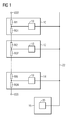
- FIG 1 illustrates a schematic circuit diagram of a modular electronic apparatus according to a preferred embodiment of the present invention.
- the modular electronic apparatus comprises a plurality of electronic elements. Further, the modular electronic apparatus may include also electric components.
- the modular electronic apparatus includes a plurality of the circuit units 10, 12 and 14.
- a first circuit unit 10, a second circuit unit 12 and an n-th circuit unit 14 are represented.
- the circuit units 10, 12 and 14 are exchangeable.
- each circuit unit 10, 12 and 14 includes a printed circuit board attachable in a slot.
- the modular electronic apparatus includes an internal communication bus 22.
- Each circuit unit 10, 12 and 14 is connected to the internal communication bus 22.
- the internal communication bus 22 is connected to and controlled by a master unit 16.
- Each circuit unit 10, 12 and 14 includes a control unit 18.
- the master unit 16 includes a master control unit 20.
- the control units 18 and the master control unit 20 include a digital interface in each case.
- the control units 18 and the master control unit 20 are connected to the internal communication bus 22 via the digital interface.
- Each circuit unit 10, 12 and 14 comprises two serial resistor elements.
- the circuit units 10, 12 and 14 may include more than two serial resistor elements.
- the first circuit unit 10 comprises a first input resistor element RI1 and a first output resistor element RO1.
- the second circuit unit 12 comprises a second input resistor element RI2 and a second output resistor element R02.
- the n-th circuit unit 14 comprises an n-th input resistor element RIN and an n-th output resistor element RON.
- the serial resistor elements form a voltage divided on each circuit unit 10, 12 and 14.
- serial resistor elements RI1, RO1, RI2, R02, RIN and RON of each circuit unit 10, 12 and 14 are connected in series.
- the series of the serial resistor elements RI1, RO1, RI2, R02, RIN and RON forms an ID wire.
- the first input resistor element RI1 of the first circuit unit 10 is connected to a first voltage terminal VDD.
- the n-th output resistor element of the n-th circuit unit 14 is connected to a second voltage terminal VSS.
- a characteristic voltage is applied on the connection point between the input resistor element and output resistor element of each circuit unit 10, 12 and 14 a characteristic voltage is applied.
- the circuit units 10, 12 and 14 have different characteristic voltages.
- Each control unit 18 includes an AD converter.
- the characteristic voltage is an analogue value and applied to an input of the AD converter.
- the analogue value of the characteristic voltage is converted to a digital value and applied to the internal communication bus 22.
- the characteristic voltage of the circuit unit 10, 12 or 14 depends on the position of said circuit unit 10, 12 or 14 within the ID wire and on the values of the resistor elements RI1, RO1, RI2, R02, RIN and RON. By this concept it is impossible, that different circuit units 10, 12 and 14 have the same characteristic voltages.
- the first input resistor element RI1 of the first circuit unit 10 is connected or connectable by a jumper to the first voltage terminal VDD.
- the n-th output resistor element RON of the n-th circuit unit 14 is connected or connectable by another jumper to the second voltage terminal VSS.
- a supply voltage VCC of the AD converter is divided through a number N(ID) of unit IDs.
- the number N(ID) of the unit IDs corresponds with the number of circuit units 10, 12 and 14.
- the circuit units 10, 12 and 14 are informed by the master unit 16 about the total number of circuit units 10, 12 and 14 connected to the internal communication bus 22. Different threshold levels are defined for each different number of circuit units 10, 12 and 14 on the internal communication bus 22. When the circuit units 10, 12 and 14 receive the total number, then each circuit unit 10, 12 and 14 selects a table with threshold levels fitting with the number of IDs. Said table is a part of a matrix stored in a memory of each circuit unit 10, 12 and 14. The matrix includes a plurality of such tables, wherein each table corresponds with the total number of circuit units 10, 12 and 14 in the modular electronic apparatus.
- the table may be calculated by formulas (3).
- the verification of the correct configuration is made by a response of the control units 10, 12 and 14.
- Said response includes the AD value AD(ID) and the configured ID.
- AD(ID) In order to avoid any collisions on the internal communication bus 22 the control units 10, 12 and 14 response with a delay corresponding to the AD values AD(ID).
- the master unit 16 is able to understand, if all expected control units 10, 12 and 14 have been configured correctly.
- the master unit 16 examine the responses received from the control units 10, 12 and 14. It is necessary that the responses from all expected control units 10, 12 and 14 have been received, wherein the control units 10, 12 and 14 must have configured themselves different ID.
- the AD values AD(ID) are still available and helpful to reveal the origins of eventual mistakes in the configuration.
- the master unit 16 queries for the number of circuit units 10, 12 and 14. In an initial message the master unit 16 asks the circuit units 10, 12 and 14 to respond with their AD values AD(ID) only. During this step the IDs are not yet configured. Then, the master unit 16 can examine the received responses. After the integrity of the information has been examined, the number of circuit units 10, 12 and 14 are configured by sending a new message. The number of IDs is set. The integrity of the responses may be determined by examining the AD values AD(ID) of all received messages. The AD values AD(ID) must be exist in an even range from VCC to VSS without any gaps.
- the matrix below includes a plurality of tables, wherein each table corresponds with one total number of circuit units 10, 12 and 14.
- the possible numbers of circuit units 10, 12 and 14 extend from two up to twelve.
- the matrix relates to the case, in which all the resistor elements RI1, RO1, RI2, R02, ..., RIN and RON have the same resistance values.
- the fractions in the matrix are the AD values AD(ID).
- Each column of AD values AD(ID) corresponds with one total number of the circuit units 10, 12 and 14.
- the AD values AD(ID) are identical or correspond with the characteristic voltages of the circuit units 10, 12 and 14. Further, the AD values correspond with the position of the circuit units 10, 12 and 14 in the series of the resistor elements RI1, RO1, RI2, R02, RIN and RON.
- the knowledge of the total number of circuit units 10, 12 and 14 selects the corresponding table within the matrix.
- the AD value AD(ID) measured for each circuit unit 10, 12 and 14 assigns the ID to the corresponding circuit unit 10, 12 and 14, respectively.
- the master control unit 20 informs the circuit units 10, 12 and 14 via the internal communication bus 22 about the total number of circuit units 10, 12 and 14. Then, each circuit unit 10, 12 and 14 detects its AD value AD(ID) by the control unit 18. Knowing the total number of the interconnected circuit units 10, 12 and 14, each circuit unit 10, 12 and 14 can obtain its ID from the corresponding table within the matrix.
- the content of the matrix above is stored in a memory of each circuit unit 10, 12 and 14.
- the memory is a part of the control unit 18 of each circuit unit 10, 12 and 14.
- the modular electronic apparatus includes three circuit units 10, 12 and 14, then the circuit units 10, 12 and 14 are informed by the master control unit 20. Then, each circuit unit 10, 12 and 14 detects its AD value AD(ID) and picks up said value in the column for the three circuit units.
- the third circuit unit 14 detects the value "1/6" and finds its ID "1".
- the second circuit unit 12 detects the value "3/6" and finds its ID "2”.
- the first circuit unit 10 detects the value "5/6" and finds its ID "2".
- the system of the present invention may be realized in hardware or a combination of hardware and software.
- the present invention can also be embedded in a computer program product which comprises all the features enabling the implementation of the methods described herein. Further, when loaded in computer system, said computer program product is able to carry out these methods.
- the modular electronic apparatus may be a domestic appliance.
- the modular electronic apparatus is a cooking oven and/or a cooking hob.
- the modular electronic apparatus may by an arbitrary modular electronic and/or electric device.
Landscapes
- Engineering & Computer Science (AREA)
- Computer Networks & Wireless Communication (AREA)
- Signal Processing (AREA)
- Theoretical Computer Science (AREA)
- Physics & Mathematics (AREA)
- General Physics & Mathematics (AREA)
- Dc Digital Transmission (AREA)
- Programmable Controllers (AREA)
- Information Transfer Systems (AREA)
Abstract
Description
- The present invention relates to a modular electronic and/or electric apparatus including a plurality of circuit units connected by an internal communication bus. In particular, the present invention relates to a modular domestic appliance including a plurality of circuit units connected by an internal communication bus.
- In a modular electronic and/or electric apparatus with a plurality of circuit units and an internal bus communication system, a unique ID has to be assigned for each of said circuit units. There are different methods for assigning the IDs for the circuit units. Some methods require manual labour or extensive hardware.
- It is an object of the present invention to provide a modular electronic apparatus with a plurality of circuit units and an internal communication bus, which allows an automatic and dynamic setting of IDs for the circuit units.
- The object of the present invention is achieved by the modular electronic and/or electric apparatus according to claim 1.
- The modular electronic and/or electric apparatus according to the present invention includes a plurality of circuit units connected by an internal communication bus, wherein:
- the circuit unit comprises at least two serial resistor elements forming a voltage divider,
- the resistor elements of the circuit units are serially connected and form an ID wire,
- the ID wire is interconnected between a first voltage terminal and a second voltage terminal,
- the circuit unit comprises at least one analogue-digital converter,
- a connection point between two resistor elements of one circuit unit is connected to an analogue input terminal of the analogue-digital converter,
- a digital output terminal of the analogue-digital converter is connected to the internal communication bus, and
- the modular electronic and/or electric apparatus comprises a master unit connected to the internal communication bus.
- The main idea of the present invention is the voltage divider on each circuit unit, wherein the voltage dividers of all circuit units are serially connected and form the ID wire. Each circuit unit has an own characterizing voltage value on its connection point of its voltage divider. Each circuit unit has a different characterizing voltage. The ID of the circuit unit depends on said characterizing voltage. The circuit units are arbitrarily exchangeable. The characterizing voltage depends on the position of the circuit unit and on the resistance values of its resistor elements.
- According to a preferred embodiment of the present invention the circuit unit comprises two serial resistor elements and one connection point between said resistor elements. The two serial resistor elements of the circuit unit reduced the complexity of the modular electronic apparatus.
- Further, the circuit unit comprises at least one control unit. The control unit is easily connectable to the internal communication bus.
- In a similar way, the master unit comprises at least one master control unit. The master control unit is connectable to the circuit units and their control units via the internal communication bus by low complexity.
- For example, the resistor elements of the ID wire have the same resistance values. In this case, the characterizing voltages of the circuit units are equally spaced from each other.
- Further, a voltage between the connection point of the circuit unit and the first voltage terminal or second voltage terminal of the ID wire defines an analogue value of an ID of said circuit unit.
- In a similar way, a value at the digital output terminal of the analogue-digital converter of the circuit unit corresponding with the analogue value of the ID of said circuit unit defines a digital value of the ID.
- In particular, a matrix of values is provided, wherein a column or line of said matrix corresponds with a total number of circuit units and the line or column, respectively, of the matrix corresponds with the ID of one of the circuit units.
- For example, the matrix is stored in the control unit of each circuit unit, so that each circuit unit is able to find its ID.
- Alternatively, the matrix is calculable in the control unit by at least one formula, so that each circuit unit is able to find its ID.
- For example, the modular electronic and/or electric apparatus is a domestic appliance.
- In particular, the modular electronic and/or electric apparatus is a cooking oven and/or a cooking hob.
- Further, the present invention relates to a method for determining the IDs for the circuit units of the modular electronic and/or electric apparatus mentioned above, wherein said method comprises the steps of:
- informing each circuit unit about the total number of circuit units connected to the internal communication bus by the master unit,
- detecting a voltage at the connection point between two resistor elements of each circuit unit, and
- determining the ID for each circuit unit on the basis of the total number of circuit units and the voltage at the connection point between the resistor elements of said circuit unit according to a predetermined assignment rule.
- In particular, the assignment rule is stored in each circuit unit and/or is calculable in the control unit by at least one formula.
- Novel and inventive features of the present invention are set forth in the appended claims.
- The present invention will be described in further detail with reference to the drawings, in which
- FIG 1
- illustrates a schematic circuit diagram of a modular electronic apparatus according to a preferred embodiment of the present invention.
-
FIG 1 illustrates a schematic circuit diagram of a modular electronic apparatus according to a preferred embodiment of the present invention. The modular electronic apparatus comprises a plurality of electronic elements. Further, the modular electronic apparatus may include also electric components. - The modular electronic apparatus includes a plurality of the
circuit units FIG 1 afirst circuit unit 10, asecond circuit unit 12 and an n-th circuit unit 14 are represented. Preferably, thecircuit units circuit unit - The modular electronic apparatus includes an
internal communication bus 22. Eachcircuit unit internal communication bus 22. Theinternal communication bus 22 is connected to and controlled by amaster unit 16. Eachcircuit unit control unit 18. In a similar way, themaster unit 16 includes amaster control unit 20. Thecontrol units 18 and themaster control unit 20 include a digital interface in each case. Thecontrol units 18 and themaster control unit 20 are connected to theinternal communication bus 22 via the digital interface. - Each
circuit unit circuit units first circuit unit 10 comprises a first input resistor element RI1 and a first output resistor element RO1. Accordingly, thesecond circuit unit 12 comprises a second input resistor element RI2 and a second output resistor element R02. In a similar way, the n-th circuit unit 14 comprises an n-th input resistor element RIN and an n-th output resistor element RON. The serial resistor elements form a voltage divided on eachcircuit unit - Further, the serial resistor elements RI1, RO1, RI2, R02, RIN and RON of each
circuit unit first circuit unit 10 is connected to a first voltage terminal VDD. In a similar way, the n-th output resistor element of the n-th circuit unit 14 is connected to a second voltage terminal VSS. On the connection point between the input resistor element and output resistor element of eachcircuit unit circuit units - The connection point between the input resistor element and output resistor element of each
circuit unit control unit 18 of thecorresponding circuit unit control unit 18 includes an AD converter. The characteristic voltage is an analogue value and applied to an input of the AD converter. In the AD converter the analogue value of the characteristic voltage is converted to a digital value and applied to theinternal communication bus 22. The characteristic voltage of thecircuit unit circuit unit different circuit units - For example, the first input resistor element RI1 of the
first circuit unit 10 is connected or connectable by a jumper to the first voltage terminal VDD. In a similar way, the n-th output resistor element RON of the n-th circuit unit 14 is connected or connectable by another jumper to the second voltage terminal VSS. - The conversion of the analogue value of the characteristic voltage into the digital unit ID is described below.
- A supply voltage VCC of the AD converter is divided through a number N(ID) of unit IDs. The number N(ID) of the unit IDs corresponds with the number of
circuit units 
defines the number N(step) of the steps of the AD conversion between two adjacent digital ID values. - An AD value AD(ID) for a given digital ID value D(ID) is defined by

wherein the range of the AD value AD(ID) starts with AD(ID) = 1. A threshold value TH(ID) between two adjacent IDs is given by
- The
circuit units master unit 16 about the total number ofcircuit units internal communication bus 22. Different threshold levels are defined for each different number ofcircuit units internal communication bus 22. When thecircuit units circuit unit circuit unit circuit units - Alternatively, the table may be calculated by formulas (3).
- The verification of the correct configuration is made by a response of the
control units internal communication bus 22 thecontrol units master unit 16 is able to understand, if all expectedcontrol units master unit 16 examine the responses received from thecontrol units control units control units - Another possible implementation is a completely dynamic configuration of the IDs. The
master unit 16 queries for the number ofcircuit units master unit 16 asks thecircuit units master unit 16 can examine the received responses. After the integrity of the information has been examined, the number ofcircuit units - The matrix below includes a plurality of tables, wherein each table corresponds with one total number of
circuit units circuit units Number of circuit units: ID: two circuit units three circuit units four circuit units ··· twelve circuit units 1 1/2 1/6 1/2 1/12 2 3/4 3/6 3/4 3/12 3 5/6 1/2 5/12 4 3/4 7/12 ··· 9/12 12 11/12 - The fractions in the matrix are the AD values AD(ID). Each column of AD values AD(ID) corresponds with one total number of the
circuit units circuit units circuit units circuit units circuit unit corresponding circuit unit - The
master control unit 20 informs thecircuit units internal communication bus 22 about the total number ofcircuit units circuit unit control unit 18. Knowing the total number of theinterconnected circuit units circuit unit - The content of the matrix above is stored in a memory of each
circuit unit control unit 18 of eachcircuit unit - For example, if the modular electronic apparatus includes three
circuit units circuit units master control unit 20. Then, eachcircuit unit third circuit unit 14 detects the value "1/6" and finds its ID "1". Thesecond circuit unit 12 detects the value "3/6" and finds its ID "2". Thefirst circuit unit 10 detects the value "5/6" and finds its ID "2". - The system of the present invention may be realized in hardware or a combination of hardware and software.
- The present invention can also be embedded in a computer program product which comprises all the features enabling the implementation of the methods described herein. Further, when loaded in computer system, said computer program product is able to carry out these methods.
- The modular electronic apparatus may be a domestic appliance. For example, the modular electronic apparatus is a cooking oven and/or a cooking hob. In general, the modular electronic apparatus may by an arbitrary modular electronic and/or electric device.
- While the invention has been described in detail herein in accordance with certain preferred embodiments thereof, many modifications and changes therein may be effected by those skilled in the art. Accordingly, it is intended by the appended claims to cover all such modifications and changes as fall within the true spirit and scope of the invention.
-
- 10
- first circuit unit
- 12
- second circuit unit
- 14
- n-th circuit unit
- 16
- master unit
- 18
- control unit
- 20
- master control unit
- 22
- internal communication bus
- RI1
- first input resistor element
- RO1
- first output resistor element
- RI2
- second input resistor element
- R02
- second output resistor element
- RIN
- n-th input resistor element
- RON
- n-th output resistor element
- VDD
- first voltage terminal
- VSS
- second voltage terminal
- VCC
- supply voltage
- N(ID)
- number of unit IDs
- N(Step)
- number of steps for AD conversion
- AD(ID)
- AD value
- TH(ID)
- threshold value
Claims (15)
- A modular electronic and/or electric apparatus including a plurality of circuit units (10, 12, 14) connected by an internal communication bus (22), wherein:- the circuit unit (10, 12, 14) comprises at least two serial resistor elements (RI1, RO1, RI2, R02, RIN, RON) forming a voltage divider,- the resistor elements (RI1, RO1, RI2, R02, RIN, RON) of the circuit units (10, 12, 14) are serially connected and form an ID wire,- the ID wire is interconnected between a first voltage terminal (VDD) and a second voltage terminal (VSS),- the circuit unit (10, 12, 14) comprises at least one analogue-digital converter,- a connection point between two resistor elements (RI1, RO1, RI2, R02, RIN, RON) of one circuit unit (10, 12, 14) is connected to an analogue input terminal of the analogue-digital converter,- a digital output terminal of the analogue-digital converter is connected to the internal communication bus (22), and- the modular electronic and/or electric apparatus comprises a master unit (16) connected to the internal communication bus (22).
- The apparatus according to claim 1,
characterized in that
the circuit unit (10, 12, 14) comprises two serial resistor elements (RI1, RO1, RI2, R02, RIN, RON) and one connection point between said resistor elements. - The apparatus according to claim 1 or 2,
characterized in that
the circuit unit (10, 12, 14) comprises at least one control unit (18). - The apparatus according to any one of the preceding claims,
characterized in that
the master unit (16) comprises at least one master control unit (20). - The apparatus according to any one of the preceding claims,
characterized in that
the resistor elements (RI1, RO1, RI2, R02, RIN, RON) of the ID wire have the same resistance values. - The apparatus according to any one of the preceding claims,
characterized in that
a voltage between the connection point of the circuit unit (10, 12, 14) and the first voltage terminal (VDD) or second voltage terminal (VSS) of the ID wire defines an analogue value of an ID of said circuit unit (10, 12, 14). - The apparatus according to claim 6,
characterized in that
a value at the digital output terminal of the analogue-digital converter of the circuit unit (10, 12, 14) corresponding with the analogue value of the ID of said circuit unit (10, 12, 14) defines a digital value of the ID. - The apparatus according to any one of the preceding claims,
characterized in that
a matrix of values is provided, wherein a column or line of said matrix corresponds with a total number of circuit units (10, 12, 14) and a line or column, respectively, of the matrix corresponds with the ID of one of the circuit units (10, 12, 14). - The apparatus according to claim 8,
characterized in that
the values of the matrix correspond with the analogue value of the ID. - The apparatus according to any one of the claims 3 to 9,
characterized in that
the matrix is stored in the control unit (18) of each circuit unit (10, 12, 14), so that each circuit unit (10, 12, 14) is able to find its ID. - The apparatus according to any one of the claims 3 to 9,
characterized in that
the matrix is calculable in the control unit (18) by at least one formula, so that each circuit unit (10, 12, 14) is able to find its ID. - The apparatus according to any one of the preceding claims,
characterized in that
the modular electronic and/or electric apparatus is a domestic appliance. - The apparatus according to claim 11,
characterized in that
the modular electronic and/or electric apparatus is a cooking oven and/or a cooking hob. - A method for determining IDs for the circuit units (10, 12, 14) of the modular electronic and/or electric apparatus according to any one of the preceding claims, wherein said method comprises the steps of:- informing each circuit unit (10, 12, 14) about the total number of circuit units (10, 12, 14) connected to the internal communication bus (22) by the master unit (16),- detecting a voltage at the connection point between two resistor elements (RI1, RO1, RI2, R02, RIN, RON) of the circuit unit (10, 12, 14), and- determining the ID for each circuit unit (10, 12, 14) on the basis of the total number of circuit units (10, 12, 14) connected to the internal communication bus (22) and the voltage at the connection point between the resistor elements (RI1, RO1, RI2, R02, RIN, RON) of said circuit unit (10, 12, 14) according to a predetermined assignment rule.
- The method according to claim 14,
characterized in that
the assignment rule is stored in each circuit unit (10, 12, 14) and/or is calculable in the control unit (18) by at least one formula.
Priority Applications (5)
| Application Number | Priority Date | Filing Date | Title |
|---|---|---|---|
| EP12193125.7A EP2733856B1 (en) | 2012-11-19 | 2012-11-19 | A modular electronic apparatus including a plurality of circuit units connected by an internal communication bus |
| CN201380051059.7A CN104685795B (en) | 2012-11-19 | 2013-11-11 | Modular unit comprising multiple circuit units connected by an internal communication bus |
| AU2013346969A AU2013346969B2 (en) | 2012-11-19 | 2013-11-11 | A modular electronic apparatus including a plurality of circuit units connected by an internal communication bus |
| PCT/EP2013/073479 WO2014076027A1 (en) | 2012-11-19 | 2013-11-11 | A modular electronic apparatus including a plurality of circuit units connected by an internal communication bus |
| US14/432,670 US10009037B2 (en) | 2012-11-19 | 2013-11-11 | Modular electronic apparatus including a plurality of circuit units connected by an internal communication bus |
Applications Claiming Priority (1)
| Application Number | Priority Date | Filing Date | Title |
|---|---|---|---|
| EP12193125.7A EP2733856B1 (en) | 2012-11-19 | 2012-11-19 | A modular electronic apparatus including a plurality of circuit units connected by an internal communication bus |
Publications (2)
| Publication Number | Publication Date |
|---|---|
| EP2733856A1 true EP2733856A1 (en) | 2014-05-21 |
| EP2733856B1 EP2733856B1 (en) | 2020-01-15 |
Family
ID=47562972
Family Applications (1)
| Application Number | Title | Priority Date | Filing Date |
|---|---|---|---|
| EP12193125.7A Active EP2733856B1 (en) | 2012-11-19 | 2012-11-19 | A modular electronic apparatus including a plurality of circuit units connected by an internal communication bus |
Country Status (5)
| Country | Link |
|---|---|
| US (1) | US10009037B2 (en) |
| EP (1) | EP2733856B1 (en) |
| CN (1) | CN104685795B (en) |
| AU (1) | AU2013346969B2 (en) |
| WO (1) | WO2014076027A1 (en) |
Families Citing this family (2)
| Publication number | Priority date | Publication date | Assignee | Title |
|---|---|---|---|---|
| CN110362522B (en) * | 2019-05-31 | 2023-05-12 | 中兴通讯股份有限公司 | Method, device and system for obtaining module identification |
| CN116406034B (en) * | 2023-03-15 | 2026-03-03 | 上海宇航系统工程研究所 | Spacecraft heater control and state detection system |
Citations (2)
| Publication number | Priority date | Publication date | Assignee | Title |
|---|---|---|---|---|
| US20030048474A1 (en) * | 2001-08-29 | 2003-03-13 | Samsung Electronics Co., Ltd. | Apparatus for and method of recognizing trays in a printer |
| EP1326172A2 (en) * | 2001-12-28 | 2003-07-09 | Texas Instruments Incorporated | Communication Method and Apparatus for Assigning Device Identifier |
Family Cites Families (9)
| Publication number | Priority date | Publication date | Assignee | Title |
|---|---|---|---|---|
| US5235159A (en) * | 1988-03-25 | 1993-08-10 | General Electric Company | Control system, method of operating a heating apparatus and controlled heating apparatus |
| US5293447A (en) * | 1992-06-02 | 1994-03-08 | The United States Of America As Represented By The Secretary Of Commerce | Photovoltaic solar water heating system |
| US6974934B2 (en) * | 2002-12-30 | 2005-12-13 | Intel Corporation | Remote reference resistor |
| US9221056B2 (en) * | 2007-08-29 | 2015-12-29 | Canon U.S. Life Sciences, Inc. | Microfluidic devices with integrated resistive heater electrodes including systems and methods for controlling and measuring the temperatures of such heater electrodes |
| CN101482749A (en) * | 2008-01-11 | 2009-07-15 | 鸿富锦精密工业(深圳)有限公司 | Automatic addressing system of master device to slave device |
| CN101841590B (en) * | 2009-03-16 | 2013-01-09 | 联芯科技有限公司 | Terminal equipment software and hardware self-adaptive matching method and terminal equipment using same |
| CN101699423A (en) * | 2009-09-28 | 2010-04-28 | 上海华为技术有限公司 | Hardware identifying method, device and system |
| CN201628954U (en) | 2009-11-18 | 2010-11-10 | 华为终端有限公司 | Electronic product identification device and electronic equipment |
| US9353486B2 (en) * | 2011-08-16 | 2016-05-31 | Railway Equipment Company, Inc. | Load balanced track switch heating |
-
2012
- 2012-11-19 EP EP12193125.7A patent/EP2733856B1/en active Active
-
2013
- 2013-11-11 WO PCT/EP2013/073479 patent/WO2014076027A1/en not_active Ceased
- 2013-11-11 CN CN201380051059.7A patent/CN104685795B/en not_active Expired - Fee Related
- 2013-11-11 AU AU2013346969A patent/AU2013346969B2/en not_active Ceased
- 2013-11-11 US US14/432,670 patent/US10009037B2/en active Active
Patent Citations (2)
| Publication number | Priority date | Publication date | Assignee | Title |
|---|---|---|---|---|
| US20030048474A1 (en) * | 2001-08-29 | 2003-03-13 | Samsung Electronics Co., Ltd. | Apparatus for and method of recognizing trays in a printer |
| EP1326172A2 (en) * | 2001-12-28 | 2003-07-09 | Texas Instruments Incorporated | Communication Method and Apparatus for Assigning Device Identifier |
Also Published As
| Publication number | Publication date |
|---|---|
| AU2013346969B2 (en) | 2017-04-20 |
| EP2733856B1 (en) | 2020-01-15 |
| US20150249460A1 (en) | 2015-09-03 |
| CN104685795A (en) | 2015-06-03 |
| US10009037B2 (en) | 2018-06-26 |
| CN104685795B (en) | 2019-03-22 |
| WO2014076027A1 (en) | 2014-05-22 |
| AU2013346969A1 (en) | 2015-04-02 |
Similar Documents
| Publication | Publication Date | Title |
|---|---|---|
| EP2330742A1 (en) | Electronic device and apparatus for identifying electronic product | |
| US11231968B2 (en) | Method for identifying bus nodes in a bus system | |
| US9835667B2 (en) | Method for detecting a wiring fault in a capacitive sensor | |
| EP2779788A1 (en) | A method for assigning induction coils of an induction cooking hob and an induction cooking hob | |
| EP2733856B1 (en) | A modular electronic apparatus including a plurality of circuit units connected by an internal communication bus | |
| EP4054036B1 (en) | Circuit breaker identification method and apparatus, and device | |
| CN111610427A (en) | Finished product testing method, circuit board testing method and device | |
| US11782862B2 (en) | Method of assigning addresses to bus participants | |
| EP4564183A1 (en) | I2c bus system and method for selectively connecting in an i2c bus system a plurality of slaves to a master | |
| EP4312409A1 (en) | Protocol for autoconfiguration of communication network | |
| CN105653242A (en) | Timing method and apparatus | |
| US20080104294A1 (en) | Method for operation of a bus system | |
| CN110988734B (en) | Fault detection device, method and equipment | |
| CN107210744B (en) | Connector component information detection | |
| EP2757383A1 (en) | Rectifier identification method and device | |
| EP4312408A1 (en) | Method of autoconfiguration of communication network | |
| US11615036B2 (en) | Method for identifying address of slave devices, system, and device applying the method | |
| CN106790753A (en) | The multiple automatic recognition systems and coding method from control plate of lamp interior | |
| CN110418121B (en) | Electronic component and projection equipment | |
| KR102239008B1 (en) | Sensor module for a vehicle and method for assigning sensor id using the system | |
| US20100207656A1 (en) | Detection circuit and a method for detecting a wrong supply voltage | |
| JPH0457145B2 (en) | ||
| EP2184828A1 (en) | A detection circuit and a method for detecting a wrong power line connection | |
| CN100389412C (en) | Method for Automatically Distinguishing Positions of Multiple Serial Devices | |
| CN114268516A (en) | Slave station address detection device and slave station equipment |
Legal Events
| Date | Code | Title | Description |
|---|---|---|---|
| PUAI | Public reference made under article 153(3) epc to a published international application that has entered the european phase |
Free format text: ORIGINAL CODE: 0009012 |
|
| 17P | Request for examination filed |
Effective date: 20121119 |
|
| AK | Designated contracting states |
Kind code of ref document: A1 Designated state(s): AL AT BE BG CH CY CZ DE DK EE ES FI FR GB GR HR HU IE IS IT LI LT LU LV MC MK MT NL NO PL PT RO RS SE SI SK SM TR |
|
| AX | Request for extension of the european patent |
Extension state: BA ME |
|
| R17P | Request for examination filed (corrected) |
Effective date: 20141022 |
|
| RBV | Designated contracting states (corrected) |
Designated state(s): AL AT BE BG CH CY CZ DE DK EE ES FI FR GB GR HR HU IE IS IT LI LT LU LV MC MK MT NL NO PL PT RO RS SE SI SK SM TR |
|
| STAA | Information on the status of an ep patent application or granted ep patent |
Free format text: STATUS: EXAMINATION IS IN PROGRESS |
|
| 17Q | First examination report despatched |
Effective date: 20180704 |
|
| GRAP | Despatch of communication of intention to grant a patent |
Free format text: ORIGINAL CODE: EPIDOSNIGR1 |
|
| STAA | Information on the status of an ep patent application or granted ep patent |
Free format text: STATUS: GRANT OF PATENT IS INTENDED |
|
| INTG | Intention to grant announced |
Effective date: 20190816 |
|
| GRAS | Grant fee paid |
Free format text: ORIGINAL CODE: EPIDOSNIGR3 |
|
| GRAA | (expected) grant |
Free format text: ORIGINAL CODE: 0009210 |
|
| STAA | Information on the status of an ep patent application or granted ep patent |
Free format text: STATUS: THE PATENT HAS BEEN GRANTED |
|
| AK | Designated contracting states |
Kind code of ref document: B1 Designated state(s): AL AT BE BG CH CY CZ DE DK EE ES FI FR GB GR HR HU IE IS IT LI LT LU LV MC MK MT NL NO PL PT RO RS SE SI SK SM TR |
|
| REG | Reference to a national code |
Ref country code: CH Ref legal event code: EP Ref country code: GB Ref legal event code: FG4D |
|
| REG | Reference to a national code |
Ref country code: IE Ref legal event code: FG4D |
|
| REG | Reference to a national code |
Ref country code: DE Ref legal event code: R096 Ref document number: 602012067246 Country of ref document: DE |
|
| REG | Reference to a national code |
Ref country code: AT Ref legal event code: REF Ref document number: 1226073 Country of ref document: AT Kind code of ref document: T Effective date: 20200215 |
|
| REG | Reference to a national code |
Ref country code: NL Ref legal event code: MP Effective date: 20200115 |
|
| REG | Reference to a national code |
Ref country code: LT Ref legal event code: MG4D |
|
| PG25 | Lapsed in a contracting state [announced via postgrant information from national office to epo] |
Ref country code: NO Free format text: LAPSE BECAUSE OF FAILURE TO SUBMIT A TRANSLATION OF THE DESCRIPTION OR TO PAY THE FEE WITHIN THE PRESCRIBED TIME-LIMIT Effective date: 20200415 Ref country code: PT Free format text: LAPSE BECAUSE OF FAILURE TO SUBMIT A TRANSLATION OF THE DESCRIPTION OR TO PAY THE FEE WITHIN THE PRESCRIBED TIME-LIMIT Effective date: 20200607 Ref country code: FI Free format text: LAPSE BECAUSE OF FAILURE TO SUBMIT A TRANSLATION OF THE DESCRIPTION OR TO PAY THE FEE WITHIN THE PRESCRIBED TIME-LIMIT Effective date: 20200115 Ref country code: NL Free format text: LAPSE BECAUSE OF FAILURE TO SUBMIT A TRANSLATION OF THE DESCRIPTION OR TO PAY THE FEE WITHIN THE PRESCRIBED TIME-LIMIT Effective date: 20200115 Ref country code: RS Free format text: LAPSE BECAUSE OF FAILURE TO SUBMIT A TRANSLATION OF THE DESCRIPTION OR TO PAY THE FEE WITHIN THE PRESCRIBED TIME-LIMIT Effective date: 20200115 |
|
| PG25 | Lapsed in a contracting state [announced via postgrant information from national office to epo] |
Ref country code: BG Free format text: LAPSE BECAUSE OF FAILURE TO SUBMIT A TRANSLATION OF THE DESCRIPTION OR TO PAY THE FEE WITHIN THE PRESCRIBED TIME-LIMIT Effective date: 20200415 Ref country code: IS Free format text: LAPSE BECAUSE OF FAILURE TO SUBMIT A TRANSLATION OF THE DESCRIPTION OR TO PAY THE FEE WITHIN THE PRESCRIBED TIME-LIMIT Effective date: 20200515 Ref country code: SE Free format text: LAPSE BECAUSE OF FAILURE TO SUBMIT A TRANSLATION OF THE DESCRIPTION OR TO PAY THE FEE WITHIN THE PRESCRIBED TIME-LIMIT Effective date: 20200115 Ref country code: LV Free format text: LAPSE BECAUSE OF FAILURE TO SUBMIT A TRANSLATION OF THE DESCRIPTION OR TO PAY THE FEE WITHIN THE PRESCRIBED TIME-LIMIT Effective date: 20200115 Ref country code: GR Free format text: LAPSE BECAUSE OF FAILURE TO SUBMIT A TRANSLATION OF THE DESCRIPTION OR TO PAY THE FEE WITHIN THE PRESCRIBED TIME-LIMIT Effective date: 20200416 Ref country code: HR Free format text: LAPSE BECAUSE OF FAILURE TO SUBMIT A TRANSLATION OF THE DESCRIPTION OR TO PAY THE FEE WITHIN THE PRESCRIBED TIME-LIMIT Effective date: 20200115 |
|
| REG | Reference to a national code |
Ref country code: DE Ref legal event code: R097 Ref document number: 602012067246 Country of ref document: DE |
|
| PG25 | Lapsed in a contracting state [announced via postgrant information from national office to epo] |
Ref country code: SK Free format text: LAPSE BECAUSE OF FAILURE TO SUBMIT A TRANSLATION OF THE DESCRIPTION OR TO PAY THE FEE WITHIN THE PRESCRIBED TIME-LIMIT Effective date: 20200115 Ref country code: DK Free format text: LAPSE BECAUSE OF FAILURE TO SUBMIT A TRANSLATION OF THE DESCRIPTION OR TO PAY THE FEE WITHIN THE PRESCRIBED TIME-LIMIT Effective date: 20200115 Ref country code: SM Free format text: LAPSE BECAUSE OF FAILURE TO SUBMIT A TRANSLATION OF THE DESCRIPTION OR TO PAY THE FEE WITHIN THE PRESCRIBED TIME-LIMIT Effective date: 20200115 Ref country code: EE Free format text: LAPSE BECAUSE OF FAILURE TO SUBMIT A TRANSLATION OF THE DESCRIPTION OR TO PAY THE FEE WITHIN THE PRESCRIBED TIME-LIMIT Effective date: 20200115 Ref country code: ES Free format text: LAPSE BECAUSE OF FAILURE TO SUBMIT A TRANSLATION OF THE DESCRIPTION OR TO PAY THE FEE WITHIN THE PRESCRIBED TIME-LIMIT Effective date: 20200115 Ref country code: RO Free format text: LAPSE BECAUSE OF FAILURE TO SUBMIT A TRANSLATION OF THE DESCRIPTION OR TO PAY THE FEE WITHIN THE PRESCRIBED TIME-LIMIT Effective date: 20200115 Ref country code: LT Free format text: LAPSE BECAUSE OF FAILURE TO SUBMIT A TRANSLATION OF THE DESCRIPTION OR TO PAY THE FEE WITHIN THE PRESCRIBED TIME-LIMIT Effective date: 20200115 Ref country code: CZ Free format text: LAPSE BECAUSE OF FAILURE TO SUBMIT A TRANSLATION OF THE DESCRIPTION OR TO PAY THE FEE WITHIN THE PRESCRIBED TIME-LIMIT Effective date: 20200115 |
|
| REG | Reference to a national code |
Ref country code: AT Ref legal event code: MK05 Ref document number: 1226073 Country of ref document: AT Kind code of ref document: T Effective date: 20200115 |
|
| PLBE | No opposition filed within time limit |
Free format text: ORIGINAL CODE: 0009261 |
|
| STAA | Information on the status of an ep patent application or granted ep patent |
Free format text: STATUS: NO OPPOSITION FILED WITHIN TIME LIMIT |
|
| 26N | No opposition filed |
Effective date: 20201016 |
|
| PG25 | Lapsed in a contracting state [announced via postgrant information from national office to epo] |
Ref country code: AT Free format text: LAPSE BECAUSE OF FAILURE TO SUBMIT A TRANSLATION OF THE DESCRIPTION OR TO PAY THE FEE WITHIN THE PRESCRIBED TIME-LIMIT Effective date: 20200115 |
|
| PGFP | Annual fee paid to national office [announced via postgrant information from national office to epo] |
Ref country code: FR Payment date: 20201120 Year of fee payment: 9 Ref country code: IT Payment date: 20201124 Year of fee payment: 9 Ref country code: DE Payment date: 20201119 Year of fee payment: 9 |
|
| PG25 | Lapsed in a contracting state [announced via postgrant information from national office to epo] |
Ref country code: PL Free format text: LAPSE BECAUSE OF FAILURE TO SUBMIT A TRANSLATION OF THE DESCRIPTION OR TO PAY THE FEE WITHIN THE PRESCRIBED TIME-LIMIT Effective date: 20200115 Ref country code: SI Free format text: LAPSE BECAUSE OF FAILURE TO SUBMIT A TRANSLATION OF THE DESCRIPTION OR TO PAY THE FEE WITHIN THE PRESCRIBED TIME-LIMIT Effective date: 20200115 |
|
| PG25 | Lapsed in a contracting state [announced via postgrant information from national office to epo] |
Ref country code: MC Free format text: LAPSE BECAUSE OF FAILURE TO SUBMIT A TRANSLATION OF THE DESCRIPTION OR TO PAY THE FEE WITHIN THE PRESCRIBED TIME-LIMIT Effective date: 20200115 |
|
| REG | Reference to a national code |
Ref country code: CH Ref legal event code: PL |
|
| GBPC | Gb: european patent ceased through non-payment of renewal fee |
Effective date: 20201119 |
|
| PG25 | Lapsed in a contracting state [announced via postgrant information from national office to epo] |
Ref country code: LU Free format text: LAPSE BECAUSE OF NON-PAYMENT OF DUE FEES Effective date: 20201119 |
|
| REG | Reference to a national code |
Ref country code: BE Ref legal event code: MM Effective date: 20201130 |
|
| PG25 | Lapsed in a contracting state [announced via postgrant information from national office to epo] |
Ref country code: CH Free format text: LAPSE BECAUSE OF NON-PAYMENT OF DUE FEES Effective date: 20201130 Ref country code: LI Free format text: LAPSE BECAUSE OF NON-PAYMENT OF DUE FEES Effective date: 20201130 |
|
| PG25 | Lapsed in a contracting state [announced via postgrant information from national office to epo] |
Ref country code: IE Free format text: LAPSE BECAUSE OF NON-PAYMENT OF DUE FEES Effective date: 20201119 |
|
| PG25 | Lapsed in a contracting state [announced via postgrant information from national office to epo] |
Ref country code: GB Free format text: LAPSE BECAUSE OF NON-PAYMENT OF DUE FEES Effective date: 20201119 |
|
| PG25 | Lapsed in a contracting state [announced via postgrant information from national office to epo] |
Ref country code: TR Free format text: LAPSE BECAUSE OF FAILURE TO SUBMIT A TRANSLATION OF THE DESCRIPTION OR TO PAY THE FEE WITHIN THE PRESCRIBED TIME-LIMIT Effective date: 20200115 Ref country code: MT Free format text: LAPSE BECAUSE OF FAILURE TO SUBMIT A TRANSLATION OF THE DESCRIPTION OR TO PAY THE FEE WITHIN THE PRESCRIBED TIME-LIMIT Effective date: 20200115 Ref country code: CY Free format text: LAPSE BECAUSE OF FAILURE TO SUBMIT A TRANSLATION OF THE DESCRIPTION OR TO PAY THE FEE WITHIN THE PRESCRIBED TIME-LIMIT Effective date: 20200115 |
|
| REG | Reference to a national code |
Ref country code: DE Ref legal event code: R119 Ref document number: 602012067246 Country of ref document: DE |
|
| PG25 | Lapsed in a contracting state [announced via postgrant information from national office to epo] |
Ref country code: MK Free format text: LAPSE BECAUSE OF FAILURE TO SUBMIT A TRANSLATION OF THE DESCRIPTION OR TO PAY THE FEE WITHIN THE PRESCRIBED TIME-LIMIT Effective date: 20200115 Ref country code: AL Free format text: LAPSE BECAUSE OF FAILURE TO SUBMIT A TRANSLATION OF THE DESCRIPTION OR TO PAY THE FEE WITHIN THE PRESCRIBED TIME-LIMIT Effective date: 20200115 |
|
| PG25 | Lapsed in a contracting state [announced via postgrant information from national office to epo] |
Ref country code: BE Free format text: LAPSE BECAUSE OF NON-PAYMENT OF DUE FEES Effective date: 20201130 |
|
| PG25 | Lapsed in a contracting state [announced via postgrant information from national office to epo] |
Ref country code: DE Free format text: LAPSE BECAUSE OF NON-PAYMENT OF DUE FEES Effective date: 20220601 |
|
| PG25 | Lapsed in a contracting state [announced via postgrant information from national office to epo] |
Ref country code: FR Free format text: LAPSE BECAUSE OF NON-PAYMENT OF DUE FEES Effective date: 20211130 |
|
| PG25 | Lapsed in a contracting state [announced via postgrant information from national office to epo] |
Ref country code: IT Free format text: LAPSE BECAUSE OF NON-PAYMENT OF DUE FEES Effective date: 20211119 |