EP2733784B1 - Antenne plane en F inverse - Google Patents
Antenne plane en F inverse Download PDFInfo
- Publication number
- EP2733784B1 EP2733784B1 EP13185731.0A EP13185731A EP2733784B1 EP 2733784 B1 EP2733784 B1 EP 2733784B1 EP 13185731 A EP13185731 A EP 13185731A EP 2733784 B1 EP2733784 B1 EP 2733784B1
- Authority
- EP
- European Patent Office
- Prior art keywords
- substrate
- pifa
- electrode
- emitting electrode
- antenna
- Prior art date
- Legal status (The legal status is an assumption and is not a legal conclusion. Google has not performed a legal analysis and makes no representation as to the accuracy of the status listed.)
- Not-in-force
Links
Images


Classifications
-
- H—ELECTRICITY
- H01—ELECTRIC ELEMENTS
- H01Q—ANTENNAS, i.e. RADIO AERIALS
- H01Q1/00—Details of, or arrangements associated with, antennas
- H01Q1/27—Adaptation for use in or on movable bodies
- H01Q1/273—Adaptation for carrying or wearing by persons or animals
-
- H—ELECTRICITY
- H01—ELECTRIC ELEMENTS
- H01Q—ANTENNAS, i.e. RADIO AERIALS
- H01Q1/00—Details of, or arrangements associated with, antennas
- H01Q1/40—Radiating elements coated with or embedded in protective material
-
- H—ELECTRICITY
- H01—ELECTRIC ELEMENTS
- H01Q—ANTENNAS, i.e. RADIO AERIALS
- H01Q9/00—Electrically-short antennas having dimensions not more than twice the operating wavelength and consisting of conductive active radiating elements
- H01Q9/04—Resonant antennas
- H01Q9/0407—Substantially flat resonant element parallel to ground plane, e.g. patch antenna
- H01Q9/0421—Substantially flat resonant element parallel to ground plane, e.g. patch antenna with a shorting wall or a shorting pin at one end of the element
Definitions
- the present invention relates to, for example, a planar inverted-F antenna suitable for implanting into a living body.
- An antenna used for a communication device implanted in a living body such as the human body or animal body is preferably as compact and thin as possible. Loss of electric waves is large in a living body. Therefore, an antenna used for a communication device implanted in a living body is desired to be capable of communicating with other communication devices even in such a medium as a living body causing large electric wave loss.
- antennas each equipped with an emitting electrode folded at one or more portions thereof (Refer to, for instance, Published Japanese Translation of PCT International Publication for Patent Application (Kohyo) No. 2006-505973 , Published Japanese Translation of PCT International Publication for Patent Application (Kohyo) No. 2002-533001 , Japanese Laid-Open Patent Publication No. 2001-53535 and Japanese Laid-Open Patent Publication No. 2006-74351 ).
- These antennas are, however, have not been implanted in a living body for use thereof. Therefore, with the antennas as described above, it is impossible to reduce negative effects caused by electric wave loss in a living body, and the antennas are not suitable for use together with communication devices implanted in a living body.
- US 2010/0019985 discloses an antenna assembly for an implantable medical device.
- the implantable medical device comprises a hermetically sealed housing, typically formed of titanium materials, and electronics, including a transceiver, disposed therein.
- An antenna is disposed in an air, gas or plastic dielectric filled compartment within a header, which is attached to the housing.
- the header is premolded so as to create the compartment.
- the antenna is then placed within the compartment, which is then sealed.
- an antenna as compact as possible for the purpose of reducing a load to a living body.
- an object of the present invention is to provide a planar inverted-F antenna which is suitable for implanting into a living body and which can be made compact.
- a planar inverted-F antenna includes a first substrate made of a dielectric material; a grounding electrode disposed on a first surface of the first substrate; an emitting electrode disposed to be opposite to the grounding electrode so as to sandwich the first substrate, formed into an S-shape, and having a short-circuiting point short-circuited to the grounding electrode located on an end of the emitting electrode, and a feeding point at power is fed and which is located away from the short-circuiting point with a distance where the characteristic impedance of the planar inverted-F antenna to electric waves having a certain designed wavelength is a certain value; and a second substrate provided to cover the entire emitting electrode and made of a dielectric material, and an insulating layer disposed to cover the entire grounding electrode together with the first substrate and insulating a living body in which the planar inverted-F antenna is implanted from the grounding electrode, wherein the dielectric constant of the insulating material layer
- PIFA planar inverted-F antenna
- the entire surface of an emitting electrode is covered with a dielectric material. Furthermore, in the PIFA, for reducing negative effects to the living body, also the entire surface of the grounding electrode is covered with an insulator. In addition, since the emitting electrode is in the form of an S-shape, it is possible to make the emitting electrode compact, which in turn makes the PIFA compact.
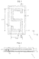
- FIG. 1 is a transparent plan view illustrating a surface of a substrate in a PIFA 1 according to one embodiment
- FIG. 2 is a cross-sectional side view illustrating the PIFA 1 cut along line AA' in FIG.1 and viewed in the direction represented by an arrow head.
- the horizontal direction in FIG. 1 is the x-axial direction and the vertical direction is the y-axial direction.
- the vertical direction to the surface of the PIFA 1 is the z-axial direction.
- a plane parallel to the surface of the PIFA 1 is the horizontal plane.
- the PIFA 1 includes a substrate 10, a grounding electrode 11 disposed on the bottom surface of the substrate 10, and an emitting electrode 12 which is disposed on the top surface of the substrate 10 and which is opposed to the grounding electrode 11 so as to sandwich the substrate 10. Furthermore, the PIFA 1 includes a superstrate 13 superimposed on the substrate 10 so as to sandwich the emitting electrode 12 and cover the entire surface of the emitting electrode 12, and an insulating material layer 14 disposed under the substrate 10 so as to sandwich the grounding electrode 11 and cover the entire grounding electrode 11.
- the PIFA 1 is implanted in a living body so that, for instance, the top surface of the substrate 10 is closer to a surface of the living body than the bottom surface of the substrate 10 and the top surface of the substrate 10 is substantially parallel to the surface of the living body.
- a communication circuit (not illustrated) for sending or receiving electric waves using the PIFA 1 is positioned, for instance, under the bottom surface of the insulating material layer 14. This communication circuit may be covered with an insulating material.
- the substrate 10 supports the grounding electrode 11 and the emitting electrode 12.
- the substrate 10 is made of, for instance, a dielectric material including glass and ceramics.
- the substrate 10 may be made of another dielectric material suitable for superimposing and excellent in biocompatibility such as acrylic resin.
- the thickness of the substrate 10 is decided so that the characteristic impedance of the PIFA 1 is a certain value such as 50 ⁇ or 75 ⁇ .
- the grounding electrode 11 is a planar conductor connected to ground, and in this embodiment, the grounding electrode 11 covers the entire bottom surface of the substrate 10.
- the emitting electrode 12 is a slender and planar conductor disposed between the top surface of the substrate 10 and the bottom surface of the superstrate 13.
- the emitting electrode 12 is in the form of an S-shape, and an edge 12a thereof functions as a short-circuiting point connected, for instance, through a via hole formed on the substrate 10 to the grounding electrode 11.
- a feed point 12b is provided at a position away from the short-circuiting point 12a by a distance at which the characteristic impedance of the PIFA 1 is a certain value (such as 50 ⁇ or 75 ⁇ ) for the design wavelength of the electric wave transmitted from or received by the PIFA 1.
- the emitting electrode 12 is connected at the feed point 12b, for instance, through a via hole formed on the substrate 10 to the grounding electrode 11 and is electrically fed.
- the length from the feed point 12b to the other edge point of the emitting electrode 12 is set to substantially one fourth of the design wavelength.
- both the x-axial and y-axial lengths are shorter than one fourth (1/4) of the design wavelength. Because of the form, three portions of the emitting electrode 12, which are different from each other, are included within a certain width along the x-axial direction, and therefore the size of the emitting electrode 12 on the horizontal surface 12 is small.
- both edges of the emitting electrode 12 are folded along the y-axial direction so that the short-circuiting point 12a and the other edge portion of the emitting electrode 12 are opposed to each other. Therefore, the size of the emitting electrode 12 in the x-axial direction becomes smaller. Because of the features described above, it is possible to downsize the PIFA 1. For instance, when the PIFA 1 transmits and receives electric wave with the frequency in a 400 MHz band, which is one of the frequency bands used in a body area network, as illustrated in FIG. 1 , the length of the emitting electrode 12 in the x-axial direction is 11 mm, while the length of the emitting electrode 12 in the y-axial direction is 26 mm.
- grounding electrode 11 and the emitting electrode 12 are made of, for instance, metal such as aluminum, copper, gold, silver, or nickel, an alloy of the metals, or other materials having conductivity.
- the superstrate 13 matches the impedance of the PIFA 1 to that of a living body in which the PIFA 1 is implanted.
- the superstrate 13 is made of a dielectric material including glass and ceramics.
- the superstrate 13 may be made of other dielectric material suited to superimposing and excellent in biocompatibility such as acrylic resin.
- the substrate 10 and the superstrate 13 may be made of the same dielectric material or of different dielectric materials respectively.
- the thickness of the superstrate 13 is decided so that the impedance of the PIFA 1 matches to that of a living body in which the PIFA 1 is implanted. Effects of the thickness of the superstrate 13 over matching between the impedance of the PIFA 1 and that of a living body will be described below.
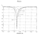
- FIG. 3 is a view illustrating results of simulations for an S parameter of the PIFA 1 when the thicknesses of the superstrate are 0.5 mm, 1 mm, and 1.5 mm, respectively.
- the dielectric constant of the substrate 10 and that of the superstrate 13 are 10.2 respectively, and the thickness of the substrate 10 is 1.5 mm.
- the thickness of the insulating material layer 14 is 0.5 mm, and the dielectric constant of the insulating material layer 14 is 2.5.
- the PIFA 1 has a dielectric constant of 46.7 and the PIFA 1 is implanted between a living body layer with a thickness of 5 mm and a living body layer with a thickness of 10 mm with a dielectric tangent of 0.69 S/m.
- the horizontal axis indicates a frequency [GHz], while the vertical axis indicates a value of S 11 parameter [dB].
- Graph 300 indicates the frequency characteristic of S 11 parameter of the PIFA 1 when the thickness of the superstrate 13 is 0.5 mm.
- Graph 310 indicates the frequency characteristic of S 11 parameter of the PIFA 1 when the thickness of the superstrate 13 is 1.0 mm.
- Graph 320 indicates the frequency characteristic of S 11 parameter of the PIFA 1 when the thickness of the superstrate 13 is 1.5 mm. It is to be noted that each of the frequency characteristics was calculated by the electric field analysis using the finite element method.
- the dielectric constant of a living body is very high, for instance, in the range from 40 to 50, while the dielectric constant of a dielectric body suited to implant in a living body is lower than that of a living body.
- the thickness of the superstrate 13 is 0.5 mm, but the thickness of the superstrate 13 may be set to a value, for instance, in the range from 0.5 mm to 1.5 mm, since the value of S 11 parameter is lower than -6dB which is a target value for an antenna available for radio communication.
- the insulating material layer 14 keeps the grounding electrode 11 insulated from a living body in which the PIFA 1 is implanted. Because of this insulation, negative effects caused by electric waves transmitted from or received by the PIFA 1 can be reduced. For the purpose of efficiently in reducing negative effects by a current flowing in the grounding electrode 11, the dielectric constant of the insulating material layer 14 is lower than the dielectric constant of the substrate 10 and that of the superstrate 13.
- the insulating material layer 14 is preferably excellent in biocompatibility, because the PIFA 1 is in contact with a living body. Therefore, the insulating material layer 14 is preferably made of, for instance, is a fluororesin.
- FIG.4A and FIG. 4B are views illustrating results of simulations, by means of the finite element method, for the distributions of current densities in the grounding electrode 11 when an insulating material layer 14 is removed from the PIFA 1 and when an insulating material layer 14 is present.
- the PIFA 1 receives an electric wave with a frequency of 424 MHz.
- the size of the emitting electrode 12 is as illustrated in FIG. 1 , and the sizes and physical characteristics of each substrate are the same as those of each substrate in the simulation illustrated in FIG. 3 . It is to be noted that the thickness of the superstrate 13 is 1.5 mm.
- FIG. 5 is a view illustrating results of simulations for an S parameter of the PIFA 1 when various forms of the insulating material layer 14 are employed.
- the size of the emitting electrode 12 is as illustrated in FIG. 1
- the size and physical characteristics of each substrate are the same as those of each substrate in the simulation illustrated in FIG. 3 .
- the thickness of the superstrate 13 is 1.5 mm.
- Graph 500 illustrates the frequency characteristics of S 11 parameter of the PIFA 1 when the insulating material layer 14 is provided under the substrate 10 so that the insulating material layer 14 covers only the grounding electrode 11.
- Graph 510 illustrates the frequency characteristics of S 11 parameter of the PIFA 1 when the insulating material layer 14 is formed so that the insulating material layer 14 covers the entire side surface of the PIFA 1, i.e., so that the PIFA 1 covers not only the grounding electrode 11, but also side faces of the emitting electrode 12 and the superstrate 13.
- Graph 520 illustrates the frequency characteristics of S 11 parameter of the PIFA 1 when the insulating material layer 14 is formed so that the insulating layer 14 covers the entire PIFA 1.
- Each of the frequency characteristics is calculated by means of the electric field analysis using the finite element method. As is obvious from graphs 500 to 520, it can be understood that, when the insulating material layer 14 is formed to cover the grounding electrode and other sections such as the emitting electrode 12, the S 11 parameter is larger as compared to when the insulating material layer 14 is formed to cover only the grounding electrode 11, and that the communicating performance of the PIFA 1 is lower.
- the insulating material layer 14 does not surround the emitting electrode 12 and the superstrate 13 and is provided only under the substrate 10.
- the insulating material layer 14 is provided to cover the bottom and side faces of the grounding electrode 11 without surrounding the side face of the substrate 10.
- the grounding electrode 11 and the emitting electrode 12 are fixed to the top or bottom surface of the substrate 10 by means of, for instance, etching or adhesion.
- the substrate 10 and the superstrate 13 also are fixed to each other, for instance, by adhesion.
- the grounding electrode 11 and the insulating material layer 14 are fixed to each other, for instance, by adhesion.
- FIG. 6 is a view illustrating a result of simulation for a radiation pattern of electric wave having a frequency of 405 MHz formed around the PIFA 1.
- the size of the emitting electrode 12 is as illustrated in FIG. 1
- the sizes and physical characteristics of the substrates are the same as those of the substrates used in the simulations illustrated in FIG. 3 .
- the thickness of the superstrate 13 is 1.5 mm.
- the gain is in the range from about -32 dB to -30 dB.
- the PIFA includes a dielectric layer covering an emitting electrode. Therefore, even when the PIFA is implanted in a living body where electric wave loss is high, reflection of electric wave between the living body and the PIFA is suppressed, which enables communication with a communication device outside the living body. Since this PIFA includes an insulating material layer covering a grounding electrode, it is possible to reduce negative effects by a current flowing through the grounding electrode to the living body. Furthermore, since an emitting electrode in the PIFA is folded into an S-shape, it is possible to make the PIFA compact in the horizontal direction.
- FIG. 7A and FIG. 7B are transparent plan views illustrating forms of emitting electrodes of PIFAs according to modifications, respectively.
- the length of an emitting electrode 12' in the y-axial direction is shorter than that of the emitting electrode 12 illustrated in FIG. 1 , while the length thereof in the x-axial direction is longer than that of the emitting electrode 12.
- the length in the x-axial direction is 15 mm, and that in the y-axial direction is 18 mm.
- an edge portion 12c of the emitting electrode 12' in the opposite side from the short-circuiting point 12a is positioned in the inner side from the right edge portion of the emitting electrode 12'. Because of this configuration, the emitting electrode 12' is parallel to the x-axial direction near the edge portion 12c.
- an emitting electrode 12" is further folded in comparison to the emitting electrode 12 illustrated in FIG. 1 so that the portion near an edge of the emitting electrode 12" where the short-circuiting point 12b is positioned and the portion near the other edge of the emitting electrode 12" are parallel to the x-axial direction. Because of this configuration, the section of the emitting electrode 12" between the short-circuiting point 12a and the feed point 12b has a U-shaped form. As a result, five portions of the emitting electrode 12" are parallel to the x-axis, so that the size of the PIFA in the horizontal direction can be reduced.
- the emitting electrode may be folded at any angle other than a right angle.
- the emitting electrode may be a curved line.
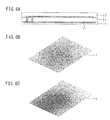
- FIG. 8A is a sectional side view of a PIFA in still another modification.
- the grounding electrode 11 is smaller than the bottom surface of the substrate 10, and the bottom surface of the substrate 10 around the grounding electrode 11 directly and closely contacts the insulating material layer 14. Because of the structure described above, in the PIFA in this modification, the sizes of the substrate 10, the superstrate 13, and the insulating material layer 14 are identical.
- FIG. 8B is a view illustrating a result of simulation for distribution of current densities in the grounding electrode in the variant illustrated in FIG. 8A.
- FIG. 8C is a view illustrating, as a comparative example, a result of simulation for distribution of current densities in a grounding electrode when the grounding electrode covers the entire bottom surface of the substrate.
- the PIFA 1 receives electric waves with a frequency of 405 MHz.
- the size of the emitting electrode is as illustrated in FIG.7A , and the size and physical characteristics of each substrate are the same as employed in the simulation illustrated in FIG. 3 .
- the thickness of the superstrate 13 is 1.5 mm.
Claims (3)
- Antenne plane en F inversé (1) implantable dans un corps vivant, qui comprend :un premier substrat (10) composé d'un matériau diélectrique ;une électrode de mise à la masse (11) disposée sur une première surface du premier substrat ;une électrode d'émission (12, 12', 12") disposée afin d'être opposée à l'électrode de mise à la masse (11) de façon à prendre en sandwich le premier substrat (10), l'électrode d'émission (12, 12', 12") ayant la forme d'un S, et ayant un point de court-circuit (12a) mis en court-circuit avec l'électrode de mise à la masse (11) au niveau d'une partie de bord de celle-ci, un point d'alimentation (12b) au niveau duquel une énergie est fournie, et qui se trouve à l'écart du point de court-circuit (12a) selon une distance à laquelle l'impédance caractéristique de l'antenne plane en F inversé (1) pour les ondes électriques qui présentent une certaine longueur d'onde possède une certaine valeur ;un second substrat (13) disposé afin de recouvrir l'électrode d'émission (12, 12', 12") entière avec le premier substrat (10), et composé d'un matériau diélectrique ; etune couche de matériau isolant (14) disposée afin de recouvrir l'électrode de mise à la masse (11) entière avec le premier substrat (10), et qui isole de l'électrode de mise à la masse (11) un corps vivant dans lequel l'antenne plane en F inversé (1) est implantée, la constante diélectrique de la couche de matériau isolant (14) étant inférieure aux constantes diélectriques du premier substrat (10) et du second substrat (13).
- Antenne plane en F inversé selon la revendication 1, dans laquelle l'électrode d'émission (12, 12', 12") est soudée de sorte que la partie de bord de l'électrode d'émission (12, 12', 12") au niveau de laquelle se trouve le point de court-circuit (12a) et l'autre partie de bord de l'électrode d'émission (12, 12', 12") soient opposées.
- Antenne plane en F inversé selon la revendication 1, dans laquelle une section de la partie de bord de l'électrode d'émission (12, 12', 12") dans laquelle le point de court-circuit (12a) se trouve par rapport au point d'alimentation de l'électrode d'émission (12, 12', 12") possède une forme de U.
Applications Claiming Priority (1)
| Application Number | Priority Date | Filing Date | Title |
|---|---|---|---|
| JP2012253565A JP6003567B2 (ja) | 2012-11-19 | 2012-11-19 | 板状逆fアンテナ |
Publications (2)
| Publication Number | Publication Date |
|---|---|
| EP2733784A1 EP2733784A1 (fr) | 2014-05-21 |
| EP2733784B1 true EP2733784B1 (fr) | 2016-11-23 |
Family
ID=49223685
Family Applications (1)
| Application Number | Title | Priority Date | Filing Date |
|---|---|---|---|
| EP13185731.0A Not-in-force EP2733784B1 (fr) | 2012-11-19 | 2013-09-24 | Antenne plane en F inverse |
Country Status (4)
| Country | Link |
|---|---|
| US (1) | US9531063B2 (fr) |
| EP (1) | EP2733784B1 (fr) |
| JP (1) | JP6003567B2 (fr) |
| CN (1) | CN103825087B (fr) |
Families Citing this family (4)
| Publication number | Priority date | Publication date | Assignee | Title |
|---|---|---|---|---|
| CN104319468B (zh) * | 2014-10-15 | 2017-03-15 | 成都信息工程学院 | 弧形微带天线 |
| CN105024155B (zh) * | 2015-07-24 | 2018-04-27 | 华南理工大学 | 一种应用于生物医学遥测的加载互补开口环的圆极化天线 |
| CN107732420B (zh) * | 2017-10-27 | 2024-03-08 | 景昱医疗科技(苏州)股份有限公司 | 一种天线、植入式医疗器械及植入式医疗系统 |
| US11030507B2 (en) | 2017-11-29 | 2021-06-08 | Phoenix Solution Co., Ltd. | Antenna for RF tag, and RF tag |
Family Cites Families (17)
| Publication number | Priority date | Publication date | Assignee | Title |
|---|---|---|---|---|
| WO1996027219A1 (fr) * | 1995-02-27 | 1996-09-06 | The Chinese University Of Hong Kong | Antenne en f-inverse a serpentement |
| US5861019A (en) | 1997-07-25 | 1999-01-19 | Medtronic Inc. | Implantable medical device microstrip telemetry antenna |
| EP1135827A1 (fr) * | 1998-10-16 | 2001-09-26 | Paratek Microwave, Inc. | Materiaux dielectriques stratifies accordables en tension pour applications au micro-ondes |
| US6343208B1 (en) | 1998-12-16 | 2002-01-29 | Telefonaktiebolaget Lm Ericsson (Publ) | Printed multi-band patch antenna |
| JP4144127B2 (ja) * | 1999-08-13 | 2008-09-03 | Tdk株式会社 | マイクロストリップアンテナ |
| DE10029733A1 (de) * | 2000-06-23 | 2002-01-03 | Alcatel Sa | Antennenanordnung für Mobilfunktelefone |
| US7903043B2 (en) | 2003-12-22 | 2011-03-08 | Cardiac Pacemakers, Inc. | Radio frequency antenna in a header of an implantable medical device |
| JP2006505973A (ja) | 2002-11-07 | 2006-02-16 | フラクタス・ソシエダッド・アノニマ | 微小アンテナを含む集積回路パッケージ |
| JP2005012554A (ja) * | 2003-06-19 | 2005-01-13 | Kyocera Corp | アンテナ基板およびアンテナ装置 |
| JP4264040B2 (ja) | 2004-09-01 | 2009-05-13 | アルプス電気株式会社 | アンテナ装置 |
| US7414583B2 (en) * | 2004-12-08 | 2008-08-19 | Electronics And Telecommunications Research Institute | PIFA, RFID tag using the same and antenna impedance adjusting method thereof |
| US7504998B2 (en) * | 2004-12-08 | 2009-03-17 | Electronics And Telecommunications Research Institute | PIFA and RFID tag using the same |
| CN1901278A (zh) | 2005-07-22 | 2007-01-24 | 富士康(昆山)电脑接插件有限公司 | 平面倒f型天线及其制作方法 |
| US20100019985A1 (en) * | 2008-07-24 | 2010-01-28 | Jacob Bashyam | Header with integral antenna for implantable medical devices |
| US20100109966A1 (en) | 2008-10-31 | 2010-05-06 | Mateychuk Duane N | Multi-Layer Miniature Antenna For Implantable Medical Devices and Method for Forming the Same |
| US8285387B2 (en) * | 2008-12-12 | 2012-10-09 | Microchips, Inc. | Wireless communication with a medical implant |
| US8050771B2 (en) | 2008-12-29 | 2011-11-01 | Medtronic, Inc. | Phased array cofire antenna structure and method for operating the same |
-
2012
- 2012-11-19 JP JP2012253565A patent/JP6003567B2/ja not_active Expired - Fee Related
-
2013
- 2013-09-11 US US14/023,587 patent/US9531063B2/en not_active Expired - Fee Related
- 2013-09-24 EP EP13185731.0A patent/EP2733784B1/fr not_active Not-in-force
- 2013-09-30 CN CN201310461591.8A patent/CN103825087B/zh not_active Expired - Fee Related
Also Published As
| Publication number | Publication date |
|---|---|
| JP6003567B2 (ja) | 2016-10-05 |
| JP2014103515A (ja) | 2014-06-05 |
| CN103825087A (zh) | 2014-05-28 |
| US20140139383A1 (en) | 2014-05-22 |
| US9531063B2 (en) | 2016-12-27 |
| CN103825087B (zh) | 2017-04-12 |
| EP2733784A1 (fr) | 2014-05-21 |
Similar Documents
| Publication | Publication Date | Title |
|---|---|---|
| US8860613B2 (en) | Patch antenna | |
| US9368860B2 (en) | Patch antenna | |
| US9013355B1 (en) | L-shaped feed for a matching network for a microstrip antenna | |
| EP0697139B1 (fr) | Appareil emetteur et/ou recepteur portatif | |
| US7467014B2 (en) | Compact and conformal telemetry antennas for implantable medical devices | |
| EP1362614B1 (fr) | Antenne à plaque implantable | |
| CN101641826B (zh) | 天线布置和天线壳体 | |
| EP2733784B1 (fr) | Antenne plane en F inverse | |
| US6891505B2 (en) | EMC- arrangement for a device employing wireless data transfer | |
| JP2007521756A (ja) | スロット付き円筒アンテナ | |
| Ghosh et al. | Miniaturization of slot antennas using wire loading | |
| CN106785409A (zh) | 一种宽频带宽波束微带贴片天线 | |
| JP5104131B2 (ja) | 無線装置および無線装置が備えるアンテナ | |
| Seo et al. | Integration of resonant coil for wireless power transfer and implantable antenna for signal transfer | |
| US10014584B1 (en) | Slotted antenna with uniaxial dielectric covering | |
| Mitchell et al. | Search for high-performance probe-fed stacked patches using optimization | |
| EP3488494B1 (fr) | Antenne à cavité | |
| US6314275B1 (en) | Hand-held transmitting and/or receiving apparatus | |
| Shaheen et al. | Design of PIFA antenna for medical applications | |
| KR102250964B1 (ko) | 금속 매체가 탑재된 안테나 시스템 | |
| Tseng et al. | Design of broadband implantable antenna for biomedical application | |
| Malisuwan et al. | A broadband rectangular microstrip patch antenna for wireless communications | |
| Mishra et al. | Slotted Patch Antenna with Wide Bandwidth for In-body Biotelemetry Applications | |
| CN112864628A (zh) | 天线结构及可穿戴设备 | |
| CN117525832A (zh) | 一种天线、感知模块、传感器和电子设备 |
Legal Events
| Date | Code | Title | Description |
|---|---|---|---|
| PUAI | Public reference made under article 153(3) epc to a published international application that has entered the european phase |
Free format text: ORIGINAL CODE: 0009012 |
|
| 17P | Request for examination filed |
Effective date: 20130924 |
|
| AK | Designated contracting states |
Kind code of ref document: A1 Designated state(s): AL AT BE BG CH CY CZ DE DK EE ES FI FR GB GR HR HU IE IS IT LI LT LU LV MC MK MT NL NO PL PT RO RS SE SI SK SM TR |
|
| AX | Request for extension of the european patent |
Extension state: BA ME |
|
| R17P | Request for examination filed (corrected) |
Effective date: 20140826 |
|
| RBV | Designated contracting states (corrected) |
Designated state(s): AL AT BE BG CH CY CZ DE DK EE ES FI FR GB GR HR HU IE IS IT LI LT LU LV MC MK MT NL NO PL PT RO RS SE SI SK SM TR |
|
| GRAP | Despatch of communication of intention to grant a patent |
Free format text: ORIGINAL CODE: EPIDOSNIGR1 |
|
| INTG | Intention to grant announced |
Effective date: 20160617 |
|
| GRAS | Grant fee paid |
Free format text: ORIGINAL CODE: EPIDOSNIGR3 |
|
| GRAA | (expected) grant |
Free format text: ORIGINAL CODE: 0009210 |
|
| AK | Designated contracting states |
Kind code of ref document: B1 Designated state(s): AL AT BE BG CH CY CZ DE DK EE ES FI FR GB GR HR HU IE IS IT LI LT LU LV MC MK MT NL NO PL PT RO RS SE SI SK SM TR |
|
| REG | Reference to a national code |
Ref country code: GB Ref legal event code: FG4D |
|
| REG | Reference to a national code |
Ref country code: CH Ref legal event code: EP |
|
| REG | Reference to a national code |
Ref country code: IE Ref legal event code: FG4D |
|
| REG | Reference to a national code |
Ref country code: AT Ref legal event code: REF Ref document number: 848649 Country of ref document: AT Kind code of ref document: T Effective date: 20161215 |
|
| REG | Reference to a national code |
Ref country code: DE Ref legal event code: R096 Ref document number: 602013014331 Country of ref document: DE |
|
| PG25 | Lapsed in a contracting state [announced via postgrant information from national office to epo] |
Ref country code: LV Free format text: LAPSE BECAUSE OF FAILURE TO SUBMIT A TRANSLATION OF THE DESCRIPTION OR TO PAY THE FEE WITHIN THE PRESCRIBED TIME-LIMIT Effective date: 20161123 |
|
| REG | Reference to a national code |
Ref country code: LT Ref legal event code: MG4D |
|
| REG | Reference to a national code |
Ref country code: NL Ref legal event code: MP Effective date: 20161123 |
|
| REG | Reference to a national code |
Ref country code: AT Ref legal event code: MK05 Ref document number: 848649 Country of ref document: AT Kind code of ref document: T Effective date: 20161123 |
|
| PG25 | Lapsed in a contracting state [announced via postgrant information from national office to epo] |
Ref country code: GR Free format text: LAPSE BECAUSE OF FAILURE TO SUBMIT A TRANSLATION OF THE DESCRIPTION OR TO PAY THE FEE WITHIN THE PRESCRIBED TIME-LIMIT Effective date: 20170224 Ref country code: SE Free format text: LAPSE BECAUSE OF FAILURE TO SUBMIT A TRANSLATION OF THE DESCRIPTION OR TO PAY THE FEE WITHIN THE PRESCRIBED TIME-LIMIT Effective date: 20161123 Ref country code: LT Free format text: LAPSE BECAUSE OF FAILURE TO SUBMIT A TRANSLATION OF THE DESCRIPTION OR TO PAY THE FEE WITHIN THE PRESCRIBED TIME-LIMIT Effective date: 20161123 Ref country code: NO Free format text: LAPSE BECAUSE OF FAILURE TO SUBMIT A TRANSLATION OF THE DESCRIPTION OR TO PAY THE FEE WITHIN THE PRESCRIBED TIME-LIMIT Effective date: 20170223 Ref country code: NL Free format text: LAPSE BECAUSE OF FAILURE TO SUBMIT A TRANSLATION OF THE DESCRIPTION OR TO PAY THE FEE WITHIN THE PRESCRIBED TIME-LIMIT Effective date: 20161123 |
|
| PG25 | Lapsed in a contracting state [announced via postgrant information from national office to epo] |
Ref country code: RS Free format text: LAPSE BECAUSE OF FAILURE TO SUBMIT A TRANSLATION OF THE DESCRIPTION OR TO PAY THE FEE WITHIN THE PRESCRIBED TIME-LIMIT Effective date: 20161123 Ref country code: FI Free format text: LAPSE BECAUSE OF FAILURE TO SUBMIT A TRANSLATION OF THE DESCRIPTION OR TO PAY THE FEE WITHIN THE PRESCRIBED TIME-LIMIT Effective date: 20161123 Ref country code: PL Free format text: LAPSE BECAUSE OF FAILURE TO SUBMIT A TRANSLATION OF THE DESCRIPTION OR TO PAY THE FEE WITHIN THE PRESCRIBED TIME-LIMIT Effective date: 20161123 Ref country code: PT Free format text: LAPSE BECAUSE OF FAILURE TO SUBMIT A TRANSLATION OF THE DESCRIPTION OR TO PAY THE FEE WITHIN THE PRESCRIBED TIME-LIMIT Effective date: 20170323 Ref country code: ES Free format text: LAPSE BECAUSE OF FAILURE TO SUBMIT A TRANSLATION OF THE DESCRIPTION OR TO PAY THE FEE WITHIN THE PRESCRIBED TIME-LIMIT Effective date: 20161123 Ref country code: HR Free format text: LAPSE BECAUSE OF FAILURE TO SUBMIT A TRANSLATION OF THE DESCRIPTION OR TO PAY THE FEE WITHIN THE PRESCRIBED TIME-LIMIT Effective date: 20161123 Ref country code: AT Free format text: LAPSE BECAUSE OF FAILURE TO SUBMIT A TRANSLATION OF THE DESCRIPTION OR TO PAY THE FEE WITHIN THE PRESCRIBED TIME-LIMIT Effective date: 20161123 |
|
| PG25 | Lapsed in a contracting state [announced via postgrant information from national office to epo] |
Ref country code: RO Free format text: LAPSE BECAUSE OF FAILURE TO SUBMIT A TRANSLATION OF THE DESCRIPTION OR TO PAY THE FEE WITHIN THE PRESCRIBED TIME-LIMIT Effective date: 20161123 Ref country code: SK Free format text: LAPSE BECAUSE OF FAILURE TO SUBMIT A TRANSLATION OF THE DESCRIPTION OR TO PAY THE FEE WITHIN THE PRESCRIBED TIME-LIMIT Effective date: 20161123 Ref country code: EE Free format text: LAPSE BECAUSE OF FAILURE TO SUBMIT A TRANSLATION OF THE DESCRIPTION OR TO PAY THE FEE WITHIN THE PRESCRIBED TIME-LIMIT Effective date: 20161123 Ref country code: DK Free format text: LAPSE BECAUSE OF FAILURE TO SUBMIT A TRANSLATION OF THE DESCRIPTION OR TO PAY THE FEE WITHIN THE PRESCRIBED TIME-LIMIT Effective date: 20161123 Ref country code: CZ Free format text: LAPSE BECAUSE OF FAILURE TO SUBMIT A TRANSLATION OF THE DESCRIPTION OR TO PAY THE FEE WITHIN THE PRESCRIBED TIME-LIMIT Effective date: 20161123 |
|
| REG | Reference to a national code |
Ref country code: FR Ref legal event code: PLFP Year of fee payment: 5 |
|
| REG | Reference to a national code |
Ref country code: DE Ref legal event code: R097 Ref document number: 602013014331 Country of ref document: DE |
|
| PG25 | Lapsed in a contracting state [announced via postgrant information from national office to epo] |
Ref country code: BG Free format text: LAPSE BECAUSE OF FAILURE TO SUBMIT A TRANSLATION OF THE DESCRIPTION OR TO PAY THE FEE WITHIN THE PRESCRIBED TIME-LIMIT Effective date: 20170223 Ref country code: BE Free format text: LAPSE BECAUSE OF FAILURE TO SUBMIT A TRANSLATION OF THE DESCRIPTION OR TO PAY THE FEE WITHIN THE PRESCRIBED TIME-LIMIT Effective date: 20161123 Ref country code: IT Free format text: LAPSE BECAUSE OF FAILURE TO SUBMIT A TRANSLATION OF THE DESCRIPTION OR TO PAY THE FEE WITHIN THE PRESCRIBED TIME-LIMIT Effective date: 20161123 Ref country code: SM Free format text: LAPSE BECAUSE OF FAILURE TO SUBMIT A TRANSLATION OF THE DESCRIPTION OR TO PAY THE FEE WITHIN THE PRESCRIBED TIME-LIMIT Effective date: 20161123 |
|
| PLBE | No opposition filed within time limit |
Free format text: ORIGINAL CODE: 0009261 |
|
| STAA | Information on the status of an ep patent application or granted ep patent |
Free format text: STATUS: NO OPPOSITION FILED WITHIN TIME LIMIT |
|
| PGFP | Annual fee paid to national office [announced via postgrant information from national office to epo] |
Ref country code: FR Payment date: 20170803 Year of fee payment: 5 Ref country code: GB Payment date: 20170704 Year of fee payment: 5 Ref country code: DE Payment date: 20170622 Year of fee payment: 5 |
|
| 26N | No opposition filed |
Effective date: 20170824 |
|
| PG25 | Lapsed in a contracting state [announced via postgrant information from national office to epo] |
Ref country code: SI Free format text: LAPSE BECAUSE OF FAILURE TO SUBMIT A TRANSLATION OF THE DESCRIPTION OR TO PAY THE FEE WITHIN THE PRESCRIBED TIME-LIMIT Effective date: 20161123 |
|
| REG | Reference to a national code |
Ref country code: CH Ref legal event code: PL |
|
| PG25 | Lapsed in a contracting state [announced via postgrant information from national office to epo] |
Ref country code: MC Free format text: LAPSE BECAUSE OF FAILURE TO SUBMIT A TRANSLATION OF THE DESCRIPTION OR TO PAY THE FEE WITHIN THE PRESCRIBED TIME-LIMIT Effective date: 20161123 |
|
| REG | Reference to a national code |
Ref country code: IE Ref legal event code: MM4A |
|
| PG25 | Lapsed in a contracting state [announced via postgrant information from national office to epo] |
Ref country code: LU Free format text: LAPSE BECAUSE OF NON-PAYMENT OF DUE FEES Effective date: 20170924 |
|
| PG25 | Lapsed in a contracting state [announced via postgrant information from national office to epo] |
Ref country code: IE Free format text: LAPSE BECAUSE OF NON-PAYMENT OF DUE FEES Effective date: 20170924 Ref country code: LI Free format text: LAPSE BECAUSE OF NON-PAYMENT OF DUE FEES Effective date: 20170930 Ref country code: CH Free format text: LAPSE BECAUSE OF NON-PAYMENT OF DUE FEES Effective date: 20170930 |
|
| PG25 | Lapsed in a contracting state [announced via postgrant information from national office to epo] |
Ref country code: MT Free format text: LAPSE BECAUSE OF NON-PAYMENT OF DUE FEES Effective date: 20170924 |
|
| REG | Reference to a national code |
Ref country code: DE Ref legal event code: R119 Ref document number: 602013014331 Country of ref document: DE |
|
| GBPC | Gb: european patent ceased through non-payment of renewal fee |
Effective date: 20180924 |
|
| PG25 | Lapsed in a contracting state [announced via postgrant information from national office to epo] |
Ref country code: HU Free format text: LAPSE BECAUSE OF FAILURE TO SUBMIT A TRANSLATION OF THE DESCRIPTION OR TO PAY THE FEE WITHIN THE PRESCRIBED TIME-LIMIT; INVALID AB INITIO Effective date: 20130924 |
|
| PG25 | Lapsed in a contracting state [announced via postgrant information from national office to epo] |
Ref country code: DE Free format text: LAPSE BECAUSE OF NON-PAYMENT OF DUE FEES Effective date: 20190402 |
|
| PG25 | Lapsed in a contracting state [announced via postgrant information from national office to epo] |
Ref country code: FR Free format text: LAPSE BECAUSE OF NON-PAYMENT OF DUE FEES Effective date: 20180930 |
|
| PG25 | Lapsed in a contracting state [announced via postgrant information from national office to epo] |
Ref country code: CY Free format text: LAPSE BECAUSE OF NON-PAYMENT OF DUE FEES Effective date: 20161123 Ref country code: GB Free format text: LAPSE BECAUSE OF NON-PAYMENT OF DUE FEES Effective date: 20180924 |
|
| PG25 | Lapsed in a contracting state [announced via postgrant information from national office to epo] |
Ref country code: MK Free format text: LAPSE BECAUSE OF FAILURE TO SUBMIT A TRANSLATION OF THE DESCRIPTION OR TO PAY THE FEE WITHIN THE PRESCRIBED TIME-LIMIT Effective date: 20161123 |
|
| PG25 | Lapsed in a contracting state [announced via postgrant information from national office to epo] |
Ref country code: TR Free format text: LAPSE BECAUSE OF FAILURE TO SUBMIT A TRANSLATION OF THE DESCRIPTION OR TO PAY THE FEE WITHIN THE PRESCRIBED TIME-LIMIT Effective date: 20161123 |
|
| PG25 | Lapsed in a contracting state [announced via postgrant information from national office to epo] |
Ref country code: AL Free format text: LAPSE BECAUSE OF FAILURE TO SUBMIT A TRANSLATION OF THE DESCRIPTION OR TO PAY THE FEE WITHIN THE PRESCRIBED TIME-LIMIT Effective date: 20161123 Ref country code: IS Free format text: LAPSE BECAUSE OF FAILURE TO SUBMIT A TRANSLATION OF THE DESCRIPTION OR TO PAY THE FEE WITHIN THE PRESCRIBED TIME-LIMIT Effective date: 20170323 |