EP2731147B1 - Module de cellules solaires - Google Patents
Module de cellules solaires Download PDFInfo
- Publication number
- EP2731147B1 EP2731147B1 EP12808154.4A EP12808154A EP2731147B1 EP 2731147 B1 EP2731147 B1 EP 2731147B1 EP 12808154 A EP12808154 A EP 12808154A EP 2731147 B1 EP2731147 B1 EP 2731147B1
- Authority
- EP
- European Patent Office
- Prior art keywords
- busbar portion
- electrode
- finger portions
- busbar
- wiring
- Prior art date
- Legal status (The legal status is an assumption and is not a legal conclusion. Google has not performed a legal analysis and makes no representation as to the accuracy of the status listed.)
- Withdrawn - After Issue
Links
- 238000006243 chemical reaction Methods 0.000 claims description 21
- 239000012790 adhesive layer Substances 0.000 claims description 12
- 229920005989 resin Polymers 0.000 claims description 10
- 239000011347 resin Substances 0.000 claims description 10
- 239000000853 adhesive Substances 0.000 claims description 5
- 230000001070 adhesive effect Effects 0.000 claims description 5
- 239000002245 particle Substances 0.000 claims description 2
- 239000000758 substrate Substances 0.000 description 20
- 239000004065 semiconductor Substances 0.000 description 11
- 239000010410 layer Substances 0.000 description 8
- 239000000969 carrier Substances 0.000 description 5
- 230000000694 effects Effects 0.000 description 4
- 230000006798 recombination Effects 0.000 description 4
- 238000005215 recombination Methods 0.000 description 4
- 229910052751 metal Inorganic materials 0.000 description 3
- 239000002184 metal Substances 0.000 description 3
- 239000004698 Polyethylene Substances 0.000 description 2
- 238000009792 diffusion process Methods 0.000 description 2
- 239000002019 doping agent Substances 0.000 description 2
- 239000011521 glass Substances 0.000 description 2
- 229920002037 poly(vinyl butyral) polymer Polymers 0.000 description 2
- 229920000573 polyethylene Polymers 0.000 description 2
- VGGSQFUCUMXWEO-UHFFFAOYSA-N Ethene Chemical compound C=C VGGSQFUCUMXWEO-UHFFFAOYSA-N 0.000 description 1
- 239000005977 Ethylene Substances 0.000 description 1
- 239000000956 alloy Substances 0.000 description 1
- 229910045601 alloy Inorganic materials 0.000 description 1
- 229910052782 aluminium Inorganic materials 0.000 description 1
- 238000004873 anchoring Methods 0.000 description 1
- 239000000919 ceramic Substances 0.000 description 1
- 229920001577 copolymer Polymers 0.000 description 1
- 229910052802 copper Inorganic materials 0.000 description 1
- 230000007613 environmental effect Effects 0.000 description 1
- 239000011888 foil Substances 0.000 description 1
- 239000011810 insulating material Substances 0.000 description 1
- 239000000463 material Substances 0.000 description 1
- 150000002739 metals Chemical class 0.000 description 1
- -1 polyethylene Polymers 0.000 description 1
- 239000004814 polyurethane Substances 0.000 description 1
- 229910052709 silver Inorganic materials 0.000 description 1
- 230000008646 thermal stress Effects 0.000 description 1
Images


Classifications
-
- H—ELECTRICITY
- H01—ELECTRIC ELEMENTS
- H01L—SEMICONDUCTOR DEVICES NOT COVERED BY CLASS H10
- H01L31/00—Semiconductor devices sensitive to infrared radiation, light, electromagnetic radiation of shorter wavelength or corpuscular radiation and specially adapted either for the conversion of the energy of such radiation into electrical energy or for the control of electrical energy by such radiation; Processes or apparatus specially adapted for the manufacture or treatment thereof or of parts thereof; Details thereof
- H01L31/02—Details
- H01L31/02002—Arrangements for conducting electric current to or from the device in operations
- H01L31/02005—Arrangements for conducting electric current to or from the device in operations for device characterised by at least one potential jump barrier or surface barrier
- H01L31/02008—Arrangements for conducting electric current to or from the device in operations for device characterised by at least one potential jump barrier or surface barrier for solar cells or solar cell modules
- H01L31/0201—Arrangements for conducting electric current to or from the device in operations for device characterised by at least one potential jump barrier or surface barrier for solar cells or solar cell modules comprising specially adapted module bus-bar structures
-
- H—ELECTRICITY
- H01—ELECTRIC ELEMENTS
- H01L—SEMICONDUCTOR DEVICES NOT COVERED BY CLASS H10
- H01L31/00—Semiconductor devices sensitive to infrared radiation, light, electromagnetic radiation of shorter wavelength or corpuscular radiation and specially adapted either for the conversion of the energy of such radiation into electrical energy or for the control of electrical energy by such radiation; Processes or apparatus specially adapted for the manufacture or treatment thereof or of parts thereof; Details thereof
- H01L31/04—Semiconductor devices sensitive to infrared radiation, light, electromagnetic radiation of shorter wavelength or corpuscular radiation and specially adapted either for the conversion of the energy of such radiation into electrical energy or for the control of electrical energy by such radiation; Processes or apparatus specially adapted for the manufacture or treatment thereof or of parts thereof; Details thereof adapted as photovoltaic [PV] conversion devices
- H01L31/042—PV modules or arrays of single PV cells
- H01L31/048—Encapsulation of modules
-
- H—ELECTRICITY
- H01—ELECTRIC ELEMENTS
- H01L—SEMICONDUCTOR DEVICES NOT COVERED BY CLASS H10
- H01L31/00—Semiconductor devices sensitive to infrared radiation, light, electromagnetic radiation of shorter wavelength or corpuscular radiation and specially adapted either for the conversion of the energy of such radiation into electrical energy or for the control of electrical energy by such radiation; Processes or apparatus specially adapted for the manufacture or treatment thereof or of parts thereof; Details thereof
- H01L31/04—Semiconductor devices sensitive to infrared radiation, light, electromagnetic radiation of shorter wavelength or corpuscular radiation and specially adapted either for the conversion of the energy of such radiation into electrical energy or for the control of electrical energy by such radiation; Processes or apparatus specially adapted for the manufacture or treatment thereof or of parts thereof; Details thereof adapted as photovoltaic [PV] conversion devices
- H01L31/042—PV modules or arrays of single PV cells
- H01L31/05—Electrical interconnection means between PV cells inside the PV module, e.g. series connection of PV cells
- H01L31/0504—Electrical interconnection means between PV cells inside the PV module, e.g. series connection of PV cells specially adapted for series or parallel connection of solar cells in a module
- H01L31/0508—Electrical interconnection means between PV cells inside the PV module, e.g. series connection of PV cells specially adapted for series or parallel connection of solar cells in a module the interconnection means having a particular shape
-
- H—ELECTRICITY
- H01—ELECTRIC ELEMENTS
- H01L—SEMICONDUCTOR DEVICES NOT COVERED BY CLASS H10
- H01L31/00—Semiconductor devices sensitive to infrared radiation, light, electromagnetic radiation of shorter wavelength or corpuscular radiation and specially adapted either for the conversion of the energy of such radiation into electrical energy or for the control of electrical energy by such radiation; Processes or apparatus specially adapted for the manufacture or treatment thereof or of parts thereof; Details thereof
- H01L31/04—Semiconductor devices sensitive to infrared radiation, light, electromagnetic radiation of shorter wavelength or corpuscular radiation and specially adapted either for the conversion of the energy of such radiation into electrical energy or for the control of electrical energy by such radiation; Processes or apparatus specially adapted for the manufacture or treatment thereof or of parts thereof; Details thereof adapted as photovoltaic [PV] conversion devices
- H01L31/042—PV modules or arrays of single PV cells
- H01L31/05—Electrical interconnection means between PV cells inside the PV module, e.g. series connection of PV cells
- H01L31/0504—Electrical interconnection means between PV cells inside the PV module, e.g. series connection of PV cells specially adapted for series or parallel connection of solar cells in a module
- H01L31/0516—Electrical interconnection means between PV cells inside the PV module, e.g. series connection of PV cells specially adapted for series or parallel connection of solar cells in a module specially adapted for interconnection of back-contact solar cells
-
- Y—GENERAL TAGGING OF NEW TECHNOLOGICAL DEVELOPMENTS; GENERAL TAGGING OF CROSS-SECTIONAL TECHNOLOGIES SPANNING OVER SEVERAL SECTIONS OF THE IPC; TECHNICAL SUBJECTS COVERED BY FORMER USPC CROSS-REFERENCE ART COLLECTIONS [XRACs] AND DIGESTS
- Y02—TECHNOLOGIES OR APPLICATIONS FOR MITIGATION OR ADAPTATION AGAINST CLIMATE CHANGE
- Y02E—REDUCTION OF GREENHOUSE GAS [GHG] EMISSIONS, RELATED TO ENERGY GENERATION, TRANSMISSION OR DISTRIBUTION
- Y02E10/00—Energy generation through renewable energy sources
- Y02E10/50—Photovoltaic [PV] energy
Definitions
- the present invention relates to a solar module and solar cell.
- Solar modules are equipped with a plurality of solar cells which are connected electrically by a wiring member as shown, for example, in Patent Document 1.
- Patent Document 1 Laid-Open Patent Publication No. 2009-266848
- Document EP 2 081 237 A2 relates to a solar cell module including first and second solar cell arranged in a first direction and electrically connected by a wiring member, wherein the first and second solar cells each include a light-receiving surface receiving light, a back surface provided on the opposite side of the light-receiving surface, and p-side and n-side electrodes formed on the back surface.
- the wiring member is connected to the n-side electrode of the first solar cell at a first connecting point and connected to the p-side electrode of the second solar cell at a second connecting point, wherein in a planar view the first and second connecting points are located on a line intersecting with the first direction.
- JP 2011 054721 A discloses a solar module including a plurality of solar cells, each cell having first and second finger electrodes and first and second busbars.
- a wiring sheet connects adjacent cells by adhering to busbars and finger electrodes.
- the solar module of the present invention includes a plurality of solar cells, a wiring member, and an adhesive layer.
- Each solar cell has a photoelectric conversion unit, and first and second electrodes. The first and second electrodes are provided on the photoelectric conversion unit. Between adjacent solar cells, the wiring member electrically connects the first electrode of one solar cell to the second electrode of the other solar cell.
- the adhesive layer bonds the wiring member and the solar cells.
- the wiring member has an insulating substrate and wiring provided on the insulating substrate.
- the first and second electrodes each have a plurality of finger portions.
- the wiring has an adherend portion which is bonded to the solar cells by the adhesive layer. The adherend portion is provided over the finger portions and the section of the photoelectric conversion unit in which a finger portions are not provided.
- the solar cell of the present invention includes a photoelectric conversion unit, and a first and a second electrode.
- the first and second electrodes are provided on the photoelectric conversion unit.
- the first and second electrodes are connected to the wiring member via the adhesive layer.
- Each of the first and second electrodes has a plurality of finger portions, a linear first busbar portion, and a second busbar portion.
- the first busbar portion is connected electrically to at least one of the plurality of finger portions.
- the second busbar portion is connected electrically to any of the plurality of finger portions not connected to the first busbar portion.
- the second busbar portion is arranged to the outside of the first busbar portion in the direction of extension of the first busbar portion.
- the electrical resistance of the first busbar portion is higher than the electrical resistance of the second busbar portion.
- the present invention is able to provide a solar module in which peeling of the wiring member from the solar cells has been suppressed.
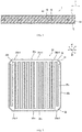
- FIG. 1 is a simplified cross-sectional view of the solar module 1 in an embodiment.
- the solar module 1 includes a solar cell string 10.
- the solar cell string 10 is arranged between a first protecting member 11 positioned on the side of the light-receiving surface, and a second protecting member 12 positioned on the side of the back surface.
- a bonding layer 13 is provided between the first protecting member 11 and the second protecting member 12.
- the solar cell string 10 is sealed by the bonding layer 13.
- the first protecting member 11 can be a glass substrate or a resin substrate.
- the second protecting member 12 can be a resin sheet, resin sheets with metal foil interposed therebetween, a glass substrate or a resin substrate.
- the bonding layer 13 can be a resin material such as an ethylene/vinyl acetate copolymer (EVA), polyvinylbutyral (PVB), polyethylene (PE) or polyurethane (PU).
- EVA ethylene/vinyl acetate copolymer
- PVB polyvinylbutyral
- PE polyethylene
- PU polyurethane
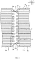
- the solar cell string 10 includes a plurality of solar cells 20 arranged in a first direction (the x-direction). Each of the solar cells 20 has a photoelectric conversion unit 23.
- the photoelectric conversion unit 23 generates carriers such as electrons or holes when light is received.
- the photoelectric conversion unit 23 may include a semiconductor substrate having one type of conductivity, a first semiconductor layer having the other type of conductivity arranged on a portion of the surface of the semiconductor substrate, and a second semiconductor layer having the one type of conductivity arranged on at least a portion of the surface of the semiconductor substrate in which the first semiconductor layer has not been arranged.
- a substantially intrinsic i-type semiconductor layer may be arranged between each of the first and second semiconductor layers and the semiconductor substrate.
- the photoelectric conversion unit 23 may include a semiconductor substrate having the one type of conductivity and provided with a p-type dopant diffusion area and an n-type dopant diffusion area.
- the first and second electrodes 21, 22 are arranged on the photoelectric conversion unit 23. More specifically, each of the first and second electrodes 21, 22 is arranged on the same main surface 23a of the photoelectric conversion unit 23. More specifically, the main surface 23a of the photoelectric conversion unit 23 includes a p-type surface and an n-type surface. The first electrode 21 is arranged on one of the p-type and n-type surfaces, and the second electrode 22 is arranged on the other surface.
- Each of the first and second electrodes 21, 22 are comb-shaped. Each of the first and second electrodes 21, 22 have a plurality of finger portions 21a, 22a and busbar portions 21b, 22b. Each of the finger portions 21a, 22a extends in the first direction (the x-direction). The finger portions 21a, 22a are interdigitated at intervals in a second direction (the y-direction) perpendicular to the first direction (x-direction).
- the finger portions 21a are connected electrically to the busbar portion 21b.
- the busbar portion 21b is arranged on one side of the finger portions 21a in the x-direction.
- the busbar portion 21b is arranged on one end of the solar cells 20 in the x-direction from one end in the y-direction to the other end in the y-direction.
- the busbar portion 21b has a first busbar portion 21b-1 and a second busbar portion 21b-2. The configuration will be explained in greater detail below.
- the plurality of finger portions 22a is connected electrically to the busbar portion 22b.
- the busbar portion 22b is arranged on the other side of the finger portions 22a in the x-direction.
- the busbar portion 22b is arranged on one end of the solar cells 20 in the x-direction from one end in the y-direction to the other end in the y-direction.
- the busbar portion 22b has a third busbar portion 22b-1 and a fourth busbar portion 22b-2. The configuration thereof will be explained in greater detail below.
- the plurality of solar cells 20 is connected electrically by means of a wiring member 30. More specifically, between solar cells 20 adjacent to each other in the first direction (the x-direction), the first electrode 21 of one of the solar cells 20 is connected electrically to the second electrode 22 of the other solar cell by means of a wiring member 30.
- the wiring member 30 and the solar cells 20 are bonded by means of the adhesive layer 40 shown in FIG. 5 .
- the adhesive layer 40 may include a cured resin adhesive.
- the adhesive layer 40 may constitute a cured resin adhesive, or may include a cured resin adhesive throughout which conductive particles have been dispersed.
- the wiring member 30 has an insulating substrate 31 and wiring 32 provided in the insulating substrate 31. Between solar cells 20 adjacent to each other in the first direction (the x-direction), the wiring 32 electrically connects the first electrode 21 of one of the solar cells 20 to the second electrode 22 of the other solar cell. In the example explained herein, the wiring 32 is provided on the main surface of the insulating substrate 31 on the side with the solar cells 20. However, some of the wiring 32 may be provided inside the insulating substrate 31.
- the insulating substrate 31 may be flexible.
- the insulating substrate 31 can be made from an insulating material such as a resin or a ceramic.
- the wiring 32 can be made of a metal such as Cu, Al or Ag, or an alloy including at least one of these metals.
- the wiring 32 has an adherend portion 32a bonded to the solar cells 20 by the adhesive layer 40.
- the adherend portion 32a is provided over the finger portions 21a, 22a and over the photoelectric conversion unit 23 where the finger portions 21a, 22a are not provided. This increases the adhesive force of the adherend portion 32a to the solar cells 20 due to an anchoring effect. This makes the wiring 30 less likely to peel off the solar cells 20. As a result, greater reliability can be realized. It is not necessary for all of the adherend portions 32a to be provided over the finger portions 21a, 22a and over the photoelectric conversion unit 23 where the finger portions 21a, 22a are not provided.
- Busbar portion 21b has a first busbar portion 21b-1 and a second busbar portion 21b-2.
- the boundary between the first busbar portion 21b-1 and the second busbar portion 21b-2 is denoted by a broken line.
- the first busbar portion 21b-1 and the second busbar portion 21b-2 are formed continuously.
- the first busbar portion 21b-1 is arranged in the central portion in the y-direction, which is the direction of extension of the busbar portion 21b.
- the second busbar portion 21b-2 is arranged on both ends in the y-direction. In other words, the second busbar portion 21b-2 is arranged to the outside of the first busbar portion 21b-1 in the y-direction, which is the direction of extension of the first busbar portion 21b-1.
- the second busbar portion 21b-2 is connected electrically to at least one of the finger portions 21a among the finger portions 21a arranged on an end in the y-direction.
- the second busbar portion 21b-2 is connected electrically to the adherend portions 32a of the wiring 32 and to inclined portions 32b in the y-direction among the adherend portions 32a of the wiring 32.
- the second busbar portion 21b-2 collects current from at least one finger portion 21a among the finger portions 21a arranged on the end in the y-direction.
- the first busbar portion 21b-1 is connected electrically to a finger portion 21a among the finger portions 21a positioned in the central portion in the y-direction not connected to the second busbar portion 21b-2.
- the electrical resistance of the first busbar portion 21b-1 is higher than the electrical resistance of the second busbar portion 21b-2.
- the thickness of the first busbar portion 21b-1 is equal to the thickness of the second busbar portion 21b-2, but the width of the first busbar portion 21b-1 is less than the width of the second busbar portion 21b-2.
- the width of the first busbar portion 21b-1 is nearly the same as the finger portions 21a.
- the edge of an inclined portion 32b positioned on the edge of the adherend portions 32a in the y-direction is inclined in the x-direction.
- the third busbar portion 22b-1 and the fourth busbar portion 22b-2 have the same configuration as the first busbar portion 21b-1 and the second busbar portion 21b-2.
- the modified example does not have the first busbar portion 21b-1 and third busbar portion 22b-1 shown in FIG. 6 , but does have a second busbar portion 21b-2 and a fourth busbar portion 22b-2.
- busbar portions are not provided on the periphery of the long sides facing adjacent solar cells 20, but can be provided on the periphery of the short sides.
- the finger portions 21a, 22a adjacent to the second busbar portion 21b-2 and the fourth busbar portion 22b-2 are connected to busbar portions 21b, 22b, but the other finger portions are not connected to busbar portions 21b, 22b. Even so, the effects are similar to those of the embodiment described above.
- first and second electrodes 21, 22 busbarless electrodes As in the modified example, loss due to recombination of carriers, especially loss due to recombination of minority carriers, can be suppressed. As a result, improved photoelectric conversion efficiency can be obtained.
Landscapes
- Engineering & Computer Science (AREA)
- Physics & Mathematics (AREA)
- Condensed Matter Physics & Semiconductors (AREA)
- Electromagnetism (AREA)
- General Physics & Mathematics (AREA)
- Computer Hardware Design (AREA)
- Microelectronics & Electronic Packaging (AREA)
- Power Engineering (AREA)
- Life Sciences & Earth Sciences (AREA)
- Sustainable Development (AREA)
- Sustainable Energy (AREA)
- Photovoltaic Devices (AREA)
Claims (4)
- Module solaire comprenant :une pluralité de piles solaires (20) ; etun câblage (32) connectant électriquement l'une des piles solaires (20) à une autre des piles solaires adjacentes à la pile solaire, dans lequelchacune des piles solaires (20) comprend :une unité de conversion photoélectrique (23) ; etune première électrode (21) et une deuxième électrode (22) agencées sur l'unité de conversion photoélectrique (23) et connectées à un câblage (32) via une couche adhésive (40) ;la première électrode (21) ayant une pluralité de portions de doigt (21a) et une portion de barre omnibus (21b) comportant une première portion de barre omnibus (21b-1) linéaire connectée électriquement à au moins l'une de la pluralité de portions de doigt (21a) de la première électrode (21) et une deuxième portion de barre omnibus (21b-2) connectée électriquement aux portions de doigt, parmi la pluralité de portions de doigt (21a) de la première électrode (21), qui ne sont pas connectées à la première portion de barre omnibus (21b-1), la deuxième portion de barre omnibus (21b-2) étant agencée à l'extérieur de la première portion de barre omnibus (21b-1) dans une direction d'extension de la première portion de barre omnibus (21b-1),la deuxième électrode (22) ayant une pluralité de portions de doigt (22a) et une portion de barre omnibus (22b) comportant une troisième portion de barre omnibus (22b-1) linéaire connectée électriquement à au moins l'une de la pluralité de portions de doigt (22a) de la deuxième électrode (22) et une quatrième portion de barre omnibus (22b-2) connectée électriquement aux portions de doigt, parmi la pluralité de portions de doigt (22a) de la deuxième électrode (22), qui ne sont pas connectées à la troisième portion de barre omnibus (22b-1), la quatrième portion de barre omnibus (22b-2) étant agencée à l'extérieur de la troisième portion de barre omnibus (22b-1) dans une direction d'extension de la troisième portion de barre omnibus (22b-1),dans lequella résistance électrique de la première portion de barre omnibus (21b-1) est supérieure à la résistance électrique de la deuxième portion de barre omnibus (21b-2), etchacune de la portion de barre omnibus (21b) de la première électrode (21) d'une pile solaire et de la portion de barre omnibus (22b) de la deuxième électrode (22) de l'autre pile solaire a une zone couverte par le câblage (32) et une zone non couverte par le câblage (32).
- Module solaire selon la revendication 1,
dans lequel la largeur de la première portion de barre omnibus (21b-1) dans une direction longitudinale de la pluralité de portions de doigt (21a) de la première électrode (21) est inférieure à la largeur de la deuxième portion de barre omnibus (21b-2) dans la direction longitudinale de la pluralité de portions de doigt (21a) de la première électrode (21), et
la largeur de la troisième portion de barre omnibus (22b-1) dans une direction longitudinale de la pluralité de portions de doigt (22a) de la deuxième électrode (22) est inférieure à la largeur de la quatrième portion de barre omnibus (22b-2) dans la direction longitudinale de la pluralité de portions de doigt (22a) de la deuxième électrode (22). - Module solaire selon la revendication 1, dans lequel la couche adhésive (40) comporte un adhésif en résine durcie dans laquelle des particules conductrices ont été dispersées.
- Module solaire selon la revendication 3, dans lequel le câblage (32) a une portion adhérente (32a) liée aux piles solaires (20) par la couche adhésive (40) de sorte que la portion adhérente (32a) soit prévue au-dessus des portions de doigt (21a, 22a) des première et deuxième électrodes (21, 22) et au-dessus de la section de l'unité de conversion photoélectrique (23) non pourvue de portions de doigt (21a, 22a) des première et deuxième électrodes (21, 22).
Applications Claiming Priority (2)
| Application Number | Priority Date | Filing Date | Title |
|---|---|---|---|
| JP2011148312 | 2011-07-04 | ||
| PCT/JP2012/062141 WO2013005475A1 (fr) | 2011-07-04 | 2012-05-11 | Module de cellules solaires et cellule solaire |
Publications (3)
| Publication Number | Publication Date |
|---|---|
| EP2731147A1 EP2731147A1 (fr) | 2014-05-14 |
| EP2731147A4 EP2731147A4 (fr) | 2015-04-01 |
| EP2731147B1 true EP2731147B1 (fr) | 2021-03-24 |
Family
ID=47436833
Family Applications (1)
| Application Number | Title | Priority Date | Filing Date |
|---|---|---|---|
| EP12808154.4A Withdrawn - After Issue EP2731147B1 (fr) | 2011-07-04 | 2012-05-11 | Module de cellules solaires |
Country Status (5)
| Country | Link |
|---|---|
| US (1) | US20140102508A1 (fr) |
| EP (1) | EP2731147B1 (fr) |
| JP (2) | JP6145884B2 (fr) |
| MY (1) | MY171640A (fr) |
| WO (1) | WO2013005475A1 (fr) |
Families Citing this family (10)
| Publication number | Priority date | Publication date | Assignee | Title |
|---|---|---|---|---|
| EP2819250B1 (fr) | 2013-06-26 | 2022-07-27 | 3M Innovative Properties Company | Ensemble de câble et procédé de connexion d'un câble électrique avec une installation électrique d'un réseau électrique |
| KR102087156B1 (ko) * | 2013-07-09 | 2020-03-10 | 엘지전자 주식회사 | 태양전지 모듈 |
| KR102132940B1 (ko) | 2013-11-29 | 2020-07-10 | 엘지전자 주식회사 | 태양 전지 및 그 제조 방법 |
| WO2015115566A1 (fr) * | 2014-01-31 | 2015-08-06 | 日立化成株式会社 | Ensemble de connexion d'électrodes, procédé de fabrication d'une cellule photovoltaïque, cellule photovoltaïque et module de cellule photovoltaïque |
| WO2015145885A1 (fr) | 2014-03-24 | 2015-10-01 | パナソニックIpマネジメント株式会社 | Module de cellule solaire, et cellule solaire |
| US9496437B2 (en) | 2014-03-28 | 2016-11-15 | Sunpower Corporation | Solar cell having a plurality of sub-cells coupled by a metallization structure |
| US11811360B2 (en) * | 2014-03-28 | 2023-11-07 | Maxeon Solar Pte. Ltd. | High voltage solar modules |
| US10770610B2 (en) | 2015-12-08 | 2020-09-08 | Sunpower Corporation | Photovoltaic module interconnect joints |
| KR101824523B1 (ko) * | 2017-01-11 | 2018-02-01 | 엘지전자 주식회사 | 태양 전지 모듈 및 이를 구비하는 휴대용 충전기 |
| WO2021232715A1 (fr) * | 2020-05-21 | 2021-11-25 | 晶澳太阳能有限公司 | Module de cellule solaire à contact arrière et procédé de préparation |
Family Cites Families (24)
| Publication number | Priority date | Publication date | Assignee | Title |
|---|---|---|---|---|
| JP2000164901A (ja) * | 1998-11-27 | 2000-06-16 | Kyocera Corp | 太陽電池 |
| US20050022857A1 (en) * | 2003-08-01 | 2005-02-03 | Daroczi Shandor G. | Solar cell interconnect structure |
| US7390961B2 (en) * | 2004-06-04 | 2008-06-24 | Sunpower Corporation | Interconnection of solar cells in a solar cell module |
| US7432596B1 (en) * | 2004-10-12 | 2008-10-07 | Energy Innovations, Inc. | Apparatus and method for bonding silicon wafer to conductive substrate |
| US7858875B2 (en) * | 2005-09-29 | 2010-12-28 | Enfocus Engineering Corp. | Radiant energy conversion system |
| JP2007103473A (ja) * | 2005-09-30 | 2007-04-19 | Sanyo Electric Co Ltd | 太陽電池装置および太陽電池モジュール |
| JP2007281044A (ja) * | 2006-04-04 | 2007-10-25 | Canon Inc | 太陽電池 |
| JP5230089B2 (ja) * | 2006-09-28 | 2013-07-10 | 三洋電機株式会社 | 太陽電池モジュール |
| WO2008080160A1 (fr) * | 2006-12-22 | 2008-07-03 | Advent Solar, Inc. | Technologies d'interconnexion pour cellules et modules solaires à contact arrière |
| DE102007003682A1 (de) * | 2007-01-25 | 2008-08-07 | Institut Für Solarenergieforschung Gmbh | Verschaltung von Rückseitenkontaktsolarzellen mit Lötstoplack und Metalldrähten |
| US20110120530A1 (en) * | 2007-08-23 | 2011-05-26 | Takayuki Isaka | Back surface contact type solar cell, back surface contact type solar cell with wiring board, solar cell string, and solar cell module |
| JP2009176782A (ja) * | 2008-01-21 | 2009-08-06 | Sanyo Electric Co Ltd | 太陽電池モジュール |
| JP5230222B2 (ja) * | 2008-02-21 | 2013-07-10 | 三洋電機株式会社 | 太陽電池 |
| KR101195624B1 (ko) * | 2008-03-31 | 2012-10-30 | 샤프 가부시키가이샤 | 태양 전지, 태양 전지 스트링 및 태양 전지 모듈 |
| JP4948473B2 (ja) | 2008-04-21 | 2012-06-06 | 三洋電機株式会社 | 太陽電池モジュール |
| US7915522B2 (en) * | 2008-05-30 | 2011-03-29 | Twin Creeks Technologies, Inc. | Asymmetric surface texturing for use in a photovoltaic cell and method of making |
| CN102132420A (zh) * | 2008-08-22 | 2011-07-20 | 三洋电机株式会社 | 太阳能电池模块、太阳能电池和太阳能电池模块的制造方法 |
| WO2010094010A2 (fr) * | 2009-02-13 | 2010-08-19 | Applied Materials, Inc. | Modules photovoltaïques à profil plat et faible concentration |
| CN102362363A (zh) * | 2009-03-23 | 2012-02-22 | 夏普株式会社 | 附配线基板的太阳能电池单元、太阳能电池组件及附配线基板的太阳能电池单元的制造方法 |
| JP2011009460A (ja) * | 2009-06-25 | 2011-01-13 | Kyocera Corp | 太陽電池モジュールの製造方法及び太陽電池モジュールの製造装置 |
| JP2011054721A (ja) * | 2009-09-01 | 2011-03-17 | Sharp Corp | 被接合部材の接合方法および接合構造体 |
| KR101130197B1 (ko) * | 2009-09-28 | 2012-03-30 | 엘지전자 주식회사 | 태양전지 모듈 및 그 제조 방법 |
| JP2011108969A (ja) * | 2009-11-20 | 2011-06-02 | Hitachi Cable Ltd | 太陽電池モジュールの製造方法、及び太陽電池用配線基板 |
| US8691694B2 (en) * | 2009-12-22 | 2014-04-08 | Henry Hieslmair | Solderless back contact solar cell module assembly process |
-
2012
- 2012-05-11 WO PCT/JP2012/062141 patent/WO2013005475A1/fr active Application Filing
- 2012-05-11 EP EP12808154.4A patent/EP2731147B1/fr not_active Withdrawn - After Issue
- 2012-05-11 JP JP2013522518A patent/JP6145884B2/ja not_active Expired - Fee Related
- 2012-05-11 MY MYPI2013702582A patent/MY171640A/en unknown
-
2013
- 2013-12-19 US US14/134,492 patent/US20140102508A1/en not_active Abandoned
-
2017
- 2017-04-27 JP JP2017088079A patent/JP2017126805A/ja active Pending
Non-Patent Citations (1)
| Title |
|---|
| None * |
Also Published As
| Publication number | Publication date |
|---|---|
| JP6145884B2 (ja) | 2017-06-14 |
| US20140102508A1 (en) | 2014-04-17 |
| EP2731147A4 (fr) | 2015-04-01 |
| WO2013005475A1 (fr) | 2013-01-10 |
| JPWO2013005475A1 (ja) | 2015-02-23 |
| JP2017126805A (ja) | 2017-07-20 |
| MY171640A (en) | 2019-10-22 |
| EP2731147A1 (fr) | 2014-05-14 |
Similar Documents
| Publication | Publication Date | Title |
|---|---|---|
| EP2731147B1 (fr) | Module de cellules solaires | |
| US9349897B2 (en) | Solar cell module and manufacturing method therefor | |
| JP5687506B2 (ja) | 太陽電池及び太陽電池モジュール | |
| EP2575183B1 (fr) | Module de cellule solaire | |
| EP2669954B1 (fr) | Cellule solaire et module de cellule solaire | |
| JP7291715B2 (ja) | 太陽電池デバイスおよび太陽電池モジュール | |
| WO2012117765A1 (fr) | Module de cellules solaires | |
| JP7530221B2 (ja) | 太陽電池ストリング及び太陽電池モジュール | |
| US9166088B2 (en) | Solar module | |
| US9373738B2 (en) | Solar module | |
| US10147831B2 (en) | Solar module and manufacturing method therefor | |
| WO2013042417A1 (fr) | Module de cellules solaires et cellule solaire | |
| JP5906422B2 (ja) | 太陽電池及び太陽電池モジュール | |
| JP7482708B2 (ja) | 太陽電池セル及び太陽電池モジュール | |
| JP2022149039A (ja) | 太陽電池モジュール | |
| JP6048837B2 (ja) | 太陽電池モジュール |
Legal Events
| Date | Code | Title | Description |
|---|---|---|---|
| PUAI | Public reference made under article 153(3) epc to a published international application that has entered the european phase |
Free format text: ORIGINAL CODE: 0009012 |
|
| 17P | Request for examination filed |
Effective date: 20140128 |
|
| AK | Designated contracting states |
Kind code of ref document: A1 Designated state(s): AL AT BE BG CH CY CZ DE DK EE ES FI FR GB GR HR HU IE IS IT LI LT LU LV MC MK MT NL NO PL PT RO RS SE SI SK SM TR |
|
| DAX | Request for extension of the european patent (deleted) | ||
| RA4 | Supplementary search report drawn up and despatched (corrected) |
Effective date: 20150304 |
|
| RIC1 | Information provided on ipc code assigned before grant |
Ipc: H01L 31/048 20140101AFI20150226BHEP Ipc: H01L 31/05 20140101ALI20150226BHEP |
|
| RAP1 | Party data changed (applicant data changed or rights of an application transferred) |
Owner name: PANASONIC INTELLECTUAL PROPERTY MANAGEMENT CO., LT |
|
| 17Q | First examination report despatched |
Effective date: 20170925 |
|
| REG | Reference to a national code |
Ref country code: DE Ref legal event code: R079 Ref document number: 602012074920 Country of ref document: DE Free format text: PREVIOUS MAIN CLASS: H01L0031040000 Ipc: H01L0031020000 |
|
| RIC1 | Information provided on ipc code assigned before grant |
Ipc: H01L 31/05 20140101ALI20201022BHEP Ipc: H01L 31/048 20140101ALI20201022BHEP Ipc: H01L 31/02 20060101AFI20201022BHEP |
|
| GRAP | Despatch of communication of intention to grant a patent |
Free format text: ORIGINAL CODE: EPIDOSNIGR1 |
|
| STAA | Information on the status of an ep patent application or granted ep patent |
Free format text: STATUS: GRANT OF PATENT IS INTENDED |
|
| INTG | Intention to grant announced |
Effective date: 20201222 |
|
| GRAS | Grant fee paid |
Free format text: ORIGINAL CODE: EPIDOSNIGR3 |
|
| GRAA | (expected) grant |
Free format text: ORIGINAL CODE: 0009210 |
|
| PUAC | Information related to the publication of a b1 document modified or deleted |
Free format text: ORIGINAL CODE: 0009299EPPU |
|
| AK | Designated contracting states |
Kind code of ref document: B1 Designated state(s): AL AT BE BG CH CY CZ DE DK EE ES FI FR GB GR HR HU IE IS IT LI LT LU LV MC MK MT NL NO PL PT RO RS SE SI SK SM TR |
|
| REG | Reference to a national code |
Ref country code: GB Ref legal event code: FG4D |
|
| STAA | Information on the status of an ep patent application or granted ep patent |
Free format text: STATUS: THE APPLICATION HAS BEEN WITHDRAWN |
|
| REG | Reference to a national code |
Ref country code: CH Ref legal event code: EP Ref country code: CH Ref legal event code: PK Free format text: DIE ERTEILUNG WURDE VOM EPA WIDERRUFEN. |
|
| REG | Reference to a national code |
Ref country code: DE Ref legal event code: R096 Ref document number: 602012074920 Country of ref document: DE |
|
| REG | Reference to a national code |
Ref country code: IE Ref legal event code: FG4D |
|
| REG | Reference to a national code |
Ref country code: AT Ref legal event code: REF Ref document number: 1375384 Country of ref document: AT Kind code of ref document: T Effective date: 20210415 |
|
| DB1 | Publication of patent cancelled |
Effective date: 20210319 |
|
| 18W | Application withdrawn |
Effective date: 20210315 |
|
| REG | Reference to a national code |
Ref country code: LU Ref legal event code: HK Effective date: 20210414 |
|
| REG | Reference to a national code |
Ref country code: DE Ref legal event code: R107 Ref document number: 602012074920 Country of ref document: DE |
|
| REG | Reference to a national code |
Ref country code: AT Ref legal event code: REZ Ref document number: 1375384 Country of ref document: AT Kind code of ref document: T Effective date: 20210324 |