EP2730002B1 - Dispositif pour régulation de champ électrique - Google Patents
Dispositif pour régulation de champ électrique Download PDFInfo
- Publication number
- EP2730002B1 EP2730002B1 EP12737511.1A EP12737511A EP2730002B1 EP 2730002 B1 EP2730002 B1 EP 2730002B1 EP 12737511 A EP12737511 A EP 12737511A EP 2730002 B1 EP2730002 B1 EP 2730002B1
- Authority
- EP
- European Patent Office
- Prior art keywords
- high voltage
- layer
- section
- resistive
- voltage component
- Prior art date
- Legal status (The legal status is an assumption and is not a legal conclusion. Google has not performed a legal analysis and makes no representation as to the accuracy of the status listed.)
- Active
Links
- 230000005684 electric field Effects 0.000 title claims description 53
- 230000003247 decreasing effect Effects 0.000 claims description 8
- 230000003292 diminished effect Effects 0.000 claims description 2
- 239000004020 conductor Substances 0.000 description 7
- 239000000463 material Substances 0.000 description 7
- 230000000052 comparative effect Effects 0.000 description 6
- 238000004519 manufacturing process Methods 0.000 description 6
- 238000009413 insulation Methods 0.000 description 5
- 239000012212 insulator Substances 0.000 description 4
- 238000009826 distribution Methods 0.000 description 2
- 230000014509 gene expression Effects 0.000 description 2
- 230000001052 transient effect Effects 0.000 description 2
- 230000000694 effects Effects 0.000 description 1
- 238000009434 installation Methods 0.000 description 1
- 238000012216 screening Methods 0.000 description 1
Images

Classifications
-
- H—ELECTRICITY
- H02—GENERATION; CONVERSION OR DISTRIBUTION OF ELECTRIC POWER
- H02G—INSTALLATION OF ELECTRIC CABLES OR LINES, OR OF COMBINED OPTICAL AND ELECTRIC CABLES OR LINES
- H02G15/00—Cable fittings
- H02G15/02—Cable terminations
- H02G15/06—Cable terminating boxes, frames or other structures
- H02G15/064—Cable terminating boxes, frames or other structures with devices for relieving electrical stress
- H02G15/068—Cable terminating boxes, frames or other structures with devices for relieving electrical stress connected to the cable shield only
-
- H—ELECTRICITY
- H02—GENERATION; CONVERSION OR DISTRIBUTION OF ELECTRIC POWER
- H02G—INSTALLATION OF ELECTRIC CABLES OR LINES, OR OF COMBINED OPTICAL AND ELECTRIC CABLES OR LINES
- H02G15/00—Cable fittings
- H02G15/08—Cable junctions
- H02G15/10—Cable junctions protected by boxes, e.g. by distribution, connection or junction boxes
- H02G15/103—Cable junctions protected by boxes, e.g. by distribution, connection or junction boxes with devices for relieving electrical stress
- H02G15/105—Cable junctions protected by boxes, e.g. by distribution, connection or junction boxes with devices for relieving electrical stress connected to the cable shield only
Definitions
- the present invention generally relates to electric field control.
- a device for controlling an electric field at a high voltage component comprising an inner deflector to be electrically connected to a live high voltage part of the high voltage component; a resistive layer adapted for field controlling purposes, to be arranged along the high voltage component, and which at one position is electrically connected to the inner deflector and at one end is adapted to be electrically connected to a grounded part of the high voltage component; an insulating layer arranged on the resistive layer and extending at least from the one position towards the one end of the resistive layer while ending without reaching the one end of the resistive layer; and a semi-conducting layer arranged on the insulating layer and extending at least from the one position towards the one end of the resistive layer and past the end of the insulating layer, thereby defining an outer triple point at the intersection of the resistive layer, the insulating layer, and the semi-conducting layer.
- a device of this type is known through for instance WO 00/74191 A1 .
- a device of this type is used for distributing the electric field where this is crucial and by that avoiding electric field concentrations and damaging of different type of equipment, such as cables.
- the electric potential between the live part and ground is distributed by means of a material with a suitable resistance forming the resistive layer.
- EP1870975 A discloses also a device of this type for controlling an electric field at a high voltage component, the device comprising a resistive layer for field control, an insulating layer arranged on the resistive layer and a semi-conducting or conducting layer arranged on the insulating layer.
- the three layers meet at a triple point, where the insulating layer ends.
- the interface between the resistive layer and the insulating layer makes in the triple point an angle to the semi-conducting or conducting layer of 60°-120°.
- WO 2008/076058 describes a field grading material and a device for grading an electric field at an interruption of the insulation layer arranged around a conductor in a cable.
- US 2003/188885 describes a cylindrical pre-molded rubber insulation tube.
- a rubber electrode layer is provided and used as a screening electrode to control the concentration of electric stress in insulator.
- HVDC High Voltage Direct Current
- the main challenge for DC equipment is the combined stress requirements of almost double nominal DC voltages and of DC voltages with superimposed transient voltages, like e.g. switching surges and lightning impulses.
- transient voltages like e.g. switching surges and lightning impulses.
- the conductivity of the material is the dominating parameters.
- transients additionally the permittivity needs to be taken into account.
- a worst case can be seen in the super position of a DC field and a fast transient of opposite polarity.
- extraordinary stress is achieved by superposition of space charge resistive and capacitive field distributions. This may lead to totally different stress distributions for transients and DC applied voltages, separately.
- the invention refers to a device for controlling an electric field at a high voltage component comprising an inner deflector electrically connected to a live high voltage part of the high voltage component; a resistive layer having a nonlinear current-voltage characteristic adapted for electrical field controlling purposes, and arranged along the high voltage component, and which at one position is electrically connected to the inner deflector and at one end is electrically connected to a grounded part of the high voltage component; an insulating layer arranged on the resistive layer and extending at least from the one position towards the one end of the resistive layer while ending, by a tapered field control geometry, without reaching the one end of the resistive layer; and a semi-conducting or conducting layer arranged on the insulating layer and extending at least from the one position towards the one end of the resistive layer and past the end of the insulating layer, thereby defining an outer triple point at the intersection of the resistive layer, the insulating layer, and the semi-conducting or conducting layer.
- the resistive layer which exhibits nonlinear current-voltage characteristics, has first, second, and third adjacent sections as seen from the one position towards the one end, wherein a portion of the first section extends below the inner deflector and is in contact with, and extend above, the inner deflector, and is located at an end of the inner deflector.
- the second section has, in a part thereof, a field control geometry with a gradually increasing thickness in the direction towards the outer triple point.
- the third section is extending from the outer triple point to an end of the resistive field grading layer.
- the electric field control device may comprise a connector, via which the inner deflector is electrically connected to the live high voltage part of the high voltage component, wherein the portion of the first section, which extends below the inner deflector, may be in contact with the connector only, with the inner deflector only, or with both the connector and the inner deflector.
- the portion of the first section, which extends below the inner deflector may extend under the inner deflector, a considerable distance, such as e.g. at least under 10, 20, 30, or 40 % of the extension of the inner deflector.
- the portion of the third section, in which the thickness is gradually decreasing in the direction towards the one end, may extend along a major part of the third section.
- the rate of the thickness decrease may decrease in the direction towards the one end.
- the above electric field control devices may be provided for controlling an electric field at a high voltage component, which is rated 300 kV or higher, or optionally 500 kV or higher, and which optionally is a DC high voltage component.
- the main tasks of the electric field control devices are for DC to provide interface grading and to avoid thermal runaway, for AC to keep the electric field below the bulk break down strength and the interface break down strength, and for transients of opposite polarity to keep the superimposed electric field below the bulk break down strength.
- the electric field control devices disclosed in this document lower electric fields in critical locations, increase the break down strength in critical locations, and lower the dissipated power in critical locations.
- the non-cylindrical shape of the resistive layer differs from the conventional cylindrical form, known in the prior art mentioned in the background section. This new shape gives reduced resistive losses of the resistive field grading layer and thereby limits the heat production that occurs.
- the resistive field grading layer can thereby be used for higher (DC) voltages without being damaged. Further, the resistive field grading layer is more cost-efficient than known such layers.
- Fig. 1 is a schematic cross-sectional view of a cable joint 12 provided with an electric field control device.
- the high voltage cable joint 12 comprises a high voltage cable consisting of a cable conductor 1, a cable insulator 2, and a semi-conducting ground layer 8, which are suitably prepared for the cable joint 12.
- a connector 3 is provided as a current connection device.
- the electric field control device comprises an inner deflector 4, a resistive field grading layer 5, an insulating layer 6, i.e. the joint insulation, and a semi-conducting layer 7, i.e. the mantle of the cable joint 12.
- the inner deflector 4 is electrically connected to the cable conductor 1 of the high-voltage cable via the connector 3 during installation of the cable joint 12. To this end, the connector 3 is electrically conductive.
- the inner deflector 4 is electrically semi-conducting.
- the semi-conducting layer 7, e.g. the mantle of the cable joint 12 and the semi-conducting ground layer 8 may instead be of an electrically conducting material.
- the resistive field grading layer 5 has nonlinear current-voltage characteristics and is adapted for field controlling purposes. During the fabrication of the cable joint 12, the resistive field grading layer 5 is arranged along the cable insulator 2 of the high-voltage cable and is at one end (to the right in Fig. 1 ) electrically connected to the semi-conducting ground layer 8 of the high-voltage cable. At one position (to the left in Fig. 1 ) the resistive field grading layer 5 is electrically connected to the inner deflector 4 and will hereby be electrically connected to the cable conductor 1 of the high-voltage cable.
- the insulating layer 6 is arranged on the resistive field grading layer 5 and extends at least from the one position and towards the one end of the resistive field grading layer 5 while ending, e.g. by tapered field control geometry, without reaching the one end of the resistive field grading layer 5.
- the semi-conducting layer 7 is arranged on the insulating layer 6 and extends at least from the one position and towards the one end of the resistive field grading layer 5 and past the end of the insulating layer 6.
- an outer triple point 11 can be defined at the intersection of the resistive field grading layer 5, the insulating layer 6, and the semi-conducting layer 7.
- the semi-conducting ground layer 8 of the high-voltage cable may be electrically connected to the semi-conducting layer 7, e.g. at the right hand of Fig. 1 .
- the resistive field grading layer 5 has first 5a, second 5b, and third 5c adjacent sections as seen from the one position towards the one end of the resistive field grading layer 5 (from left to right in Fig. 1 ), wherein the third section 5c is extending from the outer triple point 11 to the one end of the resistive field grading layer 5.
- a portion of the first section 5a of the resistive field grading layer 5 is in contact with, and extends below, the inner deflector 4 as can be seen in Fig. 1 .
- the portion of the first section 5a, which extends below the inner deflector 4, is in this embodiment, however, not extending so long that it will come into contact with the connector 3.
- FIG. 1 another portion of the first section 5a of the resistive field grading layer 5 is in contact with, and extends above, the inner deflector 4.
- the geometry of the resistive field grading layer 5 effectively prevents a superimposed field due to a DC field and transients of opposite polarity from becoming too high.
- the high voltage cable and the electric field control device may be cylinder symmetrical devices with a rotational symmetry axis 10 in a longitudinal direction.
- Each of the components of the high voltage cable and the electric field control device are rotation symmetric around the longitudinal symmetry axis 10.
- a mirror symmetry plane 9 in a radial direction i.e. the normal vector of the plane is extending in an axial direction
- the components of the high voltage cable and the electric field control device are mirrored to obtain the second high voltage cable of the cable joint 12 (to the left of the radial symmetry plane 9) and the components of the electric field control device, which are connected to that high voltage cable during fabrication of the cable joint 12.
- expressions such as a position, an end, and adjacent may be understood as a longitudinal position, a longitudinal end, and adjacent in the longitudinal direction.
- the inner deflector 4 is electrically connected to the cable conductor of the second high-voltage cable via the connector 3
- the resistive field grading layer 5 is arranged along the cable insulator of the second high-voltage cable and is at a second end electrically connected to the semi-conducting ground layer of the second high-voltage cable.
- the resistive field grading layer 5 is electrically connected to the inner deflector 4 and will hereby be connected to the cable conductor 1 of the high-voltage cable.
- the insulating layer 6 is arranged on the resistive field grading layer 5 and extends at least from the second position and towards the second end of the resistive field grading layer 5 while ending, e.g. by tapered field control geometry, without reaching the second end of the resistive field grading layer 5.
- the semi-conducting layer 7 is arranged on the insulating layer 6 and extends at least from the second position and towards the second end of the resistive field grading layer 5 and past the end of the insulating layer 6, which does not reach the second end of the resistive field grading layer 5.
- a second outer triple point can be defined at the intersection of the resistive field grading layer 5, the insulating layer 6, and the semi-conducting layer 7 at the second high voltage cable.
- the resistive field grading layer 5 has fourth, fifth, and sixth adjacent sections as seen from the second position and towards the second end of the resistive field grading layer 5 (not illustrated), wherein a portion of the fourth section is in contact with, and extends below, the inner deflector 4.
- the second section 5b of the resistive field grading layer 5 has a tapered field control geometry with a gradually increasing thickness in the direction towards the outer triple point 11, whereas the first section 5a of the resistive field grading layer 5 may be a thin uniform layer of a substantially constant thickness.
- the gradually increasing thickness in the direction towards the outer triple point 11 may exist in the entire or at least in a substantial part of the second section 5b of the resistive field grading layer 5.
- the resistive field grading layer 5 is locally diminished in the first section 5a and in the portion of the second section 5b closest to the first section 5a.
- the resistive losses of the resistive field grading layer 5 are lowered, thereby limiting the heat production.
- the third section 5c of the resistive field grading layer 5 may have, at least in a substantial portion thereof, a gradually decreasing thickness in the direction towards the one end of the resistive field grading layer 5.
- the portion of the third section 5c in which the thickness is gradually decreasing in the direction towards the one end of the resistive field grading layer 5, may extend along a major part of the third section 5c, preferably from the outer triple point 11 to a position where the end of the semi-conducting ground layer 8 of the high-voltage cable is located.
- the thickness decrease is preferably curved.
- Above the semi-conducting ground layer 8 of the high-voltage cable the thickness of the third section 5c is preferably constant, whereby the constant can as well become zero, i.e. the resistive layers vanishes in direction of the semi-conducting ground layer 8.
- the rate of the thickness decrease may be decreasing in the direction towards the one end. Also the higher derivatives of the thickness as a function of distance in the direction towards the one end may be negative.
- the thickness may increase from right to left approximately according to a polynomial.
- the distance between the outer triple point 11 and the semi-conducting ground layer 8 is increased, thereby influencing the axial electric field in the interfaces between the cable insulation 2 and the resistive field grading layer 5 and between the resistive field grading layer 5 and the joint insulation 6. It needs to extend a certain length in order to sufficiently distribute the electric field in the axial direction.
- first section 5a of the resistive field grading layer 5 may have a maximum thickness, which is smaller than a minimum thickness of the second section 5b of the resistive field grading layer 5, and the resistive field grading layer 5 may be thickest at the outer triple point 11.
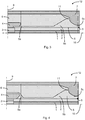
- Fig. 2 is a schematic cross-sectional view of a cable joint 12 provided with an electric field control device, which differs from the electric field control device of Fig. 1 in that the radially extending end side and the upper side of the inner deflector is not covered by the resistive field grading layer 5. Instead, the insulating layer 6 is in contact with, and extends at the radially extending end side and on top of, the inner deflector 4.
- the field grading material of the resistive field grading layer 5 introduces space charge fields. By means of omitting the resistive field grading layer 5 on top of the inner deflector, the space charge field at a critical location such as at the inner deflector 4 is decreased.
- Another alternative could be to provide an electric field control device, which differs from the electric field control device of Fig. 1 in that the radially extending end side and the upper side of the inner deflector is only partly covered by the resistive field grading layer 5, i.e. the resistive field grading layer 5 fade out on top of the inner deflector 4.
- Fig. 3 is a schematic cross-sectional view of a cable joint 12 provided with an electric field control device, which differs from the electric field control device of Fig. 2 in that the portion of the first section 5a of the resistive field grading layer 5, which extends below the inner deflector 4, is extending further to be in contact with, and arranged partly on top of, the connector 3.
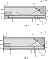
- Fig. 4 is a schematic cross-sectional view of a cable joint 12 provided with an electric field control device, which differs from the electric field control device of Fig. 1 in that a portion of the first section 5a of the resistive field grading layer 5 has a gradually increasing thickness in the direction towards the second section 5b, wherein this portion is located at an end of the inner deflector 4.
- a portion of the first section 5a of the resistive field grading layer 5 has a gradually increasing thickness in the direction towards the second section 5b, wherein this portion is located at an end of the inner deflector 4.
- Fig. 5 is a schematic cross-sectional view of a cable joint 12 provided with an electric field control device, which differs from the electric field control device of Fig. 1 in that a portion of the first section 5a of the resistive field grading layer 5 has a gradually increasing thickness in the direction towards the second section 5b, wherein this portion is located at a distance from the radially extending end side of the inner deflector 4 in the direction towards the second section 5b.
- the electric field control device of Fig. 5 is easier and simpler, and thus cheaper, to manufacture as compared to the other illustrated electric field control devices.
- Fig. 6 is a schematic cross-sectional view of a cable joint 12 provided with an electric field control device, which differs from the electric field control device of Fig. 1 in that both a portion of the first section 5a of the resistive field grading layer 5 and a portion of the insulating layer 6 extend below the inner deflector 4. The portion of the first section 5a of the resistive field grading layer 5 does not extend to the inner deflector is only in contact with the connector 3.
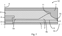
- Fig. 7 is a schematic cross-sectional view of a cable joint 12 provided with an electric field control device, which differs from the electric field control device of Fig. 6 in the portion of the first section 5a of the resistive field grading layer 5 extends to the inner deflector 4, and is thus in contact with the connector 3 and the inner deflector 4.
- the resistive layer 5 may instead extend between the connector 3 and the inner deflector 4 all the way to the mirror symmetry plane 9.
- the high voltage cable joints 12 may carry an alternating voltage or a direct voltage.
- the electric field control devices can be used at various high voltage components such as cable joints, cable terminations, and cable connections, but also as bushings in switchgears and vacuum breakers.
- high voltage components such as cable joints, cable terminations, and cable connections, but also as bushings in switchgears and vacuum breakers.
- no mirror symmetry as illustrated in the drawings is necessary. Axially, the entire device is illustrated in the drawings.
- the electric field control devices disclosed above may be provided for controlling an electric field at a high voltage component, which is rated 300 kV or higher, or optionally 500 kV or higher, and which optionally is a DC high voltage component.
Landscapes
- Emergency Protection Circuit Devices (AREA)
- Connector Housings Or Holding Contact Members (AREA)
- Cable Accessories (AREA)
- Insulation, Fastening Of Motor, Generator Windings (AREA)
- Electron Sources, Ion Sources (AREA)
- Gas-Insulated Switchgears (AREA)
Claims (13)
- Dispositif pour commander un champ électrique au niveau d'un composant de haute tension comprenant :- un déflecteur intérieur (4) relié électriquement à une partie de haute tension sous tension (1) du composant de haute tension ;- une couche résistive (5) ayant des caractéristiques de courant-tension non linéaires adaptées à des fins de commande de champ électrique, et agencée le long dudit composant de haute tension, et qui, à une position, est reliée au déflecteur intérieur (4) et, à une extrémité, est reliée électriquement à une partie mise à la masse (8) du composant de haute tension ;- une couche isolante (6) agencée sur ladite couche résistive (5) et s'étendant au moins depuis ladite position vers ladite extrémité de la couche résistive (5) tout en se terminant sans atteindre ladite extrémité de la couche résistive (5) ; et- une couche semiconductrice ou conductrice (7) agencée sur la couche isolante (6) et s'étendant au moins depuis ladite position vers ladite extrémité de la couche résistive (5) et au-delà de l'extrémité de la couche isolante (6), en définissant de ce fait un point triple extérieur (11) à l'intersection de la couche résistive (5), la couche isolante (6) et la couche semiconductrice ou conductrice (7),caractérisé en ce que- la couche résistive (5) a des première, deuxième et troisième sections adjacentes (5a, 5b, 5c) en vue depuis ladite position vers ladite extrémité, dans lequel- une portion de la première section (5a) s'étend au-dessous dudit déflecteur intérieur (4) et est en contact avec le, et s'étend au-dessus du, déflecteur intérieur (4), et est située à une extrémité du déflecteur intérieur (4),- la deuxième section (5b) a, dans une partie de celle-ci, une épaisseur progressivement croissante dans la direction vers le point triple extérieur (11), et- la troisième section (5c) s'étend depuis le point triple extérieur (11) jusqu'à une extrémité de la couche résistive de gradation de champ (5).
- Dispositif selon la revendication 1, comprenant un connecteur (3), par l'intermédiaire duquel ledit déflecteur intérieur (4) est relié électriquement à ladite partie de haute tension sous tension (1) du composant de haute tension.
- Dispositif selon la revendication 2, dans lequel ladite portion de la première section (5a), qui s'étend au-dessous dudit déflecteur intérieur (4), est en contact uniquement avec ledit déflecteur intérieur (4), ou avec à la fois le connecteur (3) et le déflecteur intérieur (4) .
- Dispositif selon l'une quelconque des revendications 1 à 3, dans lequel une portion de la première section (5a) a une épaisseur progressivement croissante dans la direction vers la deuxième section (5b).
- Dispositif selon l'une quelconque des revendications 1 à 4, dans lequel la troisième section (5c) a, au moins dans une portion substantielle de celle-ci, une épaisseur progressivement décroissante dans la direction vers ladite extrémité.
- Dispositif selon la revendication 5, dans lequel la portion de la troisième section (5c), dans laquelle l'épaisseur est progressivement décroissante dans la direction vers ladite extrémité, s'étend depuis le point triple extérieur jusqu'à l'extrémité d'une partie de masse (8) du composant de haute tension.
- Dispositif selon la revendication 5 ou 6, dans lequel le taux de la diminution d'épaisseur diminue dans la direction vers ladite extrémité.
- Dispositif selon l'une quelconque des revendications 1 à 7, dans lequel la couche résistive (5) est la plus épaisse au niveau du point triple extérieur (11).
- Dispositif selon l'une quelconque des revendications 1 à 8, dans lequel- ledit dispositif est agencé pour commander un champ électrique au niveau d'un autre composant de haute tension ;- ledit déflecteur intérieur (4) est relié électriquement à une partie de haute tension sous tension de l'autre composant de haute tension ;- ladite couche résistive (5) est agencée le long dudit autre composant de haute tension et, à une autre position, est reliée électriquement à ladite partie de haute tension sous tension de l'autre composant de haute tension et, à une autre extrémité, est apte à être reliée électriquement à une partie mise à la masse de l'autre composant de haute tension ;- ladite couche isolante (6) s'étend au moins depuis ladite autre position vers ladite autre extrémité de la couche résistive (5) tout en se terminant sans atteindre ladite autre extrémité de la couche résistive (5) ;- ladite couche semiconductrice ou conductrice (7) agencée sur la couche isolante (6) et s'étendant au moins depuis ladite autre position vers ladite autre extrémité de la couche résistive (5) et au-delà de l'extrémité de la couche isolante (6), en définissant de ce fait un autre point triple extérieur à une intersection de la couche résistive (5), la couche isolante (6) et la couche semiconductrice ou conductrice (7) ;- la couche résistive (5) a des quatrième, cinquième et sixième sections adjacentes en vue depuis ladite autre position vers ladite autre extrémité, dans lequel- une portion de la quatrième section s'étend au-dessous dudit déflecteur intérieur (4).
- Dispositif selon la revendication 9, dans lequel- le composant de haute tension et l'autre composant de haute tension sont chacun un câble de haute tension ; et- ledit dispositif est prévu pour raccorder les câbles de haute tension dans un raccord de câble.
- Dispositif selon l'une quelconque des revendications 1 à 10, dans lequel- le composant de haute tension est un câble de haute tension, un dispositif de commutation ou un casse-vide ; et- ledit dispositif est prévu pour terminer ledit câble de haute tension dans une terminaison de câble ou pour être utilisé en tant qu'un manchon.
- Dispositif selon l'une quelconque des revendications 1 à 11, dans lequel ledit dispositif est prévu pour commander un champ électrique au niveau d'un composant de haute tension, qui a une tension nominale supérieure ou égale à 300 kV, ou facultativement supérieure ou égale à 500 kV, et facultativement qui est un composant de haute tension CC.
- Dispositif selon l'une quelconque des revendications 1 à 12, dans lequel la couche résistive (5) est diminuée localement dans la première section (5a) et dans la portion de la deuxième section (5b) la plus proche de la première section (5a).
Applications Claiming Priority (2)
| Application Number | Priority Date | Filing Date | Title |
|---|---|---|---|
| US201161504342P | 2011-07-05 | 2011-07-05 | |
| PCT/EP2012/063041 WO2013004748A2 (fr) | 2011-07-05 | 2012-07-04 | Dispositif pour régulation de champ électrique |
Publications (2)
| Publication Number | Publication Date |
|---|---|
| EP2730002A2 EP2730002A2 (fr) | 2014-05-14 |
| EP2730002B1 true EP2730002B1 (fr) | 2021-07-28 |
Family
ID=46545753
Family Applications (1)
| Application Number | Title | Priority Date | Filing Date |
|---|---|---|---|
| EP12737511.1A Active EP2730002B1 (fr) | 2011-07-05 | 2012-07-04 | Dispositif pour régulation de champ électrique |
Country Status (8)
| Country | Link |
|---|---|
| US (1) | US9263875B2 (fr) |
| EP (1) | EP2730002B1 (fr) |
| JP (1) | JP5805865B2 (fr) |
| KR (1) | KR101578628B1 (fr) |
| CN (1) | CN103718404B (fr) |
| AU (1) | AU2012280287B9 (fr) |
| IN (1) | IN2014CN00774A (fr) |
| WO (1) | WO2013004748A2 (fr) |
Families Citing this family (15)
| Publication number | Priority date | Publication date | Assignee | Title |
|---|---|---|---|---|
| CN103718404B (zh) | 2011-07-05 | 2018-04-10 | Abb Hv电缆瑞士有限责任公司 | 用于电场控制的设备 |
| US9306340B2 (en) | 2013-12-13 | 2016-04-05 | General Electric Company | System and method for sub-sea cable termination |
| KR102238971B1 (ko) | 2014-02-21 | 2021-04-12 | 엘에스전선 주식회사 | Dc용 케이블의 종단접속함 |
| KR101860661B1 (ko) * | 2014-08-22 | 2018-05-23 | 엔케이티 에이치브이 케이블스 게엠베하 | 고전력 케이블용 전계 제어 디바이스 및 그 제조 방법 |
| CH710800B1 (de) * | 2015-08-27 | 2016-08-31 | Gramespacher Hansjörg | Vorgefertigter Muffenkörper für die Verbindung zweier Hochspannungspolymerkabel für Gleichstrom. |
| EP3516749B1 (fr) | 2016-09-19 | 2023-11-01 | Prysmian S.p.A. | Jonction pour câbles à courant continu à haute tension |
| US11476614B2 (en) | 2017-05-11 | 2022-10-18 | Prysmian S.P.A. | Cable termination system, termination assembly and method for installing such a termination assembly |
| CA3063008A1 (fr) * | 2017-05-11 | 2018-11-15 | Prysmian S.P.A. | Systeme de terminaisons de cable, ensemble de terminaisons et procede d'installation d'un tel ensemble de terminaisons |
| NO20170997A1 (en) | 2017-06-16 | 2018-11-26 | Benestad Solutions As | High voltage wet-mate connection assembly |
| CN110915087B (zh) * | 2017-07-13 | 2021-04-16 | 住友电气工业株式会社 | 非欧姆组合物及其制造方法、电缆中间连接单元以及电缆终端连接单元 |
| US11939461B2 (en) | 2019-01-18 | 2024-03-26 | Sumitomo Electric Industries, Ltd. | Non-ohmic composition, cable connection unit, and method for producing cable connection unit |
| CN113261068B (zh) * | 2019-01-18 | 2022-11-08 | 住友电气工业株式会社 | 非欧姆组合物、电缆连接用单元以及电缆连接用单元的制造方法 |
| EP4071358A4 (fr) * | 2019-12-04 | 2024-04-03 | Asahi Rubber Inc. | Corps collé constitué d'un objet à coller et d'un matériau de base fonctionnel |
| KR20230175125A (ko) * | 2022-06-21 | 2023-12-29 | 엘에스전선 주식회사 | 직류 전력케이블 시스템 |
| KR20230175124A (ko) * | 2022-06-21 | 2023-12-29 | 엘에스전선 주식회사 | 직류 전력케이블 시스템 |
Family Cites Families (9)
| Publication number | Priority date | Publication date | Assignee | Title |
|---|---|---|---|---|
| EP0491091A1 (fr) | 1990-12-19 | 1992-06-24 | Siemens Aktiengesellschaft | Câble haute-tension à isolation plastique à élément de commande coulissé là-dessus |
| JPH0731044A (ja) * | 1993-07-09 | 1995-01-31 | Fujikura Ltd | 絶縁性樹脂成形品 |
| SE514209C2 (sv) | 1999-05-28 | 2001-01-22 | Abb Ab | Styrning av elektriskt fält vid likspänning |
| TW588488B (en) * | 2001-11-27 | 2004-05-21 | Fujikura Ltd | Connecting structure for electrical connection power cable, connecting device and manufacturing method of connecting device |
| AU2002351802B2 (en) * | 2002-10-30 | 2007-10-25 | Prysmian Cavi E Sistemi Energia S.R.L. | Process for manufacturing the elastomeric sleeve of a joint for electrical cables and manufacturing apparatus thereof |
| JP4158904B2 (ja) * | 2003-04-18 | 2008-10-01 | 古河電気工業株式会社 | 常温収縮型ゴムユニット |
| ATE476775T1 (de) * | 2006-06-21 | 2010-08-15 | Abb Technology Ltd | Vorrichtung zur elektrischen feldsteuerung |
| SE531409C2 (sv) * | 2006-12-20 | 2009-03-24 | Abb Research Ltd | Fältstyrande material |
| CN103718404B (zh) | 2011-07-05 | 2018-04-10 | Abb Hv电缆瑞士有限责任公司 | 用于电场控制的设备 |
-
2012
- 2012-07-04 CN CN201280033327.8A patent/CN103718404B/zh not_active Expired - Fee Related
- 2012-07-04 JP JP2014517791A patent/JP5805865B2/ja active Active
- 2012-07-04 WO PCT/EP2012/063041 patent/WO2013004748A2/fr active Application Filing
- 2012-07-04 AU AU2012280287A patent/AU2012280287B9/en active Active
- 2012-07-04 EP EP12737511.1A patent/EP2730002B1/fr active Active
- 2012-07-04 KR KR1020147002740A patent/KR101578628B1/ko active IP Right Grant
- 2012-07-04 IN IN774CHN2014 patent/IN2014CN00774A/en unknown
-
2014
- 2014-01-06 US US14/148,347 patent/US9263875B2/en active Active
Non-Patent Citations (1)
| Title |
|---|
| None * |
Also Published As
| Publication number | Publication date |
|---|---|
| JP2014518500A (ja) | 2014-07-28 |
| AU2012280287B9 (en) | 2015-07-23 |
| AU2012280287A1 (en) | 2014-01-16 |
| IN2014CN00774A (fr) | 2015-04-03 |
| AU2012280287B2 (en) | 2015-07-16 |
| CN103718404B (zh) | 2018-04-10 |
| US20140116746A1 (en) | 2014-05-01 |
| WO2013004748A3 (fr) | 2013-11-07 |
| CN103718404A (zh) | 2014-04-09 |
| KR20140030330A (ko) | 2014-03-11 |
| KR101578628B1 (ko) | 2015-12-17 |
| JP5805865B2 (ja) | 2015-11-10 |
| US9263875B2 (en) | 2016-02-16 |
| EP2730002A2 (fr) | 2014-05-14 |
| WO2013004748A2 (fr) | 2013-01-10 |
Similar Documents
| Publication | Publication Date | Title |
|---|---|---|
| EP2730002B1 (fr) | Dispositif pour régulation de champ électrique | |
| EP1870975B1 (fr) | Dispositif de commande de champ électrique | |
| US10355470B2 (en) | Cable fitting for connecting a high-voltage cable to a high-voltage component | |
| EP2572422A2 (fr) | Appareil de terminaison de câble pour courant continu à haute tension | |
| JP2006296190A (ja) | Dc電気ケーブルの合成材料端部 | |
| SE514209C2 (sv) | Styrning av elektriskt fält vid likspänning | |
| CN105529617B (zh) | 一种线路避雷器 | |
| EP2572424A2 (fr) | Terminaison d'un câble haute tension à courant continu | |
| EP3516749B1 (fr) | Jonction pour câbles à courant continu à haute tension | |
| EP3622600B1 (fr) | Système de terminaisons de câble, ensemble de terminaisons et procédé d'installation d'un tel ensemble de terminaisons | |
| EP3933870A1 (fr) | Suppression des transitoires haute fréquence d'interrupteurs ht à résistance coulissante | |
| RU97013U1 (ru) | Соединительная муфта для силового кабеля | |
| AU2014383641B2 (en) | Power cable termination device for gas-insulated switchgear | |
| US11476614B2 (en) | Cable termination system, termination assembly and method for installing such a termination assembly | |
| CN205724824U (zh) | 应力控制体 | |
| JP4253404B2 (ja) | 高電圧機器用絶縁物 | |
| KR20190083504A (ko) | 전계 제어 디바이스 |
Legal Events
| Date | Code | Title | Description |
|---|---|---|---|
| PUAI | Public reference made under article 153(3) epc to a published international application that has entered the european phase |
Free format text: ORIGINAL CODE: 0009012 |
|
| 17P | Request for examination filed |
Effective date: 20140128 |
|
| AK | Designated contracting states |
Kind code of ref document: A2 Designated state(s): AL AT BE BG CH CY CZ DE DK EE ES FI FR GB GR HR HU IE IS IT LI LT LU LV MC MK MT NL NO PL PT RO RS SE SI SK SM TR |
|
| AX | Request for extension of the european patent |
Extension state: BA ME |
|
| R17P | Request for examination filed (corrected) |
Effective date: 20140507 |
|
| RBV | Designated contracting states (corrected) |
Designated state(s): AL AT BE BG CH CY CZ DE DK EE ES FI FR GB GR HR HU IE IS IT LI LT LU LV MC MK MT NL NO PL PT RO RS SE SI SK SM TR |
|
| DAX | Request for extension of the european patent (deleted) | ||
| RAP1 | Party data changed (applicant data changed or rights of an application transferred) |
Owner name: ABB HV CABLES (SWITZERLAND) GMBH |
|
| RAP1 | Party data changed (applicant data changed or rights of an application transferred) |
Owner name: NKT HV CABLES GMBH |
|
| STAA | Information on the status of an ep patent application or granted ep patent |
Free format text: STATUS: EXAMINATION IS IN PROGRESS |
|
| 17Q | First examination report despatched |
Effective date: 20191028 |
|
| RAP1 | Party data changed (applicant data changed or rights of an application transferred) |
Owner name: NKT HV CABLES AB |
|
| STAA | Information on the status of an ep patent application or granted ep patent |
Free format text: STATUS: EXAMINATION IS IN PROGRESS |
|
| GRAP | Despatch of communication of intention to grant a patent |
Free format text: ORIGINAL CODE: EPIDOSNIGR1 |
|
| STAA | Information on the status of an ep patent application or granted ep patent |
Free format text: STATUS: GRANT OF PATENT IS INTENDED |
|
| RIC1 | Information provided on ipc code assigned before grant |
Ipc: H02G 15/068 20060101AFI20210201BHEP Ipc: H02G 15/105 20060101ALI20210201BHEP |
|
| INTG | Intention to grant announced |
Effective date: 20210224 |
|
| GRAS | Grant fee paid |
Free format text: ORIGINAL CODE: EPIDOSNIGR3 |
|
| GRAA | (expected) grant |
Free format text: ORIGINAL CODE: 0009210 |
|
| STAA | Information on the status of an ep patent application or granted ep patent |
Free format text: STATUS: THE PATENT HAS BEEN GRANTED |
|
| AK | Designated contracting states |
Kind code of ref document: B1 Designated state(s): AL AT BE BG CH CY CZ DE DK EE ES FI FR GB GR HR HU IE IS IT LI LT LU LV MC MK MT NL NO PL PT RO RS SE SI SK SM TR |
|
| REG | Reference to a national code |
Ref country code: GB Ref legal event code: FG4D |
|
| RIN1 | Information on inventor provided before grant (corrected) |
Inventor name: RAPP, HANS Inventor name: MING, LI Inventor name: UNGE, MIKAEL Inventor name: GAEFVERT, UNO Inventor name: SALTZER, MARKUS |
|
| REG | Reference to a national code |
Ref country code: CH Ref legal event code: EP |
|
| REG | Reference to a national code |
Ref country code: AT Ref legal event code: REF Ref document number: 1415570 Country of ref document: AT Kind code of ref document: T Effective date: 20210815 |
|
| REG | Reference to a national code |
Ref country code: IE Ref legal event code: FG4D |
|
| REG | Reference to a national code |
Ref country code: DE Ref legal event code: R096 Ref document number: 602012076220 Country of ref document: DE |
|
| REG | Reference to a national code |
Ref country code: LT Ref legal event code: MG9D |
|
| REG | Reference to a national code |
Ref country code: NL Ref legal event code: FP |
|
| REG | Reference to a national code |
Ref country code: AT Ref legal event code: MK05 Ref document number: 1415570 Country of ref document: AT Kind code of ref document: T Effective date: 20210728 |
|
| PG25 | Lapsed in a contracting state [announced via postgrant information from national office to epo] |
Ref country code: AT Free format text: LAPSE BECAUSE OF FAILURE TO SUBMIT A TRANSLATION OF THE DESCRIPTION OR TO PAY THE FEE WITHIN THE PRESCRIBED TIME-LIMIT Effective date: 20210728 Ref country code: BG Free format text: LAPSE BECAUSE OF FAILURE TO SUBMIT A TRANSLATION OF THE DESCRIPTION OR TO PAY THE FEE WITHIN THE PRESCRIBED TIME-LIMIT Effective date: 20211028 Ref country code: LT Free format text: LAPSE BECAUSE OF FAILURE TO SUBMIT A TRANSLATION OF THE DESCRIPTION OR TO PAY THE FEE WITHIN THE PRESCRIBED TIME-LIMIT Effective date: 20210728 Ref country code: RS Free format text: LAPSE BECAUSE OF FAILURE TO SUBMIT A TRANSLATION OF THE DESCRIPTION OR TO PAY THE FEE WITHIN THE PRESCRIBED TIME-LIMIT Effective date: 20210728 Ref country code: NO Free format text: LAPSE BECAUSE OF FAILURE TO SUBMIT A TRANSLATION OF THE DESCRIPTION OR TO PAY THE FEE WITHIN THE PRESCRIBED TIME-LIMIT Effective date: 20211028 Ref country code: PT Free format text: LAPSE BECAUSE OF FAILURE TO SUBMIT A TRANSLATION OF THE DESCRIPTION OR TO PAY THE FEE WITHIN THE PRESCRIBED TIME-LIMIT Effective date: 20211129 Ref country code: ES Free format text: LAPSE BECAUSE OF FAILURE TO SUBMIT A TRANSLATION OF THE DESCRIPTION OR TO PAY THE FEE WITHIN THE PRESCRIBED TIME-LIMIT Effective date: 20210728 Ref country code: FI Free format text: LAPSE BECAUSE OF FAILURE TO SUBMIT A TRANSLATION OF THE DESCRIPTION OR TO PAY THE FEE WITHIN THE PRESCRIBED TIME-LIMIT Effective date: 20210728 Ref country code: HR Free format text: LAPSE BECAUSE OF FAILURE TO SUBMIT A TRANSLATION OF THE DESCRIPTION OR TO PAY THE FEE WITHIN THE PRESCRIBED TIME-LIMIT Effective date: 20210728 Ref country code: SE Free format text: LAPSE BECAUSE OF FAILURE TO SUBMIT A TRANSLATION OF THE DESCRIPTION OR TO PAY THE FEE WITHIN THE PRESCRIBED TIME-LIMIT Effective date: 20210728 |
|
| PG25 | Lapsed in a contracting state [announced via postgrant information from national office to epo] |
Ref country code: PL Free format text: LAPSE BECAUSE OF FAILURE TO SUBMIT A TRANSLATION OF THE DESCRIPTION OR TO PAY THE FEE WITHIN THE PRESCRIBED TIME-LIMIT Effective date: 20210728 Ref country code: LV Free format text: LAPSE BECAUSE OF FAILURE TO SUBMIT A TRANSLATION OF THE DESCRIPTION OR TO PAY THE FEE WITHIN THE PRESCRIBED TIME-LIMIT Effective date: 20210728 Ref country code: GR Free format text: LAPSE BECAUSE OF FAILURE TO SUBMIT A TRANSLATION OF THE DESCRIPTION OR TO PAY THE FEE WITHIN THE PRESCRIBED TIME-LIMIT Effective date: 20211029 |
|
| PG25 | Lapsed in a contracting state [announced via postgrant information from national office to epo] |
Ref country code: DK Free format text: LAPSE BECAUSE OF FAILURE TO SUBMIT A TRANSLATION OF THE DESCRIPTION OR TO PAY THE FEE WITHIN THE PRESCRIBED TIME-LIMIT Effective date: 20210728 |
|
| REG | Reference to a national code |
Ref country code: DE Ref legal event code: R097 Ref document number: 602012076220 Country of ref document: DE |
|
| PG25 | Lapsed in a contracting state [announced via postgrant information from national office to epo] |
Ref country code: SM Free format text: LAPSE BECAUSE OF FAILURE TO SUBMIT A TRANSLATION OF THE DESCRIPTION OR TO PAY THE FEE WITHIN THE PRESCRIBED TIME-LIMIT Effective date: 20210728 Ref country code: SK Free format text: LAPSE BECAUSE OF FAILURE TO SUBMIT A TRANSLATION OF THE DESCRIPTION OR TO PAY THE FEE WITHIN THE PRESCRIBED TIME-LIMIT Effective date: 20210728 Ref country code: RO Free format text: LAPSE BECAUSE OF FAILURE TO SUBMIT A TRANSLATION OF THE DESCRIPTION OR TO PAY THE FEE WITHIN THE PRESCRIBED TIME-LIMIT Effective date: 20210728 Ref country code: EE Free format text: LAPSE BECAUSE OF FAILURE TO SUBMIT A TRANSLATION OF THE DESCRIPTION OR TO PAY THE FEE WITHIN THE PRESCRIBED TIME-LIMIT Effective date: 20210728 Ref country code: CZ Free format text: LAPSE BECAUSE OF FAILURE TO SUBMIT A TRANSLATION OF THE DESCRIPTION OR TO PAY THE FEE WITHIN THE PRESCRIBED TIME-LIMIT Effective date: 20210728 Ref country code: AL Free format text: LAPSE BECAUSE OF FAILURE TO SUBMIT A TRANSLATION OF THE DESCRIPTION OR TO PAY THE FEE WITHIN THE PRESCRIBED TIME-LIMIT Effective date: 20210728 |
|
| PLBE | No opposition filed within time limit |
Free format text: ORIGINAL CODE: 0009261 |
|
| STAA | Information on the status of an ep patent application or granted ep patent |
Free format text: STATUS: NO OPPOSITION FILED WITHIN TIME LIMIT |
|
| 26N | No opposition filed |
Effective date: 20220429 |
|
| PG25 | Lapsed in a contracting state [announced via postgrant information from national office to epo] |
Ref country code: MC Free format text: LAPSE BECAUSE OF FAILURE TO SUBMIT A TRANSLATION OF THE DESCRIPTION OR TO PAY THE FEE WITHIN THE PRESCRIBED TIME-LIMIT Effective date: 20210728 |
|
| REG | Reference to a national code |
Ref country code: CH Ref legal event code: PL |
|
| REG | Reference to a national code |
Ref country code: BE Ref legal event code: MM Effective date: 20220731 |
|
| PG25 | Lapsed in a contracting state [announced via postgrant information from national office to epo] |
Ref country code: LU Free format text: LAPSE BECAUSE OF NON-PAYMENT OF DUE FEES Effective date: 20220704 Ref country code: LI Free format text: LAPSE BECAUSE OF NON-PAYMENT OF DUE FEES Effective date: 20220731 Ref country code: CH Free format text: LAPSE BECAUSE OF NON-PAYMENT OF DUE FEES Effective date: 20220731 |
|
| PG25 | Lapsed in a contracting state [announced via postgrant information from national office to epo] |
Ref country code: BE Free format text: LAPSE BECAUSE OF NON-PAYMENT OF DUE FEES Effective date: 20220731 |
|
| P01 | Opt-out of the competence of the unified patent court (upc) registered |
Effective date: 20230527 |
|
| PG25 | Lapsed in a contracting state [announced via postgrant information from national office to epo] |
Ref country code: IE Free format text: LAPSE BECAUSE OF NON-PAYMENT OF DUE FEES Effective date: 20220704 |
|
| PGFP | Annual fee paid to national office [announced via postgrant information from national office to epo] |
Ref country code: IT Payment date: 20230727 Year of fee payment: 12 Ref country code: GB Payment date: 20230717 Year of fee payment: 12 |
|
| PGFP | Annual fee paid to national office [announced via postgrant information from national office to epo] |
Ref country code: FR Payment date: 20230724 Year of fee payment: 12 Ref country code: DE Payment date: 20230719 Year of fee payment: 12 |
|
| PG25 | Lapsed in a contracting state [announced via postgrant information from national office to epo] |
Ref country code: HU Free format text: LAPSE BECAUSE OF FAILURE TO SUBMIT A TRANSLATION OF THE DESCRIPTION OR TO PAY THE FEE WITHIN THE PRESCRIBED TIME-LIMIT; INVALID AB INITIO Effective date: 20120704 |
|
| PG25 | Lapsed in a contracting state [announced via postgrant information from national office to epo] |
Ref country code: MK Free format text: LAPSE BECAUSE OF FAILURE TO SUBMIT A TRANSLATION OF THE DESCRIPTION OR TO PAY THE FEE WITHIN THE PRESCRIBED TIME-LIMIT Effective date: 20210728 Ref country code: CY Free format text: LAPSE BECAUSE OF FAILURE TO SUBMIT A TRANSLATION OF THE DESCRIPTION OR TO PAY THE FEE WITHIN THE PRESCRIBED TIME-LIMIT Effective date: 20210728 |
|
| PGFP | Annual fee paid to national office [announced via postgrant information from national office to epo] |
Ref country code: NL Payment date: 20240716 Year of fee payment: 13 |