EP2726832B1 - Resistive device comprising a silcon-nanowire-comprising strain gauge and method for optimizing the electrical consumption of such a device - Google Patents
Resistive device comprising a silcon-nanowire-comprising strain gauge and method for optimizing the electrical consumption of such a device Download PDFInfo
- Publication number
- EP2726832B1 EP2726832B1 EP12730972.2A EP12730972A EP2726832B1 EP 2726832 B1 EP2726832 B1 EP 2726832B1 EP 12730972 A EP12730972 A EP 12730972A EP 2726832 B1 EP2726832 B1 EP 2726832B1
- Authority
- EP
- European Patent Office
- Prior art keywords
- current
- gauge
- power supply
- biasing
- bias
- Prior art date
- Legal status (The legal status is an assumption and is not a legal conclusion. Google has not performed a legal analysis and makes no representation as to the accuracy of the status listed.)
- Active
Links
- 238000000034 method Methods 0.000 title claims description 20
- 238000005259 measurement Methods 0.000 claims description 22
- XUIMIQQOPSSXEZ-UHFFFAOYSA-N Silicon Chemical compound [Si] XUIMIQQOPSSXEZ-UHFFFAOYSA-N 0.000 claims description 21
- 239000002070 nanowire Substances 0.000 claims description 20
- 229910052710 silicon Inorganic materials 0.000 claims description 20
- 239000010703 silicon Substances 0.000 claims description 20
- 230000003321 amplification Effects 0.000 claims description 3
- 230000002596 correlated effect Effects 0.000 claims description 3
- 238000001914 filtration Methods 0.000 claims description 3
- 238000003199 nucleic acid amplification method Methods 0.000 claims description 3
- 230000006641 stabilisation Effects 0.000 claims description 3
- 230000010287 polarization Effects 0.000 description 12
- 230000007423 decrease Effects 0.000 description 7
- 230000035945 sensitivity Effects 0.000 description 5
- 238000001514 detection method Methods 0.000 description 4
- 230000001133 acceleration Effects 0.000 description 3
- 230000008901 benefit Effects 0.000 description 3
- 230000000875 corresponding effect Effects 0.000 description 3
- 230000004044 response Effects 0.000 description 3
- 230000015556 catabolic process Effects 0.000 description 1
- 230000008859 change Effects 0.000 description 1
- 230000003247 decreasing effect Effects 0.000 description 1
- 238000006731 degradation reaction Methods 0.000 description 1
- 230000000593 degrading effect Effects 0.000 description 1
- 238000010586 diagram Methods 0.000 description 1
- 230000000694 effects Effects 0.000 description 1
- 230000010354 integration Effects 0.000 description 1
- 238000005457 optimization Methods 0.000 description 1
- 230000008569 process Effects 0.000 description 1
- 230000009467 reduction Effects 0.000 description 1
- 238000005070 sampling Methods 0.000 description 1
- 238000011105 stabilization Methods 0.000 description 1
Images


Classifications
-
- G—PHYSICS
- G01—MEASURING; TESTING
- G01L—MEASURING FORCE, STRESS, TORQUE, WORK, MECHANICAL POWER, MECHANICAL EFFICIENCY, OR FLUID PRESSURE
- G01L1/00—Measuring force or stress, in general
- G01L1/20—Measuring force or stress, in general by measuring variations in ohmic resistance of solid materials or of electrically-conductive fluids; by making use of electrokinetic cells, i.e. liquid-containing cells wherein an electrical potential is produced or varied upon the application of stress
- G01L1/22—Measuring force or stress, in general by measuring variations in ohmic resistance of solid materials or of electrically-conductive fluids; by making use of electrokinetic cells, i.e. liquid-containing cells wherein an electrical potential is produced or varied upon the application of stress using resistance strain gauges
-
- B—PERFORMING OPERATIONS; TRANSPORTING
- B82—NANOTECHNOLOGY
- B82Y—SPECIFIC USES OR APPLICATIONS OF NANOSTRUCTURES; MEASUREMENT OR ANALYSIS OF NANOSTRUCTURES; MANUFACTURE OR TREATMENT OF NANOSTRUCTURES
- B82Y10/00—Nanotechnology for information processing, storage or transmission, e.g. quantum computing or single electron logic
-
- G—PHYSICS
- G01—MEASURING; TESTING
- G01P—MEASURING LINEAR OR ANGULAR SPEED, ACCELERATION, DECELERATION, OR SHOCK; INDICATING PRESENCE, ABSENCE, OR DIRECTION, OF MOVEMENT
- G01P15/00—Measuring acceleration; Measuring deceleration; Measuring shock, i.e. sudden change of acceleration
- G01P15/02—Measuring acceleration; Measuring deceleration; Measuring shock, i.e. sudden change of acceleration by making use of inertia forces using solid seismic masses
- G01P15/08—Measuring acceleration; Measuring deceleration; Measuring shock, i.e. sudden change of acceleration by making use of inertia forces using solid seismic masses with conversion into electric or magnetic values
- G01P15/12—Measuring acceleration; Measuring deceleration; Measuring shock, i.e. sudden change of acceleration by making use of inertia forces using solid seismic masses with conversion into electric or magnetic values by alteration of electrical resistance
- G01P15/122—Measuring acceleration; Measuring deceleration; Measuring shock, i.e. sudden change of acceleration by making use of inertia forces using solid seismic masses with conversion into electric or magnetic values by alteration of electrical resistance by metal resistance strain gauges, e.g. wire resistance strain gauges
-
- H—ELECTRICITY
- H01—ELECTRIC ELEMENTS
- H01L—SEMICONDUCTOR DEVICES NOT COVERED BY CLASS H10
- H01L29/00—Semiconductor devices adapted for rectifying, amplifying, oscillating or switching, or capacitors or resistors with at least one potential-jump barrier or surface barrier, e.g. PN junction depletion layer or carrier concentration layer; Details of semiconductor bodies or of electrodes thereof ; Multistep manufacturing processes therefor
- H01L29/02—Semiconductor bodies ; Multistep manufacturing processes therefor
- H01L29/06—Semiconductor bodies ; Multistep manufacturing processes therefor characterised by their shape; characterised by the shapes, relative sizes, or dispositions of the semiconductor regions ; characterised by the concentration or distribution of impurities within semiconductor regions
- H01L29/0657—Semiconductor bodies ; Multistep manufacturing processes therefor characterised by their shape; characterised by the shapes, relative sizes, or dispositions of the semiconductor regions ; characterised by the concentration or distribution of impurities within semiconductor regions characterised by the shape of the body
- H01L29/0665—Semiconductor bodies ; Multistep manufacturing processes therefor characterised by their shape; characterised by the shapes, relative sizes, or dispositions of the semiconductor regions ; characterised by the concentration or distribution of impurities within semiconductor regions characterised by the shape of the body the shape of the body defining a nanostructure
- H01L29/0669—Nanowires or nanotubes
-
- H—ELECTRICITY
- H01—ELECTRIC ELEMENTS
- H01L—SEMICONDUCTOR DEVICES NOT COVERED BY CLASS H10
- H01L29/00—Semiconductor devices adapted for rectifying, amplifying, oscillating or switching, or capacitors or resistors with at least one potential-jump barrier or surface barrier, e.g. PN junction depletion layer or carrier concentration layer; Details of semiconductor bodies or of electrodes thereof ; Multistep manufacturing processes therefor
- H01L29/02—Semiconductor bodies ; Multistep manufacturing processes therefor
- H01L29/12—Semiconductor bodies ; Multistep manufacturing processes therefor characterised by the materials of which they are formed
- H01L29/16—Semiconductor bodies ; Multistep manufacturing processes therefor characterised by the materials of which they are formed including, apart from doping materials or other impurities, only elements of Group IV of the Periodic System
-
- H—ELECTRICITY
- H01—ELECTRIC ELEMENTS
- H01L—SEMICONDUCTOR DEVICES NOT COVERED BY CLASS H10
- H01L29/00—Semiconductor devices adapted for rectifying, amplifying, oscillating or switching, or capacitors or resistors with at least one potential-jump barrier or surface barrier, e.g. PN junction depletion layer or carrier concentration layer; Details of semiconductor bodies or of electrodes thereof ; Multistep manufacturing processes therefor
- H01L29/66—Types of semiconductor device ; Multistep manufacturing processes therefor
- H01L29/86—Types of semiconductor device ; Multistep manufacturing processes therefor controllable only by variation of the electric current supplied, or only the electric potential applied, to one or more of the electrodes carrying the current to be rectified, amplified, oscillated or switched
- H01L29/8605—Resistors with PN junctions
-
- B—PERFORMING OPERATIONS; TRANSPORTING
- B82—NANOTECHNOLOGY
- B82Y—SPECIFIC USES OR APPLICATIONS OF NANOSTRUCTURES; MEASUREMENT OR ANALYSIS OF NANOSTRUCTURES; MANUFACTURE OR TREATMENT OF NANOSTRUCTURES
- B82Y35/00—Methods or apparatus for measurement or analysis of nanostructures
Definitions
- the subject of the invention is that of resistive devices of the type comprising at least one strain gauge with silicon nanowires, a supply means comprising at least one current source capable of generating a bias current of the gauge, and means for acquiring a measurement signal from which the variation of the electrical resistance of the gauge can be determined.
- Such devices are known, for example from the article MILE E AND AL, "In-plane nanoelectromechanical resonators based on silicon nanowire piezoresitive detection", NANOTECHNOLOGY, IOP, Bristol, GB, Vol, 21, no. April 16, 2010, page 165504 . They are for example used as an inertial sensor.
- the sensitive element of such a device comprises one or more silicon nanowires, each wire being used as a strain gauge. Stress detection is performed by measuring the variation of the resistance of the gauge, when it is for example subject to acceleration.
- the gauge must be polarized in the sense that a bias current must flow through the silicon nanowire.
- the measurement signal then corresponds to the voltage variation across the resistor constituted by the polarized gauge.
- the sensitivity of the device is limited by the ratio signal of measurement on background noise (SNR for "Signal to Noise Ratio" in English).
- a greater sensitivity ie a larger SNR, requires a greater amplitude of the measurement signal which is obtained, all things being equal, by an increase in the polarization current of the gauge. But, the increase in polarization current leads to greater power consumption of the device.
- the sensitivity of the device and its power consumption are correlated.
- the information relating to the movement is contained in the low frequency part of the measurement signal delivered by the device.
- the bandwidth of interest is almost continuous, up to a few hundred kilo Hertz.
- the background noise of such a device results from the superposition of the thermal noise of the gauge and the electronic means of acquisition, but also an intrinsic noise of the gauge.
- This intrinsic noise of the gauge is in 1 / f, that is to say proportional to the inverse of the frequency of the measured signal. The lower the frequency of the measurement signal, the greater the noise.
- the amplitude of the measurement signal is important. It is therefore necessary that the bias current of the silicon nanowires is high. This results in additional power consumption of the device if it is desired to use it at low frequency.
- resistive silicon nanowire devices which are compact devices
- the resolution of this problem is decisive for silicon nanowire resistive devices to be used more widely in the industry.
- the invention therefore aims to overcome, in whole or in part, this problem.
- the subject of the invention is a resistive device, an optimization method and a method of use according to the claims.
- the resistive device according to the invention is an inertial sensor with detection by silicon nanowires. It comprises, as sensitive element, a seismic mass suspended, elastically, by two silicon nanowires extending on either side of the mass, along a direction X.
- Silicon nanowires when traversed by a bias bias current I adapted, constitute strain gauges whose variation of electrical resistance makes it possible to determine the acceleration in the X direction of the seismic mass.
- the Figure 1 represents the electrical assembly of the resistive device according to the invention. This is referenced in a general way by the number 10.
- the device 10 comprises two gauges 12 and 14, a supply means 16 for generating a direct current for the polarization of the gauges 12 and 14, and acquisition means 18 for generating a measurement signal from which it It is possible to go back to the resistance variation of each of the gages and to determine the acceleration of the seismic mass.
- the assembly of the Figure 1 is of the differential type with common mode compensation.
- Other montages known to those skilled in the art, are conceivable.
- fixtures called “stand alone resistance”, “push-pull bridge”, “wheatstone bridge”, etc.
- the main advantage of a differential mounting with common mode compensation is to allow the reduction of the temperature drift of the gauges 12 and 14. This common mode compensation is preferable although it is not essential to the invention.
- the power supply means 16 comprises two current sources, respectively 22 and 24, a means 25 for adjusting the intensity of the current I bias1 , I bias2 , delivered by each of the sources 22, 24, a hashing stage 26 at the terminals B and C input of which are respectively connected the sources 22 and 24, a means 27 for adjusting the duty cycle of the hashing means 26, and a switching stabilization stage 28 whose input terminals G and H are connected to the output terminals E and F of the means of hash 26, and whose output terminals I and J are respectively connected across the gauges 12 and 14 which are not connected to the node A.
- the hashing means 26 is equivalent to a pair of switches respectively controlled 32 and 34. These two switches are controlled by the same hash control signal M0 emitted by the means 27. When closed, the switch 32 allows the application of the current I bias 1 generated by the source 22 on the input terminal G of the stage 28.
- the current I bias 2 generated by the source 24 can be applied to the input terminal H of the stage 28.
- the cutting means 28 is equivalent to a pair of two-state controlled latches 42 and 44, respectively.
- the first flip-flop 42 makes it possible to connect the first input terminal G to the first output terminal I while the second flip-flop 44 simultaneously makes it possible to connect the second input terminal H to the second output terminal J of the means 28.
- the first flip-flop 42 makes it possible to connect the first input terminal G to the second output terminal J, whereas the second flip-flop 44 simultaneously makes it possible to connect the second input terminal H to the first output terminal. I of the average 28.
- the state of the flip-flops 42 and 44 is controlled by the same switching control signal M1.
- the acquisition means 18 deliver the measurement signal.
- the means 18 comprise means for measuring the bias current comprising two current sensors 52 and 54 respectively. Each sensor is disposed downstream of one of the current sources 22 and 24.
- the means 18 also comprise a means for measuring the voltage across the gauges. It comprises amplifiers respectively voltages taken at node B, amplifier 56, and at node C, amplifier 58; downstream of the amplifiers, a demodulation means 60 shown schematically; downstream of the demodulation means 60, a low-pass filter 62; and downstream of the filter 62, a scanning means, such as an ADC 64, capable of digitizing the signals generated at the output of the low-pass filter.
- a scanning means such as an ADC 64, capable of digitizing the signals generated at the output of the low-pass filter.
- the function of the demodulation means 60 is the demodulation of the amplified voltage signals resulting from the modulation of the application of the bias currents to the gages 12 and 14 by the switching means 28.
- the means 60 is controlled by two control signals of demodulation respectively D0 and D1.
- the hash control signal M0 is a slot signal between the values 0 and 1. It takes the value 0 over a first period T bias of a half cycle of operation, and the value 1 over the rest of this half cycle of operation .
- the ratio of the duration T bias on the duration of a half cycle T 1/2 cycle corresponds to the duty cycle.
- the switches 32 and 34 are closed so that the current I bias 1 generated by the source 22 is applied to the first input terminal G of the stage 28, while that the current I bias 2 generated by the source 24 is applied to the second input terminal H of the stage 28.
- the chopping control signal M1 is a slot signal between the values 0 and 1. It takes the value 0 on the first half-cycle and the value 1 on the second following half-cycle of the device 10.
- the control signal M1 takes the value 1
- the first and second latches are in the second state.
- the current I bias 2 flows in the gauge 12 and the current I bias 1 , in the gauge 14.
- the signals D0 and D1 of the demodulation stage 60 are also represented. These signals D0 and D1 are correlated with the signals M0 and M1.
- the signal D0 is essentially zero except during an interval T mes included in the first period of the first half-cycle.
- the signal D1 is essentially zero, except during a time interval T mes included in the first period of the second half-cycle.
- the gauges 12 and 14 are biased by an electric current during a fraction of the cycle of use of the device.
- the gauges are alternately biased by currents I bias 1 and I bias 2 during the duration of the measurement, this measurement being made only during a period of time T bias reduced compared to the cycle of use (period d sampling) of the device.
- T bias period of time
- the hashing means reduces the power consumption of the device by only polarizing the gauges temporarily.
- the polarization current I bias is adjusted by means of the adjusting means 25 in the following manner.
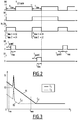
- the Figure 3 represents for two values of the bias current I 1 , I 2 , the noise graph B 1, respectively B2, affecting the measurement signal S 1, respectively S 2.
- the noise is dominated by the intrinsic noise of the gauge in 1 / f. Beyond a characteristic frequency, called the corner frequency fc1 , the noise is dominated by the thermal noise of the gauge and electronic acquisition means, which is a substantially constant noise as a function of frequency.
- the corner frequency moves to the low frequencies (fc2 ⁇ fc1).
- the signal-to-noise ratio remains at first substantially constant up to a critical value of the bias current, I c , and then decreases, in a second step, below this critical value.
- the first step 110 consists in defining the total consumption constraint of the device, that is to say not only the consumption for the polarization of the gauges 12 and 14, but also the consumption of the acquisition means 18.
- a bias current greater than the critical value I c is required . Since it is desired to minimize the bias current, it is necessary to be at the operating point corresponding to this critical value I c . It is shown that this critical value substantially corresponds to a polarization current such that the upper frequency fmax of the bandwidth of interest is equal to the corner frequency fc .
- step 120 the initial value of the bias current is determined, such that the corner frequency of the noise affecting the measurement signal corresponds to the maximum frequency of the bandwidth of interest.
- the adjustment means 25 makes it possible to adjust the value of the bias currents generated by the sources to this determined value.
- step 130 the value of the duty cycle of the chopping means is determined so as to reduce the power consumption. It is a question of minimizing the duty cycle to obtain the lowest power consumption, while keeping a certain margin with respect to the lowest possible consumption so as to take into account, depending on the chosen setup, the response time of the electronics (T guard on the Figure 2 ).
- the adjustment means 27 makes it possible to adjust the value of the duty ratio of the hash means to this determined value.
- step 140 the power consumption of the gauges is determined from the determined values of the bias current and the duty cycle. This consumption is subtracted from the total consumption defined in step 110 to obtain an electrical consumption that can be allocated to the acquisition means.
- This electrical consumption serves as a constraint for the development of the electronic amplification, filtering and digitizing chain for obtaining the measurement signal (step 150).
- the latter comprises a differential amplifier 65 connected to the power sources 22, 24 for effecting a feedback, so as to regulate the current supplied by the sources of power. current 22, 24.
- the differential amplifier 65 is for example an operational amplifier.
- the differential amplifier 65 comprises an input 65A receiving a mean voltage VAV corresponding to the average of the voltages taken at the input of the gages 12, 14 (or at the outputs of the current sources 22, 24), and an input 65 B receiving a control voltage VCM.
- the input 65A is non-inverting and the input 65B is inverting.
- the input 65A is inverting and the input 65B is non-inverting.
- the average voltage VAV is provided by an average module 66 comprising two inputs 66A, 66B each connected to the input of a respective gauge 12, 14 (or the output of a respective power source 22, 24) and a output 66C connected to input 65A input of the differential amplifier 65, the average module 66 providing at its output 66C a voltage which is the average of the voltages received at its inputs 66A, 66B.
- the output 65C of the differential amplifier 65 is connected to each current source 22, 24 so as to regulate the intensity of the current I bias1 , I bias2 , delivered by each of the current sources 22, 24 respectively.
- the current sources 22, 24 are, for example, transistors, in particular PMOS transistors, the output 65C of the differential amplifier 25 being connected to the gate of each current source 22, 24.
- the differential amplifier 65 dynamically regulates the current supplied by the current sources 22, 24 as a function of the difference between the average voltage VAV and the control voltage VCM. It compensates for common mode drifts, such as temperature variation. In case of temperature change, the voltage at the input of each gauge 12, 14 (or at the output of each current source 22, 24) varies but the voltage difference is kept constant.
- the silicon nanowire is biased current.
- a similar description could be made using a device in which the silicon nanowire is voltage-biased.
- the sensitive part of the device presented here comprises two gauges, but the invention operates regardless of the number of silicon nanowires used.
Description
L'invention a pour domaine celui des dispositifs résistifs du type comportant au moins une jauge de contrainte à nanofils de silicium, un moyen d'alimentation comportant au moins une source de courant propre à générer un courant de polarisation de la jauge, et des moyens d'acquisition propres à délivrer un signal de mesure à partir duquel la variation de la résistance électrique de la jauge peut être déterminée.The subject of the invention is that of resistive devices of the type comprising at least one strain gauge with silicon nanowires, a supply means comprising at least one current source capable of generating a bias current of the gauge, and means for acquiring a measurement signal from which the variation of the electrical resistance of the gauge can be determined.
De tels dispositifs sont connus, par exemple de l'article
Pour ce faire, la jauge doit être polarisée au sens où un courant de polarisation doit circuler à travers la nanofil de silicium.To do this, the gauge must be polarized in the sense that a bias current must flow through the silicon nanowire.
Le signal de mesure correspond alors à la variation de tension aux bornes de la résistance que constitue la jauge polarisée.The measurement signal then corresponds to the voltage variation across the resistor constituted by the polarized gauge.
Mais, la sensibilité du dispositif est limitée par le rapport signal de mesure sur bruit de fond (SNR pour « Signal to Noise Ratio » en anglais).But, the sensitivity of the device is limited by the ratio signal of measurement on background noise (SNR for "Signal to Noise Ratio" in English).
Une plus grande sensibilité, c'est-à-dire un SNR plus important, requiert une plus grande amplitude du signal de mesure qui est obtenue, toutes choses égales par ailleurs, par une augmentation du courant de polarisation de la jauge. Mais, l'augmentation du courant de polarisation conduit à une plus grande consommation électrique du dispositif.A greater sensitivity, ie a larger SNR, requires a greater amplitude of the measurement signal which is obtained, all things being equal, by an increase in the polarization current of the gauge. But, the increase in polarization current leads to greater power consumption of the device.
Ainsi, de manière générale, la sensibilité du dispositif et sa consommation électrique sont corrélées.Thus, in general, the sensitivity of the device and its power consumption are correlated.
De plus, de manière plus spécifique, dans certaines applications envisagées pour ces dispositifs, telles que capteurs inertiels corporels destinés à la détection du mouvement humain, l'information relative au mouvement est contenue dans la partie basse fréquence du signal de mesure délivré par le dispositif. Dans ces applications, la bande passante d'intérêt va, quasiment, du continu, jusqu'à quelques centaines de kilo Hertz.In addition, more specifically, in certain applications envisaged for these devices, such as body inertial sensors intended for the detection of human motion, the information relating to the movement is contained in the low frequency part of the measurement signal delivered by the device. . In these applications, the bandwidth of interest is almost continuous, up to a few hundred kilo Hertz.
Or, le bruit de fond d'un tel dispositif résulte de la superposition des bruits thermiques de la jauge et du moyen électronique d'acquisition, mais également d'un bruit intrinsèque de la jauge. Ce bruit intrinsèque de la jauge est en 1/f, c'est-à-dire proportionnel à l'inverse de la fréquence du signal mesuré. Plus la fréquence du signal de mesure est faible, plus le bruit est important.However, the background noise of such a device results from the superposition of the thermal noise of the gauge and the electronic means of acquisition, but also an intrinsic noise of the gauge. This intrinsic noise of the gauge is in 1 / f, that is to say proportional to the inverse of the frequency of the measured signal. The lower the frequency of the measurement signal, the greater the noise.
Pour obtenir une sensibilité acceptable à basse fréquence, il faut donc que l'amplitude du signal de mesure soit importante. Il faut par conséquent que le courant de polarisation des nanofils de silicium soit élevé. Ceci entraîne une consommation électrique supplémentaire du dispositif si on souhaite l'utiliser à basse fréquence.To obtain an acceptable sensitivity at low frequency, it is therefore necessary that the amplitude of the measurement signal is important. It is therefore necessary that the bias current of the silicon nanowires is high. This results in additional power consumption of the device if it is desired to use it at low frequency.
Or, la consommation électrique d'un tel dispositif résistif est un paramètre qui doit être minimisé. En effet, à côté des dispositifs résistifs, il existe une autre famille de dispositifs, les dispositifs capacitifs. Ceux-ci sont déjà largement utilisés en particulier parce qu'ils ne nécessitent pas de courant de polarisation pour fonctionner. Cela les rend fortement attractifs sur le plan de la consommation électrique totale du système qui les intègre.However, the power consumption of such a resistive device is a parameter that must be minimized. Indeed, next to the resistive devices, there is another family of devices, capacitive devices. These are already widely used especially because they do not require bias current to operate. This makes them highly attractive in terms of the total power consumption of the system that integrates them.
En revanche, la variation de la capacité avec la contrainte mécanique restant faible, ces dispositifs capacitifs intègrent nécessairement de fortes capacités qui sont, par nature, encombrantes. Ceci limite les possibilités d'intégration des systèmes utilisant de tels dispositifs capacitifs.On the other hand, since the variation of the capacitance with the mechanical stress remains low, these capacitive devices necessarily incorporate high capacities which are, by nature, bulky. This limits the possibilities of integration of systems using such capacitive devices.
Ainsi, pour les dispositifs résistifs à nanofil de silicium, qui sont des dispositifs compacts, se pose le problème de la réduction de leur consommation électrique sans pour autant dégrader leur SNR. La résolution de ce problème est déterminante pour que les dispositifs résistifs à nanofil de silicium soient utilisés plus largement dans l'industrie.Thus, for resistive silicon nanowire devices, which are compact devices, there is the problem of reducing their power consumption without degrading their SNR. The resolution of this problem is decisive for silicon nanowire resistive devices to be used more widely in the industry.
Il est par ailleurs connu, par exemple du document
L'invention a donc pour but de pallier, en tout ou partie, ce problème.The invention therefore aims to overcome, in whole or in part, this problem.
Pour cela l'invention a pour objet un dispositif résistif, un procédé d'optimisation et un procédé d'utilisation selon les revendications.For this purpose, the subject of the invention is a resistive device, an optimization method and a method of use according to the claims.
L'invention sera mieux comprise à la lecture de la description qui va suivre d'un mode de réalisation particulier, donnée uniquement à titre d'exemple et faite en se référant aux dessins annexés sur lesquels :
- la
Figure 1 est une représentation schématique du montage électrique d'un mode de réalisation préféré d'un dispositif résistif à nanofil de silicium ; - la
Figure 2 est un chronogramme représentant l'évolution temporelle de différents signaux de commande du montage de laFigure 1 ; - la
Figure 3 est un graphe représentant le bruit de fond affectant le dispositif de laFigure 1 pour deux valeurs différentes du courant de polarisation des jauges ; - la
Figure 4 est un graphe représentant l'évolution du rapport signal sur bruit (SNR) en fonction de la valeur du courant de polarisation ; - la
Figure 5 est un schéma blocs du procédé d'optimisation de la consommation électrique du dispositif de laFigure 1 ; et - la
Figure 6 est une représentation graphique partielle d'un mode de réalisation particulier du montage électrique de laFigure 1 .
- the
Figure 1 is a schematic representation of the electrical assembly of a preferred embodiment of a silicon nanowire resistive device; - the
Figure 2 is a chronogram representing the time evolution of various control signals of the assembly of theFigure 1 ; - the
Figure 3 is a graph representing the background noise affecting the device of theFigure 1 for two different values of the polarization current of the gages; - the
Figure 4 is a graph representing the evolution of the signal-to-noise ratio (SNR) as a function of the value of the bias current; - the
Figure 5 is a block diagram of the method of optimizing the power consumption of the device of theFigure 1 ; and - the
Figure 6 is a partial graphic representation of a particular embodiment of the electrical assembly of theFigure 1 .
Le dispositif résistif selon l'invention est un capteur inertiel à détection par nanofils de silicium. Il comporte, en tant qu'élément sensible, une masse sismique suspendue, de façon élastique, par deux nanofils de silicium s'étendant de part et d'autre de la masse, le long d'une direction X.The resistive device according to the invention is an inertial sensor with detection by silicon nanowires. It comprises, as sensitive element, a seismic mass suspended, elastically, by two silicon nanowires extending on either side of the mass, along a direction X.
Les nanofils de silicium, lorsqu'ils sont traversés par un courant de polarisation Ibias adapté, constituent des jauges de contrainte dont la variation de résistance électrique permet de déterminer l'accélération selon la direction X de la masse sismique.Silicon nanowires, when traversed by a bias bias current I adapted, constitute strain gauges whose variation of electrical resistance makes it possible to determine the acceleration in the X direction of the seismic mass.
La
Le dispositif 10 comporte deux jauges 12 et 14, un moyen d'alimentation 16 propre à générer un courant continu pour la polarisation des jauges 12 et 14, ainsi que des moyens d'acquisition 18 permettant de générer un signal de mesure à partir duquel il est possible de remonter à la variation de résistance de chacune des jauges et de déterminer l'accélération de la masse sismique.The device 10 comprises two
D'une manière générale, le montage de la
Le principal avantage d'un montage différentiel avec compensation du mode commun est de permettre la réduction de la dérive en température des jauges 12 et 14. Cette compensation du mode commun est préférable bien qu'elle ne soit pas indispensable à l'invention.The main advantage of a differential mounting with common mode compensation is to allow the reduction of the temperature drift of the
Ainsi, dans le montage de la
Le moyen d'alimentation 16 comporte deux sources de courant, respectivement 22 et 24, un moyen 25 de réglage de l'intensité du courant Ibias1, Ibias2, délivré par chacune des sources 22, 24, un étage de hachage 26 aux bornes d'entrée B et C duquel sont respectivement connectées les sources 22 et 24, un moyen 27 de réglage du rapport cyclique du moyen de hachage 26, et un étage de stabilisation par découpage 28 dont les bornes d'entrée G et H sont connectées aux bornes de sortie E et F du moyen de hachage 26, et dont les bornes de sortie I et J sont respectivement connectées aux bornes des jauges 12 et 14 qui ne sont pas connectées au noeud A.The power supply means 16 comprises two current sources, respectively 22 and 24, a
Le moyen de hachage 26 est équivalent à une paire d'interrupteurs commandés respectivement 32 et 34. Ces deux interrupteurs sont commandés par le même signal de commande de hachage M0 émis par le moyen 27. Lorsqu'il est fermé, l'interrupteur 32 permet l'application du courant I bias 1 généré par la source 22 sur la borne d'entrée G de l'étage 28.The hashing means 26 is equivalent to a pair of switches respectively controlled 32 and 34. These two switches are controlled by the same hash control signal M0 emitted by the
De manière similaire, lorsqu'il est fermé l'interrupteur 34 permet l'application du courant I bias 2 généré par la source 24 à la borne d'entrée H de l'étage 28.Similarly, when the
Le moyen de découpage 28 est équivalent à une paire de bascules commandées à deux états, respectivement 42 et 44.The cutting means 28 is equivalent to a pair of two-state controlled
Dans le premier état, la première bascule 42 permet de connecter la première borne d'entrée G à la première borne de sortie I tandis que la seconde bascule 44 permet simultanément de connecter la seconde borne d'entrée H à la seconde borne de sortie J du moyen 28.In the first state, the first flip-
Dans le second état, la première bascule 42 permet de connecter la première borne d'entrée G à la seconde borne de sortie J, tandis que la seconde bascule 44 permet simultanément de connecter la seconde borne d'entrée H à la première borne de sortie I du moyen 28.In the second state, the first flip-
L'état des bascules 42 et 44 est commandé par un même signal de contrôle de découpage M1.The state of the flip-
Les moyens d'acquisition 18 délivrent le signal de mesure.The acquisition means 18 deliver the measurement signal.
Les moyens 18 comportent un moyen de mesure du courant de polarisation comportant deux capteurs de courant respectivement 52 et 54. Chaque capteur est disposé en aval de l'une des sources de courant 22 et 24.The means 18 comprise means for measuring the bias current comprising two
Les moyens 18 comportent également un moyen de mesure de la tension aux bornes des jauges. Il comporte des amplificateurs respectivement des tensions prélevées au noeud B, amplificateur 56, et au noeud C, amplificateur 58 ; en aval des amplificateurs, un moyen de démodulation 60 représenté schématiquement ; en aval du moyen de démodulation 60, un filtre passe bas 62 ; et en aval du filtre 62, un moyen de numérisation, tel qu'un ADC 64, propre à numériser les signaux générés en sortie du filtre passe bas.The means 18 also comprise a means for measuring the voltage across the gauges. It comprises amplifiers respectively voltages taken at node B,
La fonction du moyen de démodulation 60 est la démodulation des signaux de tension amplifiés résultant de la modulation de l'application des courants de polarisation aux jauges 12 et 14 par le moyen de découpage 28. Le moyen 60 est commandé par deux signaux de commande de démodulation respectivement D0 et D1.The function of the demodulation means 60 is the demodulation of the amplified voltage signals resulting from the modulation of the application of the bias currents to the
Les signaux de commande pour le fonctionnement du dispositif de la
Le signal de commande de hachage M0 est un signal créneau entre les valeurs 0 et 1. Il prend la valeur 0 sur une première période Tbias d'un demi cycle de fonctionnement, et la valeur 1 sur le reste de ce demi cycle de fonctionnement.The hash control signal M0 is a slot signal between the
Le rapport de la durée Tbias sur la durée d'un demi cycle T1/2 cycle correspond au rapport cyclique.The ratio of the duration T bias on the duration of a half cycle T 1/2 cycle corresponds to the duty cycle.
Lorsque le signal de commande de hachage M0 a la valeur 0, les interrupteurs 32 et 34 sont fermés de sorte que le courant I bias 1 généré par la source 22 est appliqué à la première borne d'entrée G de l'étage 28, tandis que le courant I bias 2 généré par la source 24 est appliqué à la seconde borne d'entrée H de l'étage 28.When the hash control signal M0 has the
Lorsque le signal de commande M0 prend la valeur 1, les interrupteurs 32 et 34 sont ouverts.When the control signal M0 takes the
Le signal de commande de découpage M1 est un signal créneau entre les valeurs 0 et 1. Il prend la valeur 0 sur le premier demi-cycle et la valeur 1 sur le second demi-cycle suivant de fonctionnement du dispositif 10.The chopping control signal M1 is a slot signal between the
Lorsque le signal de commande M1 prend la valeur 0, les première et seconde bascules 42 et 44 sont dans le premier état. Le courant I bias 1 circule alors dans la jauge 12 et le courant I bias 2 dans la jauge 14.When the control signal M1 has the
En revanche, lorsque le signal de commande M1 prend la valeur 1, les première et seconde bascules sont dans le second état. Le courant I bias 2 circule dans la jauge 12 et le courant I bias 1, dans la jauge 14.On the other hand, when the control signal M1 takes the
Le troisième chronogramme de la
- pendant une première période Tbias du premier demi-cycle, le courant I bias 1 traverse la première jauge 12 tandis que le courant I2 traverse la seconde jauge 14 ;
- pendant le reste de ce premier demi-cycle aucun courant ne circule à travers les jauges ;
- durant une première période Tbias du second demi-cycle, le courant I bias 1circule dans la seconde jauge 14, tandis que le second courant I bias 2 circule à travers la première jauge 12 ; et,
- durant le reste de ce second demi-cycle aucun courant ne circule dans les jauges.
- during a first period T bias of the first half-cycle, the current I bias 1 through the
first gauge 12 while the current I2 through thesecond gauge 14; - during the remainder of this first half cycle no current flows through the gauges;
- during a first period T bias of the second half cycle, the current I bias 1 flows in the
second gauge 14, while the second current I bias 2 flows through thefirst gauge 12; and, - during the remainder of this second half-cycle no current flows in the gauges.
Sur la
De manière similaire, le signal D1 est essentiellement nul, sauf pendant un intervalle de temps Tmes inclus dans la première période du second demi-cycle.Similarly, the signal D1 is essentially zero, except during a time interval T mes included in the first period of the second half-cycle.
Ainsi, lors de l'utilisation du dispositif 10, les jauges 12 et 14 sont polarisées par un courant électrique durant une fraction du cycle d'utilisation du dispositif. Dit autrement, les jauges sont polarisées alternativement par les courants I bias 1 et I bias 2 pendant la durée de la mesure, cette mesure n'étant effectuée que pendant une période de temps Tbias réduite par rapport au cycle d'utilisation (période d'échantillonnage) du dispositif. Pendant le reste du temps, aucun courant ne circule dans les jauges qui ont donc une consommation électrique nulle.Thus, during the use of the device 10, the
Cette capacité de n'utiliser les jauges que sur une fraction du cycle est due au temps de réponse des nanofils de silicium qui est extrêmement bas par rapport au temps de réponse plus élevé des moyens électroniques d'acquisition 18.This ability to use the gages only for a fraction of the cycle is due to the silicon nanowires response time which is extremely low compared to the higher response time of the electronic acquisition means 18.
Ainsi, le moyen de hachage permet de réduire la consommation électrique du dispositif en ne polarisant que temporairement les jauges.Thus, the hashing means reduces the power consumption of the device by only polarizing the gauges temporarily.
Mais, il a été découvert de manière surprenante, que le fait d'appliquer un courant de polarisation de manière alternative à travers une jauge du type nanofil de silicium atténue fortement le bruit intrinsèque de cette jauge. Des observations expérimentales ont été faites pour montrer que pour les fréquences faibles, il n'y a pas de dégradation du rapport signal sur bruit lorsque l'on réduit le rapport cyclique de 75 à 25%. Le fait de réduire le rapport cyclique conduit à une diminution de la puissance moyenne du courant de polarisation et, par conséquent, à une diminution de la puissance moyenne du signal de mesure. Mais pourtant, le SNR reste sensiblement constant. On déduit donc que le hachage réduit la puissance du bruit intrinsèque de la jauge.However, it has surprisingly been found that applying an alternating polarization current through a silicon nanowire type gauge strongly attenuates the intrinsic noise of this gage. Experimental observations have been made to show that for low frequencies, there is no degradation of the signal-to-noise ratio when the duty cycle is reduced from 75 to 25%. Reducing the duty cycle leads to a decrease in the average power of the bias current and, therefore, to a decrease in the average power of the measurement signal. But nevertheless, the SNR remains substantially constant. It is therefore deduced that the hash reduces the power of the intrinsic noise of the gauge.
Pour profiter pleinement de cet effet d'atténuation du bruit intrinsèque en 1/f de la jauge, le courant de polarisation Ibias est réglé au moyen du moyen de réglage 25 de la manière suivante.To take full advantage of this intrinsic noise attenuation effect in 1 / f of the gauge, the polarization current I bias is adjusted by means of the adjusting means 25 in the following manner.
La
Dans une première partie du graphe, partie correspondant aux fréquences faibles, le bruit est dominé par le bruit intrinsèque de la jauge en 1/f. Au-delà d'une fréquence caractéristique, appelée fréquence de coin fc1, le bruit est dominé par le bruit thermique de la jauge et des moyens électroniques d'acquisition, qui est un bruit sensiblement constant en fonction de la fréquence.In a first part of the graph, part corresponding to low frequencies, the noise is dominated by the intrinsic noise of the gauge in 1 / f. Beyond a characteristic frequency, called the corner frequency fc1 , the noise is dominated by the thermal noise of the gauge and electronic acquisition means, which is a substantially constant noise as a function of frequency.
Lorsque le courant de polarisation est diminué, la fréquence de coin se déplace vers les fréquences faibles (fc2<fc1).When the bias current is decreased, the corner frequency moves to the low frequencies (fc2 <fc1).
On a représenté sur la
On constate que, lorsque le courant de polarisation diminue, le rapport signal sur bruit reste dans un premier temps sensiblement constant jusqu'à une valeur critique du courant de polarisation, Ic, puis diminue, dans un second temps, en-deçà de cette valeur critique.It can be seen that, when the bias current decreases, the signal-to-noise ratio remains at first substantially constant up to a critical value of the bias current, I c , and then decreases, in a second step, below this critical value.
Ceci est dû au fait que, pour les courants de polarisation supérieurs à cette valeur critique Ic, le bruit de fond est dominé par le bruit intrinsèque en 1/f qui est dans un rapport constant avec l'amplitude du signal de mesure comme indiqué ci-dessus.This is because, for polarization currents above this critical value I c , the background noise is dominated by the intrinsic 1 / f noise which is in a constant relationship with the amplitude of the measurement signal as indicated. above.
En revanche, pour les courants de polarisation inférieurs à cette valeur critique Ic, le bruit de fond est dominé par le bruit thermique. Le bruit thermique étant constant, lorsque le courant de polarisation diminue, l'amplitude du signal de mesure diminue et le SNR ne peut que diminuer.On the other hand, for polarization currents lower than this critical value I c , the background noise is dominated by thermal noise. Since the thermal noise is constant, when the bias current decreases, the amplitude of the measurement signal decreases and the SNR can only decrease.
On en déduit le procédé suivant d'optimisation du courant de polarisation des dispositifs.From this is deduced the following method of optimizing the polarization current of the devices.
Ce procédé est représenté à la
Pour bénéficier de l'atténuation du bruit intrinsèque par le hachage du courant de polarisation, il faut un courant de polarisation supérieur à la valeur critique Ic. Puisque l'on souhaite minimiser le courant de polarisation, il faut donc se placer au point de fonctionnement correspondant à cette valeur critique Ic. On montre que cette valeur critique correspond sensiblement à un courant de polarisation tel que la fréquence supérieure fmax de la bande passante d'intérêt soit égale à la fréquence de coin fc.To benefit from the intrinsic noise attenuation by the hashing of the bias current, a bias current greater than the critical value I c is required . Since it is desired to minimize the bias current, it is necessary to be at the operating point corresponding to this critical value I c . It is shown that this critical value substantially corresponds to a polarization current such that the upper frequency fmax of the bandwidth of interest is equal to the corner frequency fc .
On détermine ainsi, à l'étape 120, la valeur initiale du courant de polarisation, telle que la fréquence de coin du bruit affectant le signal de mesure corresponde à la fréquence maximale de la bande passante d'intérêt. Lors de l'utilisation du dispositif, le moyen de réglage 25 permet d'ajuster la valeur des courants de polarisation générés par les sources, à cette valeur déterminée.Thus, in
A l'étape 130, on détermine la valeur du rapport cyclique du moyen de hachage de manière à réduire la consommation électrique. Il s'agit de minimiser le rapport cyclique pour obtenir la consommation électrique la plus faible, tout en conservant une certaine marge par rapport à la consommation la plus faible possible de manière à tenir compte, en fonction du montage choisi, du temps de réponse de l'électronique (Tguard sur la
Enfin, à l'étape 140, on détermine la consommation électrique des jauges à partir des valeurs déterminées du courant de polarisation et du rapport cyclique. Cette consommation est soustraite de la consommation totale définie à l'étape 110 pour obtenir une consommation électrique que l'on peut affecter aux moyens d'acquisition.Finally, in
Cette consommation électrique sert alors de contrainte pour l'élaboration de la chaîne électronique d'amplification, de filtrage et de numérisation permettant d'obtenir le signal de mesure (étape 150).This electrical consumption then serves as a constraint for the development of the electronic amplification, filtering and digitizing chain for obtaining the measurement signal (step 150).
Au cours de l'utilisation du dispositif, le point de fonctionnement optimal est, par exemple, le suivant :
- Ibias1 = Ibias2 = 1/2.10-4 A
- R = 2,5 kΩ et ΔR/R=+/- 3,6.10-2
- I bias1 = I bias2 = 1 / 2.10 -4 A
- R = 2.5 kΩ and ΔR / R = +/- 3.6.10 -2
Où ΔR/R est la sensibilité du nanofil de silicium.
- gamme des fréquences fmin =0,1 Hz ; fmax = 1000 Hz
- SNR = 74 dB
- I total = 2 x Ibias + Iacq = 120.10-6A
- frequency range f min = 0.1 Hz; f max = 1000 Hz
- SNR = 74 dB
- I total = 2 x I bias + I acq = 120.10 -6 A
Où Iacq est l'intensité du courant dans les moyens d'acquisition.
- la puissance totale du dispositif : P=15 µW. Acq where I is the intensity of the current in the acquisition means.
the total power of the device: P = 15 μW.
De nombreuses variantes du dispositif sont à envisager.Many variants of the device are to be considered.
Dans le mode de réalisation illustré sur la
L'amplificateur différentiel 65 est par exemple un amplificateur opérationnel.The
L'amplificateur différentiel 65 comprend une entrée 65A recevant une tension moyenne VAV correspondant à la moyenne des tensions prises en entrée des jauges 12, 14 (ou en sorties des sources de courant 22, 24), et une entrée 65B recevant une tension de commande VCM. Tel que représentées sur la
La tension moyenne VAV est fournie par un module de moyenne 66 comprenant deux entrée 66A, 66B chacune reliée à l'entrée d'une jauge 12, 14 respective (ou à la sortie d'une source de courant 22, 24 respective) et une sortie 66C reliée à l'entrée 65A entrée de l'amplificateur différentiel 65, le module de moyenne 66 fournissant à sa sortie 66C une tension qui est la moyenne des tensions reçues à ses entrées 66A, 66B.The average voltage VAV is provided by an
La sortie 65C de l'amplificateur différentiel 65 est reliée à chaque source de courant 22, 24 de manière à réguler l'intensité du courant Ibias1, Ibias2, délivré par chacune des sources de courant 22, 24 respectivement.The
Les sources de courant 22, 24 sont par exemple des transistors, notamment transistors PMOS, la sortie 65C de l'amplificateur différentiel 25 étant reliée à la grille de chaque source de courant 22, 24.The
L'amplificateur différentiel 65 régule dynamiquement le courant fourni par les sources de courant 22, 24 en fonction de la différence entre la tension moyenne VAV et la tension de commande VCM. Il compense ainsi les dérives de mode commun, telle que la variation de température. En cas de changement de température, la tension à l'entrée de chaque jauge 12, 14 (ou à la sortie de chaque source de courant 22, 24) varie mais la différence de tension est maintenue constante.The
Le courant de polarisation Ibias est réglé initialement en jouant sur VCM et/ou VREF de telle manière que Ibias= (VCM - VREF)/RJ où RJ représente la résistance ohmique des jauges 12, 14.The bias current I bias is initially set by acting on VCM and / or VREF such that I bias = (VCM - VREF) / R J where R J represents the ohmic resistance of the
Dans le mode de réalisation venant d'être décrit en détail, la nanofil de silicium est polarisé en courant. Une description similaire pourrait être faite en utilisant un dispositif dans lequel le nanofil de silicium est polarisé en tension.In the embodiment just described in detail, the silicon nanowire is biased current. A similar description could be made using a device in which the silicon nanowire is voltage-biased.
Bien évidemment, la partie sensible du dispositif présenté ici comporte deux jauges, mais l'invention fonctionne quel que soit le nombre de nanofils de silicium utilisé.Obviously, the sensitive part of the device presented here comprises two gauges, but the invention operates regardless of the number of silicon nanowires used.
Claims (12)
- A method for optimising the power consumption of a resistive device (10) of the type comprising :- at least one silicon nanowire strain gauge (12, 14),- a power supply means (16) comprising at least one current source (22, 24) able to generate a current (Ibias) for biasing the gauge, and- an acquisition means (18) able to deliver a measurement signal which can be used to determine the variation of an electrical resistance of the gauge,the power supply means comprises a chopping means (26), capable of allowing the biasing current generated by the or each current source to flow through the or each gauge only during a fraction of an operating cycle of the device, characterised in that said method comprises the following steps of:- defining an acceptable total consumption for the device (10);- calculating the value of a biasing current in a manner such that the upper frequency (fmax) of the bandwidth of interest for the measurement signal corresponds to a corner frequency (fc) of a background noise affecting the device;- adjusting the chopping means in a manner such that the power supply duty cycle ratio of the gauges leads to a predetermined signal to noise ratio for the device;- calculating the power consumption of said at least one gauge (12, 14) taking into account the calculated value of the biasing current and the value of the duty cycle determined;- evaluating a difference between the total acceptable consumption and the consumption of the said at least one strain gauge and assigning this difference as a constraint for the development of the electronic acquisition means (18).
- A method of use of a resistive device (10) optimised according to claim 1, the resistive device comprising:- at least one silicon nanowire strain gauge (12, 14),- a power supply means (16) comprising at least one current source (22, 24) able to generate a current (Ibias) for biasing the gauge, and- an acquisition means (18) able to deliver a measurement signal which can be used to determine the variation of an electrical resistance of the gauge,the power supply means comprises a chopping means (26), capable of allowing the biasing current generated by the or each current source to flow through the or each gauge only during a fraction of an operating cycle of the device, characterised in that said method includes a step of calculating the value of the biasing current in a manner such that an upper frequency (fmax) of a bandwidth of interest for the measurement signal delivered by the resistive device corresponds to a corner frequency (fc) of a background noise affecting the device, and a step of adjusting the said power supply means in a manner such that the biasing current in the gauge is equal to the calculated biasing current.
- A method according to claim 2, characterised in that it comprises a step of adjusting the said chopping means in a manner such that the power supply duty cycle ratio of the gauge corresponds to a predetermined signal to noise ratio.
- A method according to any one of preceding claims, characterised in that the said chopping means of said device comprises a means for adjusting the duty cycle ratio, capable of adjusting said fraction of an operating cycle of the device to a value less than 75%, preferably less than 50%, in particular equal to 25%.
- A method according to any one of the preceding claims, characterised in that the lower frequency of the bandwidth of interest for the measurement signal delivered by the device substantially corresponds to a zero frequency (fmin).
- A method according to any one of the preceding claims, characterised in that the acquisition means comprise a stage of amplification (58, 56), a means for filtering (62) and a means for digitising (64).
- A method according to any one of the preceding claims, characterised in that it comprises two silicon nanowire strain gauges incorporated in an electrical circuit of the differential type.
- A method according to claim 7, characterised in that the power supply means comprises two current sources (22, 24), each capable of generating a current for biasing one of the gauges.
- A method according to claim 8, characterised in that the power supply means further comprises a means for stabilisation by switching (28), and in that the acquisition means (18) comprises a demodulation means (60) positioned between the stage of amplification and the filtering means, the control signals (D0, D1) of the demodulation stage being correlated with the control signals (M0 , M1) of the means for stabilisation by switching and / or of the chopping means.
- A method according to any one of claims 7 to 9, characterised in that the said electrical circuit arrangement of the two gauges allows a common mode compensation.
- A method according to any one of claims 7 to 10, characterised in that it comprises a differential amplifier (65) having two inputs and one output, one input receiving the average voltage of the inputs of the gauges (12, 14) or the outputs of the current sources (22, 24), the other input receiving a control voltage, and the output being connected to each current source (22, 24) in a manner so as to regulate the intensity of the current delivered by each of the current sources (22, 24).
- A method according to any one of the preceding claims, characterised in that it is an inertial sensor.
Applications Claiming Priority (2)
| Application Number | Priority Date | Filing Date | Title |
|---|---|---|---|
| FR1155884A FR2977318B1 (en) | 2011-06-30 | 2011-06-30 | SILICON NANOWILE STRAIN GAUGE RESISITIVE DEVICE AND METHOD OF OPTIMIZING THE ELECTRICAL CONSUMPTION OF SUCH A DEVICE |
| PCT/EP2012/062774 WO2013001081A1 (en) | 2011-06-30 | 2012-06-29 | Resistive device comprising a silcon-nanowire-comprising strain gauge and method for optimizing the electrical consumption of such a device |
Publications (2)
| Publication Number | Publication Date |
|---|---|
| EP2726832A1 EP2726832A1 (en) | 2014-05-07 |
| EP2726832B1 true EP2726832B1 (en) | 2016-11-02 |
Family
ID=46420201
Family Applications (1)
| Application Number | Title | Priority Date | Filing Date |
|---|---|---|---|
| EP12730972.2A Active EP2726832B1 (en) | 2011-06-30 | 2012-06-29 | Resistive device comprising a silcon-nanowire-comprising strain gauge and method for optimizing the electrical consumption of such a device |
Country Status (4)
| Country | Link |
|---|---|
| US (1) | US9134191B2 (en) |
| EP (1) | EP2726832B1 (en) |
| FR (1) | FR2977318B1 (en) |
| WO (1) | WO2013001081A1 (en) |
Families Citing this family (7)
| Publication number | Priority date | Publication date | Assignee | Title |
|---|---|---|---|---|
| US10317297B2 (en) * | 2013-12-11 | 2019-06-11 | Melexis Technologies Nv | Semiconductor pressure sensor |
| EP3146534A4 (en) | 2014-05-19 | 2018-04-18 | The Regents of The University of California | Flexible sensor apparatus |
| US11207002B2 (en) * | 2014-05-19 | 2021-12-28 | The Regents Of The University Of California | Fetal health monitor |
| US10780688B2 (en) | 2016-02-17 | 2020-09-22 | The Regents Of The University Of California | Highly wrinkled metal thin films using lift-off layers |
| US10898084B2 (en) | 2016-03-31 | 2021-01-26 | The Regents Of The University Of California | Vital signs monitor |
| US11839453B2 (en) | 2016-03-31 | 2023-12-12 | The Regents Of The University Of California | Soft capacitive pressure sensors |
| US10788375B2 (en) | 2017-12-07 | 2020-09-29 | Tower Semiconductor Ltd. | Apparatus, system and method of a temperature sensor |
Family Cites Families (5)
| Publication number | Priority date | Publication date | Assignee | Title |
|---|---|---|---|---|
| US6970742B2 (en) * | 2000-01-11 | 2005-11-29 | Savacor, Inc. | Method for detecting, diagnosing, and treating cardiovascular disease |
| US6433524B1 (en) * | 2001-03-15 | 2002-08-13 | Rosemount Aerospace Inc. | Resistive bridge interface circuit |
| US7991467B2 (en) * | 2005-04-26 | 2011-08-02 | Medtronic, Inc. | Remotely enabled pacemaker and implantable subcutaneous cardioverter/defibrillator system |
| US20070074584A1 (en) * | 2005-10-03 | 2007-04-05 | Joseph Talarico | Gentle touch surgical instrument and method of using same |
| FR2917731B1 (en) * | 2007-06-25 | 2009-10-23 | Commissariat Energie Atomique | DEVICE RESONANT TO PIEZORESISTIVE DETECTION REALIZED IN SURFACE TECHNOLOGIES |
-
2011
- 2011-06-30 FR FR1155884A patent/FR2977318B1/en active Active
-
2012
- 2012-06-29 EP EP12730972.2A patent/EP2726832B1/en active Active
- 2012-06-29 WO PCT/EP2012/062774 patent/WO2013001081A1/en active Application Filing
- 2012-06-29 US US14/129,804 patent/US9134191B2/en active Active
Also Published As
| Publication number | Publication date |
|---|---|
| US9134191B2 (en) | 2015-09-15 |
| US20140290376A1 (en) | 2014-10-02 |
| FR2977318A1 (en) | 2013-01-04 |
| EP2726832A1 (en) | 2014-05-07 |
| FR2977318B1 (en) | 2013-08-09 |
| WO2013001081A1 (en) | 2013-01-03 |
Similar Documents
| Publication | Publication Date | Title |
|---|---|---|
| EP2726832B1 (en) | Resistive device comprising a silcon-nanowire-comprising strain gauge and method for optimizing the electrical consumption of such a device | |
| EP0285478B1 (en) | Circuit for converting analogous signals into digital signals | |
| EP2304872B1 (en) | Circuit for amplifying a signal representing a variation in resistance of a variable resistance and corresponding capacitor | |
| EP2933224B1 (en) | Measurement circuit | |
| EP0333572A1 (en) | Formatting and utilisation device for induced waves generated by a DC motor, especially for position control | |
| EP0510061B1 (en) | Device for measuring the variations in the capacitance of a capacitor, particularly a detector | |
| EP3244169B1 (en) | Resonant measurement system with improved resolution | |
| FR2625322A1 (en) | CURRENT SENSOR WITH MAGNETORESISTIVE ELEMENT | |
| FR2632793A1 (en) | IMPROVED BUTTON EXPLOITING THE PROPERTIES OF A LIQUID CRYSTAL | |
| EP1762854B1 (en) | Measuring device for very short current impulses | |
| FR2700083A1 (en) | Stable distortion amplifier for audio signals. | |
| EP0816795B1 (en) | Instrument for measuring lengths or angles | |
| EP2618163A1 (en) | Method for measuring a physical parameter and electronic circuit to interface with a capacitive sensor for implementing same | |
| EP2567245B1 (en) | Device for measuring the local electrical resistance of a surface | |
| EP2232273A2 (en) | Method of correcting the gain of a capacitive unit and device for implementing same | |
| EP3149504B1 (en) | Magnetometric sensor | |
| EP0973153A1 (en) | Magnetic information read device | |
| WO2020156973A1 (en) | Tracer gas leak detection system and corresponding use | |
| EP2889595B1 (en) | Method for managing a supply of current or voltage of a resistive temperature sensor arranged inside a cryogenic enclosure | |
| FR2458946A1 (en) | INTEGRATING CELL FOR FORMING A FILTER, THIS FILTER AND ITS APPLICATION TO THE DETECTION OF VIBRATION LEVELS | |
| EP0857964A1 (en) | Method and apparatus for determining gas concentration | |
| EP1601986A2 (en) | System for measuring a low-frequency magnetic field and system for modulating a magnetic field used in said measuring system | |
| FR2797959A1 (en) | Gain adjuster for magnetic field sensor, has gain compensation for signal strength variation reduces effect of mechanical tolerances | |
| FR2817046A1 (en) | Low noise current amplifier with programmable gain and polarization for use in electrical measurement of semiconductor circuits, such as transistors, with the circuit being low noise and having a protection circuit for the input | |
| FR2951887A1 (en) | SYSTEM AND METHOD FOR CONTROLLING A DIGITAL SENSOR |
Legal Events
| Date | Code | Title | Description |
|---|---|---|---|
| PUAI | Public reference made under article 153(3) epc to a published international application that has entered the european phase |
Free format text: ORIGINAL CODE: 0009012 |
|
| 17P | Request for examination filed |
Effective date: 20131230 |
|
| AK | Designated contracting states |
Kind code of ref document: A1 Designated state(s): AL AT BE BG CH CY CZ DE DK EE ES FI FR GB GR HR HU IE IS IT LI LT LU LV MC MK MT NL NO PL PT RO RS SE SI SK SM TR |
|
| DAX | Request for extension of the european patent (deleted) | ||
| REG | Reference to a national code |
Ref country code: DE Ref legal event code: R079 Ref document number: 602012024839 Country of ref document: DE Free format text: PREVIOUS MAIN CLASS: G01L0001220000 Ipc: B82Y0010000000 |
|
| GRAP | Despatch of communication of intention to grant a patent |
Free format text: ORIGINAL CODE: EPIDOSNIGR1 |
|
| RIC1 | Information provided on ipc code assigned before grant |
Ipc: H01L 29/8605 20060101ALI20160422BHEP Ipc: B82Y 10/00 20110101AFI20160422BHEP Ipc: G01L 1/22 20060101ALI20160422BHEP Ipc: H01L 29/06 20060101ALI20160422BHEP Ipc: G01P 15/12 20060101ALI20160422BHEP Ipc: H01L 29/16 20060101ALI20160422BHEP |
|
| INTG | Intention to grant announced |
Effective date: 20160527 |
|
| GRAS | Grant fee paid |
Free format text: ORIGINAL CODE: EPIDOSNIGR3 |
|
| GRAA | (expected) grant |
Free format text: ORIGINAL CODE: 0009210 |
|
| AK | Designated contracting states |
Kind code of ref document: B1 Designated state(s): AL AT BE BG CH CY CZ DE DK EE ES FI FR GB GR HR HU IE IS IT LI LT LU LV MC MK MT NL NO PL PT RO RS SE SI SK SM TR |
|
| REG | Reference to a national code |
Ref country code: GB Ref legal event code: FG4D Free format text: NOT ENGLISH |
|
| REG | Reference to a national code |
Ref country code: AT Ref legal event code: REF Ref document number: 841640 Country of ref document: AT Kind code of ref document: T Effective date: 20161115 Ref country code: CH Ref legal event code: EP |
|
| REG | Reference to a national code |
Ref country code: IE Ref legal event code: FG4D Free format text: LANGUAGE OF EP DOCUMENT: FRENCH |
|
| REG | Reference to a national code |
Ref country code: DE Ref legal event code: R096 Ref document number: 602012024839 Country of ref document: DE |
|
| PG25 | Lapsed in a contracting state [announced via postgrant information from national office to epo] |
Ref country code: LV Free format text: LAPSE BECAUSE OF FAILURE TO SUBMIT A TRANSLATION OF THE DESCRIPTION OR TO PAY THE FEE WITHIN THE PRESCRIBED TIME-LIMIT Effective date: 20161102 |
|
| REG | Reference to a national code |
Ref country code: NL Ref legal event code: MP Effective date: 20161102 |
|
| REG | Reference to a national code |
Ref country code: LT Ref legal event code: MG4D |
|
| REG | Reference to a national code |
Ref country code: AT Ref legal event code: MK05 Ref document number: 841640 Country of ref document: AT Kind code of ref document: T Effective date: 20161102 |
|
| PG25 | Lapsed in a contracting state [announced via postgrant information from national office to epo] |
Ref country code: NL Free format text: LAPSE BECAUSE OF FAILURE TO SUBMIT A TRANSLATION OF THE DESCRIPTION OR TO PAY THE FEE WITHIN THE PRESCRIBED TIME-LIMIT Effective date: 20161102 Ref country code: SE Free format text: LAPSE BECAUSE OF FAILURE TO SUBMIT A TRANSLATION OF THE DESCRIPTION OR TO PAY THE FEE WITHIN THE PRESCRIBED TIME-LIMIT Effective date: 20161102 Ref country code: NO Free format text: LAPSE BECAUSE OF FAILURE TO SUBMIT A TRANSLATION OF THE DESCRIPTION OR TO PAY THE FEE WITHIN THE PRESCRIBED TIME-LIMIT Effective date: 20170202 Ref country code: GR Free format text: LAPSE BECAUSE OF FAILURE TO SUBMIT A TRANSLATION OF THE DESCRIPTION OR TO PAY THE FEE WITHIN THE PRESCRIBED TIME-LIMIT Effective date: 20170203 Ref country code: LT Free format text: LAPSE BECAUSE OF FAILURE TO SUBMIT A TRANSLATION OF THE DESCRIPTION OR TO PAY THE FEE WITHIN THE PRESCRIBED TIME-LIMIT Effective date: 20161102 |
|
| REG | Reference to a national code |
Ref country code: FR Ref legal event code: PLFP Year of fee payment: 6 |
|
| PG25 | Lapsed in a contracting state [announced via postgrant information from national office to epo] |
Ref country code: AT Free format text: LAPSE BECAUSE OF FAILURE TO SUBMIT A TRANSLATION OF THE DESCRIPTION OR TO PAY THE FEE WITHIN THE PRESCRIBED TIME-LIMIT Effective date: 20161102 Ref country code: HR Free format text: LAPSE BECAUSE OF FAILURE TO SUBMIT A TRANSLATION OF THE DESCRIPTION OR TO PAY THE FEE WITHIN THE PRESCRIBED TIME-LIMIT Effective date: 20161102 Ref country code: RS Free format text: LAPSE BECAUSE OF FAILURE TO SUBMIT A TRANSLATION OF THE DESCRIPTION OR TO PAY THE FEE WITHIN THE PRESCRIBED TIME-LIMIT Effective date: 20161102 Ref country code: PL Free format text: LAPSE BECAUSE OF FAILURE TO SUBMIT A TRANSLATION OF THE DESCRIPTION OR TO PAY THE FEE WITHIN THE PRESCRIBED TIME-LIMIT Effective date: 20161102 Ref country code: ES Free format text: LAPSE BECAUSE OF FAILURE TO SUBMIT A TRANSLATION OF THE DESCRIPTION OR TO PAY THE FEE WITHIN THE PRESCRIBED TIME-LIMIT Effective date: 20161102 Ref country code: FI Free format text: LAPSE BECAUSE OF FAILURE TO SUBMIT A TRANSLATION OF THE DESCRIPTION OR TO PAY THE FEE WITHIN THE PRESCRIBED TIME-LIMIT Effective date: 20161102 Ref country code: PT Free format text: LAPSE BECAUSE OF FAILURE TO SUBMIT A TRANSLATION OF THE DESCRIPTION OR TO PAY THE FEE WITHIN THE PRESCRIBED TIME-LIMIT Effective date: 20170302 Ref country code: IS Free format text: LAPSE BECAUSE OF FAILURE TO SUBMIT A TRANSLATION OF THE DESCRIPTION OR TO PAY THE FEE WITHIN THE PRESCRIBED TIME-LIMIT Effective date: 20170302 |
|
| PG25 | Lapsed in a contracting state [announced via postgrant information from national office to epo] |
Ref country code: CZ Free format text: LAPSE BECAUSE OF FAILURE TO SUBMIT A TRANSLATION OF THE DESCRIPTION OR TO PAY THE FEE WITHIN THE PRESCRIBED TIME-LIMIT Effective date: 20161102 Ref country code: RO Free format text: LAPSE BECAUSE OF FAILURE TO SUBMIT A TRANSLATION OF THE DESCRIPTION OR TO PAY THE FEE WITHIN THE PRESCRIBED TIME-LIMIT Effective date: 20161102 Ref country code: EE Free format text: LAPSE BECAUSE OF FAILURE TO SUBMIT A TRANSLATION OF THE DESCRIPTION OR TO PAY THE FEE WITHIN THE PRESCRIBED TIME-LIMIT Effective date: 20161102 Ref country code: DK Free format text: LAPSE BECAUSE OF FAILURE TO SUBMIT A TRANSLATION OF THE DESCRIPTION OR TO PAY THE FEE WITHIN THE PRESCRIBED TIME-LIMIT Effective date: 20161102 Ref country code: SK Free format text: LAPSE BECAUSE OF FAILURE TO SUBMIT A TRANSLATION OF THE DESCRIPTION OR TO PAY THE FEE WITHIN THE PRESCRIBED TIME-LIMIT Effective date: 20161102 |
|
| REG | Reference to a national code |
Ref country code: DE Ref legal event code: R097 Ref document number: 602012024839 Country of ref document: DE |
|
| PG25 | Lapsed in a contracting state [announced via postgrant information from national office to epo] |
Ref country code: BG Free format text: LAPSE BECAUSE OF FAILURE TO SUBMIT A TRANSLATION OF THE DESCRIPTION OR TO PAY THE FEE WITHIN THE PRESCRIBED TIME-LIMIT Effective date: 20170202 Ref country code: SM Free format text: LAPSE BECAUSE OF FAILURE TO SUBMIT A TRANSLATION OF THE DESCRIPTION OR TO PAY THE FEE WITHIN THE PRESCRIBED TIME-LIMIT Effective date: 20161102 Ref country code: IT Free format text: LAPSE BECAUSE OF FAILURE TO SUBMIT A TRANSLATION OF THE DESCRIPTION OR TO PAY THE FEE WITHIN THE PRESCRIBED TIME-LIMIT Effective date: 20161102 |
|
| PLBE | No opposition filed within time limit |
Free format text: ORIGINAL CODE: 0009261 |
|
| STAA | Information on the status of an ep patent application or granted ep patent |
Free format text: STATUS: NO OPPOSITION FILED WITHIN TIME LIMIT |
|
| 26N | No opposition filed |
Effective date: 20170803 |
|
| PG25 | Lapsed in a contracting state [announced via postgrant information from national office to epo] |
Ref country code: SI Free format text: LAPSE BECAUSE OF FAILURE TO SUBMIT A TRANSLATION OF THE DESCRIPTION OR TO PAY THE FEE WITHIN THE PRESCRIBED TIME-LIMIT Effective date: 20161102 |
|
| PG25 | Lapsed in a contracting state [announced via postgrant information from national office to epo] |
Ref country code: MC Free format text: LAPSE BECAUSE OF FAILURE TO SUBMIT A TRANSLATION OF THE DESCRIPTION OR TO PAY THE FEE WITHIN THE PRESCRIBED TIME-LIMIT Effective date: 20161102 |
|
| REG | Reference to a national code |
Ref country code: CH Ref legal event code: PL |
|
| REG | Reference to a national code |
Ref country code: IE Ref legal event code: MM4A |
|
| PG25 | Lapsed in a contracting state [announced via postgrant information from national office to epo] |
Ref country code: LU Free format text: LAPSE BECAUSE OF NON-PAYMENT OF DUE FEES Effective date: 20170629 Ref country code: IE Free format text: LAPSE BECAUSE OF NON-PAYMENT OF DUE FEES Effective date: 20170629 Ref country code: CH Free format text: LAPSE BECAUSE OF NON-PAYMENT OF DUE FEES Effective date: 20170630 Ref country code: LI Free format text: LAPSE BECAUSE OF NON-PAYMENT OF DUE FEES Effective date: 20170630 |
|
| REG | Reference to a national code |
Ref country code: BE Ref legal event code: MM Effective date: 20170630 |
|
| REG | Reference to a national code |
Ref country code: FR Ref legal event code: PLFP Year of fee payment: 7 |
|
| PG25 | Lapsed in a contracting state [announced via postgrant information from national office to epo] |
Ref country code: BE Free format text: LAPSE BECAUSE OF NON-PAYMENT OF DUE FEES Effective date: 20170630 |
|
| PG25 | Lapsed in a contracting state [announced via postgrant information from national office to epo] |
Ref country code: MT Free format text: LAPSE BECAUSE OF FAILURE TO SUBMIT A TRANSLATION OF THE DESCRIPTION OR TO PAY THE FEE WITHIN THE PRESCRIBED TIME-LIMIT Effective date: 20161102 |
|
| PG25 | Lapsed in a contracting state [announced via postgrant information from national office to epo] |
Ref country code: HU Free format text: LAPSE BECAUSE OF FAILURE TO SUBMIT A TRANSLATION OF THE DESCRIPTION OR TO PAY THE FEE WITHIN THE PRESCRIBED TIME-LIMIT; INVALID AB INITIO Effective date: 20120629 |
|
| PG25 | Lapsed in a contracting state [announced via postgrant information from national office to epo] |
Ref country code: CY Free format text: LAPSE BECAUSE OF NON-PAYMENT OF DUE FEES Effective date: 20161102 |
|
| PG25 | Lapsed in a contracting state [announced via postgrant information from national office to epo] |
Ref country code: MK Free format text: LAPSE BECAUSE OF FAILURE TO SUBMIT A TRANSLATION OF THE DESCRIPTION OR TO PAY THE FEE WITHIN THE PRESCRIBED TIME-LIMIT Effective date: 20161102 |
|
| PG25 | Lapsed in a contracting state [announced via postgrant information from national office to epo] |
Ref country code: TR Free format text: LAPSE BECAUSE OF FAILURE TO SUBMIT A TRANSLATION OF THE DESCRIPTION OR TO PAY THE FEE WITHIN THE PRESCRIBED TIME-LIMIT Effective date: 20161102 |
|
| PG25 | Lapsed in a contracting state [announced via postgrant information from national office to epo] |
Ref country code: AL Free format text: LAPSE BECAUSE OF FAILURE TO SUBMIT A TRANSLATION OF THE DESCRIPTION OR TO PAY THE FEE WITHIN THE PRESCRIBED TIME-LIMIT Effective date: 20161102 |
|
| PGFP | Annual fee paid to national office [announced via postgrant information from national office to epo] |
Ref country code: FR Payment date: 20230622 Year of fee payment: 12 Ref country code: DE Payment date: 20230613 Year of fee payment: 12 |
|
| PGFP | Annual fee paid to national office [announced via postgrant information from national office to epo] |
Ref country code: GB Payment date: 20230620 Year of fee payment: 12 |