EP0510061B1 - Device for measuring the variations in the capacitance of a capacitor, particularly a detector - Google Patents
Device for measuring the variations in the capacitance of a capacitor, particularly a detector Download PDFInfo
- Publication number
- EP0510061B1 EP0510061B1 EP91902297A EP91902297A EP0510061B1 EP 0510061 B1 EP0510061 B1 EP 0510061B1 EP 91902297 A EP91902297 A EP 91902297A EP 91902297 A EP91902297 A EP 91902297A EP 0510061 B1 EP0510061 B1 EP 0510061B1
- Authority
- EP
- European Patent Office
- Prior art keywords
- circuit according
- signal
- capacitor
- differential
- reference voltage
- Prior art date
- Legal status (The legal status is an assumption and is not a legal conclusion. Google has not performed a legal analysis and makes no representation as to the accuracy of the status listed.)
- Expired - Lifetime
Links
- 239000003990 capacitor Substances 0.000 title claims abstract description 27
- 238000001514 detection method Methods 0.000 claims description 18
- 230000001360 synchronised effect Effects 0.000 claims description 3
- 230000008878 coupling Effects 0.000 claims 1
- 238000010168 coupling process Methods 0.000 claims 1
- 238000005859 coupling reaction Methods 0.000 claims 1
- 238000001914 filtration Methods 0.000 claims 1
- 238000005259 measurement Methods 0.000 description 10
- 230000007547 defect Effects 0.000 description 5
- 238000010586 diagram Methods 0.000 description 4
- 239000000758 substrate Substances 0.000 description 3
- 230000001133 acceleration Effects 0.000 description 2
- 230000006870 function Effects 0.000 description 2
- 238000000034 method Methods 0.000 description 2
- 230000033228 biological regulation Effects 0.000 description 1
- 238000011156 evaluation Methods 0.000 description 1
- 230000010354 integration Effects 0.000 description 1
- 230000010287 polarization Effects 0.000 description 1
- 239000004065 semiconductor Substances 0.000 description 1
- 230000035945 sensitivity Effects 0.000 description 1
Images


Classifications
-
- G—PHYSICS
- G01—MEASURING; TESTING
- G01D—MEASURING NOT SPECIALLY ADAPTED FOR A SPECIFIC VARIABLE; ARRANGEMENTS FOR MEASURING TWO OR MORE VARIABLES NOT COVERED IN A SINGLE OTHER SUBCLASS; TARIFF METERING APPARATUS; MEASURING OR TESTING NOT OTHERWISE PROVIDED FOR
- G01D5/00—Mechanical means for transferring the output of a sensing member; Means for converting the output of a sensing member to another variable where the form or nature of the sensing member does not constrain the means for converting; Transducers not specially adapted for a specific variable
- G01D5/12—Mechanical means for transferring the output of a sensing member; Means for converting the output of a sensing member to another variable where the form or nature of the sensing member does not constrain the means for converting; Transducers not specially adapted for a specific variable using electric or magnetic means
- G01D5/14—Mechanical means for transferring the output of a sensing member; Means for converting the output of a sensing member to another variable where the form or nature of the sensing member does not constrain the means for converting; Transducers not specially adapted for a specific variable using electric or magnetic means influencing the magnitude of a current or voltage
- G01D5/24—Mechanical means for transferring the output of a sensing member; Means for converting the output of a sensing member to another variable where the form or nature of the sensing member does not constrain the means for converting; Transducers not specially adapted for a specific variable using electric or magnetic means influencing the magnitude of a current or voltage by varying capacitance
- G01D5/241—Mechanical means for transferring the output of a sensing member; Means for converting the output of a sensing member to another variable where the form or nature of the sensing member does not constrain the means for converting; Transducers not specially adapted for a specific variable using electric or magnetic means influencing the magnitude of a current or voltage by varying capacitance by relative movement of capacitor electrodes
- G01D5/2417—Mechanical means for transferring the output of a sensing member; Means for converting the output of a sensing member to another variable where the form or nature of the sensing member does not constrain the means for converting; Transducers not specially adapted for a specific variable using electric or magnetic means influencing the magnitude of a current or voltage by varying capacitance by relative movement of capacitor electrodes by varying separation
-
- G—PHYSICS
- G01—MEASURING; TESTING
- G01D—MEASURING NOT SPECIALLY ADAPTED FOR A SPECIFIC VARIABLE; ARRANGEMENTS FOR MEASURING TWO OR MORE VARIABLES NOT COVERED IN A SINGLE OTHER SUBCLASS; TARIFF METERING APPARATUS; MEASURING OR TESTING NOT OTHERWISE PROVIDED FOR
- G01D5/00—Mechanical means for transferring the output of a sensing member; Means for converting the output of a sensing member to another variable where the form or nature of the sensing member does not constrain the means for converting; Transducers not specially adapted for a specific variable
- G01D5/12—Mechanical means for transferring the output of a sensing member; Means for converting the output of a sensing member to another variable where the form or nature of the sensing member does not constrain the means for converting; Transducers not specially adapted for a specific variable using electric or magnetic means
- G01D5/14—Mechanical means for transferring the output of a sensing member; Means for converting the output of a sensing member to another variable where the form or nature of the sensing member does not constrain the means for converting; Transducers not specially adapted for a specific variable using electric or magnetic means influencing the magnitude of a current or voltage
- G01D5/24—Mechanical means for transferring the output of a sensing member; Means for converting the output of a sensing member to another variable where the form or nature of the sensing member does not constrain the means for converting; Transducers not specially adapted for a specific variable using electric or magnetic means influencing the magnitude of a current or voltage by varying capacitance
- G01D5/2403—Mechanical means for transferring the output of a sensing member; Means for converting the output of a sensing member to another variable where the form or nature of the sensing member does not constrain the means for converting; Transducers not specially adapted for a specific variable using electric or magnetic means influencing the magnitude of a current or voltage by varying capacitance by moving plates, not forming part of the capacitor itself, e.g. shields
Definitions
- the present invention relates to the technical field of measuring devices in the general sense, adapted to determine the variations in capacity of a variable-type capacitor.
- the prior art has already proposed numerous measurement devices which, by detecting variations in capacity, allow the delivery of an electrical signal representing the quantity measured.
- a signal is intended to be applied to electronic processing chains in order to ensure, for example, automatic controls, measurements, regulation or control.
- Such measurement devices are conventionally constituted by an electrical circuit called a conditioner, associated directly with the capacitive sensor to deliver the electrical signal reflecting the variations in capacitances of the sensor, linked to changes in the physical quantity to be measured.
- These devices for measuring the capacity of a sensor generally also include a linearization circuit associated with the conditioner, in order to correct the defect in linearity of the sensor or possibly also of the conditioner used, when this or these present, in their field of use, deviations from linearity prohibiting the consideration of sensitivity as constant, in relation to the precision required of the measurements.
- the linearity defect occurs, for example, during the implementation of a capacitive sensor constituted in the form of a cantilever beam comprising a sensitive element forming a movable frame placed in distance relation of a fixed frame presented by a support for fixing the sensitive element.
- conditioners currently used use components prohibiting their integration on a circuit and are intended to operate in a very reduced temperature range.
- a first type of linearization circuit uses digital linearization techniques requiring the use of an analog-digital converter, a memory assigning a stored value to each value of the electrical signal used as address of the memory, and a digital-to-analog converter. Simple and quick to implement, these linearization circuits are not very economical because the precision is directly linked to the capacity of the memory.
- a second type of linearization circuit uses analog techniques using diodes.
- the use of such circuits is in practice limited to the linearization of an electrical signal, the variation curve of which has an inflection of predetermined and unique direction.
- the present invention therefore aims to remedy the drawbacks set out above, by proposing a device for measuring variations in the capacity of a capacitor, having good insensitivity to stray capacitances and electrical disturbances and allowing its miniaturization on an integrated circuit.
- the object of the invention also aims to provide a measuring device suitable for correcting the linearity defect of an electrical signal whose law of variation has inflections of various directions.
- the object of the invention also aims to propose a measurement device which, adapted to correct the linearity defect occurring between the electrical signal delivered and the variations in the capacitance of the sensor, presents a relatively reduced cost.
- the invention thus provides a measuring device as defined in claim 1.
- An advantageous embodiment of the invention adapted to linearize the signal of imbalance of the detection bridge, is defined in claim 4.
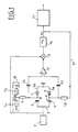
- Fig. 1 is an electrical diagram showing an embodiment of the measuring device according to the invention.
- Fig. 2 is a curve showing the shape of the electrical signal delivered at a characteristic point of the measuring device according to the invention.
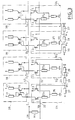
- Fig. 3 is an electrical diagram showing a characteristic detail of the linearization device according to the invention.
- Figs. 4A to 4E are curves illustrating the operating principle of the linearization circuit according to the invention.
- Fig. 5 illustrates an electrical diagram of a characteristic detail of the invention.
- Fig. 1 illustrates an exemplary embodiment of a measuring device adapted to determine the variations in capacity of a variable-type capacitor 1 .
- the capacitor 1 constitutes a capacitive sensor of mechanical quantities, such as force, pressure or acceleration.
- the capacitive sensor is in the form of a cantilever beam, made of a monolithic semiconductor substrate and comprising at least one flexible element of determined thickness, attached to a foot anchor on the substrate.
- the flexible element determines a movable armature of the variable capacitor, the fixed armature of which is formed by a conductive zone formed in the substrate.
- the measuring device aims to detect variations in the capacitance of the capacitor 1 , allowing the delivery of an electrical signal representative of the quantity measured.
- the measuring device comprises an oscillator 2 generating an alternating signal, for example of the square type, of frequency of the order of Megahertz and of amplitude of the order of a few volts.
- the measurement device comprises a detection bridge 3 formed by a first 3 a and a second 3 b branches connected to the oscillator 2 and to ground.
- the first branch 3 a is composed by the capacitor 1 connected in series with a diode 5 with variable capacity.
- the diode 5 is polarized so as to behave like a capacitor whose capacity is able to be controlled by a voltage.
- the anode of the diode 5 is connected, at a common point A , to an armature of the capacitor 1 .
- the second branch 3 b is formed by a capacitor 6 connected in series with a diode 7 with variable capacity identical to the diode 5 .
- the common point B between the capacitor 6 and the anode of the diode 7 , is connected, by means of a DC bias resistor 9 , to a DC bias circuit 10 of the point B and, consequently , of diode 7 , making it possible to fix the balance point of the detection bridge.
- the bias circuit 10 is capable of delivering a reference voltage Vref , preferably adjustable, and formed for example by a divider bridge composed of resistors 7 a , 7 b .
- variable voltage is chosen so that the amplitude of the signal, variable at points A , B , is small compared to that of the reference voltage.
- the capacitor 6 can also constitute a variable capacity sensor, allowing the differential detection of capacities.
- the common points A and B of the first and second branches 3 a , 3 b are connected to the input of a differential stage 12 , via, respectively, a link capacitor 13 , 14 adapted to cut the DC component of the signal from the detection bridge.
- the differential stage 12 is constituted by an amplifier whose non-inverting input is connected to the common point B , while the inverting input is connected to the point A.
- the amplifier 12 is connected to a circuit 15 for synchronous detection of the signal, receiving the synchronization information from the oscillator 2 .
- the synchronous detection circuit 15 produced in a known manner, is connected to a low-pass filter 16 of suitable cut-off frequency, of the order of, for example, 50 Hertz.
- the output of the filter 16 is connected to the common point A of the first branch, by a feedback line 17 in which is mounted a resistor 18 of continuous polarization of the diode 5 .
- the feedback from the detection bridge 3 at the branch which includes the variable capacity, ensures continuous rebalancing of the detection bridge.
- the signal Ve delivered by the filter 16 corresponds to the unbalance signal of the bridge which thus makes it possible to continuously measure the variation in the capacity of the variable capacitor 1 .
- the filter 16 is followed by a circuit 21 for linearization of the signal of imbalance of the bridge Ve , adapted to correct the linearity defect of the sensor 1 and of the diodes 5 and 7 .
- the linearization circuit 21 comprises at least one, and in the example illustrated in FIG. 3 , four differential threshold U1-U4 units, each comprising a first input 22 receiving the imbalance signal Ve and a second input 23 having a reference voltage Vr1 to Vr4 respectively.
- Each unit U1-U4 delivers, respectively, an output current I1-I4 whose law of variation comprises a part with zero slope, connected to a part with determined slope, via an angular point defined for the voltage of corresponding reference.
- At least one, and for example two differential units U1, U2 each deliver an output current I1, I2 whose law of variation comprises a part N with zero slope for a value of the imbalance signal Ve , lower than that of the voltage of reference Vr1, corresponding Vr2 , and a part P with determined slope, for a value of the signal Ve greater than that of the voltage Vr1, Vr2 which corresponds to the angular point of the curve.
- the linearization circuit can also include at least one and, in the example illustrated, two differential units U3, U4 delivering, in accordance with FIGS . 4C-4D , an output signal I3, I4 whose variation law includes a part with zero slope N for a value of the imbalance signal greater than that of the reference voltage Vr3, Vr4, and a part with determined slope P , for a value of the imbalance signal lower than that of the corresponding reference voltage.
- the flat part M of the curve, extending the part with a slope P is not used for the object of the invention.
- Fig. 3 illustrates an embodiment of differential threshold units U unix-U4 capable of delivering an output signal affecting the characteristics set out above.
- Each differential unit U1, U2 comprises a transistor T1 , of the NPN type, the base of which receives the imbalance signal Ve .
- the emitter of transistor T1 differential units U1, U2 is connected, via a resistor 251, 252, to the emitter of an NPN transistor T2.
- the emitter of transistor T2 is connected, via a resistor 26 , to ground, while the collector of this transistor T2 is connected to a bias voltage.
- the base of the transistor T2 of each unit U1, U2 receives the corresponding reference signal Vr1, Vr2 which is delivered, for example, by a voltage divider bridge formed by resistors 27 , 28 , 29 .
- the slope of the current variation curve I1, I2 ( fig. 4A, 4B ) is determined by the value R251- R252 of the corresponding resistance 251, 252 .
- the angular point of this curve is directly defined for the reference voltage Vr1, Vr2 .
- each differential unit U3, U4 comprises a transistor T3 whose base receives the corresponding reference signal Vr3, Vr4 which is delivered, for example, by a divider bridge 30, 31, 32 .
- the emitter of transistor T3 of differential units U un inclusive, U4 is connected to the emitter of a transistor T4 , via a resistor 333, 334 .
- the emitter of transistor T4 is connected to a resistor 35 connected to ground, while the collector of transistor T4 is connected to a bias voltage.
- the base of transistor T4 receives the imbalance signal Ve .
- the slope of the law of variation of the currents I3, I4 can therefore be adapted as a function of the choice of the value R333, R334 of the resistors 333, 334 .
- the angular point of this law is directly determined by the reference voltages Vr3, Vr4 .
- each differential unit U1- U4 is associated with a means 38 for combining the currents I1- I4 coming from the differential units, so as to obtain a resultant current I , image of all the currents delivered by the differential units.
- the combining means 38 each consist of a current mirror and are associated together to add the currents I1 to I4 and obtain a resulting current I , the law of variation of which is illustrated in FIG. 4E .
- each current mirror 38 comprises a PNP type transistor T5 , the collector of which is connected to its base and to the collector of the transistor T1 .
- the emitter of transistor T5 is provided with a bias resistor 41 , while the base of transistor T5 is connected to the base of a transistor T6 whose emitter is connected to a bias resistor 42 .
- the collector of transistor T6 is connected to a collector line 43 connected to the collectors of transistors T6 of the other current mirrors 38 . It should be noted that the choice of resistors 41 , 42 makes it possible to adjust the slope of the law of variation of the currents I1-I4.
- the linearization circuit according to the invention thus makes it possible to ensure linearization of an electrical signal, the law of variation of which exhibits inflections in the opposite direction, as this clearly appears in FIG. 2 .
- the linearization circuit according to the invention may generally comprise n differential units with threshold U , each associated with a combining means 38 .
- the number of differential units is chosen according to the linearization precision to be obtained.
- the type of differential units, used individually or in combination is determined according to the signal to be linearized.
- the linearization, carried out by the circuit can be adjusted by choosing suitable values for the resistances 251, 252, 333, 334, 41 and 42 , as well as for the reference voltages Vr .
- the linearization circuit according to the invention obviously has a limited cost, while presenting the possibility of analog signal adjustment.
- the measurement device as a whole namely the detection bridge and the linearization circuit, is formed from components which can be produced on an integrated circuit.
- the collector of transistor T6 is connected to the collector of a transistor T7 , the emitter of which is connected to ground via a resistor 44 .
- the base of the transistor T7 which is connected to its collector, is connected to the base of a transistor T8 , the emitter of which is connected to ground by means of a resistor 45 .
- the collector of transistor T8 is connected to the collector line 43 from which the currents I1-I4 are subtracted. It should be noted that the slope of the law of variation of the currents can be adapted as a function of the resistances 44 , 45 .
- the invention finds a particularly advantageous application for measuring the variations in capacitance of a capacitor forming a sensor of mechanical quantities, such as force, acceleration or pressure.
Landscapes
- Engineering & Computer Science (AREA)
- Power Engineering (AREA)
- Physics & Mathematics (AREA)
- General Physics & Mathematics (AREA)
- Transmission And Conversion Of Sensor Element Output (AREA)
- Measurement Of Resistance Or Impedance (AREA)
- Indication And Recording Devices For Special Purposes And Tariff Metering Devices (AREA)
- Measuring Fluid Pressure (AREA)
Abstract
Description
La présente invention concerne le domaine technique des dispositifs de mesure au sens général, adaptés pour déterminer les variations de capacité d'un condensateur à caractère variable.The present invention relates to the technical field of measuring devices in the general sense, adapted to determine the variations in capacity of a variable-type capacitor.
L'art antérieur a déjà proposé de nombreux dispositifs de mesure qui, par la détection des variations de capacité, permettent la délivrance d'un signal électrique représentant la grandeur mesurée. Un tel signal est destiné à être appliqué à des chaînes électroniques de traitement afin d'assurer, par exemple, des contrôles, mesures, régulation ou asservissement automatiques.The prior art has already proposed numerous measurement devices which, by detecting variations in capacity, allow the delivery of an electrical signal representing the quantity measured. Such a signal is intended to be applied to electronic processing chains in order to ensure, for example, automatic controls, measurements, regulation or control.
De tels dispositifs de mesure sont constitués classiquement par un circuit électrique appelé conditionneur, associé directement au capteur capacitif pour délivrer le signal électrique traduisant les variations de capacités du capteur, liées aux évolutions de la grandeur physique à mesurer. Ces dispositifs de mesure de la capacité d'un capteur comportent généralement aussi un circuit de linéarisation associé au conditionneur, pour permettre de corriger le défaut de linéarité du capteur ou éventuellement, également, du conditionneur utilisé, lorsque ce ou ces derniers présentent, dans leur domaine d'emploi, des écarts à la linéarité interdisant de considérer la sensibilité comme constante, en relation de la précision exigée des mesures. Le défaut de linéarité intervient, par exemple, lors de la mise en oeuvre d'un capteur capacitif constitué sous la forme d'une poutre en porte-à-faux comportant un élément sensible formant une armature mobile placée en relation de distance d'une armature fixe présentée par un support de fixation de l'élément sensible.Such measurement devices are conventionally constituted by an electrical circuit called a conditioner, associated directly with the capacitive sensor to deliver the electrical signal reflecting the variations in capacitances of the sensor, linked to changes in the physical quantity to be measured. These devices for measuring the capacity of a sensor generally also include a linearization circuit associated with the conditioner, in order to correct the defect in linearity of the sensor or possibly also of the conditioner used, when this or these present, in their field of use, deviations from linearity prohibiting the consideration of sensitivity as constant, in relation to the precision required of the measurements. The linearity defect occurs, for example, during the implementation of a capacitive sensor constituted in the form of a cantilever beam comprising a sensitive element forming a movable frame placed in distance relation of a fixed frame presented by a support for fixing the sensitive element.
Il doit tout d'abord être constaté que les conditionneurs actuellement utilisés mettent en oeuvre des composants interdisant leur intégration sur un circuit et se trouvent destinés à fonctionner dans une gamme de température très réduite.It must first be noted that the conditioners currently used use components prohibiting their integration on a circuit and are intended to operate in a very reduced temperature range.
Par ailleurs, un premier type de circuits de linéarisation fait appel à des techniques numériques de linéarisation nécessitant la mise en oeuvre d'un convertisseur analogique-numérique, une mémoire affectant une valeur mémorisée à chaque valeur du signal électrique utilisé comme adresse de la mémoire, et un convertisseur numérique-analogique. De mise en oeuvre simple et rapide, ces circuits de linéarisation sont peu économiques car la précision est directement liée à la capacité de la mémoire.In addition, a first type of linearization circuit uses digital linearization techniques requiring the use of an analog-digital converter, a memory assigning a stored value to each value of the electrical signal used as address of the memory, and a digital-to-analog converter. Simple and quick to implement, these linearization circuits are not very economical because the precision is directly linked to the capacity of the memory.
Un second type de circuits de linéarisation fait appel à des techniques analogiques mettant en oeuvre des diodes. L'utilisation de tels circuits est en pratique limitée à la linéarisation d'un signal électrique dont la courbe de variation présente une inflexion de sens prédéterminée et unique.A second type of linearization circuit uses analog techniques using diodes. The use of such circuits is in practice limited to the linearization of an electrical signal, the variation curve of which has an inflection of predetermined and unique direction.
Dans l'article de J.E. Sigdell "A Principle for Capacitance Measurement, Suitable for Linear Evaluation of Capacitance Transducers", IEEE Transations on Instrumentation and Measurement, Vol. 21, N°1, février 1972, est représenté le schéma électrique d'un dispositif de mesure de capacité comportant un oscillateur générant un signal alternatif appliqué à une diagonale d'un pont capacitif de détection incluant la capacité variable mesurée, et un amplificateur dont les entrées sont connectées à l'autre diagonale du pont capacitif (figure 12). La sortie de l'amplificateur est reliée à son entrée négative par une résistance de contre-réaction pour que l'amplificateur fonctionne en mode différentiel.In the article by J.E. Sigdell "A Principle for Capacitance Measurement, Suitable for Linear Evaluation of Capacitance Transducers", IEEE Transations on Instrumentation and Measurement, Vol. 21, No. 1, February 1972, is represented the electrical diagram of a capacity measurement device comprising an oscillator generating an alternating signal applied to a diagonal of a capacitive detection bridge including the measured variable capacity, and an amplifier whose the inputs are connected to the other diagonal of the capacitive bridge (figure 12). The output of the amplifier is connected to its negative input by a feedback resistance so that the amplifier operates in differential mode.
La présente invention vise donc à remédier aux inconvénients énoncés ci-dessus, en proposant un dispositif de mesure des variations de la capacité d'un condensateur, présentant une bonne insensibilité aux capacités parasites et aux perturbations électriques et autorisant sa miniaturisation sur un circuit intégré.The present invention therefore aims to remedy the drawbacks set out above, by proposing a device for measuring variations in the capacity of a capacitor, having good insensitivity to stray capacitances and electrical disturbances and allowing its miniaturization on an integrated circuit.
L'objet de l'invention vise aussi à offrir un dispositif de mesure adapté pour corriger le défaut de linéarité d'un signal électrique dont la loi de variation présente des inflexions de sens variées.The object of the invention also aims to provide a measuring device suitable for correcting the linearity defect of an electrical signal whose law of variation has inflections of various directions.
L'objet de l'invention vise, également, à proposer un dispositif de mesure qui, adapté pour corriger le défaut de linéarité intervenant entre le signal électrique délivré et les variations de la capacité du capteur, présente un coût relativement réduit.The object of the invention also aims to propose a measurement device which, adapted to correct the linearity defect occurring between the electrical signal delivered and the variations in the capacitance of the sensor, presents a relatively reduced cost.
L'invention propose ainsi un dispositif de mesure tel que défini dans la revendication 1.The invention thus provides a measuring device as defined in
Un mode de réalisation avantageux de l'invention, adapté pour linéariser le signal de déséquilibre du pont de détection, est défini dans la revendication 4.An advantageous embodiment of the invention, adapted to linearize the signal of imbalance of the detection bridge, is defined in
Diverses autres caractéristiques ressortent de la description faite ci-dessous en référence aux dessins annexés qui montrent, à titre d'exemples non limitatifs, des formes de réalisation de l'objet de l'invention.Various other characteristics will emerge from the description given below with reference to the appended drawings which show, by way of nonlimiting examples, embodiments of the subject of the invention.
La fig. 1 est un schéma électrique montrant un exemple de réalisation du dispositif de mesure selon l'invention. Fig. 1 is an electrical diagram showing an embodiment of the measuring device according to the invention.
La fig. 2 est une courbe montrant l'allure du signal électrique délivré en un point caractéristique du dispositif de mesure selon l'invention. Fig. 2 is a curve showing the shape of the electrical signal delivered at a characteristic point of the measuring device according to the invention.
La fig. 3 est un schéma électrique montrant un détail caractéristique du dispositif de linéarisation selon l'invention. Fig. 3 is an electrical diagram showing a characteristic detail of the linearization device according to the invention.
Les fig. 4A à 4E sont des courbes illustrant le principe de fonctionnement du circuit de linéarisation selon l'invention. Figs. 4A to 4E are curves illustrating the operating principle of the linearization circuit according to the invention.
La fig. 5 illustre un schéma électrique d'un détail caractéristique de l'invention. Fig. 5 illustrates an electrical diagram of a characteristic detail of the invention.
La fig. 1 illustre un exemple de réalisation d'un dispositif de mesure adapté pour déterminer les variations de capacité d'un condensateur 1 à caractère variable. Avantageusement, le condensateur 1 constitue un capteur capacitif de grandeurs mécaniques, telles que force, pression ou accélération. Selon un exemple préféré de réalisation, le capteur capacitif se présente sous la forme d'une poutre en porte-à-faux, réalisée en un substrat semi-conducteur monolithique et comportant au moins un élément flexible d'épaisseur déterminée, rattaché à un pied d'ancrage sur le substrat. L'élément flexible détermine une armature mobile du condensateur variable dont l'armature fixe est constituée par une zone conductrice formée dans le substrat. Fig. 1 illustrates an exemplary embodiment of a measuring device adapted to determine the variations in capacity of a variable-
Le dispositif de mesure selon l'invention vise à détecter les variations de capacité du condensateur 1, permettant la délivrance d'un signal électrique représentatif de la grandeur mesurée. A cet effet, le dispositif de mesure comporte un oscillateur 2 générant un signal alternatif par exemple du type carré, de fréquence de l'ordre du Megahertz et d'amplitude de l'ordre de quelques volts. Le dispositif de mesure comporte un pont de détection 3 formé par une première 3a et une seconde 3b branches reliées à l'oscillateur 2 et à la masse.The measuring device according to the invention aims to detect variations in the capacitance of the
La première branche 3a est composée par le condensateur 1 monté en série avec une diode 5 à capacité variable. La diode 5 est polarisée de manière à se comporter comme un condensateur dont la capacité est apte à être commandée par une tension. A cet effet, l'anode de la diode 5 est reliée, en un point commun A , à une armature du condensateur 1.The
La seconde branche 3b est formée par un condensateur 6 monté en série avec une diode 7 à capacité variable identique à la diode 5. Le point commun B , entre le condensateur 6 et l'anode de la diode 7, est relié, par l'intermédiaire d'une résistance 9 de polarisation en continu, à un circuit 10 de polarisation en continu du point B et, par suite, de la diode 7, permettant de fixer le point d'équilibre du pont de détection. Le circuit de polarisation 10 est apte à délivrer une tension de référence Vref, de préférence ajustable, et formé par exemple par un pont diviseur composé de résistances 7a , 7b .The
Il est à noter que la tension variable est choisie de manière que l'amplitude du signal, variable aux points A , B , soit faible par rapport à celle de la tension de référence. De plus, le condensateur 6 peut constituer aussi un capteur à capacité variable, permettant la détection différentielle de capacités.It should be noted that the variable voltage is chosen so that the amplitude of the signal, variable at points A , B , is small compared to that of the reference voltage. In addition, the
Les points communs A et B des première et seconde branches 3a , 3b , sont reliés à l'entrée d'un étage différentiel 12, par l'intermédiaire, respectivement, d'un condensateur de liaison 13, 14 adapté pour couper la composante continue du signal provenant du pont de détection. Avantageusement, l'étage différentiel 12 est constitué par un amplificateur dont l'entrée non inverseuse est reliée au point commun B , tandis que l'entrée inverseuse est reliée au point A .The common points A and B of the first and
L'amplificateur 12 est relié à un circuit 15 de détection synchrone du signal, recevant l'information de synchronisation à partir de l'oscillateur 2. Le circuit de détection synchrone 15, réalisé de manière connue, est connecté à un filtre passe-bas 16 de fréquence de coupure adaptée, de l'ordre de, par exemple, 50 Hertz. La sortie du filtre 16 est reliée au point commun A de la première branche, par une ligne de contre-réaction 17 dans laquelle est montée une résistance 18 de polarisation en continu de la diode 5. La contre-réaction du pont de détection 3, au niveau de la branche qui comporte la capacité variable, permet d'assurer un rééquilibrage continu du pont de détection. Ainsi, le signal Ve délivré par le filtre 16, tel qu'illustré à la fig. 2, correspond au signal de déséquilibre du pont qui permet ainsi de mesurer en continu la variation de la capacité du condensateur variable 1.The
Avantageusement, le filtre 16 est suivi par un circuit 21 de linéarisation du signal Ve de déséquilibre du pont, adapté pour corriger le défaut de linéarité du capteur 1 et des diodes 5 et 7. Le circuit de linéarisation 21, selon l'invention, comporte au moins une, et dans l'exemple illustré à la fig. 3, quatre unités U₁-U₄ différentielles à seuil, comportant chacune une première entrée 22 recevant le signal de déséquilibre Ve et une seconde entrée 23 présentant une tension de référence respectivement Vr₁ à Vr₄. Chaque unité U₁-U₄ délivre, respectivement, un courant de sortie I₁-I₄ dont la loi de variation comporte une partie à pente nulle, raccordée à une partie à pente déterminée, par l'intermédiaire d'un point anguleux défini pour la tension de référence correspondante.Advantageously, the
Tel que cela apparaît plus précisément aux fig. 4A et 4B, au moins une, et par exemple deux unités différentielles U₁, U₂, délivrent chacune un courant de sortie I₁, I₂ dont la loi de variation comprend une partie N à pente nulle pour une valeur du signal de déséquilibre Ve, inférieure à celle de la tension de référence Vr₁, Vr₂ correspondante, et une partie P à pente déterminée, pour une valeur du signal Ve supérieure à celle de la tension Vr₁, Vr₂ qui correspond au point anguleux de la courbe.As shown more precisely in Figs. 4A and 4B , at least one, and for example two differential units U₁, U₂ , each deliver an output current I₁, I₂ whose law of variation comprises a part N with zero slope for a value of the imbalance signal Ve , lower than that of the voltage of reference Vr₁, corresponding Vr₂ , and a part P with determined slope, for a value of the signal Ve greater than that of the voltage Vr₁, Vr₂ which corresponds to the angular point of the curve.
Avantageusement, le circuit de linéarisation peut comporter, également, au moins une et, dans l'exemple illustré, deux unités différentielles U₃, U₄ délivrant, conformément aux fig. 4C-4D, un signal de sortie I₃, I₄ dont la loi de variation comprend une partie à pente nulle N pour une valeur du signal de déséquilibre supérieure à celle de la tension de référence Vr₃, Vr₄, et une partie à pente déterminée P , pour une valeur du signal de déséquilibre inférieure à celle de la tension de référence correspondante. Il est à noter que la partie plane M de la courbe, prolongeant la partie à pente P , n'est pas utilisée pour l'objet de l'invention.Advantageously, the linearization circuit can also include at least one and, in the example illustrated, two differential units U₃, U₄ delivering, in accordance with FIGS . 4C-4D , an output signal I₃, I₄ whose variation law includes a part with zero slope N for a value of the imbalance signal greater than that of the reference voltage Vr₃, Vr₄, and a part with determined slope P , for a value of the imbalance signal lower than that of the corresponding reference voltage. It should be noted that the flat part M of the curve, extending the part with a slope P , is not used for the object of the invention.
La fig. 3 illustre un exemple de réalisation des unités différentielles à seuil U₁-U₄ aptes à délivrer un signal de sortie affectant les caractéristiques énoncées ci-dessus. Chaque unité différentielle U₁, U₂ comporte un transistor T₁, du type NPN, dont la base reçoit le signal de déséquilibre Ve. L'émetteur du transistor T₁ des unités différentielles U₁, U₂ est connecté, par l'intermédiaire d'une résistance 25₁, 25₂, à l'émetteur d'un transistor T₂ du type NPN. L'émetteur du transistor T₂ est connecté, par l'intermédiaire d'une résistance 26, à la masse, tandis que le collecteur de ce transistor T₂ est reliée à une tension de polarisation. La base du transistor T₂ de chaque unité U₁, U₂ reçoit le signal de référence Vr₁, Vr₂ correspondant qui est délivré, par exemple, par un pont diviseur de tension formé par des résistances 27, 28, 29. Fig. 3 illustrates an embodiment of differential threshold units U unités-U₄ capable of delivering an output signal affecting the characteristics set out above. Each differential unit U₁, U₂ comprises a transistor T₁ , of the NPN type, the base of which receives the imbalance signal Ve . The emitter of transistor T₁ differential units U₁, U₂ is connected, via a
Le fonctionnement de chaque unité différentielle découle directement de la description établie ci-dessus. Si le signal Ve présente une valeur de tension inférieure à une tension de référence Vr₁, Vr₂, le transistor T₁ correspondant est bloqué, de sorte que le courant I₁, I₂, sortant du collecteur du transistor, est nul. Si la tension Ve présente une valeur supérieure à une tension de référence Vr₁, Vr₂, le collecteur du transistor T₁ débite un courant tel que :![]()
et :![]()
![]()
and: ![]()
Il est à noter que la pente de la courbe de variation du courant I₁, I₂ (fig. 4A, 4B) est déterminée par la valeur R25₁- R25₂ de la résistance correspondante 25₁, 25₂. De plus, le point anguleux de cette courbe est directement défini pour la tension de référence Vr₁, Vr₂.It should be noted that the slope of the current variation curve I₁, I₂ ( fig. 4A, 4B ) is determined by the value R25₁- R25₂ of the
Tel que cela apparaît plus précisément à la fig. 3, chaque unité différentielle U₃, U₄ comporte un transistor T₃ dont la base reçoit le signal de référence Vr₃, Vr₄ correspondant qui est délivré, par exemple, par un pont diviseur 30, 31, 32. L'émetteur du transistor T₃ des unités différentielles U₃, U₄ est relié à l'émetteur d'un transistor T₄, par l'intermédiaire d'une résistance 33₃, 33₄. L'émetteur du transistor T₄ est relié à une résistance 35 connectée à la masse, tandis que le collecteur du transistor T₄ est relié à une tension de polarisation. La base du transistor T₄ reçoit le signal de déséquilibre Ve.As shown more precisely in fig. 3 , each differential unit U₃, U₄ comprises a transistor T₃ whose base receives the corresponding reference signal Vr₃, Vr₄ which is delivered, for example, by a
Si le signal Ve présente une valeur de tension supérieure à la tension de référence Vr₃, Vr₄, le transistor T₃ est bloqué, de sorte que le courant I₃, I₄, sortant du collecteur du transistor T₃, est nul (fig. 4C, 4D). Si la tension Ve présente une valeur inférieure à celle de la tension de référence Vr₃, Vr₄, le transistor T₃ est conducteur et débite un courant :![]()
et :![]()
![]()
and: ![]()
La pente de la loi de variation des courants I₃, I₄ peut donc être adaptée en fonction du choix de la valeur R33₃, R33₄ des résistances 33₃, 33₄. De même, le point anguleux de cette loi se trouve directement déterminé par les tensions de référence Vr₃, Vr₄.The slope of the law of variation of the currents I₃, I₄ can therefore be adapted as a function of the choice of the value R33₃, R33₄ of the
Tel que cela apparaît plus précisément à la fig. 3, chaque unité différentielle U₁- U₄ est associée à un moyen 38 de combinaison des courants I₁- I₄ issus des unités différentielles, de manière à obtenir un courant résultant I , image de tous les courants délivrés par les unités différentielles. Dans l'exemple illustré, les moyens de combinaison 38 sont constitués chacun par un miroir de courant et se trouvent associés ensemble pour additionner les courants I₁ à I₄ et obtenir un courant résultant I dont la loi de variation est illustrée à la fig. 4E.As shown more precisely in fig. 3 , each differential unit U₁- U₄ is associated with a
A titre d'exemple, chaque miroir de courant 38 comporte un transistor T₅ de type PNP dont le collecteur est relié à sa base et au collecteur du transistor T₁. L'émetteur du transistor T₅ est pourvu d'une résistance 41 de polarisation, tandis que la base du transistor T₅ est reliée à la base d'un transistor T₆ dont l'émetteur est connecté à une résistance de polarisation 42. Le collecteur du transistor T₆ est relié à une ligne collectrice 43 connectée aux collecteurs des transistors T₆ des autres miroirs de courant 38. Il est à noter que le choix des résistances 41, 42 permet de régler la pente de la loi de variation des courants I₁-I₄. By way of example, each
Le courant résultant I peut alors traverser une résistance Rs de manière à obtenir, en combinaison avec le signal Ve, un signal de sortie linéarisé Vs, tel que :![]()
![]()
Le circuit de linéarisation selon l'invention permet ainsi d'assurer une linéarisation d'un signal électrique dont la loi de variation présente des inflexions de sens contraire, tel que cela apparaît clairement à la fig. 2.The linearization circuit according to the invention thus makes it possible to ensure linearization of an electrical signal, the law of variation of which exhibits inflections in the opposite direction, as this clearly appears in FIG. 2 .
Bien entendu, le circuit de linéarisation selon l'invention peut comporter, d'une manière générale, n unités différentielles à seuil U , associées chacune à un moyen de combinaison 38. Le nombre d'unités différentielles est choisi en fonction de la précision de linéarisation à obtenir. De plus, le type d'unités différentielles, utilisées individuellement ou en combinaison, est déterminé en fonction du signal à linéariser. La linéarisation, effectuée par le circuit, peut être réglée en choisissant des valeurs adaptées pour les résistances 25₁, 25₂, 33₃, 33₄, 41 et 42, ainsi que pour les tensions de référence Vr. Le circuit de linéarisation selon l'invention présente, manifestement, un coût limité, tout en présentant une possibilité de réglage analogique du signal.Of course, the linearization circuit according to the invention may generally comprise n differential units with threshold U , each associated with a combining means 38 . The number of differential units is chosen according to the linearization precision to be obtained. In addition, the type of differential units, used individually or in combination, is determined according to the signal to be linearized. The linearization, carried out by the circuit, can be adjusted by choosing suitable values for the
De plus, il est à noter que le dispositif de mesure dans son ensemble, à savoir le pont de détection et le circuit de linéarisation, est formé à partir de composants pouvant être réalisés sur un circuit intégré.In addition, it should be noted that the measurement device as a whole, namely the detection bridge and the linearization circuit, is formed from components which can be produced on an integrated circuit.
Il doit être considéré, par ailleurs, que le signe de la pente du courant résultant I peut être modifiée si les moyens de combinaison 38 assurent, non pas une addition, mais une soustraction des courants délivrés par les unités différentielles à seuil. A cet effet, tel que cela apparaît plus clairement à la fig. 5, le collecteur du transistor T₆ est relié au collecteur d'un transistor T₇ dont l'émetteur est relié à la masse par l'intermédiaire d'une résistance 44. La base du transistor T₇, qui est relié à son collecteur, est connectée à la base d'un transistor T₈ dont l'émetteur est relié à la masse grâce à une résistance 45. Le collecteur du transistor T₈ est relié à la ligne collectrice 43 à partir de laquelle les courants I₁-I₄ sont soustraits. Il est à noter que la pente de la loi de variation des courants peut être adaptée en fonction des résistances 44, 45.It should also be considered that the sign of the slope of the resulting current I can be modified if the combining means 38 ensure, not an addition, but a subtraction of the currents delivered by the differential differential units. To this end, as it appears more clearly in FIG. 5 , the collector of transistor T₆ is connected to the collector of a transistor T₇ , the emitter of which is connected to ground via a
L'invention trouve une application particulièrement avantageuse pour la mesure des variations de capacité d'un condensateur formant un capteur de grandeurs mécaniques, telles que force, accélération ou pression.The invention finds a particularly advantageous application for measuring the variations in capacitance of a capacitor forming a sensor of mechanical quantities, such as force, acceleration or pressure.
Claims (13)
- A circuit for measuring variations in the capacitance of a variable capacitor constituting, in particular, a sensor, comprising an oscillator (2) generating an alternating signal, a detection bridge (3) comprising first and second branches (3a, 3b) connected to the oscillator, the first branch including a variable capacitor (1) connected in series with another capacitive element (5), while the second branch comprises a capacitor (6) connected in series with another capacitive element (7), and a differential stage (12), each input of which is connected to the common point of a respective branch located between a capacitor and said corresponding capacitive element, characterized in that said capacitive elements are variable capacitance diodes (5,7), in that a DC bias circuit (10) is provided for biasing the common point (B) of the second branch so as to fix the equilibrium point of the detection bridge, in that the differential stage (12) is followed by synchronous detection and low-pass filtering means (15,16) connected to the oscillator and delivering a signal (Ve) representing the unbalance of the detection bridge, and in that the unbalance signal (Ve) is injected by a feedback line (17) to the common point (A) of the first branch to continuously rebalance the detection bridge and consequently to continuously measure the variation in the capacitance of the variable capacitor.
- A circuit according to claim 1, characterized in that each input of the differential stage (12) is connected to the common point of a branch by means of a coupling capacitor (13,14).
- A circuit according to claim 1, characterized in that the common points of the branches are connected respectively to the bias circuit (10) and to the feedback line (17) by means of bias resistors (9,18) for the variable capacitance diodes.
- A circuit according to claim 1, characterized in that the lowpass filter is connected to a linearization circuit (21) for the unbalance signal of the detection bridge, the linearization circuit comprising:
n threshold differential units (U1,..., Un) each receiving as inputs the unbalance signal and a respective reference voltage (Vr), and each delivering an output signal in the form of a current (I₁,...,In) which varies in a manner that includes a portion (N) of zero slope connected to a portion (P) of determined slope by means of an angle point defined by the reference voltage; and
n means (38) for combining the currents from the differential units, thereby obtaining a resultant signal (I) having multiple angle points which, when combined with the unbalance signal, enables it to be linearized. - A circuit according to claim 4, characterized in that at least one differential unit delivers an output current (I₁, I₂,...) whose variation includes a zero slope portion (N) for any value of the unbalance signal (Ve) below the reference voltage (Vr), and a determined slope portion (P) for any value of the unbalance signal (Ve) greater than the reference voltage.
- A circuit according to claim 4 or 5, characterized in that at least one of the differential units delivers an output current (I₁, I₂,...) which varies in a manner that includes a zero slope portion (N) for any value of the unbalance signal (Ve) greater than the reference voltage, and a determined slope portion (P) for any value of the unbalance signal (Ve) less than the reference voltage (Vr).
- A circuit according to claim 5, characterized in that each differential unit is constituted by a first transitor (T₁) having a base connected to the reference voltage and an emitter connected via a resistor (25₁, 25₂,...) to the emitter of a second transistor (T₂) whose base receives the unbalance signal (Ve), while its collector delivers the output current (I₁, I₂,...)
- A circuit according to claim 6, characterized in that each differential unit is constituted by a first transistor (T₃) having a base receiving the unbalance signal and an emitter which is connected via a resistor (33₃, 33₄,...) to the emitter of a second transistor (T₄) whose base is connected to the reference voltage, whereas its collector delivers the output current (I₃, I₄,...).
- A circuit according to claim 7 or 8, characterized in that the emitter resistors (25₁, 25₂,..., 33₃, 33₄,..., 41, 42) determine the slope (P) of the variation in the output current of the analog units.
- A circuit according to claim 4, characterized in that each combination means (38) is formed by a current mirror.
- A circuit according to claim 10, characterized in that the current mirrors (38) subtract the output currents delivered by the analog units.
- A circuit according to claim 10, characterized in that the current mirrors (38) add the output currents delivered by the analog units.
- A circuit according to claim 1, characterized in that the capacitor (6) of the second branch is variable in order to provide differential capacitance detection.
Applications Claiming Priority (3)
| Application Number | Priority Date | Filing Date | Title |
|---|---|---|---|
| FR8917551A FR2656698B1 (en) | 1989-12-29 | 1989-12-29 | DEVICE FOR MEASURING VARIATIONS IN THE CAPACITY OF A CAPACITOR FORMING, IN PARTICULAR, A SENSOR. |
| FR8917551 | 1989-12-29 | ||
| PCT/FR1990/000961 WO1991009812A2 (en) | 1989-12-29 | 1990-12-28 | Device for measuring the variations in the capacitance of a capacitor, particularly a detector |
Publications (2)
| Publication Number | Publication Date |
|---|---|
| EP0510061A1 EP0510061A1 (en) | 1992-10-28 |
| EP0510061B1 true EP0510061B1 (en) | 1994-04-20 |
Family
ID=9389226
Family Applications (1)
| Application Number | Title | Priority Date | Filing Date |
|---|---|---|---|
| EP91902297A Expired - Lifetime EP0510061B1 (en) | 1989-12-29 | 1991-07-25 | Device for measuring the variations in the capacitance of a capacitor, particularly a detector |
Country Status (6)
| Country | Link |
|---|---|
| US (1) | US5311140A (en) |
| EP (1) | EP0510061B1 (en) |
| DE (1) | DE69008363T2 (en) |
| ES (1) | ES2051118T3 (en) |
| FR (1) | FR2656698B1 (en) |
| WO (1) | WO1991009812A2 (en) |
Families Citing this family (20)
| Publication number | Priority date | Publication date | Assignee | Title |
|---|---|---|---|---|
| JP3139305B2 (en) * | 1994-08-24 | 2001-02-26 | 株式会社村田製作所 | Capacitive acceleration sensor |
| AT401826B (en) * | 1995-06-01 | 1996-12-27 | Peter Ing Klementschitz | MEASURING PROCEDURE |
| US5659195A (en) * | 1995-06-08 | 1997-08-19 | The Regents Of The University Of California | CMOS integrated microsensor with a precision measurement circuit |
| DE19528384C2 (en) * | 1995-08-02 | 1999-09-30 | Ulrich Pok | Capacitive measuring device for continuous level control for media with different dielectric constants |
| US5808198A (en) * | 1997-05-19 | 1998-09-15 | The Charles Stark Draper Laboratory, Inc. | RF balanced capacitive vibration sensor system |
| US20040099061A1 (en) * | 1997-12-22 | 2004-05-27 | Mks Instruments | Pressure sensor for detecting small pressure differences and low pressures |
| US6366099B1 (en) | 1999-12-21 | 2002-04-02 | Conrad Technologies, Inc. | Differential capacitance sampler |
| US7194390B1 (en) * | 2000-03-31 | 2007-03-20 | United States Of America As Represented By The Secretary Of The Navy | Predictor of minimal noise figure for wideband amplifier |
| US6622092B1 (en) | 2000-03-31 | 2003-09-16 | The United States Of America As Represented By The Secretary Of The Navy | Predictor for optimal broadband impedance matching |
| FR2818676B1 (en) * | 2000-12-27 | 2003-03-07 | Freyssinet Int Stup | METHOD FOR DISASSEMBLING A PRE-STRESS CABLE AND DEVICE FOR IMPLEMENTING THE SAME |
| US20030121332A1 (en) * | 2001-12-21 | 2003-07-03 | Mathew Santhi E. | Pressure transducer with dual slope output |
| US6993973B2 (en) * | 2003-05-16 | 2006-02-07 | Mks Instruments, Inc. | Contaminant deposition control baffle for a capacitive pressure transducer |
| US7327275B2 (en) | 2004-02-02 | 2008-02-05 | Gecko Alliance Group Inc. | Bathing system controller having abnormal operational condition identification capabilities |
| US7201057B2 (en) * | 2004-09-30 | 2007-04-10 | Mks Instruments, Inc. | High-temperature reduced size manometer |
| US7141447B2 (en) * | 2004-10-07 | 2006-11-28 | Mks Instruments, Inc. | Method of forming a seal between a housing and a diaphragm of a capacitance sensor |
| US7137301B2 (en) * | 2004-10-07 | 2006-11-21 | Mks Instruments, Inc. | Method and apparatus for forming a reference pressure within a chamber of a capacitance sensor |
| US7368923B2 (en) * | 2005-12-22 | 2008-05-06 | Honeywell International Inc. | Time interval trimmed differential capacitance sensor |
| US9063067B1 (en) | 2010-11-17 | 2015-06-23 | Alvin P. Schmitt | Moisture sensing devices |
| EP3074763A1 (en) | 2013-11-25 | 2016-10-05 | Oil States Industries, Inc. | Method and system for health monitoring of composite elastomeric flexible elements |
| GB2615799A (en) * | 2022-02-18 | 2023-08-23 | Weiner Nicholas | Impedance sensor |
Family Cites Families (5)
| Publication number | Priority date | Publication date | Assignee | Title |
|---|---|---|---|---|
| FR2337346A1 (en) * | 1975-12-30 | 1977-07-29 | Onera (Off Nat Aerospatiale) | CAPACITY MEASUREMENT BRIDGE |
| US4241303A (en) * | 1979-01-17 | 1980-12-23 | The Babcock & Wilcox Company | Linearization circuit |
| US4673869A (en) * | 1985-02-13 | 1987-06-16 | Phillips Petroleum Company | Dielectric constant detector capacitance matching |
| US4684886A (en) * | 1985-05-17 | 1987-08-04 | Doyle James H | Automatic equalizer |
| JPS62168408A (en) * | 1985-11-21 | 1987-07-24 | Shimadzu Corp | Automatic resonance and matching device of antenna circuit for mri device |
-
1989
- 1989-12-29 FR FR8917551A patent/FR2656698B1/en not_active Expired - Fee Related
-
1990
- 1990-12-28 DE DE69008363T patent/DE69008363T2/en not_active Expired - Fee Related
- 1990-12-28 WO PCT/FR1990/000961 patent/WO1991009812A2/en active IP Right Grant
- 1990-12-28 US US07/924,049 patent/US5311140A/en not_active Expired - Fee Related
- 1990-12-28 ES ES91902297T patent/ES2051118T3/en not_active Expired - Lifetime
-
1991
- 1991-07-25 EP EP91902297A patent/EP0510061B1/en not_active Expired - Lifetime
Non-Patent Citations (2)
| Title |
|---|
| IEEE Transactions on Instrumentation and Measurement, Vol. 21, No. 1, Fevrier 1972, New York US, J.E. Sigdell: "A principle for capacitance measurement, suitable for linear evaluation of capacitance transducers", pages 60-61 * |
| PATENT ABSTRACTS OF JAPAN, Vol. 12, No. 7 (E-571), 9 janvier 1988, & JP-A-6 216 84 08 * |
Also Published As
| Publication number | Publication date |
|---|---|
| EP0510061A1 (en) | 1992-10-28 |
| WO1991009812A2 (en) | 1991-07-11 |
| WO1991009812A3 (en) | 1991-08-22 |
| US5311140A (en) | 1994-05-10 |
| DE69008363D1 (en) | 1994-05-26 |
| ES2051118T3 (en) | 1994-06-01 |
| DE69008363T2 (en) | 1994-11-17 |
| FR2656698B1 (en) | 1992-05-07 |
| FR2656698A1 (en) | 1991-07-05 |
Similar Documents
| Publication | Publication Date | Title |
|---|---|---|
| EP0510061B1 (en) | Device for measuring the variations in the capacitance of a capacitor, particularly a detector | |
| EP0285478B1 (en) | Circuit for converting analogous signals into digital signals | |
| EP2541213B1 (en) | Method for reducing non-linearity during the measurement of a physical parameter and electronic circuit for implementing the same | |
| CA2831353C (en) | Method and system for detecting a short-circuit affecting a sensor | |
| CH628993A5 (en) | APPARATUS FOR DETECTING AN EXTERNAL MAGNETIC FIELD. | |
| EP2726832B1 (en) | Resistive device comprising a silcon-nanowire-comprising strain gauge and method for optimizing the electrical consumption of such a device | |
| EP0280632B1 (en) | Electronic angle-measuring device | |
| WO2012156016A1 (en) | Differential voltage measurement | |
| EP2662667A1 (en) | Method for measuring a physical parameter and electronic circuit to interface with a capacitive sensor for implementing same | |
| EP2887014A1 (en) | Electronic circuit for measuring the speed of rotation in a MEMS gyroscope and method for operating the same | |
| EP0990128B1 (en) | Pressure sensor with compensation for null shift non-linearity at very low temperatures | |
| EP2694920B1 (en) | Method of correction of measurement of tension at the terminals of a sensor | |
| FR2735868A1 (en) | DEVICE FOR MEASURING AN ANGULAR SPEED | |
| FR2764068A1 (en) | CIRCUIT FOR MEASURING THE CURRENT IN THE ELECTRODES OF A CERAMIC GAS SENSOR | |
| FR2908508A1 (en) | Electronic device e.g. electrostatic type die cast membrane keyboard for e.g. measuring physical unit, has determining unit to determine derivative signal from evolution of output signal of phase comparison component | |
| FR2496894A1 (en) | CIRCUIT FOR CONTROLLING AN ELECTROSTATIC ACCELEROMETER | |
| EP0796421B1 (en) | Filtering device particularly for a fuel gauge of a motor vehicle | |
| EP1691203B1 (en) | Electronic circuit comprising a low noise capacitive sensor and accelerometer being equiped with such a circuit | |
| WO2009103900A2 (en) | Method of correcting the gain of a capacitive unit and device for implementing same | |
| EP0266282B1 (en) | Attitude alarm | |
| FR2656699A1 (en) | ANALOG LINEARIZATION CIRCUIT. | |
| FR2796725A1 (en) | Measuring sensitivity of Hall effect sensor by supplying calibrating coil with equal positive and negative pulses at a much higher frequency than field to be measured and processing sensor output | |
| FR2659447A1 (en) | Force measurement device comprising a temperature-compensated piezo-resistive transducer | |
| FR2565353A1 (en) | METHOD FOR MEASURING CAPACITIES, ESPECIALLY LOW CAPACITIES, IN WHICH TWO REFERENCE CAPACITIES ARE USED | |
| FR3123452A1 (en) | Isolated floating voltage measurement circuit |
Legal Events
| Date | Code | Title | Description |
|---|---|---|---|
| PUAI | Public reference made under article 153(3) epc to a published international application that has entered the european phase |
Free format text: ORIGINAL CODE: 0009012 |
|
| 17P | Request for examination filed |
Effective date: 19920710 |
|
| AK | Designated contracting states |
Kind code of ref document: A1 Designated state(s): BE CH DE ES GB IT LI NL SE |
|
| 17Q | First examination report despatched |
Effective date: 19921120 |
|
| RAP1 | Party data changed (applicant data changed or rights of an application transferred) |
Owner name: SOCIETE D'APPLICATIONS GENERALES D'ELECTRICITE ET |
|
| GRAA | (expected) grant |
Free format text: ORIGINAL CODE: 0009210 |
|
| AK | Designated contracting states |
Kind code of ref document: B1 Designated state(s): BE CH DE ES GB IT LI NL SE |
|
| REF | Corresponds to: |
Ref document number: 69008363 Country of ref document: DE Date of ref document: 19940526 |
|
| REG | Reference to a national code |
Ref country code: ES Ref legal event code: FG2A Ref document number: 2051118 Country of ref document: ES Kind code of ref document: T3 |
|
| GBT | Gb: translation of ep patent filed (gb section 77(6)(a)/1977) |
Effective date: 19940505 |
|
| ITF | It: translation for a ep patent filed | ||
| EAL | Se: european patent in force in sweden |
Ref document number: 91902297.0 |
|
| PLBE | No opposition filed within time limit |
Free format text: ORIGINAL CODE: 0009261 |
|
| STAA | Information on the status of an ep patent application or granted ep patent |
Free format text: STATUS: NO OPPOSITION FILED WITHIN TIME LIMIT |
|
| 26N | No opposition filed | ||
| PGFP | Annual fee paid to national office [announced via postgrant information from national office to epo] |
Ref country code: NL Payment date: 19951117 Year of fee payment: 6 |
|
| PGFP | Annual fee paid to national office [announced via postgrant information from national office to epo] |
Ref country code: ES Payment date: 19951128 Year of fee payment: 6 |
|
| PGFP | Annual fee paid to national office [announced via postgrant information from national office to epo] |
Ref country code: SE Payment date: 19951218 Year of fee payment: 6 |
|
| PGFP | Annual fee paid to national office [announced via postgrant information from national office to epo] |
Ref country code: GB Payment date: 19951222 Year of fee payment: 6 |
|
| PGFP | Annual fee paid to national office [announced via postgrant information from national office to epo] |
Ref country code: CH Payment date: 19951227 Year of fee payment: 6 |
|
| PGFP | Annual fee paid to national office [announced via postgrant information from national office to epo] |
Ref country code: BE Payment date: 19960117 Year of fee payment: 6 |
|
| PGFP | Annual fee paid to national office [announced via postgrant information from national office to epo] |
Ref country code: DE Payment date: 19960129 Year of fee payment: 6 |
|
| PG25 | Lapsed in a contracting state [announced via postgrant information from national office to epo] |
Ref country code: GB Effective date: 19961228 |
|
| PG25 | Lapsed in a contracting state [announced via postgrant information from national office to epo] |
Ref country code: SE Effective date: 19961229 |
|
| PG25 | Lapsed in a contracting state [announced via postgrant information from national office to epo] |
Ref country code: ES Free format text: LAPSE BECAUSE OF EXPIRATION OF PROTECTION Effective date: 19961230 |
|
| PG25 | Lapsed in a contracting state [announced via postgrant information from national office to epo] |
Ref country code: LI Effective date: 19961231 Ref country code: CH Effective date: 19961231 Ref country code: BE Effective date: 19961231 |
|
| BERE | Be: lapsed |
Owner name: SOC. D'APPLICATIONS GENERALES D'ELECTRICITE ET DE Effective date: 19961231 |
|
| PG25 | Lapsed in a contracting state [announced via postgrant information from national office to epo] |
Ref country code: NL Effective date: 19970701 |
|
| REG | Reference to a national code |
Ref country code: CH Ref legal event code: PL |
|
| GBPC | Gb: european patent ceased through non-payment of renewal fee |
Effective date: 19961228 |
|
| NLV4 | Nl: lapsed or anulled due to non-payment of the annual fee |
Effective date: 19970701 |
|
| PG25 | Lapsed in a contracting state [announced via postgrant information from national office to epo] |
Ref country code: DE Effective date: 19970902 |
|
| EUG | Se: european patent has lapsed |
Ref document number: 91902297.0 |
|
| REG | Reference to a national code |
Ref country code: ES Ref legal event code: FD2A Effective date: 20010201 |
|
| PG25 | Lapsed in a contracting state [announced via postgrant information from national office to epo] |
Ref country code: IT Free format text: LAPSE BECAUSE OF NON-PAYMENT OF DUE FEES;WARNING: LAPSES OF ITALIAN PATENTS WITH EFFECTIVE DATE BEFORE 2007 MAY HAVE OCCURRED AT ANY TIME BEFORE 2007. THE CORRECT EFFECTIVE DATE MAY BE DIFFERENT FROM THE ONE RECORDED. Effective date: 20051228 |