EP2722904A2 - Using stress reduction barrier sub-layers in a semiconductor die - Google Patents
Using stress reduction barrier sub-layers in a semiconductor die Download PDFInfo
- Publication number
- EP2722904A2 EP2722904A2 EP13180791.9A EP13180791A EP2722904A2 EP 2722904 A2 EP2722904 A2 EP 2722904A2 EP 13180791 A EP13180791 A EP 13180791A EP 2722904 A2 EP2722904 A2 EP 2722904A2
- Authority
- EP
- European Patent Office
- Prior art keywords
- sub
- layers
- layer
- semiconductor die
- primary conduction
- Prior art date
- Legal status (The legal status is an assumption and is not a legal conclusion. Google has not performed a legal analysis and makes no representation as to the accuracy of the status listed.)
- Pending
Links
Images




Classifications
-
- H—ELECTRICITY
- H10—SEMICONDUCTOR DEVICES; ELECTRIC SOLID-STATE DEVICES NOT OTHERWISE PROVIDED FOR
- H10W—GENERIC PACKAGES, INTERCONNECTIONS, CONNECTORS OR OTHER CONSTRUCTIONAL DETAILS OF DEVICES COVERED BY CLASS H10
- H10W20/00—Interconnections in chips, wafers or substrates
- H10W20/40—Interconnections external to wafers or substrates, e.g. back-end-of-line [BEOL] metallisations or vias connecting to gate electrodes
- H10W20/495—Capacitive arrangements or effects of, or between wiring layers
- H10W20/496—Capacitor integral with wiring layers
-
- C—CHEMISTRY; METALLURGY
- C23—COATING METALLIC MATERIAL; COATING MATERIAL WITH METALLIC MATERIAL; CHEMICAL SURFACE TREATMENT; DIFFUSION TREATMENT OF METALLIC MATERIAL; COATING BY VACUUM EVAPORATION, BY SPUTTERING, BY ION IMPLANTATION OR BY CHEMICAL VAPOUR DEPOSITION, IN GENERAL; INHIBITING CORROSION OF METALLIC MATERIAL OR INCRUSTATION IN GENERAL
- C23C—COATING METALLIC MATERIAL; COATING MATERIAL WITH METALLIC MATERIAL; SURFACE TREATMENT OF METALLIC MATERIAL BY DIFFUSION INTO THE SURFACE, BY CHEMICAL CONVERSION OR SUBSTITUTION; COATING BY VACUUM EVAPORATION, BY SPUTTERING, BY ION IMPLANTATION OR BY CHEMICAL VAPOUR DEPOSITION, IN GENERAL
- C23C28/00—Coating for obtaining at least two superposed coatings either by methods not provided for in a single one of groups C23C2/00 - C23C26/00 or by combinations of methods provided for in subclasses C23C and C25C or C25D
- C23C28/02—Coating for obtaining at least two superposed coatings either by methods not provided for in a single one of groups C23C2/00 - C23C26/00 or by combinations of methods provided for in subclasses C23C and C25C or C25D only coatings only including layers of metallic material
- C23C28/023—Coating for obtaining at least two superposed coatings either by methods not provided for in a single one of groups C23C2/00 - C23C26/00 or by combinations of methods provided for in subclasses C23C and C25C or C25D only coatings only including layers of metallic material only coatings of metal elements only
-
- C—CHEMISTRY; METALLURGY
- C23—COATING METALLIC MATERIAL; COATING MATERIAL WITH METALLIC MATERIAL; CHEMICAL SURFACE TREATMENT; DIFFUSION TREATMENT OF METALLIC MATERIAL; COATING BY VACUUM EVAPORATION, BY SPUTTERING, BY ION IMPLANTATION OR BY CHEMICAL VAPOUR DEPOSITION, IN GENERAL; INHIBITING CORROSION OF METALLIC MATERIAL OR INCRUSTATION IN GENERAL
- C23C—COATING METALLIC MATERIAL; COATING MATERIAL WITH METALLIC MATERIAL; SURFACE TREATMENT OF METALLIC MATERIAL BY DIFFUSION INTO THE SURFACE, BY CHEMICAL CONVERSION OR SUBSTITUTION; COATING BY VACUUM EVAPORATION, BY SPUTTERING, BY ION IMPLANTATION OR BY CHEMICAL VAPOUR DEPOSITION, IN GENERAL
- C23C28/00—Coating for obtaining at least two superposed coatings either by methods not provided for in a single one of groups C23C2/00 - C23C26/00 or by combinations of methods provided for in subclasses C23C and C25C or C25D
- C23C28/40—Coatings including alternating layers following a pattern, a periodic or defined repetition
- C23C28/42—Coatings including alternating layers following a pattern, a periodic or defined repetition characterized by the composition of the alternating layers
-
- H—ELECTRICITY
- H10—SEMICONDUCTOR DEVICES; ELECTRIC SOLID-STATE DEVICES NOT OTHERWISE PROVIDED FOR
- H10D—INORGANIC ELECTRIC SEMICONDUCTOR DEVICES
- H10D1/00—Resistors, capacitors or inductors
- H10D1/60—Capacitors
- H10D1/68—Capacitors having no potential barriers
- H10D1/692—Electrodes
- H10D1/694—Electrodes comprising noble metals or noble metal oxides
-
- H—ELECTRICITY
- H10—SEMICONDUCTOR DEVICES; ELECTRIC SOLID-STATE DEVICES NOT OTHERWISE PROVIDED FOR
- H10D—INORGANIC ELECTRIC SEMICONDUCTOR DEVICES
- H10D1/00—Resistors, capacitors or inductors
- H10D1/60—Capacitors
- H10D1/68—Capacitors having no potential barriers
- H10D1/692—Electrodes
- H10D1/696—Electrodes comprising multiple layers, e.g. comprising a barrier layer and a metal layer
-
- H—ELECTRICITY
- H10—SEMICONDUCTOR DEVICES; ELECTRIC SOLID-STATE DEVICES NOT OTHERWISE PROVIDED FOR
- H10W—GENERIC PACKAGES, INTERCONNECTIONS, CONNECTORS OR OTHER CONSTRUCTIONAL DETAILS OF DEVICES COVERED BY CLASS H10
- H10W20/00—Interconnections in chips, wafers or substrates
- H10W20/40—Interconnections external to wafers or substrates, e.g. back-end-of-line [BEOL] metallisations or vias connecting to gate electrodes
- H10W20/41—Interconnections external to wafers or substrates, e.g. back-end-of-line [BEOL] metallisations or vias connecting to gate electrodes characterised by their conductive parts
- H10W20/425—Barrier, adhesion or liner layers
-
- H—ELECTRICITY
- H10—SEMICONDUCTOR DEVICES; ELECTRIC SOLID-STATE DEVICES NOT OTHERWISE PROVIDED FOR
- H10H—INORGANIC LIGHT-EMITTING SEMICONDUCTOR DEVICES HAVING POTENTIAL BARRIERS
- H10H20/00—Individual inorganic light-emitting semiconductor devices having potential barriers, e.g. light-emitting diodes [LED]
- H10H20/80—Constructional details
- H10H20/83—Electrodes
-
- H—ELECTRICITY
- H10—SEMICONDUCTOR DEVICES; ELECTRIC SOLID-STATE DEVICES NOT OTHERWISE PROVIDED FOR
- H10H—INORGANIC LIGHT-EMITTING SEMICONDUCTOR DEVICES HAVING POTENTIAL BARRIERS
- H10H20/00—Individual inorganic light-emitting semiconductor devices having potential barriers, e.g. light-emitting diodes [LED]
- H10H20/80—Constructional details
- H10H20/83—Electrodes
- H10H20/831—Electrodes characterised by their shape
- H10H20/8314—Electrodes characterised by their shape extending at least partially onto an outer side surface of the bodies
-
- H—ELECTRICITY
- H10—SEMICONDUCTOR DEVICES; ELECTRIC SOLID-STATE DEVICES NOT OTHERWISE PROVIDED FOR
- H10P—GENERIC PROCESSES OR APPARATUS FOR THE MANUFACTURE OR TREATMENT OF DEVICES COVERED BY CLASS H10
- H10P14/00—Formation of materials, e.g. in the shape of layers or pillars
- H10P14/60—Formation of materials, e.g. in the shape of layers or pillars of insulating materials
- H10P14/66—Formation of materials, e.g. in the shape of layers or pillars of insulating materials characterised by the type of materials
- H10P14/662—Laminate layers, e.g. stacks of alternating high-k metal oxides
-
- H—ELECTRICITY
- H10—SEMICONDUCTOR DEVICES; ELECTRIC SOLID-STATE DEVICES NOT OTHERWISE PROVIDED FOR
- H10W—GENERIC PACKAGES, INTERCONNECTIONS, CONNECTORS OR OTHER CONSTRUCTIONAL DETAILS OF DEVICES COVERED BY CLASS H10
- H10W70/00—Package substrates; Interposers; Redistribution layers [RDL]
- H10W70/40—Leadframes
- H10W70/451—Multilayered leadframes
-
- H—ELECTRICITY
- H10—SEMICONDUCTOR DEVICES; ELECTRIC SOLID-STATE DEVICES NOT OTHERWISE PROVIDED FOR
- H10W—GENERIC PACKAGES, INTERCONNECTIONS, CONNECTORS OR OTHER CONSTRUCTIONAL DETAILS OF DEVICES COVERED BY CLASS H10
- H10W70/00—Package substrates; Interposers; Redistribution layers [RDL]
- H10W70/60—Insulating or insulated package substrates; Interposers; Redistribution layers
-
- H—ELECTRICITY
- H10—SEMICONDUCTOR DEVICES; ELECTRIC SOLID-STATE DEVICES NOT OTHERWISE PROVIDED FOR
- H10W—GENERIC PACKAGES, INTERCONNECTIONS, CONNECTORS OR OTHER CONSTRUCTIONAL DETAILS OF DEVICES COVERED BY CLASS H10
- H10W70/00—Package substrates; Interposers; Redistribution layers [RDL]
- H10W70/60—Insulating or insulated package substrates; Interposers; Redistribution layers
- H10W70/611—Insulating or insulated package substrates; Interposers; Redistribution layers for connecting multiple chips together
-
- H—ELECTRICITY
- H10—SEMICONDUCTOR DEVICES; ELECTRIC SOLID-STATE DEVICES NOT OTHERWISE PROVIDED FOR
- H10W—GENERIC PACKAGES, INTERCONNECTIONS, CONNECTORS OR OTHER CONSTRUCTIONAL DETAILS OF DEVICES COVERED BY CLASS H10
- H10W74/00—Encapsulations, e.g. protective coatings
- H10W74/10—Encapsulations, e.g. protective coatings characterised by their shape or disposition
- H10W74/131—Encapsulations, e.g. protective coatings characterised by their shape or disposition the semiconductor body being only partially enclosed
- H10W74/147—Encapsulations, e.g. protective coatings characterised by their shape or disposition the semiconductor body being only partially enclosed the encapsulations being multilayered
Definitions
- Embodiments of the present disclosure relate to metallization layers, which are used in the fabrication of integrated circuits.
- the IC may be subjected to many thermal cycles, which may induce certain types of stresses. Such stresses may lead to fatigue induced failures in certain structures in the IC. As a result, the reliability of the IC may be significantly reduced. Therefore, to maximize the reliability of an IC, there is a need to mitigate the effects of stresses that are caused by thermal cycles.
- Embodiments of the present disclosure relate to a semiconductor die, which includes a substrate, a group of primary conduction sub-layers, which is over the substrate, and a group of separation sub-layers. Each adjacent pair of the group of primary conduction sub-layers is separated by at least one of the group of separation sub-layers. As a result, the group of separation sub-layers mitigates grain growth in the group of primary conduction sub-layers.
- the group of primary conduction sub-layers and the group of separation sub-layers provide a multiple sub-layer metallization layer over the substrate.
- an effective thickness of the multiple sub-layer metallization layer may be fairly large, while keeping the thickness of each primary conduction sub-layer fairly small.
- grain boundaries in the primary conduction sub-layers may be substantially frozen, which may reduce stresses that would otherwise be induced from thermal cycling of the semiconductor die. As a result, grain growth in the primary conduction sub-layers is substantially reduced, thereby preventing fatigue induced failures in the semiconductor die.
- the grain growth of conducting metal such as gold
- the grain growth of conducting metal is effectively limited. Otherwise, voids or excessive thickening of the conducting metal could occur.
- the semiconductor die includes the substrate, a first multiple sub-layer metallization layer, which is over the substrate, and a second multiple sub-layer metallization layer, which is over the first multiple sub-layer metallization layer.
- the first multiple sub-layer metallization layer includes a first group of primary conduction sub-layers and a first group of separation sub-layers. Each adjacent pair of the first group of primary conduction sub-layers is separated by at least one of the first group of separation sub-layers. As a result, the first group of separation sub-layers mitigates grain growth in the first group of primary conduction sub-layers.
- the second multiple sub-layer metallization layer includes a second group of primary conduction sub-layers and a second group of separation sub-layers. Each adjacent pair of the second group of primary conduction sub-layers is separated by at least one of the second group of separation sub-layers. As a result, the second group of separation sub-layers mitigates grain growth in the second group of primary conduction sub-layers.
- Figure 1 shows details of a semiconductor die according to one embodiment of the semiconductor die.
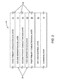
- Figure 2 shows details of a first multiple sub-layer metallization layer illustrated in Figure 1 according to one embodiment of the first multiple sub-layer metallization layer.
- Figure 3 shows details of the first multiple sub-layer metallization layer illustrated in Figure 1 according to an alternate embodiment of the first multiple sub-layer metallization layer.
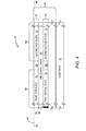
- Figure 4 shows details of the semiconductor die according to an alternate embodiment of the semiconductor die.
- Figure 5 shows details of the semiconductor die according to an additional embodiment of the semiconductor die.
- Figure 6 shows details of the semiconductor die according to another embodiment of the semiconductor die.
- Figure 7 shows details of the semiconductor die according to a further embodiment of the semiconductor die.
- Figure 8 illustrates a process for providing the semiconductor die illustrated in Figure 1 according to one embodiment of the process.
- Figure 9 illustrates a process for providing the semiconductor die illustrated in Figure 1 according to an alternate embodiment of the process.
- Figure 1 shows details of a semiconductor die 10 according to one embodiment of the semiconductor die 10.
- the semiconductor die 10 includes a substrate 12 and a multi-layer structure 14, which is on the substrate 12.
- the multi-layer structure 14 includes a first multiple sub-layer metallization layer 16, which is over the substrate 12.
- the first multiple sub-layer metallization layer 16 is on the substrate 12.
- the substrate 12 includes silicon carbide.
- the multi-layer structure 14 includes at least one epitaxial layer.
- FIG 2 shows details of the first multiple sub-layer metallization layer 16 illustrated in Figure 1 according to one embodiment of the first multiple sub-layer metallization layer 16.
- the first multiple sub-layer metallization layer 16 includes an adhesion layer 18; a diffusion barrier layer 20, which is on the adhesion layer 18; a first group 22 of primary conduction sub-layers, which is over the substrate 12 ( Figure 1 ); and a first group 24 of separation sub-layers, which is over the substrate 12 ( Figure 1 ).
- the first group 22 of primary conduction sub-layers and the first group 24 of separation sub-layers are on the diffusion barrier layer 20.
- the first multiple sub-layer metallization layer 16 further includes a first primary conduction sub-layer 26, which is on the diffusion barrier layer 20; a first separation sub-layer 28, which is on the first primary conduction sub-layer 26; a second primary conduction sub-layer 30, which is on the first separation sub-layer 28; a second separation sub-layer 32, which is on the second primary conduction sub-layer 30; and a third primary conduction sub-layer 34, which is on the second separation sub-layer 32.
- the first group 22 of primary conduction sub-layers includes the first primary conduction sub-layer 26, the second primary conduction sub-layer 30, and the third primary conduction sub-layer 34.
- the first group 24 of separation sub-layers includes the first separation sub-layer 28 and the second separation sub-layer 32.
- each adjacent pair of the first group 22 of primary conduction sub-layers is separated by at least one of the first group 24 of separation sub-layers.
- the first group 24 of separation sub-layers mitigates grain growth in the first group 22 of primary conduction sub-layers.
- the first multiple sub-layer metallization layer 16 includes at least two primary conduction sub-layers 26, 30 and the first separation sub-layer 28.
- the first separation sub-layer 28 is disposed between the at least two primary conduction sub-layers 26, 30.
- the first separation sub-layer 28 is adapted to mitigate grain growth in the at least two primary conduction sub-layers 26, 30.
- each of first group 24 of separation sub-layers is disposed between each adjacent pair of the at least two primary conduction sub-layers 26, 30, and the first group 24 of separation sub-layers is adapted to mitigate grain growth in the at least two primary conduction sub-layers 26, 30.
- one of the at least two primary conduction sub-layers 26, 30 is on the substrate 12 ( Figure 1 ).
- an effective thickness of the first multiple sub-layer metallization layer 16 may be fairly large, while keeping the thickness of each of the primary conduction sub-layers 26, 30, 34 fairly small.
- grain boundaries in the primary conduction sub-layers 26, 30, 34 may be substantially frozen, which may reduce stresses that would otherwise be induced from thermal cycling of the semiconductor die 10 ( Figure 1 ).
- the grain growth in the primary conduction sub-layers 26, 30, 34 is substantially reduced, thereby preventing fatigue induced failures in the semiconductor die 10 ( Figure 1 ).
- the grain growth of conducting metal, such as gold, in each of the primary conduction sub-layers 26, 30, 34 may be large. By freezing the grain boundaries in the primary conduction sub-layers 26, 30, 34, the grain growth of the conducting metal is effectively limited. Otherwise, voids or excessive thickening of the conducting metal could occur.
- the first primary conduction sub-layer 26 includes gold. In one embodiment of the first primary conduction sub-layer 26, a concentration of gold in the first primary conduction sub-layer 26 exceeds 99 percent. In one embodiment of the second primary conduction sub-layer 30, the second primary conduction sub-layer 30 includes gold. In one embodiment of the second primary conduction sub-layer 30, a concentration of gold in the second primary conduction sub-layer 30 exceeds 99 percent. In one embodiment of the third primary conduction sub-layer 34, the third primary conduction sub-layer 34 includes gold. In one embodiment of the third primary conduction sub-layer 34, a concentration of gold in the third primary conduction sub-layer 34 exceeds 99 percent. In one embodiment of the first group 22 of primary conduction sub-layers, each of the first group 22 of primary conduction sub-layers includes gold.
- a concentration of gold in each of the first group 22 of primary conduction sub-layers exceeds 90 percent. In a second embodiment of the first group 22 of primary conduction sub-layers, a concentration of gold in each of the first group 22 of primary conduction sub-layers exceeds 90 percent. In a third embodiment of the first group 22 of primary conduction sub-layers, a concentration of gold in each of the first group 22 of primary conduction sub-layers exceeds 92 percent. In a fourth embodiment of the first group 22 of primary conduction sub-layers, a concentration of gold in each of the first group 22 of primary conduction sub-layers exceeds 94 percent.
- a concentration of gold in each of the first group 22 of primary conduction sub-layers exceeds 95 percent. In a sixth embodiment of the first group 22 of primary conduction sub-layers, a concentration of gold in each of the first group 22 of primary conduction sub-layers exceeds 96 percent. In a seventh embodiment of the first group 22 of primary conduction sub-layers, a concentration of gold in each of the first group 22 of primary conduction sub-layers exceeds 97 percent. In an eighth embodiment of the first group 22 of primary conduction sub-layers, a concentration of gold in each of the first group 22 of primary conduction sub-layers exceeds 98 percent. In a ninth embodiment of the first group 22 of primary conduction sub-layers, a concentration of gold in each of the first group 22 of primary conduction sub-layers exceeds 99 percent.
- each of the first group 22 of primary conduction sub-layers does not include copper. In one embodiment of the first group 22 of primary conduction sub-layers, each of the first group 22 of primary conduction sub-layers does not include silver. In one embodiment of the first group 22 of primary conduction sub-layers, each of the first group 22 of primary conduction sub-layers does not include aluminum.
- a thickness of each of the first group 22 of primary conduction sub-layers is less than or equal to about 50,000 Angstroms. In a second embodiment of the first group 22 of primary conduction sub-layers, the thickness of each of the first group 22 of primary conduction sub-layers is less than or equal to about 40,000 Angstroms. In a third embodiment of the first group 22 of primary conduction sub-layers, the thickness of each of the first group 22 of primary conduction sub-layers is less than or equal to about 30,000 Angstroms.
- the thickness of each of the first group 22 of primary conduction sub-layers is less than or equal to about 20,000 Angstroms. In a fifth embodiment of the first group 22 of primary conduction sub-layers, the thickness of each of the first group 22 of primary conduction sub-layers is less than or equal to about 10,000 Angstroms. In a sixth embodiment of the first group 22 of primary conduction sub-layers, the thickness of each of the first group 22 of primary conduction sub-layers is less than or equal to about 5,000 Angstroms. In an exemplary embodiment of the first group 22 of primary conduction sub-layers, the thickness of each of the first group 22 of primary conduction sub-layers is equal to about 10,000 Angstroms.
- the adhesion layer 18 includes titanium. In a second embodiment of the adhesion layer 18, the adhesion layer 18 includes nickel. In one embodiment of the adhesion layer 18, a thickness of the adhesion layer 18 is equal to about 500 Angstroms. In a first embodiment of the diffusion barrier layer 20, the diffusion barrier layer 20 includes titanium. In a second embodiment of the diffusion barrier layer 20, the diffusion barrier layer 20 includes nickel. In a third embodiment of the diffusion barrier layer 20, the diffusion barrier layer 20 includes platinum. In one embodiment of the diffusion barrier layer 20, a thickness of the diffusion barrier layer 20 is equal to about 100 Angstroms. In an alternate embodiment of the first multiple sub-layer metallization layer 16, the adhesion layer 18 is omitted. In another embodiment of the first multiple sub-layer metallization layer 16, the diffusion barrier layer 20 is omitted. In a further embodiment of the first multiple sub-layer metallization layer 16, both the adhesion layer 18 and the diffusion barrier layer 20 are omitted.
- the first separation sub-layer 28 includes titanium. In a second embodiment of the first separation sub-layer 28, the first separation sub-layer 28 includes nickel. In a third embodiment of the first separation sub-layer 28, the first separation sub-layer 28 includes platinum. In a first embodiment of the second separation sub-layer 32, the second separation sub-layer 32 includes titanium. In a second embodiment of the second separation sub-layer 32, the second separation sub-layer 32 includes nickel. In a third embodiment of the second separation sub-layer 32, the second separation sub-layer 32 includes platinum. In a first embodiment of the first group 24 of separation sub-layers, at least one of the first group 24 of separation sub-layers includes titanium.
- At least one of the first group 24 of separation sub-layers includes nickel. In a third embodiment of the first group 24 of separation sub-layers, at least one of the first group 24 of separation sub-layers includes platinum.
- a thickness of the first separation sub-layer 28 is equal to about 100 Angstroms. In an exemplary embodiment of the second separation sub-layer 32, a thickness of the second separation sub-layer 32 is equal to about 100 Angstroms. In an exemplary embodiment of the first group 24 of separation sub-layers, a thickness of each of the first group 24 of separation sub-layers is equal to about 100 Angstroms.
- the thickness of each of the first group 22 of primary conduction sub-layers is equal to at least two times the thickness of each of the first group 24 of separation sub-layers. In a second embodiment of the first group 22 of primary conduction sub-layers and the first group 24 of separation sub-layers, the thickness of each of the first group 22 of primary conduction sub-layers is equal to at least five times the thickness of each of the first group 24 of separation sub-layers.
- the thickness of each of the first group 22 of primary conduction sub-layers is equal to at least ten times the thickness of each of the first group 24 of separation sub-layers. In a fourth embodiment of the first group 22 of primary conduction sub-layers and the first group 24 of separation sub-layers, the thickness of each of the first group 22 of primary conduction sub-layers is equal to at least twenty times the thickness of each of the first group 24 of separation sub-layers.
- the thickness of each of the first group 22 of primary conduction sub-layers is equal to at least fifty times the thickness of each of the first group 24 of separation sub-layers.
- the thickness of each of the first group 22 of primary conduction sub-layers is equal to at least 100 times the thickness of each of the first group 24 of separation sub-layers.
- the thickness of each of the first group 22 of primary conduction sub-layers is equal to at least 200 times the thickness of each of the first group 24 of separation sub-layers.
- the thickness of each of the first group 22 of primary conduction sub-layers is equal to at least 500 times the thickness of each of the first group 24 of separation sub-layers. In a ninth embodiment of the first group 22 of primary conduction sub-layers and the first group 24 of separation sub-layers, the thickness of each of the first group 22 of primary conduction sub-layers is equal to about 1000 times the thickness of each of the first group 24 of separation sub-layers.
- Figure 3 shows details of the first multiple sub-layer metallization layer 16 illustrated in Figure 1 according to an alternate embodiment of the first multiple sub-layer metallization layer 16.
- the first multiple sub-layer metallization layer 16 illustrated in Figure 3 is similar to the first multiple sub-layer metallization layer 16 illustrated in Figure 2 , except in the first multiple sub-layer metallization layer 16 illustrated in Figure 3 , the third primary conduction sub-layer 34 is omitted and the first group 24 of separation sub-layers further includes a third separation sub-layer 36.
- the second separation sub-layer 32 is on the first separation sub-layer 28
- the third separation sub-layer 36 is on the second separation sub-layer 32
- the second primary conduction sub-layer 30 is on the third separation sub-layer 36.
- the third separation sub-layer 36 includes titanium. In a second embodiment of the third separation sub-layer 36, the third separation sub-layer 36 includes nickel. In a third embodiment of the third separation sub-layer 36, the third separation sub-layer 36 includes platinum.
- the thickness of the first primary conduction sub-layer 26 is equal to about 25,000 Angstroms. In an exemplary embodiment of the second primary conduction sub-layer 30, the thickness of the second primary conduction sub-layer 30 is equal to about 5,000 Angstroms. In an exemplary embodiment of the first separation sub-layer 28, the thickness of the first separation sub-layer 28 is equal to about 100 Angstroms. In an exemplary embodiment of the second separation sub-layer 32, the thickness of the second separation sub-layer 32 is equal to about 2,500 Angstroms. In an exemplary embodiment of the third separation sub-layer 36, a thickness of the third separation sub-layer 36 is equal to about 100 Angstroms.
- Figure 4 shows details of the semiconductor die 10 according to an alternate embodiment of the semiconductor die 10.
- the semiconductor die 10 illustrated in Figure 4 includes a first capacitive element 38 and a second capacitive element 40.
- the semiconductor die 10 includes the substrate 12 and the multi-layer structure 14, which is on the substrate 12.
- the multi-layer structure 14 includes the first multiple sub-layer metallization layer 16, a dielectric layer 42, and a second multiple sub-layer metallization layer 44.
- the second multiple sub-layer metallization layer 44 is over the substrate 12, the dielectric layer 42 is on the second multiple sub-layer metallization layer 44, and the first multiple sub-layer metallization layer 16 is on the dielectric layer 42.
- the second multiple sub-layer metallization layer 44 includes a second group 46 of primary conduction sub-layers and a second group 48 of separation sub-layers. As such, the second group 46 of primary conduction sub-layers is over the substrate 12 and the second group 48 of separation sub-layers is over the substrate 12.
- the second multiple sub-layer metallization layer 44 may be similar in construction to the first multiple sub-layer metallization layer 16. In this regard, each adjacent pair of the second group 46 of primary conduction sub-layers is separated by at least one of the second group 48 of separation sub-layers. As a result, the second group 48 of separation sub-layers mitigates grain growth in the second group 46 of primary conduction sub-layers.
- a first top plate 50 of the first capacitive element 38 includes a first portion of the first multiple sub-layer metallization layer 16.
- a first bottom plate 52 of the first capacitive element 38 includes a first portion of the second multiple sub-layer metallization layer 44.
- a first portion of the dielectric layer 42 is on the first bottom plate 52 and the first top plate 50 is on the first portion of the dielectric layer 42.
- the first capacitive element 38 includes the first top plate 50, the first bottom plate 52, and the first portion of the dielectric layer 42.
- a second top plate 54 of the second capacitive element 40 includes a second portion of the first multiple sub-layer metallization layer 16.
- a second bottom plate 56 of the second capacitive element 40 includes a second portion of the second multiple sub-layer metallization layer 44.
- a second portion of the dielectric layer 42 is on the second bottom plate 56 and the second top plate 54 is on the second portion of the dielectric layer 42.
- the second capacitive element 40 includes the second top plate 54, the second bottom plate 56, and the second portion of the dielectric layer 42.
- the first multiple sub-layer metallization layer 16 provides a first electrical interconnect 58 between the first top plate 50 and the second top plate 54.
- the second multiple sub-layer metallization layer 44 provides a second electrical interconnect 60 between the first bottom plate 52 and the second bottom plate 56. Therefore, the first capacitive element 38 and the second capacitive element 40 are coupled in parallel. As such, the first multiple sub-layer metallization layer 16 provides an electrical interconnect between the first capacitive element 38 and the second capacitive element 40.
- the second multiple sub-layer metallization layer 44 provides an electrical interconnect between the first capacitive element 38 and the second capacitive element 40.
- the semiconductor die 10 includes at least two electrical devices.
- the first multiple sub-layer metallization layer 16 provides at least one electrical interconnect between the two devices.
- the second multiple sub-layer metallization layer 44 provides at least one electrical interconnect between the two devices.
- a top-view cross-section 62 of the semiconductor die 10 traverses the first multiple sub-layer metallization layer 16.
- Figure 5 shows details of the semiconductor die 10 according to an additional embodiment of the semiconductor die 10. As such, Figure 5 illustrates the top-view cross-section 62 ( Figure 4 ) of the semiconductor die 10.
- the semiconductor die 10 includes the first top plate 50 and the second top plate 54.
- the first electrical interconnect 58 couples the first top plate 50 to the second top plate 54. Portions of the dielectric layer 42 are visible where the first multiple sub-layer metallization layer 16 is not present.
- FIG. 6 shows details of the semiconductor die 10 according to another embodiment of the semiconductor die 10.
- the semiconductor die 10 includes the substrate 12 and the multi-layer structure 14, which is on the substrate 12.
- the multi-layer structure 14 includes a metallization layer 64, a first layer 66, a second layer 68, the first multiple sub-layer metallization layer 16, and the second multiple sub-layer metallization layer 44.
- the first layer 66 is on a portion of the metallization layer 64.
- the second layer 68 is over the first layer 66.
- the second layer 68 is on the first layer 66.
- a first portion of the first multiple sub-layer metallization layer 16 is on the second layer 68.
- a first portion of the second multiple sub-layer metallization layer 44 is on the first multiple sub-layer metallization layer 16 and a second portion of the second multiple sub-layer metallization layer 44 is on the second layer 68.
- the first layer 66 is an epitaxial layer.
- the second layer 68 is an epitaxial layer.
- a Via 70 traverses between the first layer 66 and the second layer 68, such that a portion of the metallization layer 64 traverses between the first layer 66 and the second layer 68.
- a second portion of the first multiple sub-layer metallization layer 16 is over the Via 70, such that the metallization layer 64 is electrically connected to the first multiple sub-layer metallization layer 16.
- a Via membrane 72 which is over the Via 70, includes the second portion of the first multiple sub-layer metallization layer 16.
- a third portion of the second multiple sub-layer metallization layer 44 is over the Via 70, such that the Via membrane 72 includes the third portion of the second multiple sub-layer metallization layer 44.
- At least one additional layer (not shown) is disposed between the first layer 66 and the second layer 68, such that the multi-layer structure 14 includes a group of layers 66, 68 and the Via 70 traverses between two of the group of layers 66, 68.
- the second multiple sub-layer metallization layer 44 is omitted.
- FIG. 7 shows details of the semiconductor die 10 according to a further embodiment of the semiconductor die 10.
- the semiconductor die 10 includes the substrate 12 and the multi-layer structure 14, which is on the substrate 12.
- the multi-layer structure 14 includes a channel layer 74, a gate oxide 76, a gate 78, and the first multiple sub-layer metallization layer 16.
- the semiconductor die 10 further includes a field effect transistor (FET) element 80, which includes the gate 78, a source 82, and a drain 84.
- FET field effect transistor
- the channel layer 74 is over the substrate 12, the gate oxide 76 is on the channel layer 74, and the gate 78 is on the gate oxide 76.
- the channel layer 74 includes the source 82 and the drain 84, such that the gate 78 is between the source 82 and the drain 84.
- a first portion of the first multiple sub-layer metallization layer 16 provides a gate ohmic connection 86, which is on the gate 78.
- a second portion of the first multiple sub-layer metallization layer 16 provides a source ohmic connection 88, which is on the source 82.
- a third portion of the first multiple sub-layer metallization layer 16 provides a drain ohmic connection 90, which is on the drain 84.
- the first multiple sub-layer metallization layer 16 provides at least one ohmic connection to at least one of the source 82, the drain 84, and the gate 78.
- the semiconductor die 10 includes at least one semiconductor device (not shown), which may include at least one diode, at least one transistor, at least one photocell, at least one solar cell, at least one thyristor, at least one logic gate, at least one logic device, at least one microprocessor, at least one charge-coupled device, at least one random access memory, at least one read only memory, at least one Hall effect device, the like, or any combination thereof.
- semiconductor device not shown
- the semiconductor device may include at least one diode, at least one transistor, at least one photocell, at least one solar cell, at least one thyristor, at least one logic gate, at least one logic device, at least one microprocessor, at least one charge-coupled device, at least one random access memory, at least one read only memory, at least one Hall effect device, the like, or any combination thereof.
- the first multiple sub-layer metallization layer 16 provides at least one ohmic connection to at least one of the at least one diode, the at least one transistor, the at least one photocell, the at least one solar cell, the at least one thyristor, the at least one logic gate, the at least one logic device, the at least one microprocessor, the at least one charge-coupled device, the at least one random access memory, the at least one read only memory, the at least one Hall effect device, the like, or any combination thereof.
- the at least one diode may include at least one rectifier diode, at least one small signal diode, at least one Gunn diode, at least one light emitting diode, at least one PIN diode, at least one Schottky diode, at least one tunnel diode, at least one zener diode, the like, or any combination thereof.
- the at least one transistor may include at least one bipolar junction transistor (BJT), at least one insulated gate bipolar transistor, at least one FET, at least one metal oxide semiconductor FET (MOSFET), at least one metal-semiconductor FET (MESFET), at least one junction FET (JFET), at least one unijunction transistor, at least one high electron mobility transistor (HEMT), the like, or any combination thereof.
- the at least one thyristor may include at least one silicon controlled rectifier (SCR), at least one diode for AC (DIAC), at least one triode for AC (TRIAC), the like, or any combination thereof.
- Figure 8 illustrates a process for providing the semiconductor die 10 illustrated in Figure 1 according to one embodiment of the process.
- the process begins by providing a semiconductor die 10 having a substrate 12 (Step 100).
- the process continues by forming a first of the first group 22 of primary conduction sub-layers over the substrate 12 (Step 102).
- the process proceeds by forming at least a first of the first group 24 of separation sub-layers on the first of the first group 22 of primary conduction sub-layers (Step 104).
- the process concludes by forming a last of the first group 22 of primary conduction sub-layers over the first of the first group 24 of separation sub-layers, such that the first group 24 of separation sub-layers is adapted to mitigate grain growth in the first group 22 of primary conduction sub-layers (Step 106).
- Figure 9 illustrates a process for providing the semiconductor die 10 illustrated in Figure 1 according to an alternate embodiment of the process.
- the process begins by providing a semiconductor die 10 having a substrate 12 (Step 200).
- the process continues by forming a first of the first group 22 of primary conduction sub-layers over the substrate 12 using evaporation (Step 202).
- the process proceeds by forming at least a first of the first group 24 of separation sub-layers on the first of the first group 22 of primary conduction sub-layers using evaporation (Step 204).
- the process concludes by forming a last of the first group 22 of primary conduction sub-layers over the first of the first group 24 of separation sub-layers using evaporation, such that the first group 24 of separation sub-layers is adapted to mitigate grain growth in the first group 22 of primary conduction sub-layers (Step 206).
Landscapes
- Chemical & Material Sciences (AREA)
- Engineering & Computer Science (AREA)
- Chemical Kinetics & Catalysis (AREA)
- Materials Engineering (AREA)
- Mechanical Engineering (AREA)
- Metallurgy (AREA)
- Organic Chemistry (AREA)
- Electrodes Of Semiconductors (AREA)
- Semiconductor Integrated Circuits (AREA)
- Internal Circuitry In Semiconductor Integrated Circuit Devices (AREA)
- Power Engineering (AREA)
- Recrystallisation Techniques (AREA)
Abstract
Description
- Embodiments of the present disclosure relate to metallization layers, which are used in the fabrication of integrated circuits.
- Over the life of an integrated circuit (IC), the IC may be subjected to many thermal cycles, which may induce certain types of stresses. Such stresses may lead to fatigue induced failures in certain structures in the IC. As a result, the reliability of the IC may be significantly reduced. Therefore, to maximize the reliability of an IC, there is a need to mitigate the effects of stresses that are caused by thermal cycles.
- Embodiments of the present disclosure relate to a semiconductor die, which includes a substrate, a group of primary conduction sub-layers, which is over the substrate, and a group of separation sub-layers. Each adjacent pair of the group of primary conduction sub-layers is separated by at least one of the group of separation sub-layers. As a result, the group of separation sub-layers mitigates grain growth in the group of primary conduction sub-layers.
- In one embodiment of the present disclosure, the group of primary conduction sub-layers and the group of separation sub-layers provide a multiple sub-layer metallization layer over the substrate. By using multiple primary conduction sub-layers, an effective thickness of the multiple sub-layer metallization layer may be fairly large, while keeping the thickness of each primary conduction sub-layer fairly small. By layering the primary conduction sub-layers, grain boundaries in the primary conduction sub-layers may be substantially frozen, which may reduce stresses that would otherwise be induced from thermal cycling of the semiconductor die. As a result, grain growth in the primary conduction sub-layers is substantially reduced, thereby preventing fatigue induced failures in the semiconductor die. In this regard, the grain growth of conducting metal, such as gold, in each primary conduction sub-layer may be large. By freezing the grain boundaries in the primary conduction sub-layers, the grain growth of the conducting metal is effectively limited. Otherwise, voids or excessive thickening of the conducting metal could occur.
- In one embodiment of the present disclosure, the semiconductor die includes the substrate, a first multiple sub-layer metallization layer, which is over the substrate, and a second multiple sub-layer metallization layer, which is over the first multiple sub-layer metallization layer. The first multiple sub-layer metallization layer includes a first group of primary conduction sub-layers and a first group of separation sub-layers. Each adjacent pair of the first group of primary conduction sub-layers is separated by at least one of the first group of separation sub-layers. As a result, the first group of separation sub-layers mitigates grain growth in the first group of primary conduction sub-layers. The second multiple sub-layer metallization layer includes a second group of primary conduction sub-layers and a second group of separation sub-layers. Each adjacent pair of the second group of primary conduction sub-layers is separated by at least one of the second group of separation sub-layers. As a result, the second group of separation sub-layers mitigates grain growth in the second group of primary conduction sub-layers.
- Those skilled in the art will appreciate the scope of the disclosure and realize additional aspects thereof after reading the following detailed description in association with the accompanying drawings.
- The accompanying drawings incorporated in and forming a part of this specification illustrate several aspects of the disclosure, and together with the description serve to explain the principles of the disclosure.
-
Figure 1 shows details of a semiconductor die according to one embodiment of the semiconductor die. -
Figure 2 shows details of a first multiple sub-layer metallization layer illustrated inFigure 1 according to one embodiment of the first multiple sub-layer metallization layer. -
Figure 3 shows details of the first multiple sub-layer metallization layer illustrated inFigure 1 according to an alternate embodiment of the first multiple sub-layer metallization layer. -
Figure 4 shows details of the semiconductor die according to an alternate embodiment of the semiconductor die. -
Figure 5 shows details of the semiconductor die according to an additional embodiment of the semiconductor die. -
Figure 6 shows details of the semiconductor die according to another embodiment of the semiconductor die. -
Figure 7 shows details of the semiconductor die according to a further embodiment of the semiconductor die. -
Figure 8 illustrates a process for providing the semiconductor die illustrated inFigure 1 according to one embodiment of the process. -
Figure 9 illustrates a process for providing the semiconductor die illustrated inFigure 1 according to an alternate embodiment of the process. - The embodiments set forth below represent the necessary information to enable those skilled in the art to practice the disclosure and illustrate the best mode of practicing the disclosure. Upon reading the following description in light of the accompanying drawings, those skilled in the art will understand the concepts of the disclosure and will recognize applications of these concepts not particularly addressed herein. It should be understood that these concepts and applications fall within the scope of the disclosure and the accompanying claims.
- It will be understood that when an element such as a layer, region, or substrate is referred to as being "over," "on," "in," or extending "onto" another element, it can be directly over, directly on, directly in, or extend directly onto the other element or intervening elements may also be present. In contrast, when an element is referred to as being "directly over," "directly on," "directly in," or extending "directly onto" another element, there are no intervening elements present. It will also be understood that when an element is referred to as being "connected" or "coupled" to another element, it can be directly connected or coupled to the other element or intervening elements may be present. In contrast, when an element is referred to as being "directly connected" or "directly coupled" to another element, there are no intervening elements present.
- Relative terms such as "below" or "above" or "upper" or "lower" or "horizontal" or "vertical" may be used herein to describe a relationship of one element, layer, or region to another element, layer, or region as illustrated in the Figures. It will be understood that these terms and those discussed above are intended to encompass different orientations of the device in addition to the orientation depicted in the Figures.
-
Figure 1 shows details of a semiconductor die 10 according to one embodiment of the semiconductor die 10. The semiconductor die 10 includes asubstrate 12 and amulti-layer structure 14, which is on thesubstrate 12. Themulti-layer structure 14 includes a first multiplesub-layer metallization layer 16, which is over thesubstrate 12. In one embodiment of the semiconductor die 10, the first multiplesub-layer metallization layer 16 is on thesubstrate 12. In one embodiment of thesubstrate 12, thesubstrate 12 includes silicon carbide. In one embodiment of themulti-layer structure 14, themulti-layer structure 14 includes at least one epitaxial layer. -
Figure 2 shows details of the first multiplesub-layer metallization layer 16 illustrated inFigure 1 according to one embodiment of the first multiplesub-layer metallization layer 16. The first multiplesub-layer metallization layer 16 includes anadhesion layer 18; adiffusion barrier layer 20, which is on theadhesion layer 18; afirst group 22 of primary conduction sub-layers, which is over the substrate 12 (Figure 1 ); and afirst group 24 of separation sub-layers, which is over the substrate 12 (Figure 1 ). As such, thefirst group 22 of primary conduction sub-layers and thefirst group 24 of separation sub-layers are on thediffusion barrier layer 20. The first multiplesub-layer metallization layer 16 further includes a firstprimary conduction sub-layer 26, which is on thediffusion barrier layer 20; afirst separation sub-layer 28, which is on the firstprimary conduction sub-layer 26; a secondprimary conduction sub-layer 30, which is on thefirst separation sub-layer 28; asecond separation sub-layer 32, which is on the secondprimary conduction sub-layer 30; and a thirdprimary conduction sub-layer 34, which is on thesecond separation sub-layer 32. As such, thefirst group 22 of primary conduction sub-layers includes the firstprimary conduction sub-layer 26, the secondprimary conduction sub-layer 30, and the thirdprimary conduction sub-layer 34. Thefirst group 24 of separation sub-layers includes thefirst separation sub-layer 28 and thesecond separation sub-layer 32. - In general, each adjacent pair of the
first group 22 of primary conduction sub-layers is separated by at least one of thefirst group 24 of separation sub-layers. As a result, thefirst group 24 of separation sub-layers mitigates grain growth in thefirst group 22 of primary conduction sub-layers. In one embodiment of the first multiplesub-layer metallization layer 16, the first multiplesub-layer metallization layer 16 includes at least twoprimary conduction sub-layers first separation sub-layer 28. Thefirst separation sub-layer 28 is disposed between the at least twoprimary conduction sub-layers first separation sub-layer 28 is adapted to mitigate grain growth in the at least twoprimary conduction sub-layers sub-layer metallization layer 16, each offirst group 24 of separation sub-layers is disposed between each adjacent pair of the at least twoprimary conduction sub-layers first group 24 of separation sub-layers is adapted to mitigate grain growth in the at least twoprimary conduction sub-layers sub-layer metallization layer 16, one of the at least two primary conduction sub-layers 26, 30 is on the substrate 12 (Figure 1 ). - By using multiple primary conduction sub-layers 26, 30, 34, an effective thickness of the first multiple
sub-layer metallization layer 16 may be fairly large, while keeping the thickness of each of the primary conduction sub-layers 26, 30, 34 fairly small. By layering the primary conduction sub-layers 26, 30, 34, grain boundaries in the primary conduction sub-layers 26, 30, 34 may be substantially frozen, which may reduce stresses that would otherwise be induced from thermal cycling of the semiconductor die 10 (Figure 1 ). - As a result, grain growth in the primary conduction sub-layers 26, 30, 34 is substantially reduced, thereby preventing fatigue induced failures in the semiconductor die 10 (
Figure 1 ). In this regard, the grain growth of conducting metal, such as gold, in each of the primary conduction sub-layers 26, 30, 34 may be large. By freezing the grain boundaries in the primary conduction sub-layers 26, 30, 34, the grain growth of the conducting metal is effectively limited. Otherwise, voids or excessive thickening of the conducting metal could occur. - In one embodiment of the first
primary conduction sub-layer 26, the firstprimary conduction sub-layer 26 includes gold. In one embodiment of the firstprimary conduction sub-layer 26, a concentration of gold in the firstprimary conduction sub-layer 26 exceeds 99 percent. In one embodiment of the secondprimary conduction sub-layer 30, the secondprimary conduction sub-layer 30 includes gold. In one embodiment of the secondprimary conduction sub-layer 30, a concentration of gold in the secondprimary conduction sub-layer 30 exceeds 99 percent. In one embodiment of the thirdprimary conduction sub-layer 34, the thirdprimary conduction sub-layer 34 includes gold. In one embodiment of the thirdprimary conduction sub-layer 34, a concentration of gold in the thirdprimary conduction sub-layer 34 exceeds 99 percent. In one embodiment of thefirst group 22 of primary conduction sub-layers, each of thefirst group 22 of primary conduction sub-layers includes gold. - In a first embodiment of the
first group 22 of primary conduction sub-layers, a concentration of gold in each of thefirst group 22 of primary conduction sub-layers exceeds 90 percent. In a second embodiment of thefirst group 22 of primary conduction sub-layers, a concentration of gold in each of thefirst group 22 of primary conduction sub-layers exceeds 90 percent. In a third embodiment of thefirst group 22 of primary conduction sub-layers, a concentration of gold in each of thefirst group 22 of primary conduction sub-layers exceeds 92 percent. In a fourth embodiment of thefirst group 22 of primary conduction sub-layers, a concentration of gold in each of thefirst group 22 of primary conduction sub-layers exceeds 94 percent. In a fifth embodiment of thefirst group 22 of primary conduction sub-layers, a concentration of gold in each of thefirst group 22 of primary conduction sub-layers exceeds 95 percent. In a sixth embodiment of thefirst group 22 of primary conduction sub-layers, a concentration of gold in each of thefirst group 22 of primary conduction sub-layers exceeds 96 percent. In a seventh embodiment of thefirst group 22 of primary conduction sub-layers, a concentration of gold in each of thefirst group 22 of primary conduction sub-layers exceeds 97 percent. In an eighth embodiment of thefirst group 22 of primary conduction sub-layers, a concentration of gold in each of thefirst group 22 of primary conduction sub-layers exceeds 98 percent. In a ninth embodiment of thefirst group 22 of primary conduction sub-layers, a concentration of gold in each of thefirst group 22 of primary conduction sub-layers exceeds 99 percent. - In one embodiment of the
first group 22 of primary conduction sub-layers, each of thefirst group 22 of primary conduction sub-layers does not include copper. In one embodiment of thefirst group 22 of primary conduction sub-layers, each of thefirst group 22 of primary conduction sub-layers does not include silver. In one embodiment of thefirst group 22 of primary conduction sub-layers, each of thefirst group 22 of primary conduction sub-layers does not include aluminum. - In a first embodiment of the
first group 22 of primary conduction sub-layers, a thickness of each of thefirst group 22 of primary conduction sub-layers is less than or equal to about 50,000 Angstroms. In a second embodiment of thefirst group 22 of primary conduction sub-layers, the thickness of each of thefirst group 22 of primary conduction sub-layers is less than or equal to about 40,000 Angstroms. In a third embodiment of thefirst group 22 of primary conduction sub-layers, the thickness of each of thefirst group 22 of primary conduction sub-layers is less than or equal to about 30,000 Angstroms. In a fourth embodiment of thefirst group 22 of primary conduction sub-layers, the thickness of each of thefirst group 22 of primary conduction sub-layers is less than or equal to about 20,000 Angstroms. In a fifth embodiment of thefirst group 22 of primary conduction sub-layers, the thickness of each of thefirst group 22 of primary conduction sub-layers is less than or equal to about 10,000 Angstroms. In a sixth embodiment of thefirst group 22 of primary conduction sub-layers, the thickness of each of thefirst group 22 of primary conduction sub-layers is less than or equal to about 5,000 Angstroms. In an exemplary embodiment of thefirst group 22 of primary conduction sub-layers, the thickness of each of thefirst group 22 of primary conduction sub-layers is equal to about 10,000 Angstroms. - In a first embodiment of the
adhesion layer 18, theadhesion layer 18 includes titanium. In a second embodiment of theadhesion layer 18, theadhesion layer 18 includes nickel. In one embodiment of theadhesion layer 18, a thickness of theadhesion layer 18 is equal to about 500 Angstroms. In a first embodiment of thediffusion barrier layer 20, thediffusion barrier layer 20 includes titanium. In a second embodiment of thediffusion barrier layer 20, thediffusion barrier layer 20 includes nickel. In a third embodiment of thediffusion barrier layer 20, thediffusion barrier layer 20 includes platinum. In one embodiment of thediffusion barrier layer 20, a thickness of thediffusion barrier layer 20 is equal to about 100 Angstroms. In an alternate embodiment of the first multiplesub-layer metallization layer 16, theadhesion layer 18 is omitted. In another embodiment of the first multiplesub-layer metallization layer 16, thediffusion barrier layer 20 is omitted. In a further embodiment of the first multiplesub-layer metallization layer 16, both theadhesion layer 18 and thediffusion barrier layer 20 are omitted. - In a first embodiment of the
first separation sub-layer 28, thefirst separation sub-layer 28 includes titanium. In a second embodiment of thefirst separation sub-layer 28, thefirst separation sub-layer 28 includes nickel. In a third embodiment of thefirst separation sub-layer 28, thefirst separation sub-layer 28 includes platinum. In a first embodiment of thesecond separation sub-layer 32, thesecond separation sub-layer 32 includes titanium. In a second embodiment of thesecond separation sub-layer 32, thesecond separation sub-layer 32 includes nickel. In a third embodiment of thesecond separation sub-layer 32, thesecond separation sub-layer 32 includes platinum. In a first embodiment of thefirst group 24 of separation sub-layers, at least one of thefirst group 24 of separation sub-layers includes titanium. In a second embodiment of thefirst group 24 of separation sub-layers, at least one of thefirst group 24 of separation sub-layers includes nickel. In a third embodiment of thefirst group 24 of separation sub-layers, at least one of thefirst group 24 of separation sub-layers includes platinum. - In an exemplary embodiment of the
first separation sub-layer 28, a thickness of thefirst separation sub-layer 28 is equal to about 100 Angstroms. In an exemplary embodiment of thesecond separation sub-layer 32, a thickness of thesecond separation sub-layer 32 is equal to about 100 Angstroms. In an exemplary embodiment of thefirst group 24 of separation sub-layers, a thickness of each of thefirst group 24 of separation sub-layers is equal to about 100 Angstroms. - In a first embodiment of the
first group 22 of primary conduction sub-layers and thefirst group 24 of separation sub-layers, the thickness of each of thefirst group 22 of primary conduction sub-layers is equal to at least two times the thickness of each of thefirst group 24 of separation sub-layers. In a second embodiment of thefirst group 22 of primary conduction sub-layers and thefirst group 24 of separation sub-layers, the thickness of each of thefirst group 22 of primary conduction sub-layers is equal to at least five times the thickness of each of thefirst group 24 of separation sub-layers. In a third embodiment of thefirst group 22 of primary conduction sub-layers and thefirst group 24 of separation sub-layers, the thickness of each of thefirst group 22 of primary conduction sub-layers is equal to at least ten times the thickness of each of thefirst group 24 of separation sub-layers. In a fourth embodiment of thefirst group 22 of primary conduction sub-layers and thefirst group 24 of separation sub-layers, the thickness of each of thefirst group 22 of primary conduction sub-layers is equal to at least twenty times the thickness of each of thefirst group 24 of separation sub-layers. In a fifth embodiment of thefirst group 22 of primary conduction sub-layers and thefirst group 24 of separation sub-layers, the thickness of each of thefirst group 22 of primary conduction sub-layers is equal to at least fifty times the thickness of each of thefirst group 24 of separation sub-layers. - In a sixth embodiment of the
first group 22 of primary conduction sub-layers and thefirst group 24 of separation sub-layers, the thickness of each of thefirst group 22 of primary conduction sub-layers is equal to at least 100 times the thickness of each of thefirst group 24 of separation sub-layers. In a seventh embodiment of thefirst group 22 of primary conduction sub-layers and thefirst group 24 of separation sub-layers, the thickness of each of thefirst group 22 of primary conduction sub-layers is equal to at least 200 times the thickness of each of thefirst group 24 of separation sub-layers. In an eighth embodiment of thefirst group 22 of primary conduction sub-layers and thefirst group 24 of separation sub-layers, the thickness of each of thefirst group 22 of primary conduction sub-layers is equal to at least 500 times the thickness of each of thefirst group 24 of separation sub-layers. In a ninth embodiment of thefirst group 22 of primary conduction sub-layers and thefirst group 24 of separation sub-layers, the thickness of each of thefirst group 22 of primary conduction sub-layers is equal to about 1000 times the thickness of each of thefirst group 24 of separation sub-layers. -
Figure 3 shows details of the first multiplesub-layer metallization layer 16 illustrated inFigure 1 according to an alternate embodiment of the first multiplesub-layer metallization layer 16. The first multiplesub-layer metallization layer 16 illustrated inFigure 3 is similar to the first multiplesub-layer metallization layer 16 illustrated inFigure 2 , except in the first multiplesub-layer metallization layer 16 illustrated inFigure 3 , the thirdprimary conduction sub-layer 34 is omitted and thefirst group 24 of separation sub-layers further includes athird separation sub-layer 36. In this regard, thesecond separation sub-layer 32 is on thefirst separation sub-layer 28, thethird separation sub-layer 36 is on thesecond separation sub-layer 32, and the secondprimary conduction sub-layer 30 is on thethird separation sub-layer 36. - In a first embodiment of the
third separation sub-layer 36, thethird separation sub-layer 36 includes titanium. In a second embodiment of thethird separation sub-layer 36, thethird separation sub-layer 36 includes nickel. In a third embodiment of thethird separation sub-layer 36, thethird separation sub-layer 36 includes platinum. - In an exemplary embodiment of the first
primary conduction sub-layer 26, the thickness of the firstprimary conduction sub-layer 26 is equal to about 25,000 Angstroms. In an exemplary embodiment of the secondprimary conduction sub-layer 30, the thickness of the secondprimary conduction sub-layer 30 is equal to about 5,000 Angstroms. In an exemplary embodiment of thefirst separation sub-layer 28, the thickness of thefirst separation sub-layer 28 is equal to about 100 Angstroms. In an exemplary embodiment of thesecond separation sub-layer 32, the thickness of thesecond separation sub-layer 32 is equal to about 2,500 Angstroms. In an exemplary embodiment of thethird separation sub-layer 36, a thickness of thethird separation sub-layer 36 is equal to about 100 Angstroms. -
Figure 4 shows details of the semiconductor die 10 according to an alternate embodiment of the semiconductor die 10. The semiconductor die 10 illustrated inFigure 4 includes afirst capacitive element 38 and asecond capacitive element 40. As such, the semiconductor die 10 includes thesubstrate 12 and themulti-layer structure 14, which is on thesubstrate 12. Themulti-layer structure 14 includes the first multiplesub-layer metallization layer 16, adielectric layer 42, and a second multiplesub-layer metallization layer 44. The second multiplesub-layer metallization layer 44 is over thesubstrate 12, thedielectric layer 42 is on the second multiplesub-layer metallization layer 44, and the first multiplesub-layer metallization layer 16 is on thedielectric layer 42. - The second multiple
sub-layer metallization layer 44 includes asecond group 46 of primary conduction sub-layers and asecond group 48 of separation sub-layers. As such, thesecond group 46 of primary conduction sub-layers is over thesubstrate 12 and thesecond group 48 of separation sub-layers is over thesubstrate 12. The second multiplesub-layer metallization layer 44 may be similar in construction to the first multiplesub-layer metallization layer 16. In this regard, each adjacent pair of thesecond group 46 of primary conduction sub-layers is separated by at least one of thesecond group 48 of separation sub-layers. As a result, thesecond group 48 of separation sub-layers mitigates grain growth in thesecond group 46 of primary conduction sub-layers. - A first
top plate 50 of thefirst capacitive element 38 includes a first portion of the first multiplesub-layer metallization layer 16. Afirst bottom plate 52 of thefirst capacitive element 38 includes a first portion of the second multiplesub-layer metallization layer 44. A first portion of thedielectric layer 42 is on thefirst bottom plate 52 and the firsttop plate 50 is on the first portion of thedielectric layer 42. As such, thefirst capacitive element 38 includes the firsttop plate 50, thefirst bottom plate 52, and the first portion of thedielectric layer 42. A secondtop plate 54 of thesecond capacitive element 40 includes a second portion of the first multiplesub-layer metallization layer 16. Asecond bottom plate 56 of thesecond capacitive element 40 includes a second portion of the second multiplesub-layer metallization layer 44. A second portion of thedielectric layer 42 is on thesecond bottom plate 56 and the secondtop plate 54 is on the second portion of thedielectric layer 42. As such, thesecond capacitive element 40 includes the secondtop plate 54, thesecond bottom plate 56, and the second portion of thedielectric layer 42. - The first multiple
sub-layer metallization layer 16 provides a firstelectrical interconnect 58 between the firsttop plate 50 and the secondtop plate 54. The second multiplesub-layer metallization layer 44 provides a secondelectrical interconnect 60 between thefirst bottom plate 52 and thesecond bottom plate 56. Therefore, thefirst capacitive element 38 and thesecond capacitive element 40 are coupled in parallel. As such, the first multiplesub-layer metallization layer 16 provides an electrical interconnect between thefirst capacitive element 38 and thesecond capacitive element 40. Similarly, the second multiplesub-layer metallization layer 44 provides an electrical interconnect between thefirst capacitive element 38 and thesecond capacitive element 40. - Since the
first capacitive element 38 and thesecond capacitive element 40 are electrical devices, in general, the semiconductor die 10 includes at least two electrical devices. The first multiplesub-layer metallization layer 16 provides at least one electrical interconnect between the two devices. Further, the second multiplesub-layer metallization layer 44 provides at least one electrical interconnect between the two devices. A top-view cross-section 62 of the semiconductor die 10 traverses the first multiplesub-layer metallization layer 16. -
Figure 5 shows details of the semiconductor die 10 according to an additional embodiment of the semiconductor die 10. As such,Figure 5 illustrates the top-view cross-section 62 (Figure 4 ) of the semiconductor die 10. The semiconductor die 10 includes the firsttop plate 50 and the secondtop plate 54. The firstelectrical interconnect 58 couples the firsttop plate 50 to the secondtop plate 54. Portions of thedielectric layer 42 are visible where the first multiplesub-layer metallization layer 16 is not present. -
Figure 6 shows details of the semiconductor die 10 according to another embodiment of the semiconductor die 10. The semiconductor die 10 includes thesubstrate 12 and themulti-layer structure 14, which is on thesubstrate 12. Themulti-layer structure 14 includes ametallization layer 64, afirst layer 66, asecond layer 68, the first multiplesub-layer metallization layer 16, and the second multiplesub-layer metallization layer 44. Thefirst layer 66 is on a portion of themetallization layer 64. Thesecond layer 68 is over thefirst layer 66. In one embodiment of the semiconductor die 10, thesecond layer 68 is on thefirst layer 66. A first portion of the first multiplesub-layer metallization layer 16 is on thesecond layer 68. A first portion of the second multiplesub-layer metallization layer 44 is on the first multiplesub-layer metallization layer 16 and a second portion of the second multiplesub-layer metallization layer 44 is on thesecond layer 68. In one embodiment of thefirst layer 66, thefirst layer 66 is an epitaxial layer. In one embodiment of thesecond layer 68, thesecond layer 68 is an epitaxial layer. - A
Via 70 traverses between thefirst layer 66 and thesecond layer 68, such that a portion of themetallization layer 64 traverses between thefirst layer 66 and thesecond layer 68. A second portion of the first multiplesub-layer metallization layer 16 is over theVia 70, such that themetallization layer 64 is electrically connected to the first multiplesub-layer metallization layer 16. In this regard, aVia membrane 72, which is over theVia 70, includes the second portion of the first multiplesub-layer metallization layer 16. Further, a third portion of the second multiplesub-layer metallization layer 44 is over theVia 70, such that theVia membrane 72 includes the third portion of the second multiplesub-layer metallization layer 44. - In an alternate embodiment of the semiconductor die 10, at least one additional layer (not shown) is disposed between the
first layer 66 and thesecond layer 68, such that themulti-layer structure 14 includes a group oflayers Via 70 traverses between two of the group oflayers sub-layer metallization layer 44 is omitted. -
Figure 7 shows details of the semiconductor die 10 according to a further embodiment of the semiconductor die 10. The semiconductor die 10 includes thesubstrate 12 and themulti-layer structure 14, which is on thesubstrate 12. Themulti-layer structure 14 includes achannel layer 74, agate oxide 76, agate 78, and the first multiplesub-layer metallization layer 16. The semiconductor die 10 further includes a field effect transistor (FET) element 80, which includes thegate 78, asource 82, and adrain 84. Thechannel layer 74 is over thesubstrate 12, thegate oxide 76 is on thechannel layer 74, and thegate 78 is on thegate oxide 76. Thechannel layer 74 includes thesource 82 and thedrain 84, such that thegate 78 is between thesource 82 and thedrain 84. A first portion of the first multiplesub-layer metallization layer 16 provides a gateohmic connection 86, which is on thegate 78. A second portion of the first multiplesub-layer metallization layer 16 provides a sourceohmic connection 88, which is on thesource 82. A third portion of the first multiplesub-layer metallization layer 16 provides a drainohmic connection 90, which is on thedrain 84. In general, the first multiplesub-layer metallization layer 16 provides at least one ohmic connection to at least one of thesource 82, thedrain 84, and thegate 78. - In alternate embodiments of the semiconductor die 10, in general, the semiconductor die 10 includes at least one semiconductor device (not shown), which may include at least one diode, at least one transistor, at least one photocell, at least one solar cell, at least one thyristor, at least one logic gate, at least one logic device, at least one microprocessor, at least one charge-coupled device, at least one random access memory, at least one read only memory, at least one Hall effect device, the like, or any combination thereof. Further, in alternate embodiments of the first multiple
sub-layer metallization layer 16, the first multiplesub-layer metallization layer 16 provides at least one ohmic connection to at least one of the at least one diode, the at least one transistor, the at least one photocell, the at least one solar cell, the at least one thyristor, the at least one logic gate, the at least one logic device, the at least one microprocessor, the at least one charge-coupled device, the at least one random access memory, the at least one read only memory, the at least one Hall effect device, the like, or any combination thereof. - The at least one diode may include at least one rectifier diode, at least one small signal diode, at least one Gunn diode, at least one light emitting diode, at least one PIN diode, at least one Schottky diode, at least one tunnel diode, at least one zener diode, the like, or any combination thereof. The at least one transistor may include at least one bipolar junction transistor (BJT), at least one insulated gate bipolar transistor, at least one FET, at least one metal oxide semiconductor FET (MOSFET), at least one metal-semiconductor FET (MESFET), at least one junction FET (JFET), at least one unijunction transistor, at least one high electron mobility transistor (HEMT), the like, or any combination thereof. The at least one thyristor may include at least one silicon controlled rectifier (SCR), at least one diode for AC (DIAC), at least one triode for AC (TRIAC), the like, or any combination thereof.
-
Figure 8 illustrates a process for providing the semiconductor die 10 illustrated inFigure 1 according to one embodiment of the process. The process begins by providing asemiconductor die 10 having a substrate 12 (Step 100). The process continues by forming a first of thefirst group 22 of primary conduction sub-layers over the substrate 12 (Step 102). The process proceeds by forming at least a first of thefirst group 24 of separation sub-layers on the first of thefirst group 22 of primary conduction sub-layers (Step 104). The process concludes by forming a last of thefirst group 22 of primary conduction sub-layers over the first of thefirst group 24 of separation sub-layers, such that thefirst group 24 of separation sub-layers is adapted to mitigate grain growth in thefirst group 22 of primary conduction sub-layers (Step 106). -
Figure 9 illustrates a process for providing the semiconductor die 10 illustrated inFigure 1 according to an alternate embodiment of the process. The process begins by providing asemiconductor die 10 having a substrate 12 (Step 200). The process continues by forming a first of thefirst group 22 of primary conduction sub-layers over thesubstrate 12 using evaporation (Step 202). The process proceeds by forming at least a first of thefirst group 24 of separation sub-layers on the first of thefirst group 22 of primary conduction sub-layers using evaporation (Step 204). The process concludes by forming a last of thefirst group 22 of primary conduction sub-layers over the first of thefirst group 24 of separation sub-layers using evaporation, such that thefirst group 24 of separation sub-layers is adapted to mitigate grain growth in thefirst group 22 of primary conduction sub-layers (Step 206). - None of the embodiments of the present disclosure are intended to limit the scope of any other embodiment of the present disclosure. Any or all of any embodiment of the present disclosure may be combined with any or all of any other embodiment of the present disclosure to create new embodiments of the present disclosure.
- Those skilled in the art will recognize improvements and modifications to the embodiments of the present disclosure. All such improvements and modifications are considered within the scope of the concepts disclosed herein and the claims that follow.
Claims (24)
- A semiconductor die comprising:at least two primary conduction sub-layers; anda first separation sub-layer, wherein:the first separation sub-layer is disposed between the at least two primary conduction sub-layers; andthe first separation sub-layer is adapted to mitigate grain growth in the at least two primary conduction sub-layers.
- The semiconductor die of claim 1 further comprising a first plurality of separation sub-layers, which comprises the first separation sub-layer, wherein at least a corresponding one of the first plurality of separation sub-layers is disposed between each adjacent pair of the at least two primary conduction sub-layers, and the first plurality of separation sub-layers is adapted to mitigate grain growth in the at least two primary conduction sub-layers.
- The semiconductor die of claim 2, wherein each of the first plurality of separation sub-layers is disposed between each adjacent pair of the at least two primary conduction sub-layers.
- The semiconductor die of any of claims 1-3 further comprising a substrate, wherein one of the at least two primary conduction sub-layers is on the substrate.
- The semiconductor die of any preceding claim wherein each of the first plurality of primary conduction sub-layers comprises gold.
- The semiconductor die of claim 5 wherein a concentration of gold in each of the first plurality of primary conduction sub-layers exceeds 99 percent.
- The semiconductor die of any of claims 1 to 6 wherein each of the first plurality of primary conduction sub-layers does not comprise copper, silver or aluminum.
- The semiconductor die of any preceding claim wherein the first separation sub-layer comprises a metal selected from nickel, platinum and titanium.
- The semiconductor die of any preceding claim wherein a thickness of each of the first plurality of primary conduction sub-layers is equal to at least ten times, and preferably twenty times, a thickness of the or each separation sub-layer(s).
- The semiconductor die of any preceding claim wherein the first plurality of primary conduction sub-layers and the or each separation sub-layer(s) provide a first multiple sub-layer metallization layer over the substrate.
- The semiconductor die of claim 10 wherein the first multiple sub-layer metallization layer further comprises:an adhesion layer; anda diffusion barrier layer on the adhesion layer, such that the first plurality of primary conduction sub-layers and the first plurality of separation sub-layers are on the diffusion barrier layer.
- The semiconductor die of claim 11 wherein the adhesion layer comprises titanium or nickel.
- The semiconductor die of claim 11 or 12 wherein the diffusion barrier layer comprises platinum or nickel.
- The semiconductor die of any of claims 10 to 13 wherein a thickness of each of the first plurality of primary conduction sub-layers is less than or equal to about 30,000 Angstroms, preferably less than or equal to about 20,000 Angstroms, and more preferably less than or equal to about 10,000 Angstroms.
- The semiconductor die of any of claims 10 to 14 further comprising a plurality of layers over the substrate, such that a Via traverses between two of the plurality of layers, and a Via membrane over the Via comprises a portion of the first multiple sub-layer metallization layer.
- The semiconductor die of any of claims 10 to 15 further comprising a second multiple sub-layer metallization layer over the substrate and comprising:a second plurality of primary conduction sub-layers; anda second plurality of separation sub-layers, wherein:at least a corresponding one of the second plurality of separation sub-layers is disposed between each adjacent pair of the second plurality of primary conduction sub-layers; andthe second plurality of separation sub-layers is adapted to mitigate grain growth in the second plurality of primary conduction sub-layers.
- The semiconductor die of claim 16 wherein a portion of the second multiple sub-layer metallization layer is on the first multiple sub-layer metallization layer.
- The semiconductor die of claim 17 further comprising a plurality of layers over the substrate, such that a Via traverses between two of the plurality of layers, and a Via membrane over the Via comprises a portion of the first multiple sub-layer metallization layer and a portion of the second multiple sub-layer metallization layer.
- The semiconductor die of any of claims 16-18 further comprising a capacitive element, such that a top plate of the capacitive element comprises a portion of the first multiple sub-layer metallization layer and a bottom plate of the capacitive element comprises a portion of the second multiple sub-layer metallization layer.
- The semiconductor die of any of claims 10 to 19 further comprising at least two electrical devices, such that the first multiple sub-layer metallization layer provides at least one electrical interconnect between the two electrical devices.
- The semiconductor die of any of claims 10 to 20 further comprising a field effect transistor element having a source, a drain, and a gate, such that the first multiple sub-layer metallization layer provides at least one ohmic connection to at least one of the source, the drain, and the gate.
- The semiconductor die of any preceding claim wherein the substrate comprises silicon carbide.
- A method for forming a first multiple sub-layer metallization layer comprising:providing a semiconductor die having a substrate;forming a first of a first plurality of primary conduction sub-layers over the substrate;forming at least a first of a first plurality of separation sub-layers on the first of the first plurality of primary conduction sub-layers; andforming a last of the first plurality of primary conduction sub-layers over the first of the first plurality of separation sub-layers,
wherein the first plurality of separation sub-layers is adapted to mitigate grain growth in the first plurality of primary conduction sub-layers. - The method of claim 23, wherein each of said forming steps comprises forming the respective sub-layer using evaporation.
Applications Claiming Priority (1)
| Application Number | Priority Date | Filing Date | Title |
|---|---|---|---|
| US13/653,960 US9269662B2 (en) | 2012-10-17 | 2012-10-17 | Using stress reduction barrier sub-layers in a semiconductor die |
Publications (2)
| Publication Number | Publication Date |
|---|---|
| EP2722904A2 true EP2722904A2 (en) | 2014-04-23 |
| EP2722904A3 EP2722904A3 (en) | 2015-11-25 |
Family
ID=49110976
Family Applications (1)
| Application Number | Title | Priority Date | Filing Date |
|---|---|---|---|
| EP13180791.9A Pending EP2722904A3 (en) | 2012-10-17 | 2013-08-16 | Using stress reduction barrier sub-layers in a semiconductor die |
Country Status (3)
| Country | Link |
|---|---|
| US (1) | US9269662B2 (en) |
| EP (1) | EP2722904A3 (en) |
| JP (1) | JP5989612B2 (en) |
Families Citing this family (2)
| Publication number | Priority date | Publication date | Assignee | Title |
|---|---|---|---|---|
| US12598994B2 (en) | 2021-06-01 | 2026-04-07 | Wolfspeed, Inc. | Multilayer encapsulation for humidity robustness and related fabrication methods |
| US20220384290A1 (en) * | 2021-06-01 | 2022-12-01 | Wolfspeed, Inc. | Multilayer encapsulation for humidity robustness and highly accelerated stress tests and related fabrication methods |
Citations (1)
| Publication number | Priority date | Publication date | Assignee | Title |
|---|---|---|---|---|
| JP2003045965A (en) * | 2001-07-31 | 2003-02-14 | Fujitsu Quantum Devices Ltd | Semiconductor device and manufacturing method |
Family Cites Families (24)
| Publication number | Priority date | Publication date | Assignee | Title |
|---|---|---|---|---|
| JPH03171630A (en) | 1989-11-29 | 1991-07-25 | Toshiba Corp | Semiconductor device and manufacture thereof as well as wiring film formation device |
| JPH0487337A (en) | 1990-07-30 | 1992-03-19 | Hitachi Ltd | Semiconductor integrated circuit device and its formation method |
| JPH04116829A (en) | 1990-09-06 | 1992-04-17 | Toshiba Corp | Semiconductor device and manufacture thereof |
| JP2950045B2 (en) | 1992-10-05 | 1999-09-20 | 日本電気株式会社 | Method for manufacturing semiconductor device |
| US5646450A (en) | 1994-06-01 | 1997-07-08 | Raytheon Company | Semiconductor structures and method of manufacturing |
| JPH0831689A (en) | 1994-07-11 | 1996-02-02 | Murata Mfg Co Ltd | Capacitor |
| JPH08335582A (en) | 1995-06-06 | 1996-12-17 | Hitachi Ltd | Semiconductor device and manufacturing method thereof |
| JP3499385B2 (en) | 1996-11-02 | 2004-02-23 | 豊田合成株式会社 | Method for forming group III nitride semiconductor electrode |
| JP4024994B2 (en) * | 2000-06-30 | 2007-12-19 | 株式会社東芝 | Semiconductor light emitting device |
| US7211833B2 (en) * | 2001-07-23 | 2007-05-01 | Cree, Inc. | Light emitting diodes including barrier layers/sublayers |
| GB0201950D0 (en) * | 2002-01-29 | 2002-03-13 | Qinetiq Ltd | Multimode interference optical waveguide device |
| AU2003263779A1 (en) * | 2002-07-22 | 2004-02-09 | Cree, Inc. | Light emitting diode including barrier layers and manufacturing methods therefor |
| US6744196B1 (en) * | 2002-12-11 | 2004-06-01 | Oriol, Inc. | Thin film LED |
| US20040188696A1 (en) * | 2003-03-28 | 2004-09-30 | Gelcore, Llc | LED power package |
| JP4622720B2 (en) * | 2004-07-21 | 2011-02-02 | 日亜化学工業株式会社 | Method for manufacturing nitride semiconductor wafer or nitride semiconductor device |
| JP2006173595A (en) | 2004-11-22 | 2006-06-29 | Matsushita Electric Ind Co Ltd | Semiconductor integrated circuit device and in-vehicle radar system using the same |
| US7476918B2 (en) | 2004-11-22 | 2009-01-13 | Panasonic Corporation | Semiconductor integrated circuit device and vehicle-mounted radar system using the same |
| JP2008117824A (en) * | 2006-11-01 | 2008-05-22 | Sharp Corp | Nitride semiconductor device manufacturing method |
| US7863665B2 (en) | 2007-03-29 | 2011-01-04 | Raytheon Company | Method and structure for reducing cracks in a dielectric layer in contact with metal |
| US7759670B2 (en) * | 2007-06-12 | 2010-07-20 | SemiLEDs Optoelectronics Co., Ltd. | Vertical LED with current guiding structure |
| US8058664B2 (en) * | 2008-09-26 | 2011-11-15 | Bridgelux, Inc. | Transparent solder mask LED assembly |
| JP5212118B2 (en) * | 2009-01-05 | 2013-06-19 | 日立金属株式会社 | Semiconductor device and manufacturing method thereof |
| JP5697907B2 (en) * | 2010-06-25 | 2015-04-08 | シャープ株式会社 | Nitride semiconductor laser device and manufacturing method thereof |
| US20130140592A1 (en) * | 2011-12-01 | 2013-06-06 | Taiwan Semiconductor Manufacturing Company, Ltd. | Light emitting diode with improved light extraction efficiency and methods of manufacturing same |
-
2012
- 2012-10-17 US US13/653,960 patent/US9269662B2/en active Active
-
2013
- 2013-08-15 JP JP2013168862A patent/JP5989612B2/en active Active
- 2013-08-16 EP EP13180791.9A patent/EP2722904A3/en active Pending
Patent Citations (1)
| Publication number | Priority date | Publication date | Assignee | Title |
|---|---|---|---|---|
| JP2003045965A (en) * | 2001-07-31 | 2003-02-14 | Fujitsu Quantum Devices Ltd | Semiconductor device and manufacturing method |
Also Published As
| Publication number | Publication date |
|---|---|
| EP2722904A3 (en) | 2015-11-25 |
| JP5989612B2 (en) | 2016-09-07 |
| JP2014082461A (en) | 2014-05-08 |
| US20140103363A1 (en) | 2014-04-17 |
| US9269662B2 (en) | 2016-02-23 |
Similar Documents
| Publication | Publication Date | Title |
|---|---|---|
| US8362606B2 (en) | Wafer level chip scale package | |
| JP6732715B2 (en) | Semiconductor device having stripe-shaped trench gate structure and gate connector structure | |
| US8791508B2 (en) | High density gallium nitride devices using island topology | |
| CN1315195C (en) | Vertical conductive flip-chip device with bulk connection on one side | |
| US9508797B2 (en) | Gallium nitride power devices using island topography | |
| EP2965352B1 (en) | Method for manufacturing a bond pad arrangement for a vertical power mosfet | |
| US8816348B2 (en) | Shielded gate MOSFET-Schottky rectifier-diode integrated circuits with trenched contact structures | |
| US8952553B2 (en) | Semiconductor device with stress relaxation during wire-bonding | |
| US20160155714A1 (en) | Semiconductor device, a power semiconductor device, and a method for processing a semiconductor device | |
| US20180350761A1 (en) | Semiconductor Device with Metal Structure Electrically Connected to a Conductive Structure | |
| US20150137134A1 (en) | Method and system for interleaved boost converter with co-packaged gallium nitride power devices | |
| US20140183543A1 (en) | Method and system for co-packaging gallium nitride electronics | |
| US10541212B2 (en) | Semiconductor arrangement with a sealing structure | |
| US20180090472A1 (en) | Integrated iii-v device and driver device units and methods for fabricating the same | |
| US9997459B2 (en) | Semiconductor device having a barrier layer made of amorphous molybdenum nitride and method for producing such a semiconductor device | |
| EP2722904A2 (en) | Using stress reduction barrier sub-layers in a semiconductor die | |
| US9685347B2 (en) | Semiconductor device and method for producing the same | |
| US20200243678A1 (en) | Group III-Nitride Based Vertical Power Device and System | |
| CN107039382B (en) | Power semiconductor device load terminal | |
| US20240347456A1 (en) | Vertical power semiconductor device comprising source or emitter pad | |
| KR200500065Y1 (en) | Semiconductor device |
Legal Events
| Date | Code | Title | Description |
|---|---|---|---|
| PUAI | Public reference made under article 153(3) epc to a published international application that has entered the european phase |
Free format text: ORIGINAL CODE: 0009012 |
|
| AK | Designated contracting states |
Kind code of ref document: A2 Designated state(s): AL AT BE BG CH CY CZ DE DK EE ES FI FR GB GR HR HU IE IS IT LI LT LU LV MC MK MT NL NO PL PT RO RS SE SI SK SM TR |
|
| AX | Request for extension of the european patent |
Extension state: BA ME |
|
| PUAL | Search report despatched |
Free format text: ORIGINAL CODE: 0009013 |
|
| AK | Designated contracting states |
Kind code of ref document: A3 Designated state(s): AL AT BE BG CH CY CZ DE DK EE ES FI FR GB GR HR HU IE IS IT LI LT LU LV MC MK MT NL NO PL PT RO RS SE SI SK SM TR |
|
| AX | Request for extension of the european patent |
Extension state: BA ME |
|
| RIC1 | Information provided on ipc code assigned before grant |
Ipc: H01L 23/538 20060101ALN20151020BHEP Ipc: H01L 23/532 20060101ALI20151020BHEP Ipc: H01L 21/20 20060101ALN20151020BHEP Ipc: H01L 33/36 20100101ALN20151020BHEP Ipc: H01L 23/495 20060101ALN20151020BHEP Ipc: H01L 49/02 20060101AFI20151020BHEP Ipc: H01L 33/38 20100101ALN20151020BHEP Ipc: C23C 18/42 20060101ALN20151020BHEP Ipc: C23C 28/02 20060101ALI20151020BHEP Ipc: C23C 28/00 20060101ALI20151020BHEP Ipc: H01L 23/522 20060101ALI20151020BHEP Ipc: H01L 23/31 20060101ALN20151020BHEP |
|
| 17P | Request for examination filed |
Effective date: 20160525 |
|
| RBV | Designated contracting states (corrected) |
Designated state(s): AL AT BE BG CH CY CZ DE DK EE ES FI FR GB GR HR HU IE IS IT LI LT LU LV MC MK MT NL NO PL PT RO RS SE SI SK SM TR |
|
| STAA | Information on the status of an ep patent application or granted ep patent |
Free format text: STATUS: EXAMINATION IS IN PROGRESS |
|
| 17Q | First examination report despatched |
Effective date: 20161102 |
|
| RAP3 | Party data changed (applicant data changed or rights of an application transferred) |
Owner name: WOLFSPEED, INC. |