EP2722706A1 - Wellenlängenauswahl-polarisationssteuerung - Google Patents
Wellenlängenauswahl-polarisationssteuerung Download PDFInfo
- Publication number
- EP2722706A1 EP2722706A1 EP12801085.7A EP12801085A EP2722706A1 EP 2722706 A1 EP2722706 A1 EP 2722706A1 EP 12801085 A EP12801085 A EP 12801085A EP 2722706 A1 EP2722706 A1 EP 2722706A1
- Authority
- EP
- European Patent Office
- Prior art keywords
- wavelength
- polarization
- polarization controller
- optical
- light
- Prior art date
- Legal status (The legal status is an assumption and is not a legal conclusion. Google has not performed a legal analysis and makes no representation as to the accuracy of the status listed.)
- Granted
Links
Images


Classifications
-
- G—PHYSICS
- G02—OPTICS
- G02F—OPTICAL DEVICES OR ARRANGEMENTS FOR THE CONTROL OF LIGHT BY MODIFICATION OF THE OPTICAL PROPERTIES OF THE MEDIA OF THE ELEMENTS INVOLVED THEREIN; NON-LINEAR OPTICS; FREQUENCY-CHANGING OF LIGHT; OPTICAL LOGIC ELEMENTS; OPTICAL ANALOGUE/DIGITAL CONVERTERS
- G02F1/00—Devices or arrangements for the control of the intensity, colour, phase, polarisation or direction of light arriving from an independent light source, e.g. switching, gating or modulating; Non-linear optics
- G02F1/01—Devices or arrangements for the control of the intensity, colour, phase, polarisation or direction of light arriving from an independent light source, e.g. switching, gating or modulating; Non-linear optics for the control of the intensity, phase, polarisation or colour
- G02F1/0136—Devices or arrangements for the control of the intensity, colour, phase, polarisation or direction of light arriving from an independent light source, e.g. switching, gating or modulating; Non-linear optics for the control of the intensity, phase, polarisation or colour for the control of polarisation, e.g. state of polarisation [SOP] control, polarisation scrambling, TE-TM mode conversion or separation
-
- G—PHYSICS
- G02—OPTICS
- G02B—OPTICAL ELEMENTS, SYSTEMS OR APPARATUS
- G02B27/00—Optical systems or apparatus not provided for by any of the groups G02B1/00 - G02B26/00, G02B30/00
-
- G—PHYSICS
- G02—OPTICS
- G02B—OPTICAL ELEMENTS, SYSTEMS OR APPARATUS
- G02B27/00—Optical systems or apparatus not provided for by any of the groups G02B1/00 - G02B26/00, G02B30/00
- G02B27/28—Optical systems or apparatus not provided for by any of the groups G02B1/00 - G02B26/00, G02B30/00 for polarising
- G02B27/286—Optical systems or apparatus not provided for by any of the groups G02B1/00 - G02B26/00, G02B30/00 for polarising for controlling or changing the state of polarisation, e.g. transforming one polarisation state into another
-
- G—PHYSICS
- G02—OPTICS
- G02F—OPTICAL DEVICES OR ARRANGEMENTS FOR THE CONTROL OF LIGHT BY MODIFICATION OF THE OPTICAL PROPERTIES OF THE MEDIA OF THE ELEMENTS INVOLVED THEREIN; NON-LINEAR OPTICS; FREQUENCY-CHANGING OF LIGHT; OPTICAL LOGIC ELEMENTS; OPTICAL ANALOGUE/DIGITAL CONVERTERS
- G02F2203/00—Function characteristic
- G02F2203/58—Multi-wavelength, e.g. operation of the device at a plurality of wavelengths
-
- G—PHYSICS
- G02—OPTICS
- G02F—OPTICAL DEVICES OR ARRANGEMENTS FOR THE CONTROL OF LIGHT BY MODIFICATION OF THE OPTICAL PROPERTIES OF THE MEDIA OF THE ELEMENTS INVOLVED THEREIN; NON-LINEAR OPTICS; FREQUENCY-CHANGING OF LIGHT; OPTICAL LOGIC ELEMENTS; OPTICAL ANALOGUE/DIGITAL CONVERTERS
- G02F2203/00—Function characteristic
- G02F2203/58—Multi-wavelength, e.g. operation of the device at a plurality of wavelengths
- G02F2203/585—Add/drop devices
Definitions
- the present invention relates to a wavelength selective polarization controller that is capable of performing polarization control of optical wavelength multiplexing signals, which are multiplexed in a random polarization state, for each wavelength component without laser separation.
- VBS variable band spectrum shaper
- a multi-input multi-output optical polarization controller is known as a device for performing polarization control for each wavelength component and also for outputting optical signals of a plurality of wavelengths the polarization plane of each of which is controlled.
- a multi-input multi-output optical polarization controller is disclosed in, for example, JP 8-262394 A (Patent Literature 2 described below). This multi-input multi-output optical polarization controller is capable of controlling the polarization state of each of wavelength components included in the optical wavelength multiplexing signals by separating optical wavelength multiplexing signals depending on the wavelengths and by multiplexing the optical wavelength multiplexing signals after controlling the polarization plane of each of the wavelength components.
- the VBS described above is not capable of controlling polarized light of optical wavelength multiplexing signals.
- the multi-input multi-output optical polarization controller causes, when multiplexing a plurality of wavelength components, the timing of each of the components to lag.
- an object of the present invention is to provide a wavelength selective polarization controller that is capable of controlling the polarization plane of each of optical wavelength multiplexing signals for each wavelength component and, on top of that, does not cause time lag in the respective components.
- the wavelength selective polarization controller of the present invention is capable of performing polarization control of optical wavelength multiplexing signals for each wavelength component without laser separation.
- the wavelength selective polarization controller of the present invention has a diffraction grating and a condenser constituting a telecentric optical system, a polarization controller for controlling the polarization of the respective components that are output from the telecentric optical system and are aligned from one wavelength to another in a single light beam, and an output optical system for outputting the output from the polarization controller to an optical path.
- the present invention is basically based on such knowledge that, by rendering optical wavelength multiplexing signals to be a light beam having them aligned from one wavelength to another in a single beam in a telecentric optical system and by making polarization control for each component by a polarization controller, the optical wavelength multiplexing signals can be subjected to control of the polarization plane for each wavelength without being separated.
- the wavelength selective polarization controller has a telecentric optical system 11 to which optical wavelength multiplexing signals are incident, a polarization controller 12 that controls a polarization plane of light having been output from the telecentric optical system, and an output optical system 13 for outputting an output from the polarization controller to an optical path.
- the telecentric optical system 11 includes a first diffraction grating 15 to which optical wavelength multiplexing signals are incident and a first condenser 16 that condenses the optical wavelength multiplexing signals having passed through the diffraction grating 15. Further, the telecentric optical system 11 transmits the optical wavelength multiplexing signals to the polarization controller 12 in a state of being aligned from one wavelength to another in a single light beam.
- a polarization controller 12 has a plurality of phase modulators 21, 22, 23.
- An example of the plurality of phase modulators 21, 22, 23 is one having a first phase modulator of 0 degree, a second phase modulator of 45 degrees and a third phase modulator of 0 degree in this order.
- the polarization controller 12 is one that controls polarization planes of optical wavelength multiplexing signals, which are output from a telecentric optical system 11, for each wavelength component.
- phase modulator 21, 22, 23 different from the above is one having a first phase modulator of 90 degrees, a second phase modulator of 135 degrees and a third phase modulator of 90 degrees in this order. That is, in the wavelength selective polarization controller described above, the phase modulator of 90 degrees may be used instead of the phase modulator of 0 degree. Likewise, the phase modulator of 135 degrees may be used instead of the phase modulator of 45 degrees.
- an output optical system 13 for example, there are named one having a constitution symmetric to the telecentric optical system 11 and, in the case in which light beams return by being reflected, the telecentric optical system 11 itself.
- the telecentric optical system 11 has a second condenser 31 to which output light from the polarization controller 12 is incident, and a second diffraction grating 32 to which output light having passed through the second condenser 31 is incident.
- a wavelength selective polarization controller that is capable of controlling the polarization plane of each of optical wavelength multiplexing signals for each wavelength component and, on top of that, does not cause time lag in the respective components.
- Fig. 1 is a block diagram for explaining a wavelength selective polarization controller of the present invention.
- this wavelength selective polarization controller has a telecentric optical system 11 to which optical wavelength multiplexing signals are incident, a polarization controller 12 that controlls the polarization plane of light output from the telecentric optical system, and an output optical system 13 for outputting the output from the polarization controller to an optical path.
- the wavelength selective polarization controller is a device that is capable of controlling the polarization plane of each of wavelength components included in the optical wavelength multiplexing signals.
- the telecentric optical system 11 has a first diffraction grating 15 to which the optical wavelength multiplexing signals are incident, and a first condenser 16 that condenses the optical wavelength multiplexing signals that have passed through the diffraction grating 15.
- the telecentric optical system is such an optical system in which an optical axis is regarded to be parallel with the chief axis.
- the telecentric optical system 11 may further include optical elements including a polarization controll device, a polarizer and a reflecting mirror.
- the diffraction grating may be an array waveguide grating (AWG).
- An example of the optical wavelength multiplexing signals is one that is output from a single-mode fiber or a polarization maintaining fiber and is input into the telecentric optical system.
- the telecentric optical system 11 is one that transmits the optical wavelength multiplexing signals to the polarization controller 12 in a state in which the optical wavelength multiplexing signals are aligned from one wavelength to another in a single light beam. That is, the optical wavelength multiplexing signals are incident to the first diffraction grating 15. Then, the optical wavelength multiplexing signals disperse from one wavelength component to another at the first diffraction grating 15. These dispersed optical wavelength multiplexing signals are condensed by the first condenser 16. Then, it becomes possible to obtain the optical wavelength multiplexing signals that are aligned from one wavelength component to another in a single light beam.
- the optical wavelength multiplexing signals aligned from one wavelength component to another in a single light beam are output to the polarization controller 12. That is, the first condenser 16 is installed at a location in which it is able to output the optical wavelength multiplexing signals aligned from one wavelength component to another in a single light beam to the polarization controller 12.
- the polarization controller 12 has a plurality of phase modulators 21, 22, 23.
- Each of the plurality of phase modulators 21, 22, 23 may be one of a waveguide type, which is capable of controlling the modulation amount depending on an applied voltage or applied electric field.
- An example of the waveguide-type phase modulator is an LN phase modulator.
- the polarization controller 12 may be one having the plurality of phase modulators 21, 22, 23 for each wavelength component of optical wavelength multiplexing signals. Since there thus exists the polarization controller 12 for each wavelength component, it is possible to control the polarization plane for each of the wavelength components included in a single light beam. Since the wavelength selective polarization controller of the present invention carries out control of the polarization plane with respect to a single light beam, it is possible to control the polarization plane of each wavelength component without causing the timing from one wavelength to another to lag.
- An example of the plurality of phase modulators 21, 22, 23 is one having a first phase modulator of 0 degree, a second phase modulator of 45 degrees and a third phase modulator of 0 degree in this order.
- the phase modulator of 0 degree means a phase modulator in which the phase shift is variable in the range from 0 degree to 360 degrees in the x-axis orientation and the y-axis orientation.
- the phase modulator of 45 degrees means a phase modulator in which the phase shift is variable in the range from 0 degree to 360 degrees in the orientations of 45 degrees and 135 degrees with respect to the x axis.
- the phase modulator is well known, and well-known phase modulators can be appropriately used.
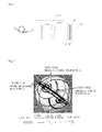
- Fig. 2 is a conceptual diagram of polarization control by means of phase modulators of 0 degree, 45 degrees and 0 degree.
- the orientations of liquid crystal LC are aligned in the order of 0 degree, 45 degrees and 0 degree.
- the wavelength selective polarization controller of the present invention is capable of rendering the linear polarized light to be in an arbitrary polarization state by using the phase modulator after having controlled the polarization plane thereof.
- the plurality of phase modulators 21, 22, 23 may be ones having a first phase modulator of 90 degrees, a second phase modulator of 135 degrees and a third phase modulator of 90 degrees in this order. That is, the phase modulator of 90 degrees may be used instead of the phase modulator of 0 degree. Likewise, the phase modulator of 135 degrees may be used instead of the phase modulator of 45 degrees.
- the wavelength selective polarization controller of the present invention thereby functions also as a monitor of polarization states.
- the wavelength selective polarization controller has a control device such as a computer or the like.
- the control device is connected to the respective phase modulators.
- the control device receives information as to control amounts from the phase modulators, and stores them in a storage portion.
- the control device reads out the information as to control amounts from the storage portion, and carries out computation for obtaining the polarization amounts in the computation portion, in response to the directions of a control program stored in the main memory.
- the control device outputs the computation results to an output portion such as a monitor or the like, besides storing them in the storage portion as appropriate.
- the wavelength selective polarization controller of the present invention thus functions also as a monitor of polarization states.
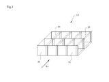
- Fig. 3 is a view showing an example of liquid crystal cells constituting a polarization controller.
- the polarization controller 12 may be one having a plurality of liquid crystal cells formed in a line shape or a matrix shape.
- the liquid crystal cells are each provided, for example, not only a liquid crystal substance but also electrodes existing so as to interpose the liquid crystal substance therebetween.
- the electrode may be a transparent electrode or a metal electrode existing at any location in a periphery of the cell.
- three pieces of a liquid crystal element having a lattice pitch of 10 ⁇ m to 40 ⁇ m are joined together, and the joined one is only mounted on a glass substrate.
- the above lattice pitch becomes a factor of determining the width of the cell. It is noted that there may be provided a gap in between the adjoining liquid crystal cells.
- one located on the side of a condenser has a convergence diameter small as much as possible because the width of an obtained band path becomes small.
- the convergence diameter one having the convergence diameter of the range from equal to or more than 20 ⁇ m to equal to or less than 80 ⁇ m is named as the convergence diameter, and one having the range from equal to or more than 30 ⁇ m to 70 ⁇ m is favorably named.
- the range from equal to or more than 10 ⁇ m to equal to or less than 40 ⁇ m is named, and the range is favorably equal to or more than 15 ⁇ m to equal to or less than 30 ⁇ m, or may be equal to or more than 15 ⁇ m to equal to or less than 25 ⁇ m. Since minute cells are thus used, a passband of, for example, 10 GHz interval can be attained.
- the convergence diameter becomes larger as the wavelength becomes larger, two liquid crystal cells may receive single light on the short wavelength side, and three liquid crystal cells may receive single light on the long wavelength side.
- the convergence diameter is a diameter of the light obtained by image-forming the plural light converged by the condenser on the liquid crystal cell.
- the telecentric optical system 11 has a second condenser 31 to which output light from the polarization controller 12 is incident, and a second diffraction grating 32 to which the output light having passed through the second condenser 31 is incident.
- the condenser 31 and diffraction grating 32 ones similar with ones described above can be used.
- the first condenser and first diffraction grating can be used as the second condenser and second diffraction grating, respectively.
- the output optical system 13 there are named, for example, one having a configuration symmetric with the telecentric optical system 11 and, in the case in which light beams return by being reflected, the telecentric optical system 11 itself. In this case, it is only required that a well-known reflector or mirror should exit. Then, by returning the light beams to an optical path after the polarization plane thereof has been controlled, it is possible to output the light beams as an optical wavelength multiplexing signal.
- Fig. 4 is a conceptual diagram showing a wavelength selective polarization controller of Embodiment 1.
- IN denotes an incident wavelength multiplexing signal.
- PMF denotes a polarization maintaining fiber.
- AL denotes a condenser.
- Pol denotes a polarization plane control device.
- GRATING denotes a diffraction grating.
- SPATIAL MODULATOR denotes a polarization controller.
- QWP denotes a quarter wavelength plate.
- MR denotes a mirror.
- SMF denotes a single-mode fiber, and OUT denotes an output signal.
- Light output from the PMF is incident to a position offset from the center of a condenser. Then, this light propagates diagonally as collimated light. The diagonally propagated light passes through a diffraction grating and is incident to another condenser.
- the light condensed by the condenser is incident to a polarization control device.
- the light subjected to control of the polarization plane in the polarization control device is incident to a condenser.
- the light exited from the condenser propagetes via a quarter wavelength plate and a mirror as collimated light, and the polarization plane then rotates 45 degrees. After that, the light of which the polarization plane has been rotated is incident to a polarization control device again and, after propagated via a symmetric optical path, is output from the SMF.
- Fig. 5 is a conceptual diagram showing a wavelength selective polarization controller of Embodiment 2. Even in the mode as shown in Fig. 5 , it is also possible to provide a similar wavelength selective polarization controller as with Embodiment 1.
- Figs. 6A and 6B are views each showing a wavelength selective polarization controller, using a polarization-independent wavelength dispersion element, of Embodiment 3 of the present invention, Fig. 6A being a view seen from the direction from which wavelength separation is comprehended, Fig. 6B being a view seen from the direction orthogonal to Fig. 6A .
- reference numeral 611 denotes an optical input fiber
- reference numeral 612 denotes an optical output fiber
- reference numeral 621 denotes a collimator lens
- reference numeral 622 denotes a condenser
- reference numeral 63 denotes a wavelength dispersion element
- reference numerals 641, 644 denotes a 0°-orientation axis liquid crystal cell
- reference numerals 642, 643 denotes a 45°-orientation axis liquid crystal cell
- reference numeral 65 denotes a beam splitter
- reference numeral 66 denotes a total reflection mirror
- reference numeral 67 denotes a polarization separation element
- reference numerals 681, 682 denotes a light receiving element
- reference numeral 691 denotes an A/D converter
- reference numeral 692 denotes an arithmetic processing circuit.
- the wavelength selective polarization controller includes a memory function of storing data, and a computer for determining and controlling the operation of liquid crystal cells on the basis of data of the arithmetic processing circuit. The operation of this embodiment will be described below.
- Optical wavelength multiplexing signal light input from a fiber 611 is collimated at the lens 621, and is subjected to a change in the angle depending on the respective wavelengths by being input to the wavelength dispersion element 63 to be input to the lens 622.
- the fiber 611, fiber 612, lens 621 and lens 622 are rendered to be a telecentric optical system on both sides, and main light beams are condensed by the lens 622 from one wavelength to another in the state of being parallel to the optical axis.
- the condensed signal light is input to liquid crystals 641 and 642.
- liquid crystals 641 and 642 there are arranged the cells of a number equal to or more than the number of wavelengths of the signal light in the wavelength separation direction, and the input liquid crystal cells are different from one wavelength to another.
- the signal light having passed through the liquid crystal 642 is input to the beam splitter 65, and the one part passes therethrough, while the other part is reflected there.
- the monitor light is separated into P-polarized light and S-polarized light components by a polarization separation element.
- the separated polarized light components are input to the light receiving elements 681 and 682, respectively.
- the light receiving elements 681 and 682 there are arranged the light receiving elements of a number equal to or more than the number of wavelengths of the signal light in the wavelength separation direction, and it is possible to obtain light intensity of each polarized light component of the monitor light from one wavelength to another.
- the light intensities obtained by the light receiving elements 681 and 682 are digitized by an A/D converter, and are subjected to comparison calculation in the arithmetic processing circuit 692, which has a function of comparing them.
- the monitor light is usually input to the light receiving elements 681 and 682 by relaying with an appropriate lens system.
- the signal light having been reflected at the beam splitter 66 has been controlled to the linear polarized light as described above, and is reflected in the state of the linear polarized light at the total reflection mirror 66.
- the signal light is input to liquid crystals 644 and 643 in the state of the linear polarized light.
- the liquid crystals 643 and 644 there are arranged the cells of a number equal to or more than the number of wavelengths of the signal light in the wavelength separation direction, the input liquid crystal cells are different from one wavelength to another.
- the signal light Since the signal light is input at the linear polarized light of 45°, 0° relatively with respect to the orientation axis of each of the liquid crystals, it is possible to control the signal light to an arbitrary polarization state from one wavelength to another by individually controlling the phase amounts of the liquid crystals 643 and 644.
- the signal light having been subjected to polarization control is collimated by the lens 622 to be incident to the wavelength dispersion element, and the respective wavelengths having been separated are remultiplexed.
- the signal light that has been subjected to polarization control from one wavelength to another and has been remultiplexed is condensed by the lens 621 and is output through the fiber 612.
- the configuration using the polarization separation element and light receiving elements is presented as a configuration of the monitor of the polarization state of signal light, it may be possible to substitute a different optical system capable of measuring the polarization state.
- a common Stokes parameter measurement optical system constituted of a beam splitter, polarization separation element, fixed phase difference element, analyzer, light receiving element, A/D converter and arithmetic processing circuit.
- Figs. 7A and 7B are views each showing a wavelength selective polarization controller, using a polarization-dependent wavelength dispersion element, of Embodiment 4 of the present invention, Fig. 7A being a view seen from the direction from which wavelength separation is comprehended, Fig. 7B being a view seen from the direction orthogonal to Fig. 7A .
- reference numerals 661 to 66 are as with described above, but the wavelength dispersion element 63 is rendered to have polarization dependence prominently.
- Reference numerals 711 to 714 each denote a polarization separation element
- reference numerals 721 to 724 each denote a half wavelength plate
- reference numeral 73 denotes a polarization dependence wavelength dispersion element
- reference numerals 741 to 744 each denote an optical path length correction plate having the same optical path length as that of each of wavelength plates 721 to 724.
- the wavelength selective polarization controller also has the monitor portion constituted of reference numerals 67 to 692 in Fig. 6A .
- Optical wavelength multiplexing signal light input from the fiber 611 is separated into a P-polarized light component and an S-polarization component by the polarization separation element 711.
- the polarized light on one side passes through the correction plate 741 and is input to the lens 621 without being treated.
- the polarized light on the other side is input to the wavelength plate 721 the optical axis of which is inclined by 45° with respect to input polarized light, and the polarization plane thereof is turned by 90°, that is, it is rendered to be the same polarized light as the polarized light on one side and is input to the lens 621.
- the two beams of signal light which have had an identical polarization plane, change the angle depending on the respective wavelengths by being collimated at the lens 621 and being input to the wavelength dispersion element 73, and is input to the lens 622 to be condensed.
- One beam of the signal light passes through the correction plate 742 and is input to the polarization separation element 712.
- the other beam of the signal light is input to the wavelength plate 722 the optical axis of which is inclined by 45° with respect to the input polarized light, and the polarization plane thereof is turned by 90°, that is, it is rendered to be polarized light orthogonal to the polarized light on one side and is input to the polarization separation element 712.
- the signal light having been separated into two beams by the polarization separation element 712 is polarization-multiplexed to be output.
- the condensed signal light is input to the liquid crystals 641 and 642.
- the liquid crystals 641 and 642 there are arranged the cells of a number equal to or more than the number of wavelengths of the signal light in the wavelength separation direction, and the input liquid crystal cells are different from one wavelength to another.
- the signal light having passed through the liquid crystal 642 is input to the beam splitter 65, and the one part passes therethrough, while the other part is reflected there.
- Embodiment 3 Thereafter, by implementing the same operation as with Embodiment 3 up to the liquid crystal 643, it is possible to control the signal light to an arbitrary polarization state from one wavelength to another on the output side of the liquid crystal 643.
- the signal light having been subjected to polarization control is separated into a P-polarized light component and an S-polarization component by the polarization separation element 713.
- the polarized light on one side passes through the correction plate 743 and is input to the lens 622.
- the polarized light on the other side is input to the wavelength plate 723 the optical axis of which is inclined by 45° with respect to the input polarized light, and the polarization plane thereof is turned by 90°, that is, it is rendered to be the same polarized light as the polarized light on one side and is input to the lens 622.
- the two beams of signal light having been subjected to polarization control and separated are wavelength-multiplexed by being collimated by the lens 622 and being input to the wavelength dispersion element 73.
- the signal light on one side having been wavelength-multiplexed is condensed by the lens 621 and passes through the correction plate 744 to be input to the polarization separation element 714.
- the signal light on the other side is condensed by the lens 621, and, by being input to the wavelength plate 724 the optical axis of which is inclined by 45° with respect to the input polarized light, the polarization plane thereof is turned by 90° to be input to the polarization separation element 714. Consequently, the two beams of signal light having been subjected to polarization control are polarization-multiplexed at the polarization separation element 714, and the signal light having been subjected to polarization control from one wavelength to another becomes one beam to be output from the fiber 612.
- the present invention can be utilized in the field of optical information communication.
Landscapes
- Physics & Mathematics (AREA)
- General Physics & Mathematics (AREA)
- Optics & Photonics (AREA)
- Nonlinear Science (AREA)
- Optical Modulation, Optical Deflection, Nonlinear Optics, Optical Demodulation, Optical Logic Elements (AREA)
- Liquid Crystal (AREA)
- Optical Communication System (AREA)
Applications Claiming Priority (2)
| Application Number | Priority Date | Filing Date | Title |
|---|---|---|---|
| JP2011132791A JP5838532B2 (ja) | 2011-06-15 | 2011-06-15 | 波長選択偏波制御器 |
| PCT/JP2012/065007 WO2012173113A1 (ja) | 2011-06-15 | 2012-06-12 | 波長選択偏波制御器 |
Publications (3)
| Publication Number | Publication Date |
|---|---|
| EP2722706A1 true EP2722706A1 (de) | 2014-04-23 |
| EP2722706A4 EP2722706A4 (de) | 2014-12-24 |
| EP2722706B1 EP2722706B1 (de) | 2020-05-20 |
Family
ID=47357100
Family Applications (1)
| Application Number | Title | Priority Date | Filing Date |
|---|---|---|---|
| EP12801085.7A Active EP2722706B1 (de) | 2011-06-15 | 2012-06-12 | Wellenlängenauswahl-polarisationssteuerung |
Country Status (6)
| Country | Link |
|---|---|
| US (1) | US8982442B2 (de) |
| EP (1) | EP2722706B1 (de) |
| JP (1) | JP5838532B2 (de) |
| CN (1) | CN103608717B (de) |
| CA (1) | CA2848178C (de) |
| WO (1) | WO2012173113A1 (de) |
Cited By (1)
| Publication number | Priority date | Publication date | Assignee | Title |
|---|---|---|---|---|
| EP3043495A4 (de) * | 2013-09-27 | 2016-09-07 | Huawei Tech Co Ltd | Wellenlängenselektiver schalter und verfahren zur steuerung eines räumlichen phasenmodulators in diesem wellenlängenselektiven schalter |
Families Citing this family (4)
| Publication number | Priority date | Publication date | Assignee | Title |
|---|---|---|---|---|
| WO2015170780A1 (ja) * | 2014-05-07 | 2015-11-12 | 国立大学法人電気通信大学 | レーザー装置 |
| JP2018205646A (ja) * | 2017-06-08 | 2018-12-27 | 大学共同利用機関法人自然科学研究機構 | 2光波の位相調整装置 |
| US11223781B2 (en) * | 2017-08-21 | 2022-01-11 | Sony Corporation | Image-capturing apparatus and image-capturing method |
| CN119574463B (zh) * | 2024-09-27 | 2025-09-19 | 西北工业大学 | 一种基于超表面的波长无关的实时偏振成像方法及装置 |
Family Cites Families (14)
| Publication number | Priority date | Publication date | Assignee | Title |
|---|---|---|---|---|
| EP0663604A1 (de) | 1994-01-03 | 1995-07-19 | AT&T Corp. | Polarisationsdrehvorrichtung |
| JPH08262394A (ja) * | 1995-03-28 | 1996-10-11 | Nippon Telegr & Teleph Corp <Ntt> | 多入力多出力光偏波コントローラ |
| JP4474625B2 (ja) * | 1999-12-14 | 2010-06-09 | 独立行政法人科学技術振興機構 | 超広帯域可変波長多重パルス波形整形装置 |
| US6529307B1 (en) * | 2000-06-05 | 2003-03-04 | Avanex Corporation | Selective intensity modulation of channels in a multiplexed optical communication system |
| WO2003032071A1 (en) * | 2001-10-09 | 2003-04-17 | Xtellus Inc. | Wavelength selective optical switch |
| US7236660B2 (en) | 2002-05-20 | 2007-06-26 | Jds Uniphase Corporation | Reconfigurable optical add-drop module, system and method |
| US7218857B1 (en) * | 2003-03-28 | 2007-05-15 | Avanex Corporation | Method, apparatus and system for a re-configurable optical add-drop multiplexer |
| US7092594B2 (en) | 2003-03-31 | 2006-08-15 | Fujitsu Limited | Wavelength selector switch |
| JP4544828B2 (ja) * | 2003-03-31 | 2010-09-15 | 富士通株式会社 | 波長選択スイッチ |
| US20080089698A1 (en) * | 2006-05-19 | 2008-04-17 | Zhi Jiang | Optical arbitrary waveform generation and processing using spectral line-by-line pulse shaping |
| JP5228205B2 (ja) * | 2007-06-15 | 2013-07-03 | 独立行政法人情報通信研究機構 | 光波形整形装置 |
| JP5125245B2 (ja) | 2007-06-15 | 2013-01-23 | 独立行政法人情報通信研究機構 | 光波形整形装置 |
| NL1036407A1 (nl) * | 2008-01-23 | 2009-07-27 | Asml Netherlands Bv | Polarization control apparatus and method. |
| CN101888280A (zh) * | 2009-05-13 | 2010-11-17 | 华为技术有限公司 | 波长选择装置及方法、波长复用设备 |
-
2011
- 2011-06-15 JP JP2011132791A patent/JP5838532B2/ja active Active
-
2012
- 2012-06-12 WO PCT/JP2012/065007 patent/WO2012173113A1/ja not_active Ceased
- 2012-06-12 EP EP12801085.7A patent/EP2722706B1/de active Active
- 2012-06-12 CA CA2848178A patent/CA2848178C/en active Active
- 2012-06-12 US US14/126,161 patent/US8982442B2/en active Active
- 2012-06-12 CN CN201280029597.1A patent/CN103608717B/zh not_active Expired - Fee Related
Cited By (2)
| Publication number | Priority date | Publication date | Assignee | Title |
|---|---|---|---|---|
| EP3043495A4 (de) * | 2013-09-27 | 2016-09-07 | Huawei Tech Co Ltd | Wellenlängenselektiver schalter und verfahren zur steuerung eines räumlichen phasenmodulators in diesem wellenlängenselektiven schalter |
| US9660723B2 (en) | 2013-09-27 | 2017-05-23 | Huawei Technologies Co., Ltd. | Wavelength selective switch and method for controlling spatial phase modulator in wavelengths |
Also Published As
| Publication number | Publication date |
|---|---|
| EP2722706A4 (de) | 2014-12-24 |
| CA2848178C (en) | 2019-08-27 |
| CN103608717A (zh) | 2014-02-26 |
| JP5838532B2 (ja) | 2016-01-06 |
| US20140133004A1 (en) | 2014-05-15 |
| JP2013003277A (ja) | 2013-01-07 |
| WO2012173113A1 (ja) | 2012-12-20 |
| CN103608717B (zh) | 2016-10-05 |
| CA2848178A1 (en) | 2012-12-20 |
| EP2722706B1 (de) | 2020-05-20 |
| US8982442B2 (en) | 2015-03-17 |
Similar Documents
| Publication | Publication Date | Title |
|---|---|---|
| EP2875393B1 (de) | Polarisationsdiverser, wellenselektiver schalter | |
| US8982442B2 (en) | Wavelength selection polarization controller | |
| EP2169448B1 (de) | Anordnung zur formung einer optischen signalform | |
| EP3266132B1 (de) | Optische anordnung zur verwaltung der diversität und isolation zwischen anschlüssen in einem wellenlängenselektiven schalter | |
| KR100258183B1 (ko) | 채널간 지연보상형 다파장 채널 투과 광필터 | |
| Jung et al. | Tunable fiber comb filter based on simple waveplate combination and polarization-diversified loop | |
| CN120352984B (zh) | 一种基于硅基液晶的光交叉系统及控制方法 | |
| WO2016144572A1 (en) | Architecture for all-fiber delivery of coherently combined laser power | |
| US7072113B2 (en) | Wavelength selective switching device and method for selectively transmitting optical signals based on wavelength | |
| JP4546959B2 (ja) | 偏波保持導波路コンポーネントに入力される光の偏波を制御するための適応的偏波調整装置 | |
| JP5669140B2 (ja) | 光パフォーマンスモニタ | |
| CN119137516A (zh) | 集成偏振控制器系统 | |
| US20050270529A1 (en) | Stokes parameter measurement device and method | |
| JP2003083810A (ja) | 分光装置および光測定装置 | |
| JP5839586B2 (ja) | 光信号処理装置 | |
| Kim et al. | Inline selection of transmission or reflection spectra of different fiber Bragg gratings using polarization-diversity loop | |
| US20250286644A1 (en) | Optical channel monitor assisted by a switching engine | |
| JP5681598B2 (ja) | 偏波モード分散発生装置 | |
| JP2003307717A (ja) | 光信号処理装置 | |
| US20020154405A1 (en) | Cylindrical polarization diversity asembly |
Legal Events
| Date | Code | Title | Description |
|---|---|---|---|
| PUAI | Public reference made under article 153(3) epc to a published international application that has entered the european phase |
Free format text: ORIGINAL CODE: 0009012 |
|
| 17P | Request for examination filed |
Effective date: 20131216 |
|
| AK | Designated contracting states |
Kind code of ref document: A1 Designated state(s): AL AT BE BG CH CY CZ DE DK EE ES FI FR GB GR HR HU IE IS IT LI LT LU LV MC MK MT NL NO PL PT RO RS SE SI SK SM TR |
|
| RAP1 | Party data changed (applicant data changed or rights of an application transferred) |
Owner name: NATIONAL INSTITUTE OF INFORMATION AND COMMUNICATIO |
|
| DAX | Request for extension of the european patent (deleted) | ||
| A4 | Supplementary search report drawn up and despatched |
Effective date: 20141120 |
|
| RIC1 | Information provided on ipc code assigned before grant |
Ipc: G02F 1/01 20060101AFI20141114BHEP |
|
| 17Q | First examination report despatched |
Effective date: 20160208 |
|
| STAA | Information on the status of an ep patent application or granted ep patent |
Free format text: STATUS: EXAMINATION IS IN PROGRESS |
|
| GRAP | Despatch of communication of intention to grant a patent |
Free format text: ORIGINAL CODE: EPIDOSNIGR1 |
|
| STAA | Information on the status of an ep patent application or granted ep patent |
Free format text: STATUS: GRANT OF PATENT IS INTENDED |
|
| INTG | Intention to grant announced |
Effective date: 20191206 |
|
| GRAS | Grant fee paid |
Free format text: ORIGINAL CODE: EPIDOSNIGR3 |
|
| GRAA | (expected) grant |
Free format text: ORIGINAL CODE: 0009210 |
|
| STAA | Information on the status of an ep patent application or granted ep patent |
Free format text: STATUS: THE PATENT HAS BEEN GRANTED |
|
| AK | Designated contracting states |
Kind code of ref document: B1 Designated state(s): AL AT BE BG CH CY CZ DE DK EE ES FI FR GB GR HR HU IE IS IT LI LT LU LV MC MK MT NL NO PL PT RO RS SE SI SK SM TR |
|
| REG | Reference to a national code |
Ref country code: GB Ref legal event code: FG4D |
|
| REG | Reference to a national code |
Ref country code: CH Ref legal event code: EP |
|
| REG | Reference to a national code |
Ref country code: DE Ref legal event code: R096 Ref document number: 602012070247 Country of ref document: DE |
|
| REG | Reference to a national code |
Ref country code: AT Ref legal event code: REF Ref document number: 1272981 Country of ref document: AT Kind code of ref document: T Effective date: 20200615 |
|
| REG | Reference to a national code |
Ref country code: LT Ref legal event code: MG4D |
|
| REG | Reference to a national code |
Ref country code: NL Ref legal event code: MP Effective date: 20200520 |
|
| PG25 | Lapsed in a contracting state [announced via postgrant information from national office to epo] |
Ref country code: LT Free format text: LAPSE BECAUSE OF FAILURE TO SUBMIT A TRANSLATION OF THE DESCRIPTION OR TO PAY THE FEE WITHIN THE PRESCRIBED TIME-LIMIT Effective date: 20200520 Ref country code: GR Free format text: LAPSE BECAUSE OF FAILURE TO SUBMIT A TRANSLATION OF THE DESCRIPTION OR TO PAY THE FEE WITHIN THE PRESCRIBED TIME-LIMIT Effective date: 20200821 Ref country code: SE Free format text: LAPSE BECAUSE OF FAILURE TO SUBMIT A TRANSLATION OF THE DESCRIPTION OR TO PAY THE FEE WITHIN THE PRESCRIBED TIME-LIMIT Effective date: 20200520 Ref country code: NO Free format text: LAPSE BECAUSE OF FAILURE TO SUBMIT A TRANSLATION OF THE DESCRIPTION OR TO PAY THE FEE WITHIN THE PRESCRIBED TIME-LIMIT Effective date: 20200820 Ref country code: IS Free format text: LAPSE BECAUSE OF FAILURE TO SUBMIT A TRANSLATION OF THE DESCRIPTION OR TO PAY THE FEE WITHIN THE PRESCRIBED TIME-LIMIT Effective date: 20200920 Ref country code: FI Free format text: LAPSE BECAUSE OF FAILURE TO SUBMIT A TRANSLATION OF THE DESCRIPTION OR TO PAY THE FEE WITHIN THE PRESCRIBED TIME-LIMIT Effective date: 20200520 Ref country code: PT Free format text: LAPSE BECAUSE OF FAILURE TO SUBMIT A TRANSLATION OF THE DESCRIPTION OR TO PAY THE FEE WITHIN THE PRESCRIBED TIME-LIMIT Effective date: 20200921 |
|
| PG25 | Lapsed in a contracting state [announced via postgrant information from national office to epo] |
Ref country code: HR Free format text: LAPSE BECAUSE OF FAILURE TO SUBMIT A TRANSLATION OF THE DESCRIPTION OR TO PAY THE FEE WITHIN THE PRESCRIBED TIME-LIMIT Effective date: 20200520 Ref country code: LV Free format text: LAPSE BECAUSE OF FAILURE TO SUBMIT A TRANSLATION OF THE DESCRIPTION OR TO PAY THE FEE WITHIN THE PRESCRIBED TIME-LIMIT Effective date: 20200520 Ref country code: BG Free format text: LAPSE BECAUSE OF FAILURE TO SUBMIT A TRANSLATION OF THE DESCRIPTION OR TO PAY THE FEE WITHIN THE PRESCRIBED TIME-LIMIT Effective date: 20200820 Ref country code: RS Free format text: LAPSE BECAUSE OF FAILURE TO SUBMIT A TRANSLATION OF THE DESCRIPTION OR TO PAY THE FEE WITHIN THE PRESCRIBED TIME-LIMIT Effective date: 20200520 |
|
| REG | Reference to a national code |
Ref country code: AT Ref legal event code: MK05 Ref document number: 1272981 Country of ref document: AT Kind code of ref document: T Effective date: 20200520 |
|
| PG25 | Lapsed in a contracting state [announced via postgrant information from national office to epo] |
Ref country code: AL Free format text: LAPSE BECAUSE OF FAILURE TO SUBMIT A TRANSLATION OF THE DESCRIPTION OR TO PAY THE FEE WITHIN THE PRESCRIBED TIME-LIMIT Effective date: 20200520 Ref country code: NL Free format text: LAPSE BECAUSE OF FAILURE TO SUBMIT A TRANSLATION OF THE DESCRIPTION OR TO PAY THE FEE WITHIN THE PRESCRIBED TIME-LIMIT Effective date: 20200520 |
|
| PG25 | Lapsed in a contracting state [announced via postgrant information from national office to epo] |
Ref country code: CZ Free format text: LAPSE BECAUSE OF FAILURE TO SUBMIT A TRANSLATION OF THE DESCRIPTION OR TO PAY THE FEE WITHIN THE PRESCRIBED TIME-LIMIT Effective date: 20200520 Ref country code: RO Free format text: LAPSE BECAUSE OF FAILURE TO SUBMIT A TRANSLATION OF THE DESCRIPTION OR TO PAY THE FEE WITHIN THE PRESCRIBED TIME-LIMIT Effective date: 20200520 Ref country code: ES Free format text: LAPSE BECAUSE OF FAILURE TO SUBMIT A TRANSLATION OF THE DESCRIPTION OR TO PAY THE FEE WITHIN THE PRESCRIBED TIME-LIMIT Effective date: 20200520 Ref country code: EE Free format text: LAPSE BECAUSE OF FAILURE TO SUBMIT A TRANSLATION OF THE DESCRIPTION OR TO PAY THE FEE WITHIN THE PRESCRIBED TIME-LIMIT Effective date: 20200520 Ref country code: DK Free format text: LAPSE BECAUSE OF FAILURE TO SUBMIT A TRANSLATION OF THE DESCRIPTION OR TO PAY THE FEE WITHIN THE PRESCRIBED TIME-LIMIT Effective date: 20200520 Ref country code: AT Free format text: LAPSE BECAUSE OF FAILURE TO SUBMIT A TRANSLATION OF THE DESCRIPTION OR TO PAY THE FEE WITHIN THE PRESCRIBED TIME-LIMIT Effective date: 20200520 Ref country code: SM Free format text: LAPSE BECAUSE OF FAILURE TO SUBMIT A TRANSLATION OF THE DESCRIPTION OR TO PAY THE FEE WITHIN THE PRESCRIBED TIME-LIMIT Effective date: 20200520 Ref country code: IT Free format text: LAPSE BECAUSE OF FAILURE TO SUBMIT A TRANSLATION OF THE DESCRIPTION OR TO PAY THE FEE WITHIN THE PRESCRIBED TIME-LIMIT Effective date: 20200520 |
|
| REG | Reference to a national code |
Ref country code: CH Ref legal event code: PL |
|
| REG | Reference to a national code |
Ref country code: DE Ref legal event code: R097 Ref document number: 602012070247 Country of ref document: DE |
|
| PG25 | Lapsed in a contracting state [announced via postgrant information from national office to epo] |
Ref country code: PL Free format text: LAPSE BECAUSE OF FAILURE TO SUBMIT A TRANSLATION OF THE DESCRIPTION OR TO PAY THE FEE WITHIN THE PRESCRIBED TIME-LIMIT Effective date: 20200520 Ref country code: MC Free format text: LAPSE BECAUSE OF FAILURE TO SUBMIT A TRANSLATION OF THE DESCRIPTION OR TO PAY THE FEE WITHIN THE PRESCRIBED TIME-LIMIT Effective date: 20200520 Ref country code: SK Free format text: LAPSE BECAUSE OF FAILURE TO SUBMIT A TRANSLATION OF THE DESCRIPTION OR TO PAY THE FEE WITHIN THE PRESCRIBED TIME-LIMIT Effective date: 20200520 |
|
| PLBE | No opposition filed within time limit |
Free format text: ORIGINAL CODE: 0009261 |
|
| STAA | Information on the status of an ep patent application or granted ep patent |
Free format text: STATUS: NO OPPOSITION FILED WITHIN TIME LIMIT |
|
| PG25 | Lapsed in a contracting state [announced via postgrant information from national office to epo] |
Ref country code: LU Free format text: LAPSE BECAUSE OF NON-PAYMENT OF DUE FEES Effective date: 20200612 |
|
| REG | Reference to a national code |
Ref country code: BE Ref legal event code: MM Effective date: 20200630 |
|
| 26N | No opposition filed |
Effective date: 20210223 |
|
| PG25 | Lapsed in a contracting state [announced via postgrant information from national office to epo] |
Ref country code: LI Free format text: LAPSE BECAUSE OF NON-PAYMENT OF DUE FEES Effective date: 20200630 Ref country code: IE Free format text: LAPSE BECAUSE OF NON-PAYMENT OF DUE FEES Effective date: 20200612 Ref country code: CH Free format text: LAPSE BECAUSE OF NON-PAYMENT OF DUE FEES Effective date: 20200630 |
|
| PG25 | Lapsed in a contracting state [announced via postgrant information from national office to epo] |
Ref country code: SI Free format text: LAPSE BECAUSE OF FAILURE TO SUBMIT A TRANSLATION OF THE DESCRIPTION OR TO PAY THE FEE WITHIN THE PRESCRIBED TIME-LIMIT Effective date: 20200520 Ref country code: BE Free format text: LAPSE BECAUSE OF NON-PAYMENT OF DUE FEES Effective date: 20200630 |
|
| PGFP | Annual fee paid to national office [announced via postgrant information from national office to epo] |
Ref country code: DE Payment date: 20210618 Year of fee payment: 10 Ref country code: FR Payment date: 20210622 Year of fee payment: 10 |
|
| PGFP | Annual fee paid to national office [announced via postgrant information from national office to epo] |
Ref country code: GB Payment date: 20210625 Year of fee payment: 10 |
|
| PG25 | Lapsed in a contracting state [announced via postgrant information from national office to epo] |
Ref country code: TR Free format text: LAPSE BECAUSE OF FAILURE TO SUBMIT A TRANSLATION OF THE DESCRIPTION OR TO PAY THE FEE WITHIN THE PRESCRIBED TIME-LIMIT Effective date: 20200520 Ref country code: MT Free format text: LAPSE BECAUSE OF FAILURE TO SUBMIT A TRANSLATION OF THE DESCRIPTION OR TO PAY THE FEE WITHIN THE PRESCRIBED TIME-LIMIT Effective date: 20200520 Ref country code: CY Free format text: LAPSE BECAUSE OF FAILURE TO SUBMIT A TRANSLATION OF THE DESCRIPTION OR TO PAY THE FEE WITHIN THE PRESCRIBED TIME-LIMIT Effective date: 20200520 |
|
| PG25 | Lapsed in a contracting state [announced via postgrant information from national office to epo] |
Ref country code: MK Free format text: LAPSE BECAUSE OF FAILURE TO SUBMIT A TRANSLATION OF THE DESCRIPTION OR TO PAY THE FEE WITHIN THE PRESCRIBED TIME-LIMIT Effective date: 20200520 |
|
| REG | Reference to a national code |
Ref country code: DE Ref legal event code: R119 Ref document number: 602012070247 Country of ref document: DE |
|
| GBPC | Gb: european patent ceased through non-payment of renewal fee |
Effective date: 20220612 |
|
| PG25 | Lapsed in a contracting state [announced via postgrant information from national office to epo] |
Ref country code: FR Free format text: LAPSE BECAUSE OF NON-PAYMENT OF DUE FEES Effective date: 20220630 |
|
| PG25 | Lapsed in a contracting state [announced via postgrant information from national office to epo] |
Ref country code: GB Free format text: LAPSE BECAUSE OF NON-PAYMENT OF DUE FEES Effective date: 20220612 Ref country code: DE Free format text: LAPSE BECAUSE OF NON-PAYMENT OF DUE FEES Effective date: 20230103 |