EP2721906B1 - Einzelschalter-antriebsvorrichtung mit einem lc-filter zum antreiben einer last, insbesondere einer led-einheit - Google Patents
Einzelschalter-antriebsvorrichtung mit einem lc-filter zum antreiben einer last, insbesondere einer led-einheit Download PDFInfo
- Publication number
- EP2721906B1 EP2721906B1 EP12732709.6A EP12732709A EP2721906B1 EP 2721906 B1 EP2721906 B1 EP 2721906B1 EP 12732709 A EP12732709 A EP 12732709A EP 2721906 B1 EP2721906 B1 EP 2721906B1
- Authority
- EP
- European Patent Office
- Prior art keywords
- coupled
- driver device
- power
- voltage
- output terminal
- Prior art date
- Legal status (The legal status is an assumption and is not a legal conclusion. Google has not performed a legal analysis and makes no representation as to the accuracy of the status listed.)
- Active
Links
Images


Classifications
-
- H—ELECTRICITY
- H05—ELECTRIC TECHNIQUES NOT OTHERWISE PROVIDED FOR
- H05B—ELECTRIC HEATING; ELECTRIC LIGHT SOURCES NOT OTHERWISE PROVIDED FOR; CIRCUIT ARRANGEMENTS FOR ELECTRIC LIGHT SOURCES, IN GENERAL
- H05B45/00—Circuit arrangements for operating light-emitting diodes [LED]
- H05B45/30—Driver circuits
- H05B45/37—Converter circuits
- H05B45/3725—Switched mode power supply [SMPS]
- H05B45/375—Switched mode power supply [SMPS] using buck topology
-
- H—ELECTRICITY
- H05—ELECTRIC TECHNIQUES NOT OTHERWISE PROVIDED FOR
- H05B—ELECTRIC HEATING; ELECTRIC LIGHT SOURCES NOT OTHERWISE PROVIDED FOR; CIRCUIT ARRANGEMENTS FOR ELECTRIC LIGHT SOURCES, IN GENERAL
- H05B45/00—Circuit arrangements for operating light-emitting diodes [LED]
- H05B45/30—Driver circuits
- H05B45/37—Converter circuits
- H05B45/3725—Switched mode power supply [SMPS]
- H05B45/385—Switched mode power supply [SMPS] using flyback topology
-
- Y—GENERAL TAGGING OF NEW TECHNOLOGICAL DEVELOPMENTS; GENERAL TAGGING OF CROSS-SECTIONAL TECHNOLOGIES SPANNING OVER SEVERAL SECTIONS OF THE IPC; TECHNICAL SUBJECTS COVERED BY FORMER USPC CROSS-REFERENCE ART COLLECTIONS [XRACs] AND DIGESTS
- Y02—TECHNOLOGIES OR APPLICATIONS FOR MITIGATION OR ADAPTATION AGAINST CLIMATE CHANGE
- Y02B—CLIMATE CHANGE MITIGATION TECHNOLOGIES RELATED TO BUILDINGS, e.g. HOUSING, HOUSE APPLIANCES OR RELATED END-USER APPLICATIONS
- Y02B20/00—Energy efficient lighting technologies, e.g. halogen lamps or gas discharge lamps
- Y02B20/30—Semiconductor lamps, e.g. solid state lamps [SSL] light emitting diodes [LED] or organic LED [OLED]
Definitions
- the present invention relates to driver device for driving a load, in particular an LED unit comprising one or more LEDs. Further, the present invention relates to a light apparatus.
- two series connected power stages are employed to obtain high power factor while keeping the output power constant throughout a mains cycle (or supply cycle, i.e. the cycle of the mains voltage or the supply voltage).
- the first stage shapes the mains' current and the second stage performs the power conversion to the load.
- An intermediate solution laying half-way between the two-stage and single-stage approaches is the single-stage converter with integrated preconditioner.
- Such a solution can feature reduced component count and high power density while keeping compliance with both load and power mains requirements.
- Other embodiments with a single power converting stage allow high power factor (HPF) by means of integrating a boost converter operating in discontinuous conduction mode. These converters actually combine the above mentioned two power conversion stages.
- HPF high power factor
- a HPF converter for compact fluorescent lamps is described in "High-Power-Factor Electronic Ballast with Constant DC-Link Voltage", by Ricardo de Oliveira Brioschi and Jose Luiz F. Vieira, IEEE Transactions on Power Electronics, vol. 13, no. 6, 1998 .
- a half bridge is shared by a boost converter and an LC parallel resonant converter, which is operated above resonance in order to obtain zero voltage switching (ZVS).
- ZVS zero voltage switching
- the bus voltage is controlled constant.
- Such a HPF converter typically requires a large bus capacitor and an output rectifier and has only narrow supply voltage and load (drive) voltage ranges.
- EP 2299569 discloses a driver device for receiving a rectified supply voltage from an external power supply and for providing a drive voltage and/or current for driving a load.
- the driver comprises a power conversion unit with a single switching element and an energy storage element.
- the driver comprises a control unit for controlling the switching element.
- the filter unit includes a filter inductor and a filter capacitor.
- a driver device comprising:
- a light apparatus comprising a light assembly comprising one or more light units, in particular an LED unit comprising one or more LEDs, and a driver device for driving said light assembly as provided according to the present invention.
- the present invention is based on the idea to provide a single-stage power converter (i.e. the power conversion unit) with an integrated preconditioner that feature high power factor while delivering constant output power to the load. Only a few components are required, among which half/full bridge units and large electrolytic capacitors are avoided. This is achieved by properly controlling the power converter integrated with a low-pass filter represented by elements of the filter unit. Generally, only a single switch is required to perform the conversion function.
- the proposed driver device is particularly targeted for off-line LED drivers employing high voltage LED strings coupled to the power output terminals.
- a large low frequency capacitor can be omitted by allowing a smaller low frequency storage capacitor voltage vary during the supply cycle or mains cycle (e.g. 20 ... 80%) still while keeping the output current constant. This in turn translates into smaller size, longer lifetime and more reliable, particularly at high temperature operation. Further, reduced component count is needed compromising the requirements of neither power mains nor load. This is achieved intrinsically by the operation of the power stage with integrated preconditioning function. Still further, even with the use of a large low frequency storage capacitor, single stages may not fully eliminate perceptive flicker. The proposed solution enables constant output current and hence perceptive flicker can be minimized.
- the power conversion unit there are various basic configurations of the power conversion unit provided as different embodiments that cope with various load and input voltage ranges. All of them can be controlled over full load range down to virtually zero load current by means of manipulating the duty cycle only or the switching frequency or by burst mode operation.
- the supply voltage may be a rectified periodic supply voltage provided by a power supply.
- a rectifier unit is used (as part of the driver device or as an external unit coupled to the power input terminals) for rectifying a provided AC input voltage, e.g. a mains voltage, into the (rectified periodic) supply voltage.
- a rectifier unit may, for instance, comprise a generally known half-wave or full-wave rectifier.
- the supply voltage thus has the same polarity for either polarity of the AC input voltage.
- rectified periodic supply voltage is already provided at the power input terminals, e.g. from a rectifier (representing said external power supply) provided elsewhere, no further or only general elements (like e.g. an amplifier) are coupled to the power input terminals for shaping the provided supply voltage.
- said filter inductor and said filter capacitor are coupled in series, wherein a high voltage terminal of said filter unit is coupled to said switch node.
- a low voltage terminal of said filter unit is, in one embodiment, coupled to a reference potential, in particular a ground potential and/or a power input terminal coupled to a power output terminal. In another embodiment the low voltage terminal of said filter unit is coupled to a power output terminal that is not connected to a power input terminal.
- the voltage and current stresses in devices from the converter may differ. The best options may depend on the type of components available in each case.
- the single stage power conversion unit may comprise a Cuk-type, SEPIC-type or Zeta-type converter.
- a fundamental description of the basic Cuk, SEPIC, Zeta topologies is provided by Chi K. Tse, in "Zero-order switching networks and their applications to power factor correction in switching converters", IEEE Transactions on Circuits and Systems I: Fundamental theory and applications, vol.44, no.8, August 1997 .
- said single stage power conversion unit comprises a Cuk-type converter including a first inductor coupled between a first power input terminal and the switch node, said energy storage element, in particular an intermediate capacitor, coupled between said switch node and an intermediate node, a second inductor coupled between said intermediate node and a first power output terminal, and a diode coupled between said intermediate node and a second power output terminal.
- said single stage power conversion unit comprises a SEPIC-type converter including a first inductor coupled between a first power input terminal and the switch node, said energy storage element, in particular an intermediate capacitor, coupled between said switch node and an intermediate node, a diode coupled between said intermediate node and a first power output terminal, and a second inductor coupled between said intermediate node and a second power output terminal.
- SEPIC-type converter including a first inductor coupled between a first power input terminal and the switch node, said energy storage element, in particular an intermediate capacitor, coupled between said switch node and an intermediate node, a diode coupled between said intermediate node and a first power output terminal, and a second inductor coupled between said intermediate node and a second power output terminal.
- said switching element is coupled between said switch node and a second power input terminal.
- said single stage power conversion unit comprises a Zeta-type converter including said switching element coupled between a first power input terminal and the switch node, a first inductor coupled between the switch node and a second power input terminal, a first diode coupled in series to said first inductor, said energy storage element, in particular an intermediate capacitor, coupled between said switch node and an intermediate node, a second inductor coupled between said intermediate node and a first power output terminal, and a second diode coupled between said intermediate node and a second power output terminal.
- This embodiment provides the advantages of a low output ripple and a ground referenced output.
- the various embodiments are provided for use in different applications and different voltages, and are directed to achieve certain aims. Often, a trade-off is to be made to select the optimum embodiment.
- an input decoupling capacitor coupled between the power input terminals and/or an output decoupling capacitor coupled between the power output terminals are additionally provided for high frequency decoupling.
- the switching element can be implemented in various ways, e.g. including transistors (e.g. MOSFETs) or other controlled switching means.
- transistors e.g. MOSFETs
- other controlled switching means e.g. including transistors (e.g. MOSFETs) or other controlled switching means.
- the control unit is adapted for keeping the output current constant, to keep the voltage across the energy storage element below a predetermined threshold and/or to shape the input current.
- Zero voltage switching of the switching elements is arranged for by the design (components) of the proposed driver device.
- the tasks of the control are keeping the output current constant; possibly according to a reference current (set point), to keep the bus voltage (i.e. the voltage across the energy storage element) below a preset limit and/or to shape the input current.
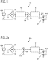
- Said driver device 10 comprises a rectifier unit 12, a first stage preconditioning unit 14 coupled to the output of the rectifier unit 12, a second stage conversion unit 16 coupled to the output of the first stage preconditioning unit 14 and a charge capacitor 18 coupled to the node 15 between said first stage preconditioning unit 14 and said second stage conversion unit 16.
- the rectifier unit 12 preferably comprises a rectifier unit, such as a known full-wave or half-wave rectifier, for rectifying an AC input voltage V20 provided, e.g., from an external mains voltage supply 20 into a rectified voltage V12.
- the load 22 is, in this embodiment, an LED unit comprising two LEDs 23 is coupled to the output of the second stage conversion unit 16 whose output signal, in particular its drive voltage V16 and its drive current I16, is used to drive the load 22.
- the first stage preconditioning unit 14 preconditions the rectified voltage V12 into an intermediate DC voltage V14
- the second stage conversion unit 16 converts said intermediate DC voltage V14 into the desired DC drive voltage V16.
- the charge capacitor 18 is provided to store a charge, i.e. is charged from the intermediate DC voltage V14, thereby filtering the low frequency signal of the rectified voltage V12 to ensure a substantially constant output signal of the second stage conversion unit 16, in particular a constant drive current I16 through the load 22.
- These elements 14, 16, 18 are generally known and widely used in such driver devices 10 and thus shall not be described in more detail here.
- the driver device 10 complies with the aforementioned demand of high power factor and low flicker at the expense of larger space requirements and cost, which might be drastically limited particularly in retrofit applications.
- the size of the first stage preconditioning unit 14 may be mainly determined by the associated passive components, particularly if it comprises a switched mode power supply (SMPS), e.g. a boost converter, operating at low or moderated switching frequency. Any attempt to increase the switching frequency so as to reduce the size of these filter components may yield a rapid increase of energy losses in the hard-switched SMPS and hence the need of use of larger heatsinks.
- SMPS switched mode power supply
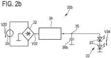
- Embodiments of known single stage driver devices 30a, 30b are schematically shown in Fig. 2a and Fig. 2b .
- Said driver device 30 comprises a rectifier unit 32 (that may be identical to the rectifier unit 12 of the two stage driver device 10 shown in Fig. 1 ) and a conversion unit 34 (e.g. flyback converter for the embodiment shown in Fig. 2b or a buck converter for the embodiment shown in Fig. 2a ) coupled to the output of the rectifier unit 32.
- a charge capacitor 36a (representing a low frequency input storage capacitor) is coupled to the node 33 between said rectifier unit 32 and said conversion unit 34 is provided.
- the charge capacitor 36b (representing a low frequency output storage capacitor) is coupled to the node 35 between said conversion unit 34 and the load 22.
- the rectifier unit rectifies an AC input voltage V20 provided, e.g., from an external mains voltage supply (also called power supply) 20 into a rectified voltage V32.
- the rectified voltage V32 is converted into the desired DC drive voltage V34 for driving the load 22.
- the storage capacitors 18 (in Fig. 1 ) and 36a, 36b (in Figs. 2a , 2b ) are mainly provided to filter out the low frequency component of the rectified voltage V12 in order to allow for a constant current into the load. Such capacitors are therefore large, particularly when placed in parallel to the load and when such load is an LED.
- Figs. 1 and 2 are, for instance, described in Robert Erickson and Michael Madigan, "Design of a simple high-power-factor rectifier based on the flyback converter", IEEE Proceedings of the Applied Power Electronics Conferences and Expositions, 1990, pp. 792-801 .
- single stage driver devices 30a, b can, although featuring a lower number of hardware components compared to two stage driver devices as exemplarily shown in Fig. 1 , generally not offer a high power factor and a low perceptible flicker simultaneously due to limitations in the size of the charge capacitor, which must filter out the low frequency component of the AC input voltage.
- single stage driver devices may critically compromise the size, the lifetime and the maximum temperature operation of the load (e.g. a lamp) due to the use of large storage capacitors used to mitigate perceptible flicker.
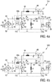
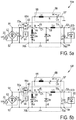
- Figs. 3 to 5 depict several embodiments of three different basic configurations of a driver device according to the present invention.
- Each configuration (embodiments of configuration 1 being shown in Fig. 3 , embodiments of configuration 2 being shown in Fig. 4 , embodiments of configuration 3 being shown in Fig. 5 ) is represented by two different embodiments of the proposed driver device including a single-stage power conversion unit and a filter unit.
- the filter capacitor also called low frequency storage capacitor
- a boost inductor Lm of the power conversion unit is designed for discontinuous conduction mode, for which purpose an additional diode (Dm) is coupled in series to said boost inductor in an embodiment.
- Dm additional diode
- all configurations are suitable for high voltage loads, e.g. high voltage strings of LEDs, but low voltage is also possible.
- the capacitor voltage can be controlled to be maintained constant by varying the switching frequency. The switching frequency increases as the output current decreases.
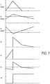
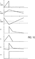
- the diagrams shown in Figs. 6 to 10 refer to the three configurations shown in Figs. 3 , 4 and 5 . They illustrate both low frequency steady-state waveforms ( Figs. 6 , 8 , 9 ) and high frequency switching waveforms ( Figs. 7 , 10 ) of the first, third and fifth embodiments shown in Figs. 3a , 4a , 5a .
- the switching waveforms of the embodiments 50b and 50d are equivalent so that the switching waveforms of embodiment 50d are not shown again separately.
- an LED load including a series connection of LED units is chosen to operate at 10W constant power, meaning that the output current must be constant.
- the rectified AC input signal refers to the European mains. Other type of loads and power supplies are possible as well.
- the resulting power factor (or PF) is higher than or equal to 90%, whereas the total harmonic distortion (or THD) is lower than 40%.
- duty cycle refers to the switch operation, e.g. 100% duty cycle implies that the switching element 60 is always on (closed).
- the switched node voltage is represented by vx.
- a first embodiment of a driver device 50a according to the present invention is schematically shown in Fig. 3a . It comprises power input terminals 51, 52 for receiving a rectified supply voltage vr from an external power supply 20 (e.g. a mains voltage supply providing a mains voltage vm) which is rectified by a rectifier 62.
- the driver device 50a further comprises power output terminals 53, 54 for providing a drive voltage vo and/or current io for driving a load 22.
- the current io is the current through the load 22 in this embodiment (as well as in the below explained embodiments shown in Figs. 4a , 5a ), which this is not the case for the other embodiments.
- the driver device 50a comprises a single stage power conversion unit 66a coupled with its input terminals 70a, 70b to the power input terminals 51, 52 and with its output terminals 70c, 70d to the power output terminals 53, 54.
- Said power conversion unit 66a comprises a single switching element 60 and an energy storage element Ch, in particular a single capacitor, both coupled to a switch node 55.
- the driver device 30a comprises a filter unit 68 comprising a filter inductor Lc and a filter capacitor Cs.
- the high voltage terminal 56 (connected to the filter inductor Lc) of said filter unit 68 is coupled to said switch node 55, while the low voltage terminal 57 (connected to the filter capacitor Cs) of said filter unit 68 is coupled to ground.
- a control unit 64 (e.g. a controller, processor or computer that is appropriately designed or programmed) is provided for controlling said switching element 60.
- an (optional) input decoupling capacitor Cm (see Fig. 5 ; not shown in Figs. 3 and 4 ), coupled between the power input terminals 51, 52 and an (optional) output decoupling capacitor Co coupled between the power output terminals 53, 54 are additionally provided in the embodiments.
- the low power input terminal 52 and the high power output terminal 53 are both coupled to ground.
- the Cuk-type power conversion unit 66a comprises a first inductor Lm coupled between the high power input terminal 51 and the switch node 55.
- the energy storage element Ch in particular an intermediate capacitor, is coupled between said switch node 55 and an intermediate node 58.
- a second inductor Lo is coupled between said intermediate node 58 and a first power output terminal 54.
- a diode Do is coupled between said intermediate node 58 and the low power output terminal 54.
- the switching element 60 is coupled between said switch node 55 and the low power input terminal 52.
- a second embodiment of a driver device 50b according to the present invention is schematically shown in Fig. 3b .
- the low voltage terminal 57 of said filter unit 68 is coupled to the low power output terminal 54 and not to ground.
- the other elements and couplings are the same as in the first embodiment of the driver device 50a.
- the circuit combines a power converter of the Cuk-type with a low-pass filter including a series connection of a high frequency filter inductor Lc and a low frequency (mains frequency) storage capacitor Cs, which is connected between switch node 55 and the load (in case of the second embodiment) or between switch node 55 and ground (in case of the first embodiment). Differences in performance and stress voltages across capacitors and switch can be relevant between both embodiments.
- the output inductor current io carries both the output load current and the storage capacitor current.
- Maximum stress voltage across the switching element 60 is the voltage across the capacitor Ch, which equals Vo/d, where d represents the duty cycle.
- the storage capacitor voltage vc is generally higher than the mains rectifier voltage vr and the output load voltage vo.
- the average input current ir(av) equals zero at the zero crossings of the rectified mains voltage vr.
- the duty cycle d is proportional to the output load voltage vo and inversely proportional to the storage capacitor voltage vc.
- Fig. 7 shows the high switching frequency waveforms at time 3ms after the zero crossing of the mains cycle voltage.
- Fig. 7 reveals the discontinuous conduction operation mode of the input current ir. Continuous conduction mode is guaranteed at the output since diode current id is always present during the off time of the switch 60. This however is not necessary and discontinuous conduction mode at the output may be allowed.
- the storage capacitor Cs can be as low as 1 ⁇ F (i.e. 100nF/W) while guaranteeing a constant output power and a high power factor.
- the load voltage vo can be substantially lower than the supply peak voltage (e.g. 70V in case of US mains supply).
- the low-pass filter of the Cuk converter provides good high frequency filtering to maintain a low current ripple at the load 22.
- vm 120Veff, 60Hz, 200kHz switching frequency
- Lm 400 ⁇ H
- Po 10W
- vo 70V
- Cs 1 ⁇ F
- PF 95%
- THD 23%
- maximum voltage stress across switch 337V.
- av refers to the average component over a switching cycle.
- d indicates the duty cycle.
- a third and a fourth embodiment of a driver device 50c, 50d according to the present invention are schematically shown in Figs. 4a and 4b . These embodiments are substantially identical to the embodiments of the driver device 50a, 50b, but here in these embodiments the Cuk-type power conversion unit 65a is replaced by a SEPIC-type power conversion unit 65b. Further, the polarity of the power output terminals 53, 54 and the load 22 is reversed.
- the SEPIC-type power conversion unit 65b comprises a first inductor Lm coupled between the high power input terminal 51 and the switch node 55.
- the energy storage element Ch in particular an intermediate capacitor, is coupled between said switch node 55 and an intermediate node 58.
- a diode Do is coupled between said intermediate node 58 and the high power output terminal 53.
- a second inductor Lo is coupled between said intermediate node 58 and the low power output terminal 54.
- the switching element 60 is coupled between said switch node 55 and the low power input terminal 52.
- the circuit combines a power converter of the SEPIC-type with a low-pass filter including a series connection of a high frequency filter inductor Lc and a low frequency (mains frequency) storage capacitor Cs, which is connected between switch node 55 and the load (in case of the fourth embodiment) or between switch node 55 and ground (in case of the third embodiment). Differences in performance and stress voltages across capacitors and switch can be relevant between the two embodiments.
- the output inductor current io carries, in average, the output load current id minus the storage capacitor current ih.
- the maximum stress voltage across the switch 60 equals the voltage vh across capacitor Ch plus the output voltage vo.
- the storage capacitor voltage vh is generally higher than the output voltage vo and can substantially oscillate more than 30% of its peak voltage.
- the average input current ir(av) equals zero at the zero crossings of the rectified mains voltage vr.
- the duty cycle d is proportional to the output load voltage vo and inversely proportional to the storage capacitor voltage vh plus two times the output load voltage vo.
- the high switching frequency waveforms are equivalent to those of the second embodiment shown in Fig. 7 .
- the storage capacitor Ch can be as low as 4 ⁇ F while guaranteeing a constant output power and a high power factor.
- the load voltage vo can be substantially lower than the supply peak voltage (e.g. 30V in case of US mains supply).
- vm 120Veff, 60Hz, 200kHz switching frequency
- Lm 300 ⁇ H
- Po 10W
- vo 30V
- Cs 4 ⁇ F
- PF 92%
- THD 35%
- maximum voltage stress across switches 228V.
- a fifth and a sixth embodiment of a driver device 50e, 50f according to the present invention are schematically shown in Figs. 5a and 5b . These embodiments are substantially identical to the embodiments of the driver device 50c, 50d, but here in these embodiments the SEPIC-type power conversion unit 65b is replaced by a Zeta-type power conversion unit 65c. Further, the polarity of the capacitors Cs and Ch is reversed.
- the Zeta-type power conversion unit 65c comprises a switching element 60 coupled between a high power input terminal 51 and the switch node 55.
- a first inductor Lm is coupled between the switch node 55 and the low power input terminal 52.
- a first diode Dm is coupled in series to said first inductor Lm.
- the energy storage element Ch in particular an intermediate capacitor, is coupled between said switch node 55 and an intermediate node 58.
- a second inductor Lo is coupled between said intermediate node 58 and the high power output terminal 53.
- a second diode Do is coupled between said intermediate node 58 and the low power output terminal 54.
- the circuit combines a power converter of the Zeta-type with a low-pass filter including a series connection of a high frequency filter inductor Lc and a low frequency (mains frequency) storage capacitor Cs, which is connected between switch node 55 and the load (in case of the sixth embodiment) or between switch node 55 and ground (in case of the fifth embodiment). Differences in performance and stress voltages across capacitors and switch can be relevant between the two embodiments.
- the output inductor current io carries both the output load current id and the storage capacitor current ih.
- the maximum stress voltage across the switch 60 equals the voltage vh across capacitor Ch plus the rectified mains voltage vr.
- the storage capacitor voltage vh is generally higher than the mains rectifier voltage vr and the output load voltage vo.
- the average input current ir(av) does not in this configuration (and unlike the other configurations) equal zero at the zero crossings of the rectified mains voltage vr.
- the duty cycle d is proportional to the output load voltage vo and inversely proportional to the rectified mains voltage vr minus the storage capacitor voltage vh.
- Fig. 10 shows the high switching frequency waveforms at time 3ms after the zero crossing of the mains cycle voltage.
- Fig. 10 reveals the discontinuous conduction operation mode of the boost inductor Lm. Continuous conduction mode is guaranteed at the output since diode current id is always present during the off time of the switch 60. This however is not necessary and discontinuous conduction mode at the output may be allowed.
- the storage capacitor can be as low as 2 ⁇ F (i.e. 200nF/W) while guaranteeing a constant output power and a high power factor.
- the load voltage vo can be substantially lower than the supply peak voltage (e.g. 100V in case of US mains supply).
- the low-pass filter of the Zeta stage provides good high frequency filtering to maintain a low current ripple at the LED load.
- the high frequency decoupling capacitor Cm is preferably used at the input as the rectified input current ir may go negative under some operating conditions.
- vm 120Veff, 60Hz, 200kHz switching frequency
- Lm 400 ⁇ H
- Po 10W
- vo 100V
- Cs 2 ⁇ F
- PF 94%
- THD 36%
- maximum voltage stress across switches 398V.
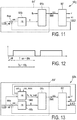
- Fig. 11 shows another embodiment of a driver device 50g including a first embodiment of the control unit 64' (the other parts of the driver device are schematically indicated by a single block 50').
- the LED current iLED is measured and compared to a (preset or variable) reference current iLED_ref in a comparison element 64a.
- the control error err_i is processed in a controller block 64b (indicated by PI) resulting in the duty cycle d as manipulating variable.
- a gate driving signals, representing the control signal S60 for the switching element 60 is formed in a (gate) driver block 64c.
- Fig. 12 shows a timing diagram for the (gate of the) the switching element 60.
- the duty cycle is basically related to the control error as typically done in a buck converter.
- a positive control error err_i causes an increase of d and vice versa.
- Self stabilizing behavior guarantees proper power balance without exceeding the limits of voltage stress across Cs. This is achieved by the proposed circuit arrangements as well as the control schemes adopted. If e.g. more power is drawn in average from the input than is taken from the output, the bus voltage vc will increase which in response will cause the control to decrease d, which in turn will reduce input power. In same manner the other embodiments can be operated, wherein the meaning of the duty cycle is toggled, i.e. d is to be replaced by 1-d for the embodiments of the driver device 50b, 50d, 50f compared to the embodiment of the driver device 50a, 50c, 50e. Other operation characteristics as the bus voltage and mains current (PF) are generally not explicitly controlled. They result from design and operation choices and tolerances.
- the maximum bus voltage is also explicitly controlled by means of the control, in particular by manipulating also the switching frequency. While still manipulating d to control the output current, fs is increased in response to an increasing bus voltage (as a result e.g. of a high mains voltage or a high output voltage). Alternatively, it is also possible to separately control T_on and T_off, which however will result in a similar switching pattern.
- the control enters a burst mode, i.e. switches off the converter periodically at a burst frequency below fs (e.g. 10 to 1000 times).
- fs can be used to shape the input current, either to improve the PF or to better comply with certain kinds of wall plug dimmers.
- FIG. 13 Still another embodiment of a driver device 50h including a second embodiment of the control unit 64" is depicted in Fig. 13 .
- the control unit 64" additionally comprises a second controller block 64d (indicated by PI) resulting in the switching frequency fs and fs_brst as manipulating variable provided to the (gate) driver block 64c.
- the second controller block 64d receives as input the reference current iLED_ref, the bus voltage vc, the input current ir, the input voltage vm and the maximum bus voltage vc_max.
- a driver device including a single-stage power converter topology with integrated preconditioner that feature high power factor while delivering constant output power to the load. Only a few components are required, among which half/full switch bridges and large electrolytic capacitors are avoided. This is achieved by properly controlling the power converter integrated with a low-power filter. Generally, only a single switch (e.g. a MOSFET transistor) is required to perform the conversion function.
- the resulting driver devices are preferably usable for off-line LED drivers employing high voltage LED strings.
- one boost inductor is operating in discontinuous conduction mode.
- a diode is preferably coupled in series (either that of the input rectifier bridge or a dedicated one).
- Two inductors are preferably used to filter out the high switching frequency current components.
- one high frequency decoupling capacitor is coupled at the output and, in some cases, a second one also at the input (i.e. output of the rectifier bridge).
- the switch node is further connected to a third inductor, in particular a high frequency inductor, which is connected in series to the small low frequency storage capacitor, thus forming a filter.
- the switch node is further connected to high frequency capacitor used as an intermediate storage element to transfer energy to the outputs within a switching cycle.
- the rectifier mains can be connected to either the boost inductor or to the switch.
- One terminal of the low frequency storage capacitor can be connected to either ground or to the load. Further, either only the load (e.g. LED) current is controlled constant (e.g. by duty cycle) or both LED current and bus voltage are controlled in two loops with manipulating the frequency, too.
- load e.g. LED
- LED current is controlled constant (e.g. by duty cycle) or both LED current and bus voltage are controlled in two loops with manipulating the frequency, too.
- the present invention is applied in consumer and "prosumer” (professional consumer) drivers, as LED drivers, above 2W, e.g. either integrated into a luminaire or external for HV LEDs. Further applications are non-mains isolated professional drivers with relaxed THD requirement (e.g. 20%) and HV LED string loads.
Landscapes
- Dc-Dc Converters (AREA)
- Circuit Arrangement For Electric Light Sources In General (AREA)
- Rectifiers (AREA)
Claims (15)
- Treibervorrichtung (50a-50f) zur Ansteuerung einer Last (22), insbesondere einer LED-Einheit mit einer oder mehreren LEDs (23), wobei die Treibervorrichtung umfasst:- Leistungseingangsanschlüsse (51, 52) zum Empfang einer gleichgerichteten Versorgungsspannung von einer externen Stromversorgung,- Leistungsausgangsanschlüsse (53, 54) zum Vorsehen einer Ansteuerspannung und/oder eines Stroms zur Ansteuerung einer Last (22),- eine mit den Leistungseingangsanschlüssen (51, 52) gekoppelte, einstufige Leistungsumwandlungseinheit (66a, 66b, 66c) mit einem einzelnen Schaltelement (60) und einem Energiespeicherelement (Ch), die beide mit einem Schaltknoten (55) gekoppelt sind, wobei die Leistungsausgangsanschlüsse (53, 54) durch den Ausgang der einstufigen Leistungsumwandlungseinheit dargestellt sind,- einen ersten Induktor (Lm), der zwischen dem Schaltknoten (55) und einem Leistungseingangsanschluss (51, 52) geschaltet ist,- eine Steuereinheit (58) zur Steuerung des Schaltelements (60),wobei- das Energiespeicherelement (Ch) zwischen dem Schaltknoten (55) und einem Zwischenknoten (58) geschaltet ist,- ein zweiter Induktor (Lo) zwischen dem Zwischenknoten (58) und einem Leistungsausgangsanschluss (53, 54) geschaltet ist, und- eine Diode (Do) zwischen dem Zwischenknoten (58) und einem Leistungsausgangsanschluss (53, 54) geschaltet ist,dadurch gekennzeichnet, dass- eine Filtereinheit (68) mit dem Schaltknoten (55) gekoppelt ist, wobei die Filtereinheit einen Filterinduktor (Lc) und einen Filterkondensator (Cs) umfasst.
- Treibervorrichtung (50a-50f) nach Anspruch 1,
wobei der Filterinduktor (Lc) und der Filterkondensator (Cs) in Reihe geschaltet sind, wobei ein Hochspannungsanschluss (56) der Filtereinheit mit dem Schaltknoten (55) gekoppelt ist. - Treibervorrichtung (50a, 50c, 50e) nach Anspruch 2,
wobei ein Niederspannungsanschluss (57) der Filtereinheit (68) mit einem Referenzpotential, insbesondere einem Erdpotential, gekoppelt ist, und/oder ein Leistungseingangsanschluss (52) mit einem Leistungsausgangsanschluss (53, 54) gekoppelt ist. - Treibervorrichtung (50b, 50d, 50f) nach Anspruch 2,
wobei ein Niederspannungsanschluss (57) der Filtereinheit (68) mit einem Leistungsausgangsanschluss (53, 54) gekoppelt ist, der nicht unmittelbar mit einem Leistungseingangsanschluss (51, 52) verbunden ist. - Treibervorrichtung (50a-50f) nach Anspruch 1,
wobei die einstufige Leistungsumwandlungseinheit einen Wandler vom Cuk-Typ (66a), vom SEPIC-Typ (66b) oder vom Zeta-Typ (66c) umfasst. - Treibervorrichtung (50a, 50b) nach Anspruch 1,
wobei- die einstufige Leistungsumwandlungseinheit (66a) einen Wandler vom Cuk-Typ umfasst,- das Schaltelement (60) zwischen dem Schaltknoten (55) und dem ersten Ausgangsanschluss (53) geschaltet ist,- der zweite Induktor (Lo) zwischen dem Zwischenknoten (58) und einem ersten Leistungsausgangsanschluss (54) geschaltet ist, und- die Diode (Do) zwischen dem Zwischenknoten (58) und einem zweiten Leistungsausgangsanschluss (53) geschaltet ist. - Treibervorrichtung (50c, 50d) nach Anspruch 1,
wobei- die einstufige Leistungsumwandlungseinheit (66b) einen Wandler vom SEPIC-Typ umfasst,- das Schaltelement (60) zwischen dem Schaltknoten (55) und dem ersten Ausgangsanschluss (54) geschaltet ist,- der zweite Induktor (Lo) zwischen dem Zwischenknoten (58) und einem zweiten Leistungsausgangsanschluss (54) geschaltet ist, und- die Diode (Do) zwischen dem Zwischenknoten (58) und einem ersten Leistungsausgangsanschluss (53) geschaltet ist. - Treibervorrichtung (50a-50d) nach Anspruch 6 oder 7,
wobei das Schaltelement (60) zwischen dem Schaltknoten (55) und einem zweiten Leistungseingangsanschluss (52) geschaltet ist. - Treibervorrichtung (50e-50f) nach Anspruch 1,
wobei- die einstufige Leistungsumwandlungseinheit (66c) einen Wandler vom Zeta-Typ umfasst,- das Schaltelement (60) zwischen einem ersten Leistungseingangsanschluss (51) und dem Schaltknoten (55) geschaltet ist,- eine erste Diode (Dm) in Reihe mit dem ersten Induktor (Lm) geschaltet ist,- der zweite Induktor (Lo) zwischen dem Zwischenknoten (58) und einem ersten Leistungsausgangsanschluss (53) geschaltet ist, und- die zweite Diode (Do) zwischen dem Zwischenknoten (58) und einem zweiten Leistungsausgangsanschluss (54) geschaltet ist. - Treibervorrichtung (50e, 50f) nach Anspruch 1,
die weiterhin einen Eingangsentkopplungskondensator (Cm) umfasst, der zwischen den Leistungseingangsanschlüssen (51, 52) geschaltet ist. - Treibervorrichtung (50a-50f) nach Anspruch 1,
die weiterhin einen Ausgangsentkopplungskondensator (Co) umfasst, der zwischen den Leistungsausgangsanschlüssen (53, 54) geschaltet ist. - Treibervorrichtung (50a-50f) nach Anspruch 1,
wobei ein zweiter Leistungseingangsanschluss (52) und ein zweiter Leistungsausgangsanschluss (53, 54) mit einem Referenzpotential verbunden sind. - Treibervorrichtung (50a-50f) nach Anspruch 1,
die weiterhin eine Gleichrichtereinheit (62) umfasst, um eine AC-Versorgungsspannung in die gleichgerichtete, periodische Versorgungsspannung gleichzurichten. - Treibervorrichtung (50a-50f) nach Anspruch 1,
wobei die Steuereinheit (64) so eingerichtet ist, dass sie den Ausgangsstrom konstant hält, um die Spannung über dem Energiespeicherelement unter einem vorher festgelegten Schwellenwert zu halten und/oder den Eingangsstrom zu formen. - Lichtvorrichtung, umfassend:- eine Lichtanordnung mit einer oder mehreren Lichteinheiten, insbesondere einer LED-Einheit (22) mit einer oder mehreren LEDs, sowie- eine Treibervorrichtung (50a-50f) zur Ansteuerung der Lichtanordnung nach einem der Ansprüche 1 bis 14.
Priority Applications (1)
| Application Number | Priority Date | Filing Date | Title |
|---|---|---|---|
| EP12732709.6A EP2721906B1 (de) | 2011-06-17 | 2012-06-11 | Einzelschalter-antriebsvorrichtung mit einem lc-filter zum antreiben einer last, insbesondere einer led-einheit |
Applications Claiming Priority (3)
| Application Number | Priority Date | Filing Date | Title |
|---|---|---|---|
| EP11170268 | 2011-06-17 | ||
| PCT/IB2012/052936 WO2012172472A1 (en) | 2011-06-17 | 2012-06-11 | Single switch driver device having lc filter, for driving a load, in particular an led unit |
| EP12732709.6A EP2721906B1 (de) | 2011-06-17 | 2012-06-11 | Einzelschalter-antriebsvorrichtung mit einem lc-filter zum antreiben einer last, insbesondere einer led-einheit |
Publications (2)
| Publication Number | Publication Date |
|---|---|
| EP2721906A1 EP2721906A1 (de) | 2014-04-23 |
| EP2721906B1 true EP2721906B1 (de) | 2017-08-16 |
Family
ID=46458569
Family Applications (1)
| Application Number | Title | Priority Date | Filing Date |
|---|---|---|---|
| EP12732709.6A Active EP2721906B1 (de) | 2011-06-17 | 2012-06-11 | Einzelschalter-antriebsvorrichtung mit einem lc-filter zum antreiben einer last, insbesondere einer led-einheit |
Country Status (5)
| Country | Link |
|---|---|
| US (1) | US9210749B2 (de) |
| EP (1) | EP2721906B1 (de) |
| JP (1) | JP6133280B2 (de) |
| CN (1) | CN103609198B (de) |
| WO (1) | WO2012172472A1 (de) |
Families Citing this family (20)
| Publication number | Priority date | Publication date | Assignee | Title |
|---|---|---|---|---|
| DE102010041632A1 (de) * | 2010-09-29 | 2012-03-29 | Osram Gesellschaft mit beschränkter Haftung | Schaltungsanordnung zum Betreiben mindestens zweier Halbleiterlichtquellen |
| JP6127290B2 (ja) * | 2013-05-28 | 2017-05-17 | 国立研究開発法人宇宙航空研究開発機構 | コンバータと多段倍電圧整流回路を併用した均等化機能付充放電器 |
| EP3150025B1 (de) | 2014-05-30 | 2018-03-14 | Philips Lighting Holding B.V. | Treiber zum treiben einer last |
| JP6429148B2 (ja) | 2014-11-20 | 2018-11-28 | パナソニックIpマネジメント株式会社 | 点灯装置およびそれを用いた照明器具 |
| JP6270698B2 (ja) * | 2014-11-26 | 2018-01-31 | 新電元工業株式会社 | Ledドライバ装置 |
| US9723667B1 (en) * | 2015-04-09 | 2017-08-01 | Universal Lighting Technologies, Inc. | Output tuning and dimming interface for an LED driver |
| US9693411B1 (en) * | 2015-04-09 | 2017-06-27 | Universal Lighting Technologies, Inc. | LED driver configuration and dimming interface for dynamic adjustment of driver operating parameters |
| DE102015210710A1 (de) * | 2015-06-11 | 2016-12-15 | Tridonic Gmbh & Co Kg | Getaktete Sperrwandlerschaltung |
| FR3040839B1 (fr) * | 2015-09-04 | 2019-10-25 | Commissariat A L'energie Atomique Et Aux Energies Alternatives | Convertisseur electronique et systeme d'eclairage comprenant un tel convertisseur |
| US9769896B1 (en) | 2015-12-04 | 2017-09-19 | Universal Lighting Technologies, Inc. | LED driver with offline tuning interface using hot and neutral inputs |
| CN105792421B (zh) * | 2016-04-05 | 2017-08-08 | 江南大学 | 一种无桥式led驱动电源 |
| CN106413202B (zh) * | 2016-11-25 | 2018-03-16 | 哈尔滨工业大学 | 基于SEPIC与Flyback电路的原边控制LED驱动电路 |
| US10264641B1 (en) | 2017-07-05 | 2019-04-16 | Universal Lighting Technologies, Inc. | Lighting system and method for dynamically regulating driven current to an analog or digital dimming interface |
| US10595383B1 (en) | 2018-01-26 | 2020-03-17 | Universal Lighting Technologies, Inc. | Device and method for programming or configuring of NFC equipped LED driver |
| US10588205B1 (en) | 2018-01-26 | 2020-03-10 | Universal Lighting Technologies, Inc. | Isolated digital control device for LED driver using NFC technology |
| US10560993B1 (en) | 2018-03-08 | 2020-02-11 | Universal Lighting Technologies, Inc. | Dimming controller for LED driver and method of indirect power estimation |
| EP3895299B1 (de) * | 2018-12-28 | 2024-06-19 | Huawei Digital Power Technologies Co., Ltd. | Hybridleistungswandler und verfahren |
| TWI699969B (zh) * | 2019-10-24 | 2020-07-21 | 瑞昱半導體股份有限公司 | 濾波器以及運作方法 |
| CN114205954B (zh) * | 2021-12-30 | 2024-07-09 | 福州大学 | 改进Sepic-LED驱动电路的无电解电容控制方法 |
| EP4220925A1 (de) * | 2022-01-26 | 2023-08-02 | Tridonic GmbH & Co. KG | Schaltwandler |
Family Cites Families (14)
| Publication number | Priority date | Publication date | Assignee | Title |
|---|---|---|---|---|
| JPH0832160B2 (ja) * | 1990-01-31 | 1996-03-27 | 三菱電機株式会社 | パルス電源装置 |
| JPH05176532A (ja) * | 1991-09-25 | 1993-07-13 | Yamaha Corp | 電源回路 |
| US5442539A (en) * | 1992-10-02 | 1995-08-15 | California Institute Of Technology | CuK DC-to-DC switching converter with input current shaping for unity power factor operation |
| US5442534A (en) * | 1993-02-23 | 1995-08-15 | California Institute Of Technology | Isolated multiple output Cuk converter with primary input voltage regulation feedback loop decoupled from secondary load regulation loops |
| US20030066555A1 (en) | 2000-12-04 | 2003-04-10 | Hui Ron Shu Yuen | Maximum power tracking technique for solar panels |
| KR100497393B1 (ko) | 2003-06-20 | 2005-06-23 | 삼성전자주식회사 | 디스플레이 패널 구동 시스템의 고효율 전원 공급 장치 및그 설계 방법 |
| US7847783B2 (en) * | 2005-10-11 | 2010-12-07 | O2Micro International Limited | Controller circuitry for light emitting diodes |
| US7889519B2 (en) * | 2006-01-12 | 2011-02-15 | Massachusetts Institute Of Technology | Methods and apparatus for a resonant converter |
| JP5169039B2 (ja) * | 2007-06-29 | 2013-03-27 | Nec東芝スペースシステム株式会社 | Dc‐dcコンバータ |
| JP2009089564A (ja) * | 2007-10-03 | 2009-04-23 | Nec Toshiba Space Systems Ltd | Dc/dcコンバータ |
| EP2299569B1 (de) * | 2009-09-21 | 2014-07-16 | BIONIC Engineering 5D+ AG | Gleichspannungsschaltwandler und Gleichspannungsschaltwandlungsverfahren |
| JP5759668B2 (ja) * | 2009-10-02 | 2015-08-05 | Fdk株式会社 | 多直列led駆動回路 |
| CN101867289B (zh) | 2010-05-19 | 2012-05-30 | 杭州矽力杰半导体技术有限公司 | 具有恒压/恒流输出的开关电源及其控制方法 |
| TWI454041B (zh) * | 2011-12-06 | 2014-09-21 | Champion Elite Co Ltd | Piezoelectric resonant light emitting diode driving circuit |
-
2012
- 2012-06-11 WO PCT/IB2012/052936 patent/WO2012172472A1/en not_active Ceased
- 2012-06-11 US US14/125,787 patent/US9210749B2/en active Active
- 2012-06-11 EP EP12732709.6A patent/EP2721906B1/de active Active
- 2012-06-11 CN CN201280029663.5A patent/CN103609198B/zh active Active
- 2012-06-11 JP JP2014515319A patent/JP6133280B2/ja active Active
Non-Patent Citations (1)
| Title |
|---|
| None * |
Also Published As
| Publication number | Publication date |
|---|---|
| CN103609198A (zh) | 2014-02-26 |
| JP2014520366A (ja) | 2014-08-21 |
| JP6133280B2 (ja) | 2017-05-24 |
| WO2012172472A1 (en) | 2012-12-20 |
| CN103609198B (zh) | 2016-10-19 |
| EP2721906A1 (de) | 2014-04-23 |
| US9210749B2 (en) | 2015-12-08 |
| US20140117868A1 (en) | 2014-05-01 |
Similar Documents
| Publication | Publication Date | Title |
|---|---|---|
| EP2721906B1 (de) | Einzelschalter-antriebsvorrichtung mit einem lc-filter zum antreiben einer last, insbesondere einer led-einheit | |
| EP2721726B1 (de) | Dc-dc-treibervorrichtung mit eingangs- und ausgangsfiltern zum antreiben einer last, insbesondere einer led-einheit | |
| EP2719063B1 (de) | Dc-dc-treibervorrichtung mit eingangs- und ausgangsfiltern zum antreiben einer last, insbesondere einer led-einheit | |
| CN102474189B (zh) | 低成本电源电路和方法 | |
| Zhang et al. | A precise passive current balancing method for multioutput LED drivers | |
| US8884548B2 (en) | Power factor correction converter with current regulated output | |
| US8228001B2 (en) | Method and apparatus of driving LED and OLED devices | |
| EP3050400B1 (de) | Elektronischer resonanter und isolierter zeta-halbbrückenwandler samt steuerverfahren | |
| CN103718652B (zh) | 用于驱动负载特别是led单元的驱动器设备和驱动方法 | |
| US8130519B2 (en) | Led driver with low harmonic distortion of input AC current and methods of controlling the same | |
| WO2018122329A1 (en) | Ac-dc converter circuit arrangement and method for operating a respective ac-dc converter circuit arrangement | |
| Agrawal et al. | A review of different DC/DC converters for power quality improvement in LED lighting load | |
| EP2249470B1 (de) | Kapazitätsverringerungsverfahren für eine impulsaktivierte Vorrichtung und zugehörige Vorrichtungen | |
| Padmavathi et al. | A survey on efficient converter driver techniques for LED lighting applications | |
| KR101454158B1 (ko) | 전해 커패시터 없는 LED 구동용 전원장치와 이의 120Hz 리플 저감기법 | |
| US8519638B2 (en) | Electronic ballast for a high intesity discharge lamp | |
| Buso et al. | A triple output driver for line-fed HBLED LAMPS | |
| CN101145738A (zh) | 电源转接器以及使用该电源转接器的电源供应系统 |
Legal Events
| Date | Code | Title | Description |
|---|---|---|---|
| PUAI | Public reference made under article 153(3) epc to a published international application that has entered the european phase |
Free format text: ORIGINAL CODE: 0009012 |
|
| 17P | Request for examination filed |
Effective date: 20140117 |
|
| AK | Designated contracting states |
Kind code of ref document: A1 Designated state(s): AL AT BE BG CH CY CZ DE DK EE ES FI FR GB GR HR HU IE IS IT LI LT LU LV MC MK MT NL NO PL PT RO RS SE SI SK SM TR |
|
| DAX | Request for extension of the european patent (deleted) | ||
| RAP1 | Party data changed (applicant data changed or rights of an application transferred) |
Owner name: PHILIPS LIGHTING HOLDING B.V. |
|
| GRAP | Despatch of communication of intention to grant a patent |
Free format text: ORIGINAL CODE: EPIDOSNIGR1 |
|
| INTG | Intention to grant announced |
Effective date: 20170303 |
|
| GRAS | Grant fee paid |
Free format text: ORIGINAL CODE: EPIDOSNIGR3 |
|
| GRAA | (expected) grant |
Free format text: ORIGINAL CODE: 0009210 |
|
| RIN1 | Information on inventor provided before grant (corrected) |
Inventor name: ELFERICH, REINHOLD Inventor name: LOPEZ, TONI |
|
| AK | Designated contracting states |
Kind code of ref document: B1 Designated state(s): AL AT BE BG CH CY CZ DE DK EE ES FI FR GB GR HR HU IE IS IT LI LT LU LV MC MK MT NL NO PL PT RO RS SE SI SK SM TR |
|
| REG | Reference to a national code |
Ref country code: GB Ref legal event code: FG4D |
|
| REG | Reference to a national code |
Ref country code: CH Ref legal event code: EP |
|
| REG | Reference to a national code |
Ref country code: IE Ref legal event code: FG4D |
|
| REG | Reference to a national code |
Ref country code: AT Ref legal event code: REF Ref document number: 920244 Country of ref document: AT Kind code of ref document: T Effective date: 20170915 |
|
| REG | Reference to a national code |
Ref country code: DE Ref legal event code: R096 Ref document number: 602012035995 Country of ref document: DE |
|
| REG | Reference to a national code |
Ref country code: NL Ref legal event code: MP Effective date: 20170816 |
|
| REG | Reference to a national code |
Ref country code: LT Ref legal event code: MG4D |
|
| REG | Reference to a national code |
Ref country code: AT Ref legal event code: MK05 Ref document number: 920244 Country of ref document: AT Kind code of ref document: T Effective date: 20170816 |
|
| PG25 | Lapsed in a contracting state [announced via postgrant information from national office to epo] |
Ref country code: AT Free format text: LAPSE BECAUSE OF FAILURE TO SUBMIT A TRANSLATION OF THE DESCRIPTION OR TO PAY THE FEE WITHIN THE PRESCRIBED TIME-LIMIT Effective date: 20170816 Ref country code: SE Free format text: LAPSE BECAUSE OF FAILURE TO SUBMIT A TRANSLATION OF THE DESCRIPTION OR TO PAY THE FEE WITHIN THE PRESCRIBED TIME-LIMIT Effective date: 20170816 Ref country code: NL Free format text: LAPSE BECAUSE OF FAILURE TO SUBMIT A TRANSLATION OF THE DESCRIPTION OR TO PAY THE FEE WITHIN THE PRESCRIBED TIME-LIMIT Effective date: 20170816 Ref country code: FI Free format text: LAPSE BECAUSE OF FAILURE TO SUBMIT A TRANSLATION OF THE DESCRIPTION OR TO PAY THE FEE WITHIN THE PRESCRIBED TIME-LIMIT Effective date: 20170816 Ref country code: LT Free format text: LAPSE BECAUSE OF FAILURE TO SUBMIT A TRANSLATION OF THE DESCRIPTION OR TO PAY THE FEE WITHIN THE PRESCRIBED TIME-LIMIT Effective date: 20170816 Ref country code: NO Free format text: LAPSE BECAUSE OF FAILURE TO SUBMIT A TRANSLATION OF THE DESCRIPTION OR TO PAY THE FEE WITHIN THE PRESCRIBED TIME-LIMIT Effective date: 20171116 |
|
| PG25 | Lapsed in a contracting state [announced via postgrant information from national office to epo] |
Ref country code: ES Free format text: LAPSE BECAUSE OF FAILURE TO SUBMIT A TRANSLATION OF THE DESCRIPTION OR TO PAY THE FEE WITHIN THE PRESCRIBED TIME-LIMIT Effective date: 20170816 Ref country code: GR Free format text: LAPSE BECAUSE OF FAILURE TO SUBMIT A TRANSLATION OF THE DESCRIPTION OR TO PAY THE FEE WITHIN THE PRESCRIBED TIME-LIMIT Effective date: 20171117 Ref country code: PL Free format text: LAPSE BECAUSE OF FAILURE TO SUBMIT A TRANSLATION OF THE DESCRIPTION OR TO PAY THE FEE WITHIN THE PRESCRIBED TIME-LIMIT Effective date: 20170816 Ref country code: IS Free format text: LAPSE BECAUSE OF FAILURE TO SUBMIT A TRANSLATION OF THE DESCRIPTION OR TO PAY THE FEE WITHIN THE PRESCRIBED TIME-LIMIT Effective date: 20171216 Ref country code: BG Free format text: LAPSE BECAUSE OF FAILURE TO SUBMIT A TRANSLATION OF THE DESCRIPTION OR TO PAY THE FEE WITHIN THE PRESCRIBED TIME-LIMIT Effective date: 20171116 Ref country code: RS Free format text: LAPSE BECAUSE OF FAILURE TO SUBMIT A TRANSLATION OF THE DESCRIPTION OR TO PAY THE FEE WITHIN THE PRESCRIBED TIME-LIMIT Effective date: 20170816 Ref country code: LV Free format text: LAPSE BECAUSE OF FAILURE TO SUBMIT A TRANSLATION OF THE DESCRIPTION OR TO PAY THE FEE WITHIN THE PRESCRIBED TIME-LIMIT Effective date: 20170816 |
|
| PG25 | Lapsed in a contracting state [announced via postgrant information from national office to epo] |
Ref country code: CZ Free format text: LAPSE BECAUSE OF FAILURE TO SUBMIT A TRANSLATION OF THE DESCRIPTION OR TO PAY THE FEE WITHIN THE PRESCRIBED TIME-LIMIT Effective date: 20170816 Ref country code: DK Free format text: LAPSE BECAUSE OF FAILURE TO SUBMIT A TRANSLATION OF THE DESCRIPTION OR TO PAY THE FEE WITHIN THE PRESCRIBED TIME-LIMIT Effective date: 20170816 Ref country code: RO Free format text: LAPSE BECAUSE OF FAILURE TO SUBMIT A TRANSLATION OF THE DESCRIPTION OR TO PAY THE FEE WITHIN THE PRESCRIBED TIME-LIMIT Effective date: 20170816 |
|
| REG | Reference to a national code |
Ref country code: DE Ref legal event code: R097 Ref document number: 602012035995 Country of ref document: DE |
|
| PG25 | Lapsed in a contracting state [announced via postgrant information from national office to epo] |
Ref country code: SM Free format text: LAPSE BECAUSE OF FAILURE TO SUBMIT A TRANSLATION OF THE DESCRIPTION OR TO PAY THE FEE WITHIN THE PRESCRIBED TIME-LIMIT Effective date: 20170816 Ref country code: IT Free format text: LAPSE BECAUSE OF FAILURE TO SUBMIT A TRANSLATION OF THE DESCRIPTION OR TO PAY THE FEE WITHIN THE PRESCRIBED TIME-LIMIT Effective date: 20170816 Ref country code: EE Free format text: LAPSE BECAUSE OF FAILURE TO SUBMIT A TRANSLATION OF THE DESCRIPTION OR TO PAY THE FEE WITHIN THE PRESCRIBED TIME-LIMIT Effective date: 20170816 Ref country code: SK Free format text: LAPSE BECAUSE OF FAILURE TO SUBMIT A TRANSLATION OF THE DESCRIPTION OR TO PAY THE FEE WITHIN THE PRESCRIBED TIME-LIMIT Effective date: 20170816 |
|
| PLBE | No opposition filed within time limit |
Free format text: ORIGINAL CODE: 0009261 |
|
| STAA | Information on the status of an ep patent application or granted ep patent |
Free format text: STATUS: NO OPPOSITION FILED WITHIN TIME LIMIT |
|
| REG | Reference to a national code |
Ref country code: FR Ref legal event code: PLFP Year of fee payment: 7 |
|
| 26N | No opposition filed |
Effective date: 20180517 |
|
| PG25 | Lapsed in a contracting state [announced via postgrant information from national office to epo] |
Ref country code: SI Free format text: LAPSE BECAUSE OF FAILURE TO SUBMIT A TRANSLATION OF THE DESCRIPTION OR TO PAY THE FEE WITHIN THE PRESCRIBED TIME-LIMIT Effective date: 20170816 |
|
| REG | Reference to a national code |
Ref country code: CH Ref legal event code: PL |
|
| REG | Reference to a national code |
Ref country code: BE Ref legal event code: MM Effective date: 20180630 |
|
| REG | Reference to a national code |
Ref country code: IE Ref legal event code: MM4A |
|
| PG25 | Lapsed in a contracting state [announced via postgrant information from national office to epo] |
Ref country code: MC Free format text: LAPSE BECAUSE OF FAILURE TO SUBMIT A TRANSLATION OF THE DESCRIPTION OR TO PAY THE FEE WITHIN THE PRESCRIBED TIME-LIMIT Effective date: 20170816 Ref country code: LU Free format text: LAPSE BECAUSE OF NON-PAYMENT OF DUE FEES Effective date: 20180611 |
|
| PG25 | Lapsed in a contracting state [announced via postgrant information from national office to epo] |
Ref country code: IE Free format text: LAPSE BECAUSE OF NON-PAYMENT OF DUE FEES Effective date: 20180611 Ref country code: CH Free format text: LAPSE BECAUSE OF NON-PAYMENT OF DUE FEES Effective date: 20180630 Ref country code: LI Free format text: LAPSE BECAUSE OF NON-PAYMENT OF DUE FEES Effective date: 20180630 |
|
| PG25 | Lapsed in a contracting state [announced via postgrant information from national office to epo] |
Ref country code: BE Free format text: LAPSE BECAUSE OF NON-PAYMENT OF DUE FEES Effective date: 20180630 |
|
| REG | Reference to a national code |
Ref country code: DE Ref legal event code: R079 Ref document number: 602012035995 Country of ref document: DE Free format text: PREVIOUS MAIN CLASS: H05B0033080000 Ipc: H05B0045000000 |
|
| PG25 | Lapsed in a contracting state [announced via postgrant information from national office to epo] |
Ref country code: MT Free format text: LAPSE BECAUSE OF NON-PAYMENT OF DUE FEES Effective date: 20180611 |
|
| PG25 | Lapsed in a contracting state [announced via postgrant information from national office to epo] |
Ref country code: TR Free format text: LAPSE BECAUSE OF FAILURE TO SUBMIT A TRANSLATION OF THE DESCRIPTION OR TO PAY THE FEE WITHIN THE PRESCRIBED TIME-LIMIT Effective date: 20170816 |
|
| PG25 | Lapsed in a contracting state [announced via postgrant information from national office to epo] |
Ref country code: HU Free format text: LAPSE BECAUSE OF FAILURE TO SUBMIT A TRANSLATION OF THE DESCRIPTION OR TO PAY THE FEE WITHIN THE PRESCRIBED TIME-LIMIT; INVALID AB INITIO Effective date: 20120611 Ref country code: PT Free format text: LAPSE BECAUSE OF FAILURE TO SUBMIT A TRANSLATION OF THE DESCRIPTION OR TO PAY THE FEE WITHIN THE PRESCRIBED TIME-LIMIT Effective date: 20170816 |
|
| PG25 | Lapsed in a contracting state [announced via postgrant information from national office to epo] |
Ref country code: HR Free format text: LAPSE BECAUSE OF FAILURE TO SUBMIT A TRANSLATION OF THE DESCRIPTION OR TO PAY THE FEE WITHIN THE PRESCRIBED TIME-LIMIT Effective date: 20170816 Ref country code: CY Free format text: LAPSE BECAUSE OF FAILURE TO SUBMIT A TRANSLATION OF THE DESCRIPTION OR TO PAY THE FEE WITHIN THE PRESCRIBED TIME-LIMIT Effective date: 20170816 Ref country code: MK Free format text: LAPSE BECAUSE OF NON-PAYMENT OF DUE FEES Effective date: 20170816 |
|
| PG25 | Lapsed in a contracting state [announced via postgrant information from national office to epo] |
Ref country code: AL Free format text: LAPSE BECAUSE OF FAILURE TO SUBMIT A TRANSLATION OF THE DESCRIPTION OR TO PAY THE FEE WITHIN THE PRESCRIBED TIME-LIMIT Effective date: 20170816 |
|
| REG | Reference to a national code |
Ref country code: DE Ref legal event code: R081 Ref document number: 602012035995 Country of ref document: DE Owner name: SIGNIFY HOLDING B.V., NL Free format text: FORMER OWNER: PHILIPS LIGHTING HOLDING B.V., EINDHOVEN, NL |
|
| P01 | Opt-out of the competence of the unified patent court (upc) registered |
Effective date: 20230421 |
|
| PGFP | Annual fee paid to national office [announced via postgrant information from national office to epo] |
Ref country code: GB Payment date: 20250617 Year of fee payment: 14 |
|
| PGFP | Annual fee paid to national office [announced via postgrant information from national office to epo] |
Ref country code: FR Payment date: 20250624 Year of fee payment: 14 |
|
| PGFP | Annual fee paid to national office [announced via postgrant information from national office to epo] |
Ref country code: DE Payment date: 20250827 Year of fee payment: 14 |