EP2719063B1 - Dc-dc-treibervorrichtung mit eingangs- und ausgangsfiltern zum antreiben einer last, insbesondere einer led-einheit - Google Patents
Dc-dc-treibervorrichtung mit eingangs- und ausgangsfiltern zum antreiben einer last, insbesondere einer led-einheit Download PDFInfo
- Publication number
- EP2719063B1 EP2719063B1 EP12729734.9A EP12729734A EP2719063B1 EP 2719063 B1 EP2719063 B1 EP 2719063B1 EP 12729734 A EP12729734 A EP 12729734A EP 2719063 B1 EP2719063 B1 EP 2719063B1
- Authority
- EP
- European Patent Office
- Prior art keywords
- unit
- voltage
- driver device
- coupled
- load
- Prior art date
- Legal status (The legal status is an assumption and is not a legal conclusion. Google has not performed a legal analysis and makes no representation as to the accuracy of the status listed.)
- Active
Links
- 238000004146 energy storage Methods 0.000 claims description 23
- 230000000737 periodic effect Effects 0.000 claims description 4
- 239000003990 capacitor Substances 0.000 description 39
- 238000010586 diagram Methods 0.000 description 17
- 238000006243 chemical reaction Methods 0.000 description 9
- 238000000034 method Methods 0.000 description 6
- 230000001360 synchronised effect Effects 0.000 description 6
- 230000002457 bidirectional effect Effects 0.000 description 4
- 230000008901 benefit Effects 0.000 description 3
- 230000001276 controlling effect Effects 0.000 description 3
- 230000001419 dependent effect Effects 0.000 description 3
- 241001672648 Vieira Species 0.000 description 1
- 230000009172 bursting Effects 0.000 description 1
- 230000008878 coupling Effects 0.000 description 1
- 238000010168 coupling process Methods 0.000 description 1
- 238000005859 coupling reaction Methods 0.000 description 1
- 238000001914 filtration Methods 0.000 description 1
- 238000002955 isolation Methods 0.000 description 1
- 239000013641 positive control Substances 0.000 description 1
- 230000001105 regulatory effect Effects 0.000 description 1
- 230000004044 response Effects 0.000 description 1
- 238000007493 shaping process Methods 0.000 description 1
- 230000007704 transition Effects 0.000 description 1
Images


Classifications
-
- H—ELECTRICITY
- H05—ELECTRIC TECHNIQUES NOT OTHERWISE PROVIDED FOR
- H05B—ELECTRIC HEATING; ELECTRIC LIGHT SOURCES NOT OTHERWISE PROVIDED FOR; CIRCUIT ARRANGEMENTS FOR ELECTRIC LIGHT SOURCES, IN GENERAL
- H05B45/00—Circuit arrangements for operating light-emitting diodes [LED]
- H05B45/30—Driver circuits
- H05B45/37—Converter circuits
- H05B45/3725—Switched mode power supply [SMPS]
- H05B45/38—Switched mode power supply [SMPS] using boost topology
-
- H—ELECTRICITY
- H02—GENERATION; CONVERSION OR DISTRIBUTION OF ELECTRIC POWER
- H02M—APPARATUS FOR CONVERSION BETWEEN AC AND AC, BETWEEN AC AND DC, OR BETWEEN DC AND DC, AND FOR USE WITH MAINS OR SIMILAR POWER SUPPLY SYSTEMS; CONVERSION OF DC OR AC INPUT POWER INTO SURGE OUTPUT POWER; CONTROL OR REGULATION THEREOF
- H02M3/00—Conversion of dc power input into dc power output
- H02M3/02—Conversion of dc power input into dc power output without intermediate conversion into ac
- H02M3/04—Conversion of dc power input into dc power output without intermediate conversion into ac by static converters
- H02M3/10—Conversion of dc power input into dc power output without intermediate conversion into ac by static converters using discharge tubes with control electrode or semiconductor devices with control electrode
- H02M3/145—Conversion of dc power input into dc power output without intermediate conversion into ac by static converters using discharge tubes with control electrode or semiconductor devices with control electrode using devices of a triode or transistor type requiring continuous application of a control signal
- H02M3/155—Conversion of dc power input into dc power output without intermediate conversion into ac by static converters using discharge tubes with control electrode or semiconductor devices with control electrode using devices of a triode or transistor type requiring continuous application of a control signal using semiconductor devices only
- H02M3/156—Conversion of dc power input into dc power output without intermediate conversion into ac by static converters using discharge tubes with control electrode or semiconductor devices with control electrode using devices of a triode or transistor type requiring continuous application of a control signal using semiconductor devices only with automatic control of output voltage or current, e.g. switching regulators
- H02M3/158—Conversion of dc power input into dc power output without intermediate conversion into ac by static converters using discharge tubes with control electrode or semiconductor devices with control electrode using devices of a triode or transistor type requiring continuous application of a control signal using semiconductor devices only with automatic control of output voltage or current, e.g. switching regulators including plural semiconductor devices as final control devices for a single load
- H02M3/1582—Buck-boost converters
-
- H—ELECTRICITY
- H05—ELECTRIC TECHNIQUES NOT OTHERWISE PROVIDED FOR
- H05B—ELECTRIC HEATING; ELECTRIC LIGHT SOURCES NOT OTHERWISE PROVIDED FOR; CIRCUIT ARRANGEMENTS FOR ELECTRIC LIGHT SOURCES, IN GENERAL
- H05B45/00—Circuit arrangements for operating light-emitting diodes [LED]
- H05B45/30—Driver circuits
- H05B45/37—Converter circuits
- H05B45/3725—Switched mode power supply [SMPS]
- H05B45/375—Switched mode power supply [SMPS] using buck topology
-
- H—ELECTRICITY
- H05—ELECTRIC TECHNIQUES NOT OTHERWISE PROVIDED FOR
- H05B—ELECTRIC HEATING; ELECTRIC LIGHT SOURCES NOT OTHERWISE PROVIDED FOR; CIRCUIT ARRANGEMENTS FOR ELECTRIC LIGHT SOURCES, IN GENERAL
- H05B45/00—Circuit arrangements for operating light-emitting diodes [LED]
- H05B45/30—Driver circuits
- H05B45/37—Converter circuits
- H05B45/3725—Switched mode power supply [SMPS]
- H05B45/39—Circuits containing inverter bridges
-
- H—ELECTRICITY
- H05—ELECTRIC TECHNIQUES NOT OTHERWISE PROVIDED FOR
- H05B—ELECTRIC HEATING; ELECTRIC LIGHT SOURCES NOT OTHERWISE PROVIDED FOR; CIRCUIT ARRANGEMENTS FOR ELECTRIC LIGHT SOURCES, IN GENERAL
- H05B45/00—Circuit arrangements for operating light-emitting diodes [LED]
- H05B45/10—Controlling the intensity of the light
-
- Y—GENERAL TAGGING OF NEW TECHNOLOGICAL DEVELOPMENTS; GENERAL TAGGING OF CROSS-SECTIONAL TECHNOLOGIES SPANNING OVER SEVERAL SECTIONS OF THE IPC; TECHNICAL SUBJECTS COVERED BY FORMER USPC CROSS-REFERENCE ART COLLECTIONS [XRACs] AND DIGESTS
- Y02—TECHNOLOGIES OR APPLICATIONS FOR MITIGATION OR ADAPTATION AGAINST CLIMATE CHANGE
- Y02B—CLIMATE CHANGE MITIGATION TECHNOLOGIES RELATED TO BUILDINGS, e.g. HOUSING, HOUSE APPLIANCES OR RELATED END-USER APPLICATIONS
- Y02B20/00—Energy efficient lighting technologies, e.g. halogen lamps or gas discharge lamps
- Y02B20/30—Semiconductor lamps, e.g. solid state lamps [SSL] light emitting diodes [LED] or organic LED [OLED]
Definitions
- the present invention relates to a driver device and a corresponding driving method for driving a load, in particular an LED unit comprising one or more LEDs. Further, the present invention relates to a light apparatus.
- a HPF converter for compact fluorescent lamps is described in " High-Power-Factor Electronic Ballast with Constant DC-Link Voltage", by Ricardo de Oliveira Brioschi and Jose Luiz F. Vieira, IEEE Transactions on Power Electronics, vol. 13, no. 6, 1998 .
- a half-bridge unit is shared by a boost converter and an LC parallel resonant converter, which is operated above resonance in order to obtain zero voltage switching (ZVS).
- ZVS zero voltage switching
- the bus voltage is controlled to be constant.
- Such a HPF converter typically requires a large bus capacitor and an output rectifier and has only narrow supply voltage and load (drive) voltage ranges.
- US2006/103363 discloses a DC-to-DC power regulator circuit.
- the circuit has input terminals for receiving a DC input voltage and having an output port for providing a regulated DC output voltage.
- the circuit comprises a boost input filter and a buck output filter comprising first respectively second inductor means. Between both filters a half bridge is provided.
- the circuit further includes an energy storage unit and a control unit. This circuit is only suitable for application within narrow supply and drive voltage ranges.
- the invention intends to provide a driver that may applied for broad supply and drive voltage ranges. Further, it is an object of the present invention to provide a corresponding light apparatus.
- a driver device comprising:
- a corresponding driving method is provided.
- a light apparatus comprising a light assembly having one or more light units, in particular an LED unit comprising one or more LEDs, and a driver device for driving said light assembly as provided according to the present invention.
- the present invention is based on the idea to integrate an offline synchronous boost converter into a synchronous buck converter.
- a load e.g. a HV LED unit
- a HF filter capacitor i.e. a mains filter
- the present invention provides both a constant drive current and power factors of 0.9 or higher.
- the separate capacitor voltage level (i.e. the level of the voltage across the power storage unit, which is preferably a capacitor; also called “bus capacitor” hereinafter) allows minimizing the stored energy.
- the buck current provides for lossless switching of both switching elements (preferably transistors, e.g. MOSFETS, said switching elements forming a half-bridge unit), which means high efficiency even at high frequencies, which allows for miniaturized inductors.
- a large bus capacitor can be dispensed with by allowing the bus voltage (i.e. the voltage across the energy storage unit) to vary during the supply cycle or a mains voltage cycle (e.g. by 20 to 80%) while keeping the output (drive) current constant.
- the output rectifier is omitted because the LC stage is replaced by a step down converter stage (i.e. a buck converter).
- narrow supply and drive voltage ranges can be overcome by a variation of the circuit and by dedicated half-bridge control. This makes it possible to design the invention for US mains and for European mains, while stil keeping the voltage stress of the half-bridge unit and energy storage element (e.g. storage capacitor) within typical limits.
- boost integrated synchronous buck converter BBB
- All of them can be controlled over full load range down to virtually zero load current by means of manipulating the duty cycle only or the switching frequency or by burst mode operation.
- the supply voltage may be a rectified periodic supply voltage provided by a power supply.
- a rectifier unit is preferably used (as part of the driver device or as an external unit coupled to the power input terminals) for rectifying the provided AC input voltage, e.g. a mains voltage, to the (rectified periodic) supply voltage.
- a rectifier unit may, for instance, comprise a generally known half-bridge or full-bridge rectifier.
- the supply voltage thus has the same polarity for either polarity of the AC input voltage.
- rectified periodic supply voltage is already provided at the power input terminals, e.g. from a rectifier (representing said external power supply) provided elsewhere, no further, or only general, elements (like e.g. an amplifier) are coupled to the power input terminals for shaping the provided supply voltage.
- the output side of the boost input filter unit can be coupled to the first or the second switching element of the half-bridge unit.
- the output terminals of the boost input filter unit are toggled, i.e. differently coupled to the half-bridge unit
- the input terminals of the buck output filter unit are also toggled, i.e. differently coupled to the half-bridge unit, in order to ensure self-stabilizing operation.
- either the load i.e. the power output terminals
- the energy storage unit e.g. a bus capacitor
- the load i.e. the power output terminals
- the energy storage unit e.g. a bus capacitor
- the various embodiments are provided for use in different applications and at different voltages, and are directed towards achieving certain aims. Often, a trade-off has to be made to select the optimum embodiment.
- the switching elements together form a half-bridge unit (also called switching unit, or sometimes called half-bridge).
- the switching elements can be implemented in various ways, e.g. including transistors (e.g. MOSFETs) or other controlled switching means.
- the energy storage unit comprises a charge capacitor, preferably a single capacitor.
- a second power input terminal and a second power output terminal are connected to a reference potential, in particular ground potential.
- the first power input terminal and the first power output terminal are directly connected, while the second power input terminal and a second power output are not directly connected.
- control unit is adapted for keeping the output current constant in order to keep the voltage across the energy storage element below a predetermined threshold and/or to shape the input current.
- Zero voltage switching of the switching elements is provided for by the design (components) of the proposed driver device.
- the tasks of the control are to keep the output current constant, possibly according to a reference current (set point), to keep the bus voltage (i.e. the voltage across the energy storage element) below a preset limit and/or to shape the input current.
- Said driver device 10 comprises a rectifier unit 12, a first-stage preconditioning unit 14 coupled to the output of the rectifier unit 12, a second-stage conversion unit 16 coupled to the output of the first-stage preconditioning unit 14 and a charge capacitor 18 coupled to the node 15 between said first-stage preconditioning unit 14 and said second-stage conversion unit 16.
- the rectifier unit 12 preferably comprises a rectifier, such as a known full-wave or half-wave bridge rectifier, for rectifying a provided AC input voltage V20, e.g., from an external mains voltage supply 20, to a rectified voltage V12.
- the load 22 is, in this embodiment, an LED unit comprising two LEDs 23 coupled to the output of the second stage conversion unit 16 whose output signal, in particular its drive voltage V16 and its drive current 116, is used to drive the load 22.
- the first-stage preconditioning unit 14 preconditions the rectified voltage V12 to an intermediate DC voltage V14, and the second-stage conversion unit 16 converts said intermediate DC voltage V14 to the desired DC drive voltage V16.
- the charge capacitor 18 is provided to store a charge, i.e. it is charged from the intermediate DC voltage V14, thereby filtering the low-frequency signal of the rectified voltage V12 to ensure a substantially constant output power of the second stage conversion unit 16, in particular a constant drive current 116 through the load 22.
- these elements 14, 16, 18 are generally known and widely used in such driver devices 10, they will not be described in more detail here.
- the driver device 10 complies with the aforementioned demand for a high power factor and low flicker at the expense of both larger space requirements and higher costs, which might be drastically limited however particularly in retrofit applications.
- the size of the first-stage preconditioning unit 14 may be mainly determined by the associated passive components, particularly if it comprises a switched mode power supply (SMPS), e.g. a boost converter, operating at a low or moderate switching frequency. Any attempt to increase the switching frequency so as to reduce the size of these filter components may yield a rapid increase in energy losses in the hard-switched SMPS and hence the need for larger heat sinks.
- SMPS switched mode power supply
- Embodiments of known single-stage driver devices 30a, 30b are schematically shown in Fig. 2a and Fig. 2b .
- Said driver device 30 comprises a rectifier unit 32 (that may be identical to the rectifier unit 12 of the two-stage driver device 10 shown in Fig. 1 ) and a conversion unit 34 (e.g. flyback converter for the embodiment shown in Fig. 2b or a buck converter for the embodiment shown in Fig. 2a ) coupled to the output of the rectifier unit 32.
- a charge capacitor 36a (representing a low-frequency input storage capacitor) is coupled to the node 33 between said rectifier unit 32 and said conversion unit 34.
- the charge capacitor 36b (representing a low-frequency output storage capacitor) is coupled to the node 35 between said conversion unit 34 and the load 22.
- the rectifier unit rectifies an AC input voltage V20, provided, e.g., from an external mains voltage supply (also called power supply) 20, to a rectified voltage V32.
- the rectified voltage V32 is converted into the desired DC drive voltage V34 for driving the load 22.
- the storage capacitors 18 (in Fig. 1 ) and 36a, 36b (in Figs. 2a , 2b ) are mainly provided to filter out the low-frequency component of the rectified voltage V12 in order to allow for a constant current into the load. Such capacitors are therefore large, particularly when placed in parallel with the load and when such a load is an LED.
- Figs. 1 and 2 are, for instance, described in Robert Erickson and Michael Madigan, "Design of a simple high-power-factor rectifier based on the flyback converter", IEEE Proceedings of the Applied Power Electronics Conferences and Expositions, 1990, pp. 792-801 .
- single-stage driver devices 30a,b although featuring a lower number of hardware components compared to two-stage driver devices as exemplarily shown in Fig. 1 , generally cannot offer a high power factor and a low perceptible flicker simultaneously due to limitations in the size of the charge capacitor, which must filter out the low-frequency component of the AC input voltage.
- single-stage driver devices may critically compromise size, lifetime and maximum-temperature operation of the load (e.g. a lamp) due to the use of large storage capacitors to mitigate perceptible flicker.
- Figs. 3 to 5 depict several embodiments of three different basic configurations of a driver device according to the present invention. These three configurations (embodiments of configuration 1 being shown in Fig. 3 , embodiments of configuration 2 being shown in Fig. 4 , embodiments of configuration 3 being shown in Fig. 5 ) differ in operation in terms of the in- and output voltage ranges which they support, as well as in terms of component stress at peak voltages and RMS currents. All three configurations show self-stabilizing behaviour, which allows controlling the output current so as to be constant at a predetermined bus voltage (i.e. the voltage vbus) ripple as will be explained below.
- the boost inductor i.e.
- the first inductor L1 of the boost input filter unit 71 is designed for operation in the discontinuous conduction mode. Further, ZVS is possible for both transitions of the switching elements (i.e. the switching elements 60, 61 forming a half-bridge unit), which is determined by the buck inductor (i.e. the second inductor L2 of the buck output filter unit 72).
- the diagrams shown in Figs. 6 to 11 refer to the three configurations shown in Figs. 3 , 4 and 5 . They all show a power factor of about 0.95 and a load of 10W.
- the output (drive) current io is composed of a DC component iLED through the LED string plus a HF current flowing through a parallel HF capacitor (not shown here; indicated as C_HF in Fig. 14b ).
- the LED current is kept constant by manipulating the duty cycle.
- a first embodiment of a driver device 50a according to the present invention is schematically shown in Fig. 3a . It comprises power input terminals 51, 52 for receiving a rectified supply voltage vm from an external power supply 20 (e.g. a mains voltage supply), which is preferably rectified by a rectifier 62.
- the driver device 50a further comprises power output terminals 53, 54 for providing a drive voltage vo and/or a drive current io for driving a load 22.
- a half-bridge unit 70 (also called switching unit or half-bridge) comprising a first 60 and a second 61 switching element is coupled in series between a high-voltage node 57 and a low-voltage node 58 and forms a switch node 59 between said first and said second switching element 60, 61.
- a boost input filter unit 71 comprising a first inductor L1 is coupled between said power input terminals 51, 52 and said half-bridge unit 70.
- a buck output filter unit 72 comprising a second inductor L2 is coupled between said half-bridge unit 70 and a power output terminal 53, 54.
- the input terminals 55a, 55b of the boost input filter unit 71 are coupled to the power input terminals 51, 52.
- the output terminals 55c, 55d of the boost input filter unit 71 are coupled to the switch node 59 and the low-voltage node 58 of the half-bridge unit 70.
- the input terminals 56a, 56b of the buck output filter unit 72 are coupled to the low-voltage node 58 and the switch node 59 of the half-bridge unit 70.
- the output terminals 56c, 56d of the buck output filter unit 72 are coupled to an energy storage unit 73, which is preferably a single bus capacitor C_bus.
- the power output terminals 53, 54, between which the load 22 is coupled, are directly coupled to the high-voltage node 57 and the low-voltage node 58 of the half-bridge unit 70.
- control unit 64 (implemented e.g. as a controller, processor or computer that is appropriately designed or programmed) is provided for controlling said switching elements 60, 61.
- a second embodiment of a driver device 50b according to the present invention is schematically shown in Fig. 3b .
- the output terminals 55c, 55d of the boost input filter unit 71 are coupled to the high-voltage node 57 and the switch node 59 of the half-bridge unit 70.
- the input terminals 56a, 56b of the buck output filter unit 72 are coupled to the switch node 57 and the high-voltage node 57 of the half-bridge unit 70.
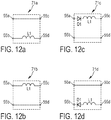
- Fig. 12 shows four embodiments of the boost input filter unit 71.
- a single first inductor L1 is provided, either in the connection from the first input terminal 55a to the first output terminal 55c or in the connection between the second input terminal 55b and the second output terminal 55d.
- a diode D1 is coupled in series to the first inductor L1.
- Fig. 13 shows two embodiments of the buck output filter unit 72.
- the second inductor L1 is provided in the connection from the first input terminal 56a to the first output terminal 56c
- the second inductor L2 is provided in the connection between the second input terminal 56b and the second output terminal 56d.
- the various embodiments of the boost input filter unit 71 shown in Fig. 12 and the various embodiments of the buck output filter unit 72 shown in Fig.13 can be coupled into the various embodiments of the driver unit as shown in Fig. 3 (and also into the embodiments shown in Figs. 4 and 5 ) instead of the respective embodiments of the boost input filter unit 71 of the buck output filter unit 72 shown in those figures.
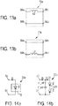
- Fig. 14a shows a single LED 23 as load 22a
- Fig. 14b shows a load 22b formed by a series coupling of several LEDs 23 coupled in parallel to a HF capacitor C_HF.
- the load current io is split into the capacitor current iC_HF and the LED current iLED.
- the diode D1 is used if an input HF filter capacitor (i.e. a mains filter) is connected at the boost input terminals 55a, 55b, i.e. between the power input terminals 51, 52.
- the diode D1 is omitted if a HF filter capacitor is connected at the AC input of rectifier 20 and if fast enough rectifiers are used therein. Except for the above restriction (i.e. the D1 is omitted), a HF capacitor may be connected to each of the three terminals, namely the power input terminals 51, 52, the boost input filter output terminals 55c, 55d, and the buck output filter output terminals 56c, 56d.
- the boost converter formed essentially by the first inductor L1 and the two switching elements 60, 61, supplies the load 22.
- the boost converter's current iLED (which corresponds to the output current io in the case of a load as shown in Fig. 14a ) can be kept constant throughout the mains cycle because part of the mains input current im is fed to the bus capacitor C_bus that is linked to the end of the buck converter, formed essentially by the switching elements 60, 61 and the second inductor L2, operating as a bidirectional converter, which supplies the load 22 at low mains input voltages.
- Signal iC_bus here LF bus cap current iC_bus in Fig. 6 , illustrates the bidirectional operation of the buck converter during a mains cycle ( Fig. 6 ) and how the buck converter supports ZVS at half-bridge turn off ( Fig.
- the duty cycle is indicated by means of d.
- a third embodiment of a driver device 50c according to the present invention is schematically shown in Fig. 4a .
- This embodiment is substantially identical to the embodiment of the driver device 50a, with the exception that in this embodiment the output terminals 55c, 55d of the boost input filter unit 71 are coupled to the low-voltage node 58 and switch node 59 of the half-bridge unit 70.
- the input terminals 56a, 56b of the buck output filter unit 72 are coupled to the switch node 59 and the high-voltage node 57 of the half-bridge unit 70.
- the energy storage unit 73 is coupled between the high-voltage node 57 and the low-voltage node 58 of the half-bridge unit 70.
- the power output terminals 53, 54, and thus also the load 22, are directly coupled to output terminals 56c, 56d of said buck output filter unit 72.
- a fourth embodiment of a driver device 50d according to the present invention is schematically shown in Fig. 4b .
- the output terminals 55c, 55d of the boost input filter unit 71 are coupled to the high-voltage node 57 and the switch node 59 of the half-bridge unit 70.
- the input terminals 56a, 56b of the buck output filter unit 72 are coupled to the switch node 57 and the low-voltage node 58 of the half-bridge unit 70.
- Figs. 4c and 4d show a fifth and a sixth embodiment of the driver device 50e, 50f.
- the embodiment shown in Fig. 4c is identical to the embodiment shown in Fig. 4b , but an additional diode D1 is provided in series to the first inductor L1.
- the diode D1 and the first inductor L1 are provided in the connection between the first input terminal 55a and the first output terminal 55c.
- the boost converter supplies the bus capacitor C_bus.
- the buck converter supplies the load 22.
- the buck converter is inverted with respect to the boost converter. Again, the load current iLED can be kept constant throughout the mains cycle because part of the mains input current im is fed to bus capacitor C_bus that supplies the load 22 at low mains input voltages.
- Signal iC_bus illustrates the bidirectional operation of the boost converter during a mains cycle ( Fig. 7 ) and again how the buck converter supports ZVS at turn off (signal io in Fig. 8 ).
- a seventh embodiment of a driver device 50g according to the present invention is schematically shown in Fig. 5a .
- This embodiment is substantially identical to the embodiment of the driver device 50c, but in this embodiment the energy storage unit 73 is coupled in series with the load 22, i.e. between the power output terminal 54 and the low-voltage terminal 58 of the half-bridge unit 70.
- FIG. 5b An eighth embodiment of a driver device 50h according to the present invention is schematically shown in Fig. 5b .
- the load 22 and the energy storage unit 70 are exchanged, i.e. the load 22 is coupled between the power output terminal 54 and the low-voltage terminal 58 of the half-bridge unit 70 and the energy storage unit 70 is coupled between the high-voltage terminal 57 of the half-bridge unit 70 and the power output terminal 53.
- the bus capacitor C_bus and the LED string 22 are stacked.
- the LED string 22 is connected to the switching element opposite to the one the boost converter is connected to.
- the load current iLED can be kept constant throughout the mains cycle because part of the mains input power is fed to the bus capacitor that supplies the load at low mains input voltages.
- Signal iC_bus illustrates the bidirectional operation of the boost converter during a mains cycle ( Fig. 10 ) and again how the buck converter 11 supports ZVS at half-bridge turn off (signal io in Fig. 7 ).
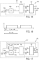
- Fig. 15 shows another embodiment of a driver device 50i including a first embodiment of the control unit 64' (the other parts of the driver device are schematically indicated by a single block 50').
- the LED current iLED (which is the DC component of output current io; cf. Fig. 14b ) is measured and compared to a (preset or variable) reference current iLED_ref in a comparison element 64a.
- the control error err i is processed in a controller block 64b (indicated by PI) resulting in the duty cycle d as manipulating variable.
- gate driving signals representing the control signals S60, S61 for both switching elements 60, 61, are formed in a (gate) driver block 64c.
- Fig. 16 shows a timing diagram for the (gate of the) the switching element 60.
- the duty cycle is basically related to the control error as typically generated in a buck converter.
- a positive control error err_i causes an increase of d and vice versa.
- Self-stabilizing behavior is achieved by the arrangement of the boost input filter unit with respect to the terminals of the buck output filter unit. If e.g. on average more power is drawn from the input than from the output, the bus voltage will increase, which will cause the control to decrease d, which in turn will reduce the input power.
- the other embodiments can be operated, wherein the meaning of the duty cycle is toggled, i.e. d is to be replaced by 1-d for the embodiments of the driver device 50b, 50d, 50e, 50f, 50h compared to the embodiment of the driver device 50a, 50c, 50g.
- Other operation characteristics such as the bus voltage and mains current (PF) are generally not explicitly controlled. They result from design and operation choices and tolerances.
- the maximum bus voltage is also explicitly controlled by means of the control, in particular by manipulating also the switching frequency. While d is still manipulated to control the output current, fs is increased in response to an increasing bus voltage (as a result e.g. of a high mains voltage or a high output voltage). Alternatively, it is also possible to separately control T_on and T_off, which however will result in a similar switching pattern.
- the control enters a burst mode, i.e. switches off the converter periodically at a burst frequency fs_brst below fs (e.g. 10 to 1000 times).
- fs can be used to shape the input current, either to improve the PF or to better comply with certain kinds of wall plug dimmers.
- a driver device 50j including a second embodiment of the control unit 64" is depicted in Fig. 17 .
- the control unit 64" additionally comprises a second controller block 64d (indicated by PI) resulting in the switching frequency fs and fs_brst as manipulating variable provided to the (gate) driver block 64c.
- the second controller block 64d receives as input the reference current iLED ref, the bus voltage vC_bus, the input current im, the input voltage vm and the maximum bus voltage vC_bus_max.
- a driver device and a corresponding method are proposed according to which an offline synchronous boost converter is integrated into a synchronous buck converter.
- the two ends are connected to a load, e.g. an HV LED load, and to a energy storage unit, e.g. a mains filter capacitor, which gives both constant LED current and power factors of 0.9 or higher.
- a load e.g. an HV LED load
- a energy storage unit e.g. a mains filter capacitor
- the separate capacitor voltage level allows minimizing the stored energy.
- the buck converter current provides for lossless half-bridge switching, which means high efficiency even at miniaturized inductors.
- BBB boost integrated synchronous buck converter
- the embodiments 50a, 50b of the driver device are mainly suited for load (LED string) voltages higher than peak supply voltage, e.g. for 120V mains supply and 250V LED strings.
- the embodiments 50c, 50d, 50e, 50f are mainly suited for load (LED string) voltages much lower than peak supply voltage, e.g. for 120V or 230V mains and LED string voltages of 10 to 150V. These embodiments show low root mean square (rms) currents in filters and half-bridge units.
- the embodiments 50g, 50h are mainly suited for applications like embodiments 50c-50f. These embodiments show reduced voltage stress on bus capacitors at somewhat increased rms currents in filters and half-bridge units.
- the advantage of the embodiments of the first type i.e. the embodiment 50a, 50c, 50g
- the supply voltage is ground referenced, which makes measuring vm and im a bit easier.
- the advantage of the embodiments of the second type i.e. the embodiments 50b, 50d, 50e, 50f, 50h
- the load is ground referenced, which sometimes helps measuring the current io and which might simplify isolation of possible heat sinks.
- a single ZVS half-bridge converter and two chokes i.e. a boost and a buck converter
- the switch node is preferably connected to rectified mains via a boost inductor.
- the two ends (of the buck and the boost converter) are connected to the load and the mains (bus) capacitor or a stack thereof.
- the buck converter is connected via the same switch as the boost converter.
- connections are altered. Either only the LED current is controlled so as to be constant (e.g. by duty cycle) or both the LED current and the bus voltage are controlled in two loops, causing the frequency to be manipulated too.
- the present invention is preferably applied in consumer and "prosumer” (professional consumer) drivers, in particular as LED drivers, above 2W, e.g. either integrated into a luminaire or arranged externally for HV LEDs. Further applications are non-mains isolated professional drivers with relaxed THD requirement (e.g. 20%) and HV LED string loads.
Landscapes
- Engineering & Computer Science (AREA)
- Power Engineering (AREA)
- Circuit Arrangement For Electric Light Sources In General (AREA)
- Dc-Dc Converters (AREA)
- Rectifiers (AREA)
Claims (13)
- Treibervorrichtung (50a-50j) zum Ansteuern einer Last (22), insbesondere einer LED-Einheit, welche eine oder mehrere LEDs (23) umfasst, wobei die Treibervorrichtung umfasst:- Stromversorgungseingangsanschlüsse (51, 52) zum Empfangen einer gleichgerichteten Versorgungsspannung aus einer externen Stromversorgung,- Stromversorgungsausgangsanschlüsse (53, 54) zum Bereitstellen einer Ansteuerspannung und/oder eines Ansteuerstroms zum Ansteuern einer Last (22),- eine Halbbrückeneinheit (70), umfassend ein erstes (60) und ein zweites (61) Schaltelement, welche zwischen einen Hochspannungsknoten (57) und einen Niederspannungsknoten (58) in Serie gekoppelt werden und einen Schaltknoten (59) zwischen dem ersten und dem zweiten Schaltelement aufweisen,- eine Boost-Eingabefiltereinheit (71), welche eine erste Induktivität (L1) umfasst, welche zwischen den Stromversorgungseingangsanschlüssen (51, 52) und der Halbbrückeneinheit (70) gekoppelt ist,- eine Buck-Ausgangsfiltereinheit (72), welche eine zweite Induktivität (L2) umfasst, welche zwischen der Halbbrückeneinheit (70) und zumindest einem der Stromversorgungsausgangsanschlüsse (53, 54) gekoppelt ist,- eine Energiespeichereinheit (73), und- eine Steuereinheit (64) zum Steuern der Schaltelemente (60, 61) dadurch gekennzeichnet, dass;i) die Stromversorgungsausgangsanschlüsse (53, 54) zum Bereitstellen einer Ansteuerspannung und/oder eines Ansteuerstroms zum Ansteuern einer Last (22) oder die Energiespeichereinheit (73) mit dem Hochspannungsknoten (57) und dem Niederspannungsknoten (58) der Halbbrückeneinheit (70) direkt gekoppelt sind, oder dass;ii) die Stromversorgungsausgangsanschlüsse (53, 54) zum Bereitstellen einer Ansteuerspannung und/oder eines Ansteuerstroms zum Ansteuern einer Last (22) und die Energiespeichereinheit (73) zwischen dem Hochspannungsknoten (57) und dem Niederspannungsknoten (58) der Halbbrückeneinheit (70) in Serie geschaltet sind.
- Treibervorrichtung (50a, 50c, 50g) nach Anspruch 1, wobei Ausgangsanschlüsse (55c, 55d) der Boost-Eingabefiltereinheit (71) an den Schaltknoten (59) und den Niederspannungsknoten (58) der Halbbrückeneinheit (70) gekoppelt sind.
- Treibervorrichtung (50a, 50c, 50g) nach Anspruch 2, wobei Eingangsanschlüsse (56a, 56b) der Buck-Ausgangsfiltereinheit (72) an den Hochspannungsknoten (57) und den Schaltknoten (59) der Halbbrückeneinheit (70) gekoppelt sind.
- Treibervorrichtung (50b, 50d, 50e, 50f, 50h) nach Anspruch 1, wobei Ausgangsanschlüsse (55c, 55d) der Boost-Eingabefiltereinheit (71) an den Hochspannungsknoten (57) und den Schaltknoten (59) der Halbbrückeneinheit (70) gekoppelt sind.
- Treibervorrichtung (50d, 50e, 50f, 50h) nach Anspruch 4, wobei Eingangsanschlüsse (56a, 56b) der Buck-Ausgangsfiltereinheit (72) an den Schaltknoten (59) und den Niederspannungsknoten (58) der Halbbrückeneinheit (70) gekoppelt sind.
- Treibervorrichtung (50a, 50b) nach Anspruch 1, wobei die Energiespeichereinheit (73) zwischen Ausgangsanschlüssen (56c, 56d) der Buck-Ausgangsfiltereinheit (72) gekoppelt ist.
- Treibervorrichtung (50c, 50d, 50e, 50f) nach Anspruch 1, wobei die Stromversorgungsausgangsanschlüsse (53, 54) an Ausgangsanschlüsse (56c, 56d) der Buck-Ausgangsfiltereinheit (72) direkt gekoppelt sind.
- Treibervorrichtung (50g, 50h) nach Anspruch 1, wobei die Energiespeichereinheit (73) zwischen dem Hochspannungsknoten (57) oder dem Niederspannungsknoten der Halbbrückeneinheit (70) und einem Ausgangsanschluss (56c, 56d) der Buck-Ausgangsfiltereinheit (72) gekoppelt ist.
- Treibervorrichtung (50g, 50h) nach Anspruch 8, wobei die Stromversorgungsausgangsanschlüsse (53, 54) an den Hochspannungsknoten (57) oder den Niederspannungsknoten der Halbbrückeneinheit (70) und einen Ausgangsanschluss (56c, 56d) der Buck-Ausgangsfiltereinheit (72) direkt gekoppelt sind.
- Treibervorrichtung (50a-50j) nach Anspruch 1, weiter eine Gleichrichtereinheit (62) zum Gleichrichten von einer Versorgungswechselspannung, insbesondere einer Netzspannung, auf die gleichgerichtete periodische Versorgungsspannung umfassend.
- Treibervorrichtung (50a-50j) nach Anspruch 1, wobei die Boost-Eingabefiltereinheit (71) eine Diode (D1) in Serie zu der ersten Induktivität (L1) umfasst.
- Treibervorrichtung (50a-50j) nach Anspruch 1, wobei die Steuereinheit (64) adaptiert ist, den Ausgangsstrom konstant zu halten, sodass die Spannung über das Energiespeicherelement hinweg unterhalb einer vorbestimmten Schwelle bleibt oder der Eingangsstrom geformt wird.
- Lichtvorrichtung, umfassend:- eine Lichtanordnung, umfassend eine oder mehrere Lichteinheiten, insbesondere eine LED-Einheit (22), umfassend eine oder mehrere LEDs, und- eine Treibervorrichtung (50a-50j) zum Ansteuern der Lichtanordnung nach einem der Ansprüche 1 bis 12.
Priority Applications (1)
| Application Number | Priority Date | Filing Date | Title |
|---|---|---|---|
| EP12729734.9A EP2719063B1 (de) | 2011-06-10 | 2012-06-04 | Dc-dc-treibervorrichtung mit eingangs- und ausgangsfiltern zum antreiben einer last, insbesondere einer led-einheit |
Applications Claiming Priority (3)
| Application Number | Priority Date | Filing Date | Title |
|---|---|---|---|
| EP11169523 | 2011-06-10 | ||
| EP12729734.9A EP2719063B1 (de) | 2011-06-10 | 2012-06-04 | Dc-dc-treibervorrichtung mit eingangs- und ausgangsfiltern zum antreiben einer last, insbesondere einer led-einheit |
| PCT/IB2012/052796 WO2012168847A1 (en) | 2011-06-10 | 2012-06-04 | Dc- dc driver device having input and output filters, for driving a load, in particular an led unit |
Publications (2)
| Publication Number | Publication Date |
|---|---|
| EP2719063A1 EP2719063A1 (de) | 2014-04-16 |
| EP2719063B1 true EP2719063B1 (de) | 2018-08-08 |
Family
ID=46354439
Family Applications (1)
| Application Number | Title | Priority Date | Filing Date |
|---|---|---|---|
| EP12729734.9A Active EP2719063B1 (de) | 2011-06-10 | 2012-06-04 | Dc-dc-treibervorrichtung mit eingangs- und ausgangsfiltern zum antreiben einer last, insbesondere einer led-einheit |
Country Status (7)
| Country | Link |
|---|---|
| US (1) | US9497814B2 (de) |
| EP (1) | EP2719063B1 (de) |
| JP (1) | JP6235464B2 (de) |
| CN (1) | CN103620934B (de) |
| BR (1) | BR112013031254A2 (de) |
| RU (1) | RU2587676C2 (de) |
| WO (1) | WO2012168847A1 (de) |
Families Citing this family (16)
| Publication number | Priority date | Publication date | Assignee | Title |
|---|---|---|---|---|
| US9544962B2 (en) | 2011-08-01 | 2017-01-10 | Philips Lighting Holding B.V. | Driver device and driving method for driving an LED unit |
| CN106465502B (zh) * | 2014-05-30 | 2018-10-12 | 飞利浦照明控股有限公司 | 用于驱动负载的驱动器 |
| EP2975767B1 (de) * | 2014-07-17 | 2020-01-22 | Nxp B.V. | Schaltnetzteil und Lichtstromkreis |
| US9973077B2 (en) | 2014-08-27 | 2018-05-15 | Schneider Electric It Corporation | Delta conversion rectifier |
| TWI548305B (zh) * | 2015-03-19 | 2016-09-01 | 喆富創新科技股份有限公司 | 發光二極體驅動電路 |
| US9685881B2 (en) * | 2015-06-04 | 2017-06-20 | Schneider Electric It Corporation | AC-DC rectifier system |
| DE102015122567A1 (de) * | 2015-12-22 | 2017-06-22 | NOVUM engineerING GmbH | Gleichstromwandler |
| CN108124341B (zh) * | 2016-11-30 | 2020-02-11 | 上海明石光电科技有限公司 | 一种led驱动器和led照明装置 |
| CN108347167B (zh) * | 2017-01-25 | 2021-07-13 | 通用电气公司 | 用于软切换dc—dc转换器的系统和方法 |
| KR101961412B1 (ko) * | 2017-03-15 | 2019-03-22 | 전북대학교산학협력단 | 3레벨 양방향 직류-직류 컨버터 |
| CN108307566B (zh) * | 2018-03-22 | 2023-11-24 | 深圳市博为光电股份有限公司 | 一种led光通信电源驱动系统 |
| US11063495B2 (en) | 2019-07-01 | 2021-07-13 | Nidec Motor Corporation | Heatsink clamp for multiple electronic components |
| AT522311B1 (de) * | 2019-07-02 | 2020-10-15 | Fachhochschule Technikum Wien | Hoch-Tiefsetzsteller mit großer Spannungsübersetzung |
| CN113796006A (zh) * | 2020-07-28 | 2021-12-14 | 深圳市大疆创新科技有限公司 | 驱动装置、芯片、拍摄装置和无人机 |
| TWI764403B (zh) * | 2020-12-02 | 2022-05-11 | 遠東科技大學 | 電壓轉換裝置 |
| US20230036095A1 (en) * | 2021-07-30 | 2023-02-02 | Texas Instruments Incorporated | Two-stage power supply architecture with flyback/llc and buck converter for led display |
Family Cites Families (18)
| Publication number | Priority date | Publication date | Assignee | Title |
|---|---|---|---|---|
| JPH09320776A (ja) * | 1996-05-28 | 1997-12-12 | Matsushita Electric Works Ltd | 放電灯点灯装置 |
| JP3692873B2 (ja) * | 1999-11-29 | 2005-09-07 | 松下電工株式会社 | 放電灯点灯装置 |
| DE20024002U1 (de) * | 2000-03-17 | 2009-03-26 | Tridonicatco Gmbh & Co. Kg | Spannungsversorgung von Leuchtdioden (LEDs) |
| US6278245B1 (en) * | 2000-03-30 | 2001-08-21 | Philips Electronics North America Corporation | Buck-boost function type electronic ballast with bus capacitor current sensing |
| US6198260B1 (en) | 2000-06-05 | 2001-03-06 | Technical Witts, Inc. | Zero voltage switching active reset power converters |
| RU2176847C1 (ru) * | 2000-10-17 | 2001-12-10 | Научно-производственная фирма "Уральские промышленные технологии" | Полумостовой автогенератор |
| US6577076B2 (en) * | 2001-09-04 | 2003-06-10 | Koninklijke Philips Electronics N.V. | Adaptive control for half-bridge universal lamp drivers |
| CN1315249C (zh) * | 2004-07-16 | 2007-05-09 | 王玉富 | 组合式直流-直流升压变换器 |
| US7202643B2 (en) * | 2004-11-12 | 2007-04-10 | Texas Instruments Incorporated | High efficiency DC-to-DC synchronous buck converter |
| KR101300007B1 (ko) | 2006-02-10 | 2013-08-27 | 필립스 솔리드-스테이트 라이팅 솔루션스, 인크. | 부하마다 단일 스위칭 스테이지를 사용하는 고역률 제어 전력 전달 방법 및 장치 |
| JP2008245388A (ja) * | 2007-03-27 | 2008-10-09 | Nec Computertechno Ltd | スイッチング電源装置 |
| EP2145381B1 (de) * | 2007-04-27 | 2016-04-06 | Koninklijke Philips N.V. | Selbstschwingender schalterstromkreis und treiberschaltung mit derartigem schalterstromkreis |
| WO2009040691A2 (en) | 2007-09-25 | 2009-04-02 | Nxp B.V. | Electronic power switching device |
| WO2009095836A2 (en) | 2008-01-29 | 2009-08-06 | Philips Intellectual Property & Standards Gmbh | Electronic driver circuit and method |
| JP5081110B2 (ja) | 2008-09-05 | 2012-11-21 | オリジン電気株式会社 | 昇圧形コンバータ |
| US8305064B2 (en) | 2008-12-24 | 2012-11-06 | Dora S.P.A. | Control device for a switching converter |
| US8686667B2 (en) * | 2010-01-26 | 2014-04-01 | Panasonic Corporation | Lighting power source with controlled charging operation for driving capacitor |
| CN102194648A (zh) * | 2010-02-24 | 2011-09-21 | 皇家飞利浦电子股份有限公司 | Hid照明系统 |
-
2012
- 2012-06-04 JP JP2014514187A patent/JP6235464B2/ja active Active
- 2012-06-04 RU RU2014100105/07A patent/RU2587676C2/ru active
- 2012-06-04 US US14/124,737 patent/US9497814B2/en active Active
- 2012-06-04 BR BR112013031254A patent/BR112013031254A2/pt not_active IP Right Cessation
- 2012-06-04 WO PCT/IB2012/052796 patent/WO2012168847A1/en active Application Filing
- 2012-06-04 EP EP12729734.9A patent/EP2719063B1/de active Active
- 2012-06-04 CN CN201280028346.1A patent/CN103620934B/zh active Active
Also Published As
| Publication number | Publication date |
|---|---|
| JP6235464B2 (ja) | 2017-11-22 |
| RU2014100105A (ru) | 2015-07-20 |
| CN103620934B (zh) | 2017-05-24 |
| BR112013031254A2 (pt) | 2017-04-25 |
| CN103620934A (zh) | 2014-03-05 |
| US9497814B2 (en) | 2016-11-15 |
| JP2014524102A (ja) | 2014-09-18 |
| US20140117867A1 (en) | 2014-05-01 |
| RU2587676C2 (ru) | 2016-06-20 |
| EP2719063A1 (de) | 2014-04-16 |
| WO2012168847A1 (en) | 2012-12-13 |
Similar Documents
| Publication | Publication Date | Title |
|---|---|---|
| EP2719063B1 (de) | Dc-dc-treibervorrichtung mit eingangs- und ausgangsfiltern zum antreiben einer last, insbesondere einer led-einheit | |
| EP2721726B1 (de) | Dc-dc-treibervorrichtung mit eingangs- und ausgangsfiltern zum antreiben einer last, insbesondere einer led-einheit | |
| US9210749B2 (en) | Single switch driver device having LC filter for driving an LED unit | |
| Lee et al. | A single-switch AC–DC LED driver based on a boost-flyback PFC converter with lossless snubber | |
| US9717120B2 (en) | Apparatus and methods of operation of passive LED lighting equipment | |
| JP3187637U (ja) | 非絶縁型ドライバ回路を使用した天井灯 | |
| US8482214B2 (en) | Apparatus and methods of operation of passive LED lighting equipment | |
| US20130119888A1 (en) | Power interface for a power supply circuit | |
| KR20120056162A (ko) | Led 구동장치 | |
| WO2008152565A2 (en) | Supply circuit, in particular for leds | |
| CN102348319A (zh) | 发光二极管灯驱动电源 | |
| EP2249470B1 (de) | Kapazitätsverringerungsverfahren für eine impulsaktivierte Vorrichtung und zugehörige Vorrichtungen | |
| US20110216567A1 (en) | Single switch inverter | |
| Lin et al. | A high efficiency integrated step-down Cuk and flyback converter for LED power driver | |
| US20100270931A1 (en) | Apparatus and methods of operation of passive led lighting equipment | |
| Mounika et al. | ADC controlled half-bridge LC series resonant converter for LED lighting | |
| KR101454158B1 (ko) | 전해 커패시터 없는 LED 구동용 전원장치와 이의 120Hz 리플 저감기법 | |
| Padmavathi et al. | A survey on efficient converter driver techniques for LED lighting applications | |
| KR20140049841A (ko) | Led 조명등용 전원 공급 장치 및 그 방법과 그를 이용한 led 조명 장치 | |
| US8519638B2 (en) | Electronic ballast for a high intesity discharge lamp | |
| Chang et al. | Driving circuit for high-brightness LED lamps | |
| TWI667941B (zh) | High-efficiency color LED lamp shared drive | |
| KR101700804B1 (ko) | 램프 구동용 전원 공급 장치 | |
| Buso et al. | A triple output driver for line-fed HBLED LAMPS |
Legal Events
| Date | Code | Title | Description |
|---|---|---|---|
| PUAI | Public reference made under article 153(3) epc to a published international application that has entered the european phase |
Free format text: ORIGINAL CODE: 0009012 |
|
| 17P | Request for examination filed |
Effective date: 20140110 |
|
| AK | Designated contracting states |
Kind code of ref document: A1 Designated state(s): AL AT BE BG CH CY CZ DE DK EE ES FI FR GB GR HR HU IE IS IT LI LT LU LV MC MK MT NL NO PL PT RO RS SE SI SK SM TR |
|
| DAX | Request for extension of the european patent (deleted) | ||
| RAP1 | Party data changed (applicant data changed or rights of an application transferred) |
Owner name: PHILIPS LIGHTING HOLDING B.V. |
|
| RIN1 | Information on inventor provided before grant (corrected) |
Inventor name: LOPEZ, TONI Inventor name: ELFERICH, REINHOLD |
|
| GRAP | Despatch of communication of intention to grant a patent |
Free format text: ORIGINAL CODE: EPIDOSNIGR1 |
|
| STAA | Information on the status of an ep patent application or granted ep patent |
Free format text: STATUS: GRANT OF PATENT IS INTENDED |
|
| INTG | Intention to grant announced |
Effective date: 20180207 |
|
| GRAS | Grant fee paid |
Free format text: ORIGINAL CODE: EPIDOSNIGR3 |
|
| GRAA | (expected) grant |
Free format text: ORIGINAL CODE: 0009210 |
|
| STAA | Information on the status of an ep patent application or granted ep patent |
Free format text: STATUS: THE PATENT HAS BEEN GRANTED |
|
| AK | Designated contracting states |
Kind code of ref document: B1 Designated state(s): AL AT BE BG CH CY CZ DE DK EE ES FI FR GB GR HR HU IE IS IT LI LT LU LV MC MK MT NL NO PL PT RO RS SE SI SK SM TR |
|
| REG | Reference to a national code |
Ref country code: GB Ref legal event code: FG4D |
|
| REG | Reference to a national code |
Ref country code: CH Ref legal event code: EP Ref country code: AT Ref legal event code: REF Ref document number: 1028131 Country of ref document: AT Kind code of ref document: T Effective date: 20180815 |
|
| REG | Reference to a national code |
Ref country code: IE Ref legal event code: FG4D |
|
| REG | Reference to a national code |
Ref country code: DE Ref legal event code: R096 Ref document number: 602012049443 Country of ref document: DE |
|
| RAP2 | Party data changed (patent owner data changed or rights of a patent transferred) |
Owner name: PHILIPS LIGHTING HOLDING B.V. |
|
| REG | Reference to a national code |
Ref country code: NL Ref legal event code: MP Effective date: 20180808 |
|
| REG | Reference to a national code |
Ref country code: LT Ref legal event code: MG4D |
|
| REG | Reference to a national code |
Ref country code: AT Ref legal event code: MK05 Ref document number: 1028131 Country of ref document: AT Kind code of ref document: T Effective date: 20180808 |
|
| PG25 | Lapsed in a contracting state [announced via postgrant information from national office to epo] |
Ref country code: FI Free format text: LAPSE BECAUSE OF FAILURE TO SUBMIT A TRANSLATION OF THE DESCRIPTION OR TO PAY THE FEE WITHIN THE PRESCRIBED TIME-LIMIT Effective date: 20180808 Ref country code: LT Free format text: LAPSE BECAUSE OF FAILURE TO SUBMIT A TRANSLATION OF THE DESCRIPTION OR TO PAY THE FEE WITHIN THE PRESCRIBED TIME-LIMIT Effective date: 20180808 Ref country code: PL Free format text: LAPSE BECAUSE OF FAILURE TO SUBMIT A TRANSLATION OF THE DESCRIPTION OR TO PAY THE FEE WITHIN THE PRESCRIBED TIME-LIMIT Effective date: 20180808 Ref country code: SE Free format text: LAPSE BECAUSE OF FAILURE TO SUBMIT A TRANSLATION OF THE DESCRIPTION OR TO PAY THE FEE WITHIN THE PRESCRIBED TIME-LIMIT Effective date: 20180808 Ref country code: NO Free format text: LAPSE BECAUSE OF FAILURE TO SUBMIT A TRANSLATION OF THE DESCRIPTION OR TO PAY THE FEE WITHIN THE PRESCRIBED TIME-LIMIT Effective date: 20181108 Ref country code: BG Free format text: LAPSE BECAUSE OF FAILURE TO SUBMIT A TRANSLATION OF THE DESCRIPTION OR TO PAY THE FEE WITHIN THE PRESCRIBED TIME-LIMIT Effective date: 20181108 Ref country code: GR Free format text: LAPSE BECAUSE OF FAILURE TO SUBMIT A TRANSLATION OF THE DESCRIPTION OR TO PAY THE FEE WITHIN THE PRESCRIBED TIME-LIMIT Effective date: 20181109 Ref country code: RS Free format text: LAPSE BECAUSE OF FAILURE TO SUBMIT A TRANSLATION OF THE DESCRIPTION OR TO PAY THE FEE WITHIN THE PRESCRIBED TIME-LIMIT Effective date: 20180808 Ref country code: NL Free format text: LAPSE BECAUSE OF FAILURE TO SUBMIT A TRANSLATION OF THE DESCRIPTION OR TO PAY THE FEE WITHIN THE PRESCRIBED TIME-LIMIT Effective date: 20180808 Ref country code: IS Free format text: LAPSE BECAUSE OF FAILURE TO SUBMIT A TRANSLATION OF THE DESCRIPTION OR TO PAY THE FEE WITHIN THE PRESCRIBED TIME-LIMIT Effective date: 20181208 Ref country code: AT Free format text: LAPSE BECAUSE OF FAILURE TO SUBMIT A TRANSLATION OF THE DESCRIPTION OR TO PAY THE FEE WITHIN THE PRESCRIBED TIME-LIMIT Effective date: 20180808 |
|
| PG25 | Lapsed in a contracting state [announced via postgrant information from national office to epo] |
Ref country code: HR Free format text: LAPSE BECAUSE OF FAILURE TO SUBMIT A TRANSLATION OF THE DESCRIPTION OR TO PAY THE FEE WITHIN THE PRESCRIBED TIME-LIMIT Effective date: 20180808 Ref country code: LV Free format text: LAPSE BECAUSE OF FAILURE TO SUBMIT A TRANSLATION OF THE DESCRIPTION OR TO PAY THE FEE WITHIN THE PRESCRIBED TIME-LIMIT Effective date: 20180808 Ref country code: AL Free format text: LAPSE BECAUSE OF FAILURE TO SUBMIT A TRANSLATION OF THE DESCRIPTION OR TO PAY THE FEE WITHIN THE PRESCRIBED TIME-LIMIT Effective date: 20180808 |
|
| RAP2 | Party data changed (patent owner data changed or rights of a patent transferred) |
Owner name: SIGNIFY HOLDING B.V. |
|
| PG25 | Lapsed in a contracting state [announced via postgrant information from national office to epo] |
Ref country code: ES Free format text: LAPSE BECAUSE OF FAILURE TO SUBMIT A TRANSLATION OF THE DESCRIPTION OR TO PAY THE FEE WITHIN THE PRESCRIBED TIME-LIMIT Effective date: 20180808 Ref country code: RO Free format text: LAPSE BECAUSE OF FAILURE TO SUBMIT A TRANSLATION OF THE DESCRIPTION OR TO PAY THE FEE WITHIN THE PRESCRIBED TIME-LIMIT Effective date: 20180808 Ref country code: IT Free format text: LAPSE BECAUSE OF FAILURE TO SUBMIT A TRANSLATION OF THE DESCRIPTION OR TO PAY THE FEE WITHIN THE PRESCRIBED TIME-LIMIT Effective date: 20180808 Ref country code: CZ Free format text: LAPSE BECAUSE OF FAILURE TO SUBMIT A TRANSLATION OF THE DESCRIPTION OR TO PAY THE FEE WITHIN THE PRESCRIBED TIME-LIMIT Effective date: 20180808 Ref country code: EE Free format text: LAPSE BECAUSE OF FAILURE TO SUBMIT A TRANSLATION OF THE DESCRIPTION OR TO PAY THE FEE WITHIN THE PRESCRIBED TIME-LIMIT Effective date: 20180808 |
|
| REG | Reference to a national code |
Ref country code: DE Ref legal event code: R097 Ref document number: 602012049443 Country of ref document: DE |
|
| PG25 | Lapsed in a contracting state [announced via postgrant information from national office to epo] |
Ref country code: DK Free format text: LAPSE BECAUSE OF FAILURE TO SUBMIT A TRANSLATION OF THE DESCRIPTION OR TO PAY THE FEE WITHIN THE PRESCRIBED TIME-LIMIT Effective date: 20180808 Ref country code: SK Free format text: LAPSE BECAUSE OF FAILURE TO SUBMIT A TRANSLATION OF THE DESCRIPTION OR TO PAY THE FEE WITHIN THE PRESCRIBED TIME-LIMIT Effective date: 20180808 Ref country code: SM Free format text: LAPSE BECAUSE OF FAILURE TO SUBMIT A TRANSLATION OF THE DESCRIPTION OR TO PAY THE FEE WITHIN THE PRESCRIBED TIME-LIMIT Effective date: 20180808 |
|
| PLBE | No opposition filed within time limit |
Free format text: ORIGINAL CODE: 0009261 |
|
| STAA | Information on the status of an ep patent application or granted ep patent |
Free format text: STATUS: NO OPPOSITION FILED WITHIN TIME LIMIT |
|
| 26N | No opposition filed |
Effective date: 20190509 |
|
| PG25 | Lapsed in a contracting state [announced via postgrant information from national office to epo] |
Ref country code: SI Free format text: LAPSE BECAUSE OF FAILURE TO SUBMIT A TRANSLATION OF THE DESCRIPTION OR TO PAY THE FEE WITHIN THE PRESCRIBED TIME-LIMIT Effective date: 20180808 |
|
| PG25 | Lapsed in a contracting state [announced via postgrant information from national office to epo] |
Ref country code: MC Free format text: LAPSE BECAUSE OF FAILURE TO SUBMIT A TRANSLATION OF THE DESCRIPTION OR TO PAY THE FEE WITHIN THE PRESCRIBED TIME-LIMIT Effective date: 20180808 |
|
| REG | Reference to a national code |
Ref country code: CH Ref legal event code: PL |
|
| REG | Reference to a national code |
Ref country code: BE Ref legal event code: MM Effective date: 20190630 |
|
| PG25 | Lapsed in a contracting state [announced via postgrant information from national office to epo] |
Ref country code: TR Free format text: LAPSE BECAUSE OF FAILURE TO SUBMIT A TRANSLATION OF THE DESCRIPTION OR TO PAY THE FEE WITHIN THE PRESCRIBED TIME-LIMIT Effective date: 20180808 |
|
| PG25 | Lapsed in a contracting state [announced via postgrant information from national office to epo] |
Ref country code: IE Free format text: LAPSE BECAUSE OF NON-PAYMENT OF DUE FEES Effective date: 20190604 |
|
| PG25 | Lapsed in a contracting state [announced via postgrant information from national office to epo] |
Ref country code: LU Free format text: LAPSE BECAUSE OF NON-PAYMENT OF DUE FEES Effective date: 20190604 Ref country code: BE Free format text: LAPSE BECAUSE OF NON-PAYMENT OF DUE FEES Effective date: 20190630 Ref country code: CH Free format text: LAPSE BECAUSE OF NON-PAYMENT OF DUE FEES Effective date: 20190630 Ref country code: LI Free format text: LAPSE BECAUSE OF NON-PAYMENT OF DUE FEES Effective date: 20190630 |
|
| PG25 | Lapsed in a contracting state [announced via postgrant information from national office to epo] |
Ref country code: PT Free format text: LAPSE BECAUSE OF FAILURE TO SUBMIT A TRANSLATION OF THE DESCRIPTION OR TO PAY THE FEE WITHIN THE PRESCRIBED TIME-LIMIT Effective date: 20181208 |
|
| REG | Reference to a national code |
Ref country code: DE Ref legal event code: R081 Ref document number: 602012049443 Country of ref document: DE Owner name: SIGNIFY HOLDING B.V., NL Free format text: FORMER OWNER: PHILIPS LIGHTING HOLDING B.V., EINDHOVEN, NL |
|
| PG25 | Lapsed in a contracting state [announced via postgrant information from national office to epo] |
Ref country code: CY Free format text: LAPSE BECAUSE OF FAILURE TO SUBMIT A TRANSLATION OF THE DESCRIPTION OR TO PAY THE FEE WITHIN THE PRESCRIBED TIME-LIMIT Effective date: 20180808 |
|
| PG25 | Lapsed in a contracting state [announced via postgrant information from national office to epo] |
Ref country code: HU Free format text: LAPSE BECAUSE OF FAILURE TO SUBMIT A TRANSLATION OF THE DESCRIPTION OR TO PAY THE FEE WITHIN THE PRESCRIBED TIME-LIMIT; INVALID AB INITIO Effective date: 20120604 Ref country code: MT Free format text: LAPSE BECAUSE OF FAILURE TO SUBMIT A TRANSLATION OF THE DESCRIPTION OR TO PAY THE FEE WITHIN THE PRESCRIBED TIME-LIMIT Effective date: 20180808 |
|
| PG25 | Lapsed in a contracting state [announced via postgrant information from national office to epo] |
Ref country code: MK Free format text: LAPSE BECAUSE OF FAILURE TO SUBMIT A TRANSLATION OF THE DESCRIPTION OR TO PAY THE FEE WITHIN THE PRESCRIBED TIME-LIMIT Effective date: 20180808 |
|
| PGFP | Annual fee paid to national office [announced via postgrant information from national office to epo] |
Ref country code: DE Payment date: 20220628 Year of fee payment: 11 |
|
| P01 | Opt-out of the competence of the unified patent court (upc) registered |
Effective date: 20230421 |
|
| PGFP | Annual fee paid to national office [announced via postgrant information from national office to epo] |
Ref country code: FR Payment date: 20230622 Year of fee payment: 12 |
|
| PGFP | Annual fee paid to national office [announced via postgrant information from national office to epo] |
Ref country code: GB Payment date: 20230620 Year of fee payment: 12 |
|
| REG | Reference to a national code |
Ref country code: DE Ref legal event code: R119 Ref document number: 602012049443 Country of ref document: DE |
|
| PG25 | Lapsed in a contracting state [announced via postgrant information from national office to epo] |
Ref country code: DE Free format text: LAPSE BECAUSE OF NON-PAYMENT OF DUE FEES Effective date: 20240103 |