EP2717316A1 - Method for producing strained germanium fin structures - Google Patents
Method for producing strained germanium fin structures Download PDFInfo
- Publication number
- EP2717316A1 EP2717316A1 EP12187332.7A EP12187332A EP2717316A1 EP 2717316 A1 EP2717316 A1 EP 2717316A1 EP 12187332 A EP12187332 A EP 12187332A EP 2717316 A1 EP2717316 A1 EP 2717316A1
- Authority
- EP
- European Patent Office
- Prior art keywords
- sige
- structures
- areas
- trenches
- substrate
- Prior art date
- Legal status (The legal status is an assumption and is not a legal conclusion. Google has not performed a legal analysis and makes no representation as to the accuracy of the status listed.)
- Granted
Links
Images

Classifications
-
- H—ELECTRICITY
- H10—SEMICONDUCTOR DEVICES; ELECTRIC SOLID-STATE DEVICES NOT OTHERWISE PROVIDED FOR
- H10D—INORGANIC ELECTRIC SEMICONDUCTOR DEVICES
- H10D62/00—Semiconductor bodies, or regions thereof, of devices having potential barriers
- H10D62/80—Semiconductor bodies, or regions thereof, of devices having potential barriers characterised by the materials
- H10D62/83—Semiconductor bodies, or regions thereof, of devices having potential barriers characterised by the materials being Group IV materials, e.g. B-doped Si or undoped Ge
- H10D62/832—Semiconductor bodies, or regions thereof, of devices having potential barriers characterised by the materials being Group IV materials, e.g. B-doped Si or undoped Ge being Group IV materials comprising two or more elements, e.g. SiGe
-
- H—ELECTRICITY
- H10—SEMICONDUCTOR DEVICES; ELECTRIC SOLID-STATE DEVICES NOT OTHERWISE PROVIDED FOR
- H10D—INORGANIC ELECTRIC SEMICONDUCTOR DEVICES
- H10D30/00—Field-effect transistors [FET]
- H10D30/01—Manufacture or treatment
- H10D30/021—Manufacture or treatment of FETs having insulated gates [IGFET]
- H10D30/024—Manufacture or treatment of FETs having insulated gates [IGFET] of fin field-effect transistors [FinFET]
Definitions
- the present invention is related to the production of fin-shaped structures comprising strained Ge on a SiGe buffer, mainly for use as quantum well digital logic transistors.
- a known technique for depositing a SiGe layer in a narrow trench is referred to as Aspect Ratio Trapping (ART). This technique allows filling of narrow trenches, e.g. obtained by STI (Shallow Trench Isolation) on a silicon substrate, with a SiGe layer that does not show defects in the top part of the trenches.
- STI Shallow Trench Isolation
- the invention is related to a method as disclosed in the appended claims.
- the method of the invention provides a way of producing fin-structures comprising strained Ge on a SiGe buffer of less than 20nm in width, without the above-described limitation on the size of the fins.
- the present invention is related to a method for producing one or more semiconductor fin structures, in particular fins comprising a SiGe buffer portion and a strained Ge top portion.
- the strained Ge portion is formed by a step of oxidizing SiGe structures extending outwards from an insulation surface, said insulation surface being preferably formed by the top surface of STI oxide regions produced in a Si substrate.
- the SiGe structures may be grown in the Si substrate by Aspect Ratio Trapping, thereby obtaining a SiGe structure that is relaxed and essentially defect free in a top region.
- the oxidation step results in the formation of a Ge region and a SiO 2 layer covering the fin.
- the oxidation is continued until a pure strained Ge top portion is obtained on the SiGe base of the fins.
- the process can involve the oxidation of separate SiGe structures formed by overgrowth of SiGe into separate mushroom-shaped overgrowth portions.
- the SiGe structures are formed after a CMP step and the step of etching the oxide regions in between the structures.
- the SiGe structures are obtained by patterning a SiGe layer that is sufficiently thick so as to obtain relaxed and defect free SiGe in a top sublayer of said SiGe layer.
- the invention is thus in particular related to a method for producing one or more semiconductor fin structures comprising the steps of :
- said oxidation and condensation continue until substantially none of the second material remains in the top portion of the fins, whilst the first material in said top portion remains in a strained condition.
- the step of producing said one or more elongate structures comprises the steps of :
- the step of producing said one or more elongate structures comprises the steps of :
- the step of producing said one or more elongate structures comprises the steps of :
- Said two different semiconductor materials may be silicon and germanium, wherein said compound material is SiGe, said base portion is a SiGe portion and said top portion is a strained Ge portion.
- SiGe is defined as Si x Ge 1-x , with x higher than 0.2.
- Said substrate may be a silicon substrate.
- the method of the invention may further comprise the step of depositing a cap layer formed of the second semiconductor material on said one or more relaxed and defect free fin-shaped structures consisting of said alloy material, before subjecting said structures to said oxidation step.
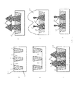
- Figure 1 illustrates a first embodiment of the method of the invention.
- Figure 2 illustrates a second embodiment of the method of the invention.
- Figures 1a to 1f illustrate a first embodiment of the method according to the invention.
- standard STI Shallow Trench Isolation
- SiGe 5 the semiconductor alloy Si x G 1-x , with x any suitable value known in the art for this type of alloy.
- the width and depth of the trenches 4 is such that aspect ratio trapping (ART) takes place, i.e. dislocations 6 become trapped by the sidewalls of the trenches 4.
- the result is a set of elongate SiGe structures 7, consisting of a base area 8 and a mushroom-shaped overgrowth area 9.
- the depth and aspect ratio of the trenches 4 is such that in said mushroom-shaped area 9 and in an upper portion 8' of the base area 8, relaxed and defect free SiGe is formed.
- a further etching step removes a portion of the STI oxide, resulting in part of the elongate SiGe structures 7 extending outwards with respect to oxide surface 10 (see figure 1d ).
- the mushroom-shaped portion 9 itself is the part that is extending outwards with respect to the oxide surface 14 (see figure 1c ). This structure is then subjected to a dry oxidation at high temperature, transforming the structures 7 into :
- the Ge top portion 17 is obtained by condensation of the Ge from the SiGe simultaneously with the oxidation of the Si.
- the oxidation step (hereafter also referred to as condensation/oxidation step) continues until the top portion 17 of the fins consists of substantially pure strained Ge, i.e. until no silicon is left in the top portion, whilst ensuring that the formed Ge is in a strained condition.
- the condensed volume is kept below the critical volume of plastic relaxation. This critical volume depends on the lattice mismatch between Ge and the initial relaxed SiGe, so mainly on the initial Ge concentration.
- the silicon oxide layer 18 is removed above the level 10 of the STI regions, by a suitable etching step, resulting in a set of fins 15 having a Ge top portion 17 of defect free strained Ge on a buffer of SiGe (the buffer being the base portion 16).
- silicon oxide formed in the oxidation step remains, i.e. in the preferred case where the regions 3 are also silicon oxide, the fins are embedded in a continuous oxide layer.
- a small over-etching may occur of the STI regions 3 during removal of the oxide 18, i.e. material removed from surface 10.
- the flanks of the base portions 16 may comprise a zone (not shown) of pure Ge or SiGe with higher Ge content, as Ge condensation may take place also in these regions.
- the fins 15 are suitable for producing quantum well FinFET transistors by applying further process steps as known in the art.
- the width of the top portions 17 can be lower than 20nm.
- the size of this top portion 17 can be designed by adequate choices in terms of the SiGe composition (value of x in Si x Ge 1-x ), the size of the overgrowth areas 9, the size of the trenches 4, taking into account the critical volume as stated above. Sufficient freedom is possible in the choice of these parameters to allow the production of very narrow fin structures starting from trenches 4 that are wide enough to ensure that no twin formation takes place during filling of the trench.
- the invention thus provides a solution for the above described problem : size reduction of the fins is possible without requiring trenches 4 that are too narrow to avoid twin formation in the upper part of the trench.
- the overgrowth of the SiGe is continued until a contiguous layer 20 of relaxed and defect free SiGe is obtained on top of the STI-substrate.
- the depth and aspect ratio of the trenches 4 is such that relaxed and defect free SiGe is obtained in the overgrowth area 20 and in an upper area 8' of the SiGe deposited in the trenches 4.
- CMP chemical-mechanical-polishing step
- An etch step follows to recess the STI oxide regions and form SiGe structures 7, a part of which is extending outwards from the STI surface 10. This structure is then subjected to the oxidation step as described above, again leading to the formation of :
- the strained Ge fins 15 are obtained, with remaining oxide areas 19 at the sides.
- a thin silicon cap layer is deposited (not shown), preferably by epitaxial growth, on top of the elongate structures 7, before performing the oxidation step.
- the purpose of this cap layer is to avoid oxidation of Germanium.
- the Si-cap forms a silicon oxide layer which will obstruct formation of germanium oxide, and ensure that all of the Ge moves to the center portion 17 by condensation.
- the oxidation of the cap may take place at a lower temperature than the oxidation of the SiGe.
- the invention is applicable also to materials other than Si and Ge.
- the condition is that the compound of the two materials is susceptible to a selective condensation/oxidation step, wherein one semiconductor is formed in a central portion of the fin by condensation, whereas the other oxidizes into a layer covering the fin.
- the oxide areas 3 may generally be referred to as 'insulation areas', so not necessarily formed of an oxide.
- diffusion anneal steps can be combined with condensation/oxidation steps in a cyclic process, in order to enhance the interdiffusion of the semiconductor elements in the alloy (e.g. Si and Ge).
- a condensation/oxidation and anneal cycles is to be regarded as an embodiment of the 'oxidation step' referred to in the claims.
- the structures 7 that are partly extending outwards with respect to the insulation areas 3 are obtained in another way than in the embodiments of figures 1 and 2 .
- a layer of SiGe is grown on a substrate, e.g. a Silicon substrate.
- the layer is grown at a sufficiently high thickness for un upper sublayer of the SiGe to be in a relaxed condition, and defect free.
- the thickness is sufficient so that dislocations caused by a mismatch between the SiGe and the underlying substrate do not propagate into said upper portion.
- the SiGe layer is few microns thick, preferably with a Ge gradient in order to bend dislocations defects forming in this way a graded strain relaxed buffer.
- a patterning and etching step is performed to produce trenches in the SiGe layer, whereafter said trenches are filled with an insulating material, for example silicon oxide. Possibly after a planarization step, this results in the same structure as the one shown in figure 2d , i.e. elongate areas of SiGe in between oxide areas 3, wherein a top portion 8' of the SiGe is relaxed and defect free.
- an insulating material for example silicon oxide
- the description of a layer being deposited or produced 'on' another layer or substrate includes the options of
Landscapes
- Insulated Gate Type Field-Effect Transistor (AREA)
- Element Separation (AREA)
- Crystals, And After-Treatments Of Crystals (AREA)
Abstract
Description
- The present invention is related to the production of fin-shaped structures comprising strained Ge on a SiGe buffer, mainly for use as quantum well digital logic transistors.
- In the search for high mobility materials in replacement of Si in digital logic structures, much interest has gone to the development of Ge channels, in particular strained Ge, due to the high carrier mobility characteristics of the material. In order to ensure optimum mobility, essentially defect-free Ge is required, which further leads to the need for a defect-free surface onto which the Ge is produced. A known technique for depositing a SiGe layer in a narrow trench is referred to as Aspect Ratio Trapping (ART). This technique allows filling of narrow trenches, e.g. obtained by STI (Shallow Trench Isolation) on a silicon substrate, with a SiGe layer that does not show defects in the top part of the trenches. All defects observed originate on the Si/SiGe interface and become trapped by the STI sidewalls. In 'Fabrication of Low-Defectivity, Compressively strained Ge on Si0.2Ge0.8 Structures using Aspect Ratio Trapping', J.-S. Park et al, Journal of the Electrochemical Society, 156(4)H249-H254 (2009), this technique is used and strained Ge layers are then grown on the thus obtained SiGe structures. Optimization of the quality of the Ge-layer is done by performing a pre-baking step prior to Ge-growth.
- A problem with the above-described technique wherein the strained Ge is obtained by epitaxial growth of Ge onto the SiGe in the trenches, is that when filling trenches with a width of less than 20nm, twin defects are formed at a higher level in the trench. This puts a limit on the production of fin structures in this way for fin-widths of less than 20nm.
- The invention is related to a method as disclosed in the appended claims. The method of the invention provides a way of producing fin-structures comprising strained Ge on a SiGe buffer of less than 20nm in width, without the above-described limitation on the size of the fins.
- The present invention is related to a method for producing one or more semiconductor fin structures, in particular fins comprising a SiGe buffer portion and a strained Ge top portion. The strained Ge portion is formed by a step of oxidizing SiGe structures extending outwards from an insulation surface, said insulation surface being preferably formed by the top surface of STI oxide regions produced in a Si substrate. The SiGe structures may be grown in the Si substrate by Aspect Ratio Trapping, thereby obtaining a SiGe structure that is relaxed and essentially defect free in a top region. The oxidation step results in the formation of a Ge region and a SiO2 layer covering the fin. The oxidation is continued until a pure strained Ge top portion is obtained on the SiGe base of the fins. The process can involve the oxidation of separate SiGe structures formed by overgrowth of SiGe into separate mushroom-shaped overgrowth portions. In another embodiment, the SiGe structures are formed after a CMP step and the step of etching the oxide regions in between the structures. According to a further embodiment, the SiGe structures are obtained by patterning a SiGe layer that is sufficiently thick so as to obtain relaxed and defect free SiGe in a top sublayer of said SiGe layer.
- The invention is thus in particular related to a method for producing one or more semiconductor fin structures comprising the steps of :
- Producing one or more elongate structures on a substrate, said structures consisting of an alloy of two different semiconductor materials, a part of said structures extending outwards with respect to the surface of an insulation layer present on said substrate, a top portion of said structures consisting of relaxed and defect free alloy material,
- subjecting said structure(s) to an oxidation step, so as to transform said structure(s) to :
- one or more fins comprising a base portion formed of said semiconductor alloy and a top portion formed of the first of said two semiconductor materials in a strained condition, said top portion being formed by condensation of said first material,
- a layer of oxide of the second of said two semiconductor materials, covering said fin(s), said oxide layer being formed by oxidation of said second material,
- removing the part of said layer of oxide of the second semiconductor material extending above said surface of said insulation layer, to thereby produce said one or more fin structures comprising a top portion of said first material in strained condition on a base portion of said alloy material.
- In the above method, said oxidation and condensation continue until substantially none of the second material remains in the top portion of the fins, whilst the first material in said top portion remains in a strained condition.
- According to an embodiment, the step of producing said one or more elongate structures comprises the steps of :
- Providing or producing a substrate having one or more fin-shaped areas on the surface, with insulation areas filling the spaces between said fin-shaped areas,
- Removing substrate material from said fin-shaped areas, thereby creating trenches between said insulation areas,
- Growing said semiconductor alloy in said trenches by a technique that allows Aspect Ratio Trapping of dislocations in said trenches, thereby obtaining relaxed and defect free semiconductor alloy material in an upper portion of said trenches, as well as in a mushroom-shaped portion overgrowing the upper edges of each of said trenches,
- Optionally, removing a top portion of said insulation areas, resulting in said mushroom-shaped portion and optionally at least part of said relaxed and defect free upper portion extending outwards with respect to the surface of said insulation areas or of the remainder of said insulation areas.
- According to another embodiment, the step of producing said one or more elongate structures comprises the steps of :
- Providing or producing a substrate having one or more fin-shaped areas on the surface, with insulation areas filling the spaces between said fin-shaped areas,
- Removing substrate material from said fin-shaped areas, thereby creating trenches between said insulation areas,
- Growing said semiconductor alloy in said trenches by a technique that allows Aspect Ratio Trapping of dislocations in said trenches, thereby obtaining relaxed and essentially defect free semiconductor alloy material in an upper portion of said trenches, as well as in a contiguous area overgrowing the upper edges of said trenches,
- Planarizing the substrate at least to the top level of said insulation areas,
- Removing a top portion of said insulation areas, resulting in at least part of said upper relaxed and defect free portion extending outwards with respect to the surface of the remainder of said insulation areas.
- According to still another embodiment, the step of producing said one or more elongate structures comprises the steps of :
- Producing a layer of said alloy on a substrate, said layer being sufficiently thick so that it comprises an upper area that is in a relaxed and defect free condition,
- Etching a plurality of trenches in said layer,
- Filling said trenches with an insulation material, optionally followed by a planarization step, to thereby obtain a substrate having one or more elongate areas of said alloy on the surface, with insulation areas filling the spaces between said elongate areas, thereby obtaining relaxed and essentially defect free semiconductor alloy material in an upper portion of said elongate areas,
- Removing a top portion of said insulation areas, resulting in at least part of said upper relaxed and defect free portion extending outwards with respect to the surface of the remainder of said insulation areas.
- Said two different semiconductor materials may be silicon and germanium, wherein said compound material is SiGe, said base portion is a SiGe portion and said top portion is a strained Ge portion.
- According to an embodiment, SiGe is defined as SixGe1-x, with x higher than 0.2. Said substrate may be a silicon substrate.
- The method of the invention may further comprise the step of depositing a cap layer formed of the second semiconductor material on said one or more relaxed and defect free fin-shaped structures consisting of said alloy material, before subjecting said structures to said oxidation step.
-
Figure 1 illustrates a first embodiment of the method of the invention. -
Figure 2 illustrates a second embodiment of the method of the invention. - Of a number of terms, the following definitions are valid within the present description as well as in the claims :
- When a volume of a semiconductor or semiconductor alloy, for example SiGe, is said to be 'relaxed' or in 'relaxed condition', this means that the lattice parameter of the material in the volume is equal to the standard equilibrium lattice parameter, in other words there is no strain effect from the substrate on which the volume is produced, having another lattice parameter (smaller in the case of SiGe grown on Si).
- When a volume of semiconductor or a semiconductor alloy is said to be 'strained', this means that said volume is formed of first crystalline material having a first lattice constant, and is overlying a second crystalline material having a second lattice constant different then the first, wherein the crystalline in-plane lattices are matched at the interface between the first and second material, i.e. the first lattice is stretched or compressed to match the second lattice, thereby inducing strain in the first crystalline material.
- A volume of a semiconductor or semiconductor alloy (e.g. Ge or SiGe) is said to be 'defect free' when there are essentially no defects appearing as a consequence of propagating dislocations in the volume.
-
Figures 1a to 1f illustrate a first embodiment of the method according to the invention. On asilicon substrate 1, standard STI (Shallow Trench Isolation) is performed to form silicon fin-shaped structures 2, separated byoxide regions 3, and planarized to alevel surface 14. The width of the fin-shaped structures at the top can be about 40nm for example. Then the finshaped structures 2 are fully or partially removed by an etching step, resulting in a set oftrenches 4. These trenches are filled by growing SiGe 5, preferably by the known technique referred to as RPCVD, Reduced Pressure Chemical Vapour Deposition. By 'SiGe' is meant in the present context : the semiconductor alloy SixG1-x, with x any suitable value known in the art for this type of alloy. Preferably, x is higher than 0.2, for example x=0.25. - The width and depth of the
trenches 4 is such that aspect ratio trapping (ART) takes place, i.e.dislocations 6 become trapped by the sidewalls of thetrenches 4. The result is a set ofelongate SiGe structures 7, consisting of abase area 8 and a mushroom-shapedovergrowth area 9. The depth and aspect ratio of thetrenches 4 is such that in said mushroom-shapedarea 9 and in an upper portion 8' of thebase area 8, relaxed and defect free SiGe is formed. Optionally, a further etching step removes a portion of the STI oxide, resulting in part of theelongate SiGe structures 7 extending outwards with respect to oxide surface 10 (seefigure 1d ). When this last etching step is not performed, the mushroom-shapedportion 9 itself is the part that is extending outwards with respect to the oxide surface 14 (seefigure 1c ). This structure is then subjected to a dry oxidation at high temperature, transforming thestructures 7 into : -
fins 15 comprising aSiGe base portion 16 and atop portion 17 of pure strained Ge formed by condensation of Ge, - a
layer 18 of silicon oxide covering saidfins 15, formed by oxidation of Si, - The Ge
top portion 17 is obtained by condensation of the Ge from the SiGe simultaneously with the oxidation of the Si. The oxidation step (hereafter also referred to as condensation/oxidation step) continues until thetop portion 17 of the fins consists of substantially pure strained Ge, i.e. until no silicon is left in the top portion, whilst ensuring that the formed Ge is in a strained condition. To ensure that the Ge is in a strained condition, the condensed volume is kept below the critical volume of plastic relaxation. This critical volume depends on the lattice mismatch between Ge and the initial relaxed SiGe, so mainly on the initial Ge concentration. - Then the
silicon oxide layer 18 is removed above thelevel 10 of the STI regions, by a suitable etching step, resulting in a set offins 15 having a Getop portion 17 of defect free strained Ge on a buffer of SiGe (the buffer being the base portion 16). In theregions 19 adjacent to the base portions of the fins, silicon oxide formed in the oxidation step remains, i.e. in the preferred case where theregions 3 are also silicon oxide, the fins are embedded in a continuous oxide layer. A small over-etching may occur of theSTI regions 3 during removal of theoxide 18, i.e. material removed fromsurface 10. The flanks of thebase portions 16 may comprise a zone (not shown) of pure Ge or SiGe with higher Ge content, as Ge condensation may take place also in these regions. - The
fins 15 are suitable for producing quantum well FinFET transistors by applying further process steps as known in the art. The width of thetop portions 17 can be lower than 20nm. The size of thistop portion 17 can be designed by adequate choices in terms of the SiGe composition (value of x in SixGe1-x), the size of theovergrowth areas 9, the size of thetrenches 4, taking into account the critical volume as stated above. Sufficient freedom is possible in the choice of these parameters to allow the production of very narrow fin structures starting fromtrenches 4 that are wide enough to ensure that no twin formation takes place during filling of the trench. The invention thus provides a solution for the above described problem : size reduction of the fins is possible without requiringtrenches 4 that are too narrow to avoid twin formation in the upper part of the trench. - In another embodiment illustrated in
figures 2a to 2g , the overgrowth of the SiGe is continued until acontiguous layer 20 of relaxed and defect free SiGe is obtained on top of the STI-substrate. As in the previous embodiment, the depth and aspect ratio of thetrenches 4 is such that relaxed and defect free SiGe is obtained in theovergrowth area 20 and in an upper area 8' of the SiGe deposited in thetrenches 4. This is followed by a chemical-mechanical-polishing step (CMP) to remove saidlayer 20 and planarize the substrate at least to thelevel 14 of the STI substrate, seefigure 2d ('at least' meaning that CMP could be continued to a level lower than level 14). An etch step follows to recess the STI oxide regions and formSiGe structures 7, a part of which is extending outwards from theSTI surface 10. This structure is then subjected to the oxidation step as described above, again leading to the formation of : -
fins 15 comprising aSiGe base area 16 and atop area 17 of pure strained Ge formed by condensation (taking into account again the critical volume as referred to above), - a
layer 18 of silicon oxide covering saidfins 15, formed by oxidation of Si. - After removal of the
silicon oxide 18, thestrained Ge fins 15 are obtained, with remainingoxide areas 19 at the sides. - According to an embodiment, a thin silicon cap layer is deposited (not shown), preferably by epitaxial growth, on top of the
elongate structures 7, before performing the oxidation step. The purpose of this cap layer is to avoid oxidation of Germanium. When the oxidation starts, the Si-cap forms a silicon oxide layer which will obstruct formation of germanium oxide, and ensure that all of the Ge moves to thecenter portion 17 by condensation. The oxidation of the cap may take place at a lower temperature than the oxidation of the SiGe. - The invention is applicable also to materials other than Si and Ge. The condition is that the compound of the two materials is susceptible to a selective condensation/oxidation step, wherein one semiconductor is formed in a central portion of the fin by condensation, whereas the other oxidizes into a layer covering the fin. The
oxide areas 3 may generally be referred to as 'insulation areas', so not necessarily formed of an oxide. - According to an embodiment, diffusion anneal steps can be combined with condensation/oxidation steps in a cyclic process, in order to enhance the interdiffusion of the semiconductor elements in the alloy (e.g. Si and Ge). This would mean subjecting the wafer to a condensation/oxidation, e.g. at 900°C, during a first timespan, then subjecting it to a diffusion anneal in an inert gas preferably at the same temperature during a second timespan, and repeating the condensation/oxidation and anneal during at least one additional series of a first and second timespans (not necessarily equal to the first series). Such a sequence of condensation/oxidation and anneal cycles is to be regarded as an embodiment of the 'oxidation step' referred to in the claims.
- According to another embodiment, the
structures 7 that are partly extending outwards with respect to theinsulation areas 3 are obtained in another way than in the embodiments offigures 1 and2 . This will again be explained for the case of Si and Ge, though it is applicable also to other materials. According to this embodiment, a layer of SiGe is grown on a substrate, e.g. a Silicon substrate. The layer is grown at a sufficiently high thickness for un upper sublayer of the SiGe to be in a relaxed condition, and defect free. In other words, the thickness is sufficient so that dislocations caused by a mismatch between the SiGe and the underlying substrate do not propagate into said upper portion. In the particular example of SiGe on Si, the SiGe layer is few microns thick, preferably with a Ge gradient in order to bend dislocations defects forming in this way a graded strain relaxed buffer. - Then a patterning and etching step is performed to produce trenches in the SiGe layer, whereafter said trenches are filled with an insulating material, for example silicon oxide. Possibly after a planarization step, this results in the same structure as the one shown in
figure 2d , i.e. elongate areas of SiGe in betweenoxide areas 3, wherein a top portion 8' of the SiGe is relaxed and defect free. The steps shown infigures 2e to 2g and described above in relation to these figures are then performed in the same way. - Starting from a Si-wafer having ∼40nm wide fin-shaped
Si areas 2 separated by silicon oxide STI regions 3: - 1)EPI :
- load wafer in the EPI tool,
- Si bake at 850°C to remove native oxide,
- Remove Si to a depth of ∼300nm at 850°C, by an HCl vapour etch performed in situ in the EPI chamber, to form
trenches 4 - grow SiGe by RPCVD at 20Torr in
trenches 4 until forming a mushroom-shaped overgrowth 9 (growing SiGe to a thickness of 400nm in total) at 550°C, - grow a 2nm Si cap at 600°C by RPCVD.
- 2) oxidation process performed in an oxidation furnace :
- Si cap is first oxidized at 700°C,
- the rest of the condensation/oxidation process is done afterwards at 900°C during a suitable timespan, ranging from minutes to hours, depending the how much has to be oxidized.
- removal of SiO2 by a wet etch such as an HF dip. Preferably a conformal etch is used, i.e. essentially the same thickness of oxide is removed everywhere, so that the oxide in
regions 19 remains in place.
- While the invention has been illustrated and described in detail in the drawings and foregoing description, such illustration and description are to be considered illustrative or exemplary and not restrictive. Other variations to the disclosed embodiments can be understood and effected by those skilled in the art in practicing the claimed invention, from a study of the drawings, the disclosure and the appended claims. In the claims, the word "comprising" does not exclude other elements or steps, and the indefinite article "a" or "an" does not exclude a plurality. The mere fact that certain measures are recited in mutually different dependent claims does not indicate that a combination of these measures cannot be used to advantage. Any reference signs in the claims should not be construed as limiting the scope.
- The foregoing description details certain embodiments of the invention. It will be appreciated, however, that no matter how detailed the foregoing appears in text, the invention may be practiced in many ways, and is therefore not limited to the embodiments disclosed. It should be noted that the use of particular terminology when describing certain features or aspects of the invention should not be taken to imply that the terminology is being re-defined herein to be restricted to include any specific characteristics of the features or aspects of the invention with which that terminology is associated.
- Unless specifically specified, the description of a layer being deposited or produced 'on' another layer or substrate, includes the options of
- said layer being produced or deposited directly on, i.e. in contact with, said other layer or substrate, and
- said layer being produced on one or a stack of intermediate layers between said layer and said other layer or substrate.
Claims (8)
- A method for producing one or more semiconductor fin structures (15) comprising the steps of :• Producing one or more elongate structures (7) on a substrate, said structures consisting of an alloy of two different semiconductor materials, a part of said structures extending outwards with respect to the surface (10,14) of an insulation layer present on said substrate, a top portion (8',9) of said structures consisting of relaxed and defect free alloy material,• subjecting said structure(s) (7) to an oxidation step, so as to transform said structure(s) to :• one or more fins (15) comprising a base portion (16) formed of said semiconductor alloy and a top portion (17) formed of the first of said two semiconductor materials in a strained condition, said top portion being formed by condensation of said first material,• a layer of oxide (18) of the second of said two semiconductor materials, covering said fin(s) (15), said oxide layer (18) being formed by oxidation of said second material,• removing the part of said layer (18) of oxide of the second semiconductor material extending above said surface (10,14) of said insulation layer, to thereby produce said one or more fin structures (15) comprising a top portion (17) of said first material in strained condition on a base portion (16) of said alloy material.
- Method according to claim 1, wherein the step of producing said one or more elongate structures (7) comprises the steps of :• Providing or producing a substrate (1) having one or more fin-shaped areas (2) on the surface, with insulation areas (3) filling the spaces between said fin-shaped areas,• Removing substrate material from said fin-shaped areas (2), thereby creating trenches (4) between said insulation areas (3),• Growing said semiconductor alloy in said trenches (4) by a technique that allows Aspect Ratio Trapping of dislocations in said trenches, thereby obtaining relaxed and defect free semiconductor alloy material in an upper portion (8') of said trenches, as well as in a mushroom-shaped portion (9) overgrowing the upper edges of each of said trenches (4),• Optionally, removing a top portion of said insulation areas (3), resulting in said mushroom-shaped portion (9) and optionally at least part of said relaxed and defect free upper portion (8') extending outwards with respect to the surface (14,10) of said insulation areas (3) or of the remainder of said insulation areas (3).
- Method according to claim 1, wherein the step of producing said one or more elongate structures (7) comprises the steps of :• Providing or producing a substrate (1) having one or more fin-shaped areas (2) on the surface, with insulation areas (3) filling the spaces between said fin-shaped areas,• Removing substrate material from said fin-shaped areas (2), thereby creating trenches (4) between said insulation areas (3),• Growing said semiconductor alloy in said trenches by a technique that allows Aspect Ratio Trapping of dislocations in said trenches, thereby obtaining relaxed and essentially defect free semiconductor alloy material in an upper portion (8') of said trenches, as well as in a contiguous area (20) overgrowing the upper edges of said trenches,• Planarizing the substrate at least to the top level (14) of said insulation areas (3),• Removing a top portion of said insulation areas (3), resulting in at least part of said upper relaxed and defect free portion (8') extending outwards with respect to the surface (10) of the remainder of said insulation areas (3).
- Method according to claim 1, wherein the step of producing said one or more elongate structures (7) comprises the steps of :• Producing a layer of said alloy on a substrate, said layer being sufficiently thick so that it comprises an upper area that is in a relaxed and defect free condition,• Etching a plurality of trenches in said layer,• Filling said trenches with an insulation material, optionally followed by a planarization step, to thereby obtain a substrate having one or more elongate areas of said alloy on the surface, with insulation areas (3) filling the spaces between said elongate areas, thereby obtaining relaxed and essentially defect free semiconductor alloy material in an upper portion (8') of said elongate areas,• Removing a top portion of said insulation areas (3), resulting in at least part of said upper relaxed and defect free portion (8') extending outwards with respect to the surface (10) of the remainder of said insulation areas (3).
- Method according to any one of claims 1 to 4, wherein said two different semiconductor materials are silicon and germanium, and wherein said compound material is SiGe, said base portion (16) is a SiGe portion and said top portion (17) is a strained Ge portion.
- Method according to claim 5, wherein SiGe is defined as SixGe1-x, with x higher than 0.2.
- Method according to any one of claims 1 to 6, wherein said substrate is a silicon substrate.
- Method according to any one of claims 1 to 7, further comprising the step of depositing a cap layer formed of the second semiconductor material on said one or more relaxed and defect free fin-shaped structures (7) consisting of said alloy material, before subjecting said structures to said oxidation step.
Priority Applications (3)
| Application Number | Priority Date | Filing Date | Title |
|---|---|---|---|
| EP12187332.7A EP2717316B1 (en) | 2012-10-05 | 2012-10-05 | Method for producing strained germanium fin structures |
| JP2013174538A JP6204749B2 (en) | 2012-10-05 | 2013-08-26 | Method for producing strained Ge fin structure |
| US14/047,950 US9263528B2 (en) | 2012-10-05 | 2013-10-07 | Method for producing strained Ge fin structures |
Applications Claiming Priority (1)
| Application Number | Priority Date | Filing Date | Title |
|---|---|---|---|
| EP12187332.7A EP2717316B1 (en) | 2012-10-05 | 2012-10-05 | Method for producing strained germanium fin structures |
Publications (2)
| Publication Number | Publication Date |
|---|---|
| EP2717316A1 true EP2717316A1 (en) | 2014-04-09 |
| EP2717316B1 EP2717316B1 (en) | 2019-08-14 |
Family
ID=47172280
Family Applications (1)
| Application Number | Title | Priority Date | Filing Date |
|---|---|---|---|
| EP12187332.7A Active EP2717316B1 (en) | 2012-10-05 | 2012-10-05 | Method for producing strained germanium fin structures |
Country Status (3)
| Country | Link |
|---|---|
| US (1) | US9263528B2 (en) |
| EP (1) | EP2717316B1 (en) |
| JP (1) | JP6204749B2 (en) |
Cited By (1)
| Publication number | Priority date | Publication date | Assignee | Title |
|---|---|---|---|---|
| CN106856191A (en) * | 2015-12-09 | 2017-06-16 | 中芯国际集成电路制造(上海)有限公司 | Semiconductor structure and forming method thereof |
Families Citing this family (20)
| Publication number | Priority date | Publication date | Assignee | Title |
|---|---|---|---|---|
| KR20130014861A (en) * | 2011-08-01 | 2013-02-12 | 삼성전자주식회사 | High electron mobility transistor and method of manufacturing the same |
| US9406530B2 (en) * | 2014-03-27 | 2016-08-02 | International Business Machines Corporation | Techniques for fabricating reduced-line-edge-roughness trenches for aspect ratio trapping |
| US9196479B1 (en) * | 2014-07-03 | 2015-11-24 | International Business Machines Corporation | Method of co-integration of strained silicon and strained germanium in semiconductor devices including fin structures |
| US9276117B1 (en) * | 2014-08-19 | 2016-03-01 | Taiwan Semiconductor Manufacturing Company, Ltd. | Structure and method and FinFET device |
| US10032912B2 (en) | 2014-12-31 | 2018-07-24 | Stmicroelectronics, Inc. | Semiconductor integrated structure having an epitaxial SiGe layer extending from silicon-containing regions formed between segments of oxide regions |
| KR102274750B1 (en) | 2015-01-27 | 2021-07-07 | 삼성전자주식회사 | Method for fabricating semiconductor device |
| US9754968B2 (en) | 2015-04-30 | 2017-09-05 | International Business Machines Corporation | Structure and method to form III-V, Ge and SiGe fins on insulator |
| US9548361B1 (en) * | 2015-06-30 | 2017-01-17 | Stmicroelectronics, Inc. | Method of using a sacrificial gate structure to make a metal gate FinFET transistor |
| US9330984B1 (en) | 2015-07-08 | 2016-05-03 | International Business Machines Corporation | CMOS fin integration on SOI substrate |
| US9418900B1 (en) | 2015-07-15 | 2016-08-16 | International Business Machines Corporation | Silicon germanium and silicon fins on oxide from bulk wafer |
| US9679899B2 (en) | 2015-08-24 | 2017-06-13 | Stmicroelectronics, Inc. | Co-integration of tensile silicon and compressive silicon germanium |
| US20170084616A1 (en) | 2015-09-18 | 2017-03-23 | Samsung Electronics Co., Ltd. | Semiconductor Devices Including FINFET Structures with Increased Gate Surface |
| US9378952B1 (en) | 2015-09-30 | 2016-06-28 | International Business Machines Corporation | Tall relaxed high percentage silicon germanium fins on insulator |
| US9570443B1 (en) | 2015-11-23 | 2017-02-14 | International Business Machines Corporation | Field effect transistor including strained germanium fins |
| US9659960B1 (en) * | 2015-12-09 | 2017-05-23 | International Business Machines Corporation | Extremely thin silicon-on-insulator silicon germanium device without edge strain relaxation |
| US9911660B2 (en) | 2016-04-26 | 2018-03-06 | Lam Research Corporation | Methods for forming germanium and silicon germanium nanowire devices |
| US10374089B2 (en) | 2017-12-22 | 2019-08-06 | International Business Machines Corporation | Tensile strain in NFET channel |
| US10424639B1 (en) * | 2018-04-19 | 2019-09-24 | International Business Machines Corporation | Nanosheet transistor with high-mobility channel |
| US11011517B2 (en) | 2019-01-02 | 2021-05-18 | International Business Machines Corporation | Semiconductor structure including first FinFET devices for low power applications and second FinFET devices for high power applications |
| CN109761189A (en) * | 2019-01-10 | 2019-05-17 | 中国科学院长春光学精密机械与物理研究所 | A kind of preparation method and application of polymer microfibers structure |
Citations (8)
| Publication number | Priority date | Publication date | Assignee | Title |
|---|---|---|---|---|
| DE102007007261A1 (en) * | 2006-02-15 | 2007-08-23 | Kabushiki Kaisha Toshiba | Semiconductor device has semiconductor layer and multiple side surfaces, where semiconductor layer section is vertical symmetric to given direction in vertical and horizontal directions and gate electrode is formed on gate insulated film |
| US20070221956A1 (en) * | 2006-03-23 | 2007-09-27 | Kabushiki Kaisha Toshiba | Semiconductor device and method of fabricating the same |
| WO2007112066A2 (en) * | 2006-03-24 | 2007-10-04 | Amberwave Systems Corporation | Lattice-mismatched semiconductor structures and related methods for device fabrication |
| WO2008039495A1 (en) * | 2006-09-27 | 2008-04-03 | Amberwave Systems Corporation | Tri-gate field-effect transistors formed by aspect ratio trapping |
| US20090085027A1 (en) * | 2007-09-29 | 2009-04-02 | Intel Corporation | Three dimensional strained quantum wells and three dimensional strained surface channels by ge confinement method |
| US20100025683A1 (en) * | 2008-07-01 | 2010-02-04 | Amberwave Systems Corporation | Reduction of edge effects from aspect ration trapping |
| US20110147811A1 (en) * | 2009-12-23 | 2011-06-23 | Kavalieros Jack T | Two-dimensional condensation for uniaxially strained semiconductor fins |
| US20110180847A1 (en) * | 2010-01-22 | 2011-07-28 | Keiji Ikeda | Semiconductor device and fabrication method thereof |
Family Cites Families (34)
| Publication number | Priority date | Publication date | Assignee | Title |
|---|---|---|---|---|
| EP1519420A2 (en) * | 2003-09-25 | 2005-03-30 | Interuniversitaire Microelectronica Centrum vzw ( IMEC) | Multiple gate semiconductor device and method for forming same |
| EP2595176B1 (en) * | 2005-05-17 | 2020-01-01 | Taiwan Semiconductor Manufacturing Company, Ltd. | Lattice-mismatched semiconductor structures with reduced dislocation defect densities and related methods for device fabrication |
| WO2007014294A2 (en) * | 2005-07-26 | 2007-02-01 | Amberwave Systems Corporation | Solutions integrated circuit integration of alternative active area materials |
| KR100756809B1 (en) * | 2006-04-28 | 2007-09-07 | 주식회사 하이닉스반도체 | Semiconductor device and manufacturing method thereof |
| JP4271210B2 (en) * | 2006-06-30 | 2009-06-03 | 株式会社東芝 | Field effect transistor, integrated circuit device, and manufacturing method thereof |
| WO2008030574A1 (en) * | 2006-09-07 | 2008-03-13 | Amberwave Systems Corporation | Defect reduction using aspect ratio trapping |
| US8106381B2 (en) * | 2006-10-18 | 2012-01-31 | Translucent, Inc. | Semiconductor structures with rare-earths |
| JP4966153B2 (en) * | 2007-10-05 | 2012-07-04 | 株式会社東芝 | Field effect transistor and manufacturing method thereof |
| US7727830B2 (en) | 2007-12-31 | 2010-06-01 | Intel Corporation | Fabrication of germanium nanowire transistors |
| US8048723B2 (en) * | 2008-12-05 | 2011-11-01 | Taiwan Semiconductor Manufacturing Company, Ltd. | Germanium FinFETs having dielectric punch-through stoppers |
| US8507337B2 (en) * | 2008-07-06 | 2013-08-13 | Imec | Method for doping semiconductor structures and the semiconductor device thereof |
| US20100072515A1 (en) * | 2008-09-19 | 2010-03-25 | Amberwave Systems Corporation | Fabrication and structures of crystalline material |
| US8053299B2 (en) * | 2009-04-17 | 2011-11-08 | Taiwan Semiconductor Manufacturing Company, Ltd. | Method of fabrication of a FinFET element |
| US9768305B2 (en) * | 2009-05-29 | 2017-09-19 | Taiwan Semiconductor Manufacturing Company, Ltd. | Gradient ternary or quaternary multiple-gate transistor |
| US9484462B2 (en) * | 2009-09-24 | 2016-11-01 | Taiwan Semiconductor Manufacturing Company, Ltd. | Fin structure of fin field effect transistor |
| US8623728B2 (en) * | 2009-07-28 | 2014-01-07 | Taiwan Semiconductor Manufacturing Company, Ltd. | Method for forming high germanium concentration SiGe stressor |
| SG169921A1 (en) * | 2009-09-18 | 2011-04-29 | Taiwan Semiconductor Mfg | Improved fabrication and structures of crystalline material |
| US8269283B2 (en) * | 2009-12-21 | 2012-09-18 | Intel Corporation | Methods and apparatus to reduce layout based strain variations in non-planar transistor structures |
| US8395195B2 (en) * | 2010-02-09 | 2013-03-12 | Taiwan Semiconductor Manufacturing Company, Ltd. | Bottom-notched SiGe FinFET formation using condensation |
| JP5454984B2 (en) * | 2010-03-31 | 2014-03-26 | 株式会社東芝 | Manufacturing method of semiconductor device |
| US9105660B2 (en) * | 2011-08-17 | 2015-08-11 | United Microelectronics Corp. | Fin-FET and method of forming the same |
| US8624326B2 (en) * | 2011-10-20 | 2014-01-07 | Taiwan Semiconductor Manufacturing Company, Ltd. | FinFET device and method of manufacturing same |
| US9105661B2 (en) * | 2011-11-03 | 2015-08-11 | Taiwan Semconductor Manufacturing Company, Ltd. | Fin field effect transistor gate oxide |
| US8853781B2 (en) * | 2011-12-16 | 2014-10-07 | International Business Machines Corporation | Rare-earth oxide isolated semiconductor fin |
| US8603868B2 (en) * | 2011-12-19 | 2013-12-10 | International Business Machines Corporation | V-groove source/drain MOSFET and process for fabricating same |
| DE112011106054B4 (en) * | 2011-12-28 | 2023-05-25 | Intel Corporation | Methods of forming hetero-layers with reduced surface roughness and defect density on non-native surfaces and the resulting structures |
| US8354320B1 (en) * | 2012-02-09 | 2013-01-15 | Globalfoundries Inc. | Methods of controlling fin height of FinFET devices by performing a directional deposition process |
| US8580642B1 (en) * | 2012-05-21 | 2013-11-12 | Globalfoundries Inc. | Methods of forming FinFET devices with alternative channel materials |
| US9583398B2 (en) * | 2012-06-29 | 2017-02-28 | Taiwan Semiconductor Manufacturing Company, Ltd. | Integrated circuit having FinFETS with different fin profiles |
| US8673718B2 (en) * | 2012-07-09 | 2014-03-18 | Globalfoundries Inc. | Methods of forming FinFET devices with alternative channel materials |
| US9728464B2 (en) * | 2012-07-27 | 2017-08-08 | Intel Corporation | Self-aligned 3-D epitaxial structures for MOS device fabrication |
| US20140030876A1 (en) * | 2012-07-27 | 2014-01-30 | Globalfoundries Inc. | Methods for fabricating high carrier mobility finfet structures |
| US20140054705A1 (en) * | 2012-08-27 | 2014-02-27 | International Business Machines Corporation | Silicon germanium channel with silicon buffer regions for fin field effect transistor device |
| US8765563B2 (en) * | 2012-09-28 | 2014-07-01 | Intel Corporation | Trench confined epitaxially grown device layer(s) |
-
2012
- 2012-10-05 EP EP12187332.7A patent/EP2717316B1/en active Active
-
2013
- 2013-08-26 JP JP2013174538A patent/JP6204749B2/en active Active
- 2013-10-07 US US14/047,950 patent/US9263528B2/en active Active
Patent Citations (8)
| Publication number | Priority date | Publication date | Assignee | Title |
|---|---|---|---|---|
| DE102007007261A1 (en) * | 2006-02-15 | 2007-08-23 | Kabushiki Kaisha Toshiba | Semiconductor device has semiconductor layer and multiple side surfaces, where semiconductor layer section is vertical symmetric to given direction in vertical and horizontal directions and gate electrode is formed on gate insulated film |
| US20070221956A1 (en) * | 2006-03-23 | 2007-09-27 | Kabushiki Kaisha Toshiba | Semiconductor device and method of fabricating the same |
| WO2007112066A2 (en) * | 2006-03-24 | 2007-10-04 | Amberwave Systems Corporation | Lattice-mismatched semiconductor structures and related methods for device fabrication |
| WO2008039495A1 (en) * | 2006-09-27 | 2008-04-03 | Amberwave Systems Corporation | Tri-gate field-effect transistors formed by aspect ratio trapping |
| US20090085027A1 (en) * | 2007-09-29 | 2009-04-02 | Intel Corporation | Three dimensional strained quantum wells and three dimensional strained surface channels by ge confinement method |
| US20100025683A1 (en) * | 2008-07-01 | 2010-02-04 | Amberwave Systems Corporation | Reduction of edge effects from aspect ration trapping |
| US20110147811A1 (en) * | 2009-12-23 | 2011-06-23 | Kavalieros Jack T | Two-dimensional condensation for uniaxially strained semiconductor fins |
| US20110180847A1 (en) * | 2010-01-22 | 2011-07-28 | Keiji Ikeda | Semiconductor device and fabrication method thereof |
Non-Patent Citations (4)
| Title |
|---|
| J.-S. PARK ET AL.: "Fabrication of Low-Defectivity, Compressively strained Ge on Sio.2Geo.8 Structures using Aspect Ratio Trapping", JOURNAL OF THE ELECTROCHEMICAL SOCIETY, vol. 156, no. 4, 2009, pages H249 - H254 |
| LANGDO T A ET AL: "High quality Ge on Si by epitaxial necking", APPLIED PHYSICS LETTERS, AIP, AMERICAN INSTITUTE OF PHYSICS, MELVILLE, NY, US, vol. 76, no. 25, 19 June 2000 (2000-06-19), pages 3700 - 3702, XP012025569, ISSN: 0003-6951, DOI: 10.1063/1.126754 * |
| LIOW TSUNG-YANG ET AL: "Investigation of silicon-germanium fins fabricated using germanium condensation on vertical compliant structures", APPLIED PHYSICS LETTERS, AIP, AMERICAN INSTITUTE OF PHYSICS, MELVILLE, NY, US, vol. 87, no. 26, 19 December 2005 (2005-12-19), pages 262104 - 262104, XP012077069, ISSN: 0003-6951, DOI: 10.1063/1.2151257 * |
| ROSENBLAD C ET AL: "A plasma process for ultrafast deposition of SiGe graded buffer layers", APPLIED PHYSICS LETTERS, AIP, AMERICAN INSTITUTE OF PHYSICS, MELVILLE, NY, US, vol. 76, no. 4, 24 January 2000 (2000-01-24), pages 427 - 429, XP012025727, ISSN: 0003-6951, DOI: 10.1063/1.125776 * |
Cited By (2)
| Publication number | Priority date | Publication date | Assignee | Title |
|---|---|---|---|---|
| CN106856191A (en) * | 2015-12-09 | 2017-06-16 | 中芯国际集成电路制造(上海)有限公司 | Semiconductor structure and forming method thereof |
| CN106856191B (en) * | 2015-12-09 | 2019-11-01 | 中芯国际集成电路制造(上海)有限公司 | Semiconductor structure and forming method thereof |
Also Published As
| Publication number | Publication date |
|---|---|
| US20140099774A1 (en) | 2014-04-10 |
| US9263528B2 (en) | 2016-02-16 |
| JP2014096565A (en) | 2014-05-22 |
| JP6204749B2 (en) | 2017-09-27 |
| EP2717316B1 (en) | 2019-08-14 |
Similar Documents
| Publication | Publication Date | Title |
|---|---|---|
| EP2717316B1 (en) | Method for producing strained germanium fin structures | |
| JP2022165964A (en) | Gallium nitride epitaxial structure for power devices | |
| US7928436B2 (en) | Methods for forming germanium-on-insulator semiconductor structures using a porous layer and semiconductor structures formed by these methods | |
| JP4686480B2 (en) | A method of forming a thin SiGe on insulator (SGOI) wafer having a high degree of relaxation and a low stacking fault density. | |
| JP7074393B2 (en) | Methods and Related Semiconductor Structures for Fabricating Semiconductor Structures Containing Fin Structures with Different Strained States | |
| US10115826B2 (en) | Semiconductor structure and the manufacturing method thereof | |
| JP6207170B2 (en) | Mask structure and method for defect-free heteroepitaxial | |
| US9601378B2 (en) | Semiconductor fins for FinFET devices and sidewall image transfer (SIT) processes for manufacturing the same | |
| CN109155278B (en) | Method of manufacturing strained semiconductor-on-insulator substrate | |
| TW201344758A (en) | Semiconductor device and method of manufacturing same | |
| KR20170109487A (en) | Nanosheet and nanowire devices having source/drain stressors and methods of manufacturing the same | |
| KR20150059633A (en) | Cmos devices with reduced leakage and methods of forming the same | |
| EP2849219A1 (en) | Method for manufacturing transistors and associated substrate | |
| US20120252174A1 (en) | Process for forming an epitaxial layer, in particular on the source and drain regions of fully-depleted transistors | |
| JP2009105163A (en) | Semiconductor device | |
| JP2012028494A (en) | Base material with single crystal silicon carbide film, manufacturing method of single crystal silicon carbide film, and manufacturing method of base material with single crystal silicon carbide film | |
| US20180053826A1 (en) | Semiconductor device and method for fabricating the same | |
| CN106252228B (en) | Forming method of composite fin | |
| EP2897161A1 (en) | Methods for manufacturing a CMOS device | |
| JP2005191457A (en) | Semiconductor substrate, method for manufacturing the same, and semiconductor device | |
| EP3093881B1 (en) | Method for manufacturing a cmos device | |
| CN115692308A (en) | Preparation method of semiconductor structure and semiconductor structure | |
| JP2008130726A (en) | Manufacturing method of semiconductor device |
Legal Events
| Date | Code | Title | Description |
|---|---|---|---|
| PUAI | Public reference made under article 153(3) epc to a published international application that has entered the european phase |
Free format text: ORIGINAL CODE: 0009012 |
|
| AK | Designated contracting states |
Kind code of ref document: A1 Designated state(s): AL AT BE BG CH CY CZ DE DK EE ES FI FR GB GR HR HU IE IS IT LI LT LU LV MC MK MT NL NO PL PT RO RS SE SI SK SM TR |
|
| AX | Request for extension of the european patent |
Extension state: BA ME |
|
| 17P | Request for examination filed |
Effective date: 20140926 |
|
| RBV | Designated contracting states (corrected) |
Designated state(s): AL AT BE BG CH CY CZ DE DK EE ES FI FR GB GR HR HU IE IS IT LI LT LU LV MC MK MT NL NO PL PT RO RS SE SI SK SM TR |
|
| RAP1 | Party data changed (applicant data changed or rights of an application transferred) |
Owner name: IMEC VZW |
|
| GRAP | Despatch of communication of intention to grant a patent |
Free format text: ORIGINAL CODE: EPIDOSNIGR1 |
|
| STAA | Information on the status of an ep patent application or granted ep patent |
Free format text: STATUS: GRANT OF PATENT IS INTENDED |
|
| INTG | Intention to grant announced |
Effective date: 20190606 |
|
| GRAS | Grant fee paid |
Free format text: ORIGINAL CODE: EPIDOSNIGR3 |
|
| GRAA | (expected) grant |
Free format text: ORIGINAL CODE: 0009210 |
|
| STAA | Information on the status of an ep patent application or granted ep patent |
Free format text: STATUS: THE PATENT HAS BEEN GRANTED |
|
| AK | Designated contracting states |
Kind code of ref document: B1 Designated state(s): AL AT BE BG CH CY CZ DE DK EE ES FI FR GB GR HR HU IE IS IT LI LT LU LV MC MK MT NL NO PL PT RO RS SE SI SK SM TR |
|
| REG | Reference to a national code |
Ref country code: GB Ref legal event code: FG4D |
|
| REG | Reference to a national code |
Ref country code: CH Ref legal event code: EP Ref country code: AT Ref legal event code: REF Ref document number: 1168045 Country of ref document: AT Kind code of ref document: T Effective date: 20190815 |
|
| REG | Reference to a national code |
Ref country code: IE Ref legal event code: FG4D |
|
| REG | Reference to a national code |
Ref country code: DE Ref legal event code: R096 Ref document number: 602012062898 Country of ref document: DE |
|
| REG | Reference to a national code |
Ref country code: NL Ref legal event code: MP Effective date: 20190814 |
|
| REG | Reference to a national code |
Ref country code: LT Ref legal event code: MG4D |
|
| PG25 | Lapsed in a contracting state [announced via postgrant information from national office to epo] |
Ref country code: LT Free format text: LAPSE BECAUSE OF FAILURE TO SUBMIT A TRANSLATION OF THE DESCRIPTION OR TO PAY THE FEE WITHIN THE PRESCRIBED TIME-LIMIT Effective date: 20190814 Ref country code: HR Free format text: LAPSE BECAUSE OF FAILURE TO SUBMIT A TRANSLATION OF THE DESCRIPTION OR TO PAY THE FEE WITHIN THE PRESCRIBED TIME-LIMIT Effective date: 20190814 Ref country code: SE Free format text: LAPSE BECAUSE OF FAILURE TO SUBMIT A TRANSLATION OF THE DESCRIPTION OR TO PAY THE FEE WITHIN THE PRESCRIBED TIME-LIMIT Effective date: 20190814 Ref country code: FI Free format text: LAPSE BECAUSE OF FAILURE TO SUBMIT A TRANSLATION OF THE DESCRIPTION OR TO PAY THE FEE WITHIN THE PRESCRIBED TIME-LIMIT Effective date: 20190814 Ref country code: NO Free format text: LAPSE BECAUSE OF FAILURE TO SUBMIT A TRANSLATION OF THE DESCRIPTION OR TO PAY THE FEE WITHIN THE PRESCRIBED TIME-LIMIT Effective date: 20191114 Ref country code: PT Free format text: LAPSE BECAUSE OF FAILURE TO SUBMIT A TRANSLATION OF THE DESCRIPTION OR TO PAY THE FEE WITHIN THE PRESCRIBED TIME-LIMIT Effective date: 20191216 Ref country code: BG Free format text: LAPSE BECAUSE OF FAILURE TO SUBMIT A TRANSLATION OF THE DESCRIPTION OR TO PAY THE FEE WITHIN THE PRESCRIBED TIME-LIMIT Effective date: 20191114 Ref country code: NL Free format text: LAPSE BECAUSE OF FAILURE TO SUBMIT A TRANSLATION OF THE DESCRIPTION OR TO PAY THE FEE WITHIN THE PRESCRIBED TIME-LIMIT Effective date: 20190814 |
|
| REG | Reference to a national code |
Ref country code: AT Ref legal event code: MK05 Ref document number: 1168045 Country of ref document: AT Kind code of ref document: T Effective date: 20190814 |
|
| PG25 | Lapsed in a contracting state [announced via postgrant information from national office to epo] |
Ref country code: RS Free format text: LAPSE BECAUSE OF FAILURE TO SUBMIT A TRANSLATION OF THE DESCRIPTION OR TO PAY THE FEE WITHIN THE PRESCRIBED TIME-LIMIT Effective date: 20190814 Ref country code: LV Free format text: LAPSE BECAUSE OF FAILURE TO SUBMIT A TRANSLATION OF THE DESCRIPTION OR TO PAY THE FEE WITHIN THE PRESCRIBED TIME-LIMIT Effective date: 20190814 Ref country code: AL Free format text: LAPSE BECAUSE OF FAILURE TO SUBMIT A TRANSLATION OF THE DESCRIPTION OR TO PAY THE FEE WITHIN THE PRESCRIBED TIME-LIMIT Effective date: 20190814 Ref country code: ES Free format text: LAPSE BECAUSE OF FAILURE TO SUBMIT A TRANSLATION OF THE DESCRIPTION OR TO PAY THE FEE WITHIN THE PRESCRIBED TIME-LIMIT Effective date: 20190814 Ref country code: GR Free format text: LAPSE BECAUSE OF FAILURE TO SUBMIT A TRANSLATION OF THE DESCRIPTION OR TO PAY THE FEE WITHIN THE PRESCRIBED TIME-LIMIT Effective date: 20191115 Ref country code: IS Free format text: LAPSE BECAUSE OF FAILURE TO SUBMIT A TRANSLATION OF THE DESCRIPTION OR TO PAY THE FEE WITHIN THE PRESCRIBED TIME-LIMIT Effective date: 20191214 |
|
| PG25 | Lapsed in a contracting state [announced via postgrant information from national office to epo] |
Ref country code: TR Free format text: LAPSE BECAUSE OF FAILURE TO SUBMIT A TRANSLATION OF THE DESCRIPTION OR TO PAY THE FEE WITHIN THE PRESCRIBED TIME-LIMIT Effective date: 20190814 |
|
| PG25 | Lapsed in a contracting state [announced via postgrant information from national office to epo] |
Ref country code: DK Free format text: LAPSE BECAUSE OF FAILURE TO SUBMIT A TRANSLATION OF THE DESCRIPTION OR TO PAY THE FEE WITHIN THE PRESCRIBED TIME-LIMIT Effective date: 20190814 Ref country code: AT Free format text: LAPSE BECAUSE OF FAILURE TO SUBMIT A TRANSLATION OF THE DESCRIPTION OR TO PAY THE FEE WITHIN THE PRESCRIBED TIME-LIMIT Effective date: 20190814 Ref country code: PL Free format text: LAPSE BECAUSE OF FAILURE TO SUBMIT A TRANSLATION OF THE DESCRIPTION OR TO PAY THE FEE WITHIN THE PRESCRIBED TIME-LIMIT Effective date: 20190814 Ref country code: RO Free format text: LAPSE BECAUSE OF FAILURE TO SUBMIT A TRANSLATION OF THE DESCRIPTION OR TO PAY THE FEE WITHIN THE PRESCRIBED TIME-LIMIT Effective date: 20190814 Ref country code: EE Free format text: LAPSE BECAUSE OF FAILURE TO SUBMIT A TRANSLATION OF THE DESCRIPTION OR TO PAY THE FEE WITHIN THE PRESCRIBED TIME-LIMIT Effective date: 20190814 Ref country code: IT Free format text: LAPSE BECAUSE OF FAILURE TO SUBMIT A TRANSLATION OF THE DESCRIPTION OR TO PAY THE FEE WITHIN THE PRESCRIBED TIME-LIMIT Effective date: 20190814 |
|
| PG25 | Lapsed in a contracting state [announced via postgrant information from national office to epo] |
Ref country code: SM Free format text: LAPSE BECAUSE OF FAILURE TO SUBMIT A TRANSLATION OF THE DESCRIPTION OR TO PAY THE FEE WITHIN THE PRESCRIBED TIME-LIMIT Effective date: 20190814 Ref country code: IS Free format text: LAPSE BECAUSE OF FAILURE TO SUBMIT A TRANSLATION OF THE DESCRIPTION OR TO PAY THE FEE WITHIN THE PRESCRIBED TIME-LIMIT Effective date: 20200224 Ref country code: CZ Free format text: LAPSE BECAUSE OF FAILURE TO SUBMIT A TRANSLATION OF THE DESCRIPTION OR TO PAY THE FEE WITHIN THE PRESCRIBED TIME-LIMIT Effective date: 20190814 Ref country code: SK Free format text: LAPSE BECAUSE OF FAILURE TO SUBMIT A TRANSLATION OF THE DESCRIPTION OR TO PAY THE FEE WITHIN THE PRESCRIBED TIME-LIMIT Effective date: 20190814 Ref country code: MC Free format text: LAPSE BECAUSE OF FAILURE TO SUBMIT A TRANSLATION OF THE DESCRIPTION OR TO PAY THE FEE WITHIN THE PRESCRIBED TIME-LIMIT Effective date: 20190814 |
|
| REG | Reference to a national code |
Ref country code: CH Ref legal event code: PL |
|
| REG | Reference to a national code |
Ref country code: DE Ref legal event code: R097 Ref document number: 602012062898 Country of ref document: DE |
|
| PLBE | No opposition filed within time limit |
Free format text: ORIGINAL CODE: 0009261 |
|
| STAA | Information on the status of an ep patent application or granted ep patent |
Free format text: STATUS: NO OPPOSITION FILED WITHIN TIME LIMIT |
|
| PG2D | Information on lapse in contracting state deleted |
Ref country code: IS |
|
| PG25 | Lapsed in a contracting state [announced via postgrant information from national office to epo] |
Ref country code: LI Free format text: LAPSE BECAUSE OF NON-PAYMENT OF DUE FEES Effective date: 20191031 Ref country code: LU Free format text: LAPSE BECAUSE OF NON-PAYMENT OF DUE FEES Effective date: 20191005 Ref country code: CH Free format text: LAPSE BECAUSE OF NON-PAYMENT OF DUE FEES Effective date: 20191031 |
|
| 26N | No opposition filed |
Effective date: 20200603 |
|
| REG | Reference to a national code |
Ref country code: BE Ref legal event code: MM Effective date: 20191031 |
|
| PG25 | Lapsed in a contracting state [announced via postgrant information from national office to epo] |
Ref country code: BE Free format text: LAPSE BECAUSE OF NON-PAYMENT OF DUE FEES Effective date: 20191031 Ref country code: SI Free format text: LAPSE BECAUSE OF FAILURE TO SUBMIT A TRANSLATION OF THE DESCRIPTION OR TO PAY THE FEE WITHIN THE PRESCRIBED TIME-LIMIT Effective date: 20190814 |
|
| GBPC | Gb: european patent ceased through non-payment of renewal fee |
Effective date: 20191114 |
|
| PG25 | Lapsed in a contracting state [announced via postgrant information from national office to epo] |
Ref country code: GB Free format text: LAPSE BECAUSE OF NON-PAYMENT OF DUE FEES Effective date: 20191114 Ref country code: IE Free format text: LAPSE BECAUSE OF NON-PAYMENT OF DUE FEES Effective date: 20191005 |
|
| PG25 | Lapsed in a contracting state [announced via postgrant information from national office to epo] |
Ref country code: CY Free format text: LAPSE BECAUSE OF FAILURE TO SUBMIT A TRANSLATION OF THE DESCRIPTION OR TO PAY THE FEE WITHIN THE PRESCRIBED TIME-LIMIT Effective date: 20190814 |
|
| PG25 | Lapsed in a contracting state [announced via postgrant information from national office to epo] |
Ref country code: HU Free format text: LAPSE BECAUSE OF FAILURE TO SUBMIT A TRANSLATION OF THE DESCRIPTION OR TO PAY THE FEE WITHIN THE PRESCRIBED TIME-LIMIT; INVALID AB INITIO Effective date: 20121005 Ref country code: MT Free format text: LAPSE BECAUSE OF FAILURE TO SUBMIT A TRANSLATION OF THE DESCRIPTION OR TO PAY THE FEE WITHIN THE PRESCRIBED TIME-LIMIT Effective date: 20190814 |
|
| PG25 | Lapsed in a contracting state [announced via postgrant information from national office to epo] |
Ref country code: MK Free format text: LAPSE BECAUSE OF FAILURE TO SUBMIT A TRANSLATION OF THE DESCRIPTION OR TO PAY THE FEE WITHIN THE PRESCRIBED TIME-LIMIT Effective date: 20190814 |
|
| P01 | Opt-out of the competence of the unified patent court (upc) registered |
Effective date: 20230513 |
|
| REG | Reference to a national code |
Ref country code: DE Ref legal event code: R079 Ref document number: 602012062898 Country of ref document: DE Free format text: PREVIOUS MAIN CLASS: H01L0029660000 Ipc: H10D0048000000 |
|
| PGFP | Annual fee paid to national office [announced via postgrant information from national office to epo] |
Ref country code: FR Payment date: 20250923 Year of fee payment: 14 |
|
| PGFP | Annual fee paid to national office [announced via postgrant information from national office to epo] |
Ref country code: DE Payment date: 20250923 Year of fee payment: 14 |