EP2713358A1 - Driving circuit for flat panel display device - Google Patents
Driving circuit for flat panel display device Download PDFInfo
- Publication number
- EP2713358A1 EP2713358A1 EP13161938.9A EP13161938A EP2713358A1 EP 2713358 A1 EP2713358 A1 EP 2713358A1 EP 13161938 A EP13161938 A EP 13161938A EP 2713358 A1 EP2713358 A1 EP 2713358A1
- Authority
- EP
- European Patent Office
- Prior art keywords
- region
- length
- width
- regions
- driving circuit
- Prior art date
- Legal status (The legal status is an assumption and is not a legal conclusion. Google has not performed a legal analysis and makes no representation as to the accuracy of the status listed.)
- Ceased
Links
- 241001270131 Agaricus moelleri Species 0.000 description 2
- 230000001419 dependent effect Effects 0.000 description 2
- 238000013461 design Methods 0.000 description 2
- 230000000052 comparative effect Effects 0.000 description 1
- 239000004973 liquid crystal related substance Substances 0.000 description 1
- 239000011159 matrix material Substances 0.000 description 1
- 238000000034 method Methods 0.000 description 1
- 238000012986 modification Methods 0.000 description 1
- 230000004048 modification Effects 0.000 description 1
- 238000012545 processing Methods 0.000 description 1
- 239000010409 thin film Substances 0.000 description 1
Images

Classifications
-
- G—PHYSICS
- G09—EDUCATION; CRYPTOGRAPHY; DISPLAY; ADVERTISING; SEALS
- G09G—ARRANGEMENTS OR CIRCUITS FOR CONTROL OF INDICATING DEVICES USING STATIC MEANS TO PRESENT VARIABLE INFORMATION
- G09G3/00—Control arrangements or circuits, of interest only in connection with visual indicators other than cathode-ray tubes
- G09G3/20—Control arrangements or circuits, of interest only in connection with visual indicators other than cathode-ray tubes for presentation of an assembly of a number of characters, e.g. a page, by composing the assembly by combination of individual elements arranged in a matrix no fixed position being assigned to or needed to be assigned to the individual characters or partial characters
- G09G3/22—Control arrangements or circuits, of interest only in connection with visual indicators other than cathode-ray tubes for presentation of an assembly of a number of characters, e.g. a page, by composing the assembly by combination of individual elements arranged in a matrix no fixed position being assigned to or needed to be assigned to the individual characters or partial characters using controlled light sources
-
- G—PHYSICS
- G09—EDUCATION; CRYPTOGRAPHY; DISPLAY; ADVERTISING; SEALS
- G09G—ARRANGEMENTS OR CIRCUITS FOR CONTROL OF INDICATING DEVICES USING STATIC MEANS TO PRESENT VARIABLE INFORMATION
- G09G3/00—Control arrangements or circuits, of interest only in connection with visual indicators other than cathode-ray tubes
- G09G3/20—Control arrangements or circuits, of interest only in connection with visual indicators other than cathode-ray tubes for presentation of an assembly of a number of characters, e.g. a page, by composing the assembly by combination of individual elements arranged in a matrix no fixed position being assigned to or needed to be assigned to the individual characters or partial characters
-
- H—ELECTRICITY
- H10—SEMICONDUCTOR DEVICES; ELECTRIC SOLID-STATE DEVICES NOT OTHERWISE PROVIDED FOR
- H10D—INORGANIC ELECTRIC SEMICONDUCTOR DEVICES
- H10D89/00—Aspects of integrated devices not covered by groups H10D84/00 - H10D88/00
- H10D89/10—Integrated device layouts
-
- G—PHYSICS
- G09—EDUCATION; CRYPTOGRAPHY; DISPLAY; ADVERTISING; SEALS
- G09G—ARRANGEMENTS OR CIRCUITS FOR CONTROL OF INDICATING DEVICES USING STATIC MEANS TO PRESENT VARIABLE INFORMATION
- G09G2300/00—Aspects of the constitution of display devices
- G09G2300/04—Structural and physical details of display devices
- G09G2300/0421—Structural details of the set of electrodes
- G09G2300/0426—Layout of electrodes and connections
-
- G—PHYSICS
- G09—EDUCATION; CRYPTOGRAPHY; DISPLAY; ADVERTISING; SEALS
- G09G—ARRANGEMENTS OR CIRCUITS FOR CONTROL OF INDICATING DEVICES USING STATIC MEANS TO PRESENT VARIABLE INFORMATION
- G09G2310/00—Command of the display device
- G09G2310/02—Addressing, scanning or driving the display screen or processing steps related thereto
- G09G2310/0264—Details of driving circuits
- G09G2310/0291—Details of output amplifiers or buffers arranged for use in a driving circuit
Definitions
- the disclosed technology relates to a flat panel display device, and more particularly, to a layout of a driving circuit used in a flat panel display device.
- a flat panel display device such as a liquid crystal display (LCD), an organic light emitting diode (OLED), and the like, includes a display panel in which a plurality of pixels are arranged, and a driving circuit for displaying an image on the display panel by driving the plurality of pixels. Since the driving circuit generally includes an integrated circuit, it is called a display driver IC (DDI).
- DPI display driver IC
- the display panel includes pixels connected to each other in, for example, a matrix. Each pixel is at least partially between two scan lines and two date lines, and the driving circuit (DDI) includes a scan driving circuit for driving the scan lines and a data driving circuit for driving the data lines. Scan signals are sequentially supplied from the scan driving circuit to the plurality of scanning lines, such that the pixel is selected, and data signals are supplied from the data driving circuit to the data line connected with the selected pixel, such that an image is displayed.
- DTI driving circuit
- the driving circuit is configured to receive grayscales voltages, corresponding to 64 grayscale, 128 grayscale, 256 grayscale, and the like, from a grayscales voltage generator and select one of the grayscale voltages according to image data input from the outside to supply the selected grayscale voltage to a corresponding data line.
- the driving circuit includes a digital to analog converter converting digital image data into an analog signal and a channel amplifier for transmitting the selected grayscale voltage to the data line.
- TFTs thin film transistors
- the number of scan lines and data lines has increased. Therefore, the area occupied by the driving circuit has rapidly increased.
- the area occupied by the driving circuit in the flat panel display device is limited, it is difficult to efficiently layout (design) the driving circuit in the limited area.
- One inventive aspect is an amplifier circuit according to claim 1 for a driving circuit for a flat panel display device.
- the amplifier circuit includes a first region having a first width and a first length, a second region on one side of the first region and having the first width and the first length, and a third region on one side of the second region and having a second width and a second length, wherein the second width and the second length are different from the first width and the first length.
- the driving circuit also includes a fourth region on one side of the third region and having the second width and the second length, wherein each region has one or more transistors of only one type.
- the driving circuit includes first and second amplifier circuits according to the invention.
- Advantageous embodiments of the driving circuit are specified in the claims dependent on claim 10.
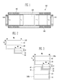
- FIG. 1 is a schematic plan view describing a driving circuit for a flat panel display device according to some exemplary embodiments.
- FIG. 2 is a plan view describing a channel amplifier according to some embodiments. the exemplary embodiment.
- FIG. 3 is a plan view describing a arrangement structure of the channel amplifier according to some embodiments.
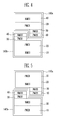
- FIGS. 4 and 5 are plan views showing examples of arrangements of the channel amplifiers and arrangements of the respective regions according to some embodiments.
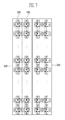
- FIG. 6 is a plan view showing the arrangement structure of FIG. 4 or 5 in more detail.
- FIG. 7 is a plan view describing a comparative example.
- first element When a first element is described as being coupled to a second element, the first element may be directly coupled to the second element or may be indirectly coupled to the second element via a third element. Further, some of the elements that are not essential to the complete understanding of the invention are omitted for clarity. Also, like reference numerals generally refer to like elements throughout.
- FIG. 1 is a schematic plan view describing a driving circuit of a flat panel display device according to an exemplary embodiment.
- the driving circuit 100 includes a circuit unit 120 supplying power and processing a signal and a channel amplifier 140 amplifying the processed signal and outputting the amplified signal through a pad unit 160.
- a channel amplifier 140 amplifying the processed signal and outputting the amplified signal through a pad unit 160.
- Several hundred to several thousand of channel amplifiers 140 may be provided according to the resolution of the flat panel display device and may be disposed in the vicinity of the circuit unit 120.
- the driving circuit 100 may be configured to receive grayscale voltages corresponding to 64 grayscale, 128 grayscale, 256 grayscale, and the like, from a grayscale voltage generator (not shown) and select a grayscale voltage according to image data input from the outside to supply the grayscale voltage to a corresponding data line.
- a grayscale voltage generator not shown
- the circuit unit 120 supplies power for operating the driving circuit 100 and processes the image data input from the outside to generate the data signal, and the channel amplifier 140 amplifies the data signal and transfers the amplified signal to a corresponding data line.
- FIG. 2 is a plan view illustrating a channel amplifier 140 according to an exemplary embodiment.
- the channel amplifier 140 includes a first region 10 having a first width W1 and a first length L1, a second region 20 disposed on one side of the first region 10 and having the first width W1 and the first length L1, a third region 30 on one side of the second region 20 and having a second width W2 and a second length L2 different from the first width W1 and the first length L1, respectively, and a fourth region 40 on one side of the third region 30 and having the second width W2 and the second length L2.
- first width W1 and first length L1 are larger than the second width W2 and the second length L2, respectively, and the first width W1 is equal to or greater than the sum of the first length L1 and the second length L2.
- TFTs Different types of transistors
- N-type transistors or P-type transistors are divided into a group and disposed as the different types of transistors (TFTs) at the first to fourth regions 10 to 40, thereby making it possible to facilitate a layout (design) and effectively reduce the area.
- N-type transistors may be disposed in the first and third regions 10 and 30 and P-type transistors may be disposed in the second and fourth regions 20 and 40, or the N-type transistors may be disposed in the first and fourth regions 10 and 40 and the P-type transistors may be disposed in the second and third regions 20 and 30.
- the P-type transistors may be disposed in the first and third regions 10 and 30 and the N-type transistors may be disposed at the second and fourth regions 20 and 40, or the P-type transistors may be disposed in the first and fourth regions 10 and 40 and the N-type transistors may be disposed in the second and third regions 20 and 30.
- each region has only one type of transistor.
- a plurality of transistors at least partly forming circuits for amplifying the data signals and transferring the amplified signals to the plurality of data lines are each either N-type or P-type and are located in the first and second regions 10 and 20, and a plurality of transistors at least partly forming an input circuit and an output circuit are each either N-type or P-type and are located in the third and fourth regions 30 and 40.
- the channel amplifiers 140 may be arranged at upper and lower portions, as shown in FIG. 3 .
- the first and second regions 10 and 20 at the upper portion of the channel amplifier 140a and the first and second regions 10 and 20 at the lower portion of the channel amplifier 140b are vertically symmetrical to each other, and the third and fourth regions 30 and 40 of the channel amplifier 140a at the upper portion and the third and fourth regions 30 and 40 of the channel amplifier 140b at the lower portion are horizontally symmetrical to each other.
- FIGS. 4 and 5 are plan views showing examples of arrangements of the channel amplifiers 140a and 140b according to an exemplary embodiment.
- N-type transistors are in the first and third regions 10 and 30 of the channel amplifier 140a at the upper portion and P-type transistors (PMOS) are in the second and fourth regions 20 and 40 thereof, and the N-type transistors (NMOS) are in the first and fourth regions 10 and 40 of the channel amplifier 140b at the lower portion and the P-type transistors (PMOS) are in the second and third regions 20 and 30 thereof.
- the P-type transistors are in the first and fourth regions 10 and 40 of the channel amplifier 140a at the upper portion and the N-type transistors (NMOS) are in the second and third regions 20 and 30 thereof, and the P-type transistors (PMOS) are in the first and third regions 10 and 30 of the channel amplifier 140b at the lower portion and the N-type transistors (NMOS) are in the second and fourth regions 20 and 40 thereof.
- FIG. 6 which is a plan view showing the arrangement structure of FIG. 4 or FIG. 5 in more detail, shows an example of a structure in which gate (G) electrodes, source (S) electrodes, drain (D) electrodes, and wirings of the transistors (NMOS and PMOS) are in the first to fourth regions 10 to 40.
- the driving circuit in the flat panel display device has a rectangular shape in which one side (width) is larger than another side (length).
- one side (width) is larger than another side (length).
- a larger number of channel amplifiers are required, such that a size of the driving circuit is inevitably increased.
- the size is increased only at one side, several problems are generated.
- connection path between an N-type transistor of the first region 210 and a P-type transistor of the second region 220 is sufficiently short; however, a connection path between the transistors within each region 210 or 220 is undesirably long, and a channel width or length of each transistor is limited. As the number of channel amplifiers increases, these problems become more significant.
- the channel amplifier (See FIG. 6 ) according to the exemplary embodiments has a width greater than that of the channel amplifier of FIG. 7 and a length shorter than that of the channel amplifier of FIG. 7 , both the connection path between the transistor of the first region 10 and the transistor of the second region 20 and the connection path between the transistors within each region 10 or 20 may become short.
- the width of the respective regions 10 and 20 is wide, the channel width or length of each transistor may be effectively chosen and the area efficiently used.
- the channel amplifier of the FIG. 6 may have use less area as compared to the channel amplifier of FIG. 7 by about 20%.
- the channel amplifier (See FIG. 6 ) according to the exemplary embodiment is used, since the third and four regions 30 and 40 are adjacent to each other between the respective channel amplifiers 140a and 140b, when an input circuit and an output circuit are disposed at the third and four regions 30 and 40, an offset of the transistor is minimized and distances from the respective channel amplifiers to the pad unit 160 are substantially the same as each other, such that all of the channel amplifiers may maintain uniform input/output characteristics.
- both of the connection path between the transistor of one region and the transistor of another region and the connection path between the transistors within of the respective regions may be short.
- the widths of the respective regions are sufficient, the channel width or length of the channel of the each transistor may be sufficient and the space may also be efficiently used.
- the input circuit and output circuit are between each channel amplifier, an offset of the transistor is minimized, and the distances from the each channel amplifier to the pad unit are substantially the same as each other, such that all channel amplifiers may maintain uniform input/output characteristics.
Landscapes
- Engineering & Computer Science (AREA)
- Physics & Mathematics (AREA)
- Computer Hardware Design (AREA)
- General Physics & Mathematics (AREA)
- Theoretical Computer Science (AREA)
- Liquid Crystal Display Device Control (AREA)
- Control Of Indicators Other Than Cathode Ray Tubes (AREA)
- Design And Manufacture Of Integrated Circuits (AREA)
- Semiconductor Integrated Circuits (AREA)
- Metal-Oxide And Bipolar Metal-Oxide Semiconductor Integrated Circuits (AREA)
Abstract
Description
- This application claims priority to and the benefit of Korean Patent Application No.
10-2012-0107162, filed on September 26, 2012 - The disclosed technology relates to a flat panel display device, and more particularly, to a layout of a driving circuit used in a flat panel display device.
- Generally, a flat panel display device such as a liquid crystal display (LCD), an organic light emitting diode (OLED), and the like, includes a display panel in which a plurality of pixels are arranged, and a driving circuit for displaying an image on the display panel by driving the plurality of pixels. Since the driving circuit generally includes an integrated circuit, it is called a display driver IC (DDI).
- The display panel includes pixels connected to each other in, for example, a matrix. Each pixel is at least partially between two scan lines and two date lines, and the driving circuit (DDI) includes a scan driving circuit for driving the scan lines and a data driving circuit for driving the data lines. Scan signals are sequentially supplied from the scan driving circuit to the plurality of scanning lines, such that the pixel is selected, and data signals are supplied from the data driving circuit to the data line connected with the selected pixel, such that an image is displayed.
- The driving circuit is configured to receive grayscales voltages, corresponding to 64 grayscale, 128 grayscale, 256 grayscale, and the like, from a grayscales voltage generator and select one of the grayscale voltages according to image data input from the outside to supply the selected grayscale voltage to a corresponding data line.
- In order to perform an operation as described above, the driving circuit includes a digital to analog converter converting digital image data into an analog signal and a channel amplifier for transmitting the selected grayscale voltage to the data line.
- Generally, several hundred to several thousand channel amplifiers are required. In addition, since the digital to analog converter and the channel amplifier include a large number of thin film transistors (TFTs) and complicated wiring, they occupy a large layout area.
- Recently, in accordance with a continuous increase in resolution of the flat panel display device, the number of scan lines and data lines has increased. Therefore, the area occupied by the driving circuit has rapidly increased. However, since the area occupied by the driving circuit in the flat panel display device is limited, it is difficult to efficiently layout (design) the driving circuit in the limited area.
- One inventive aspect is an amplifier circuit according to claim 1 for a driving circuit for a flat panel display device. The amplifier circuit includes a first region having a first width and a first length, a second region on one side of the first region and having the first width and the first length, and a third region on one side of the second region and having a second width and a second length, wherein the second width and the second length are different from the first width and the first length. The driving circuit also includes a fourth region on one side of the third region and having the second width and the second length, wherein each region has one or more transistors of only one type. Advantageous embodiments of the amplifier circuit are specified in the claims dependent on claim 1.
- Another inventive aspect is a driving circuit according to
claim 10 for a flat panel display device. The driving circuit includes first and second amplifier circuits according to the invention. Advantageous embodiments of the driving circuit are specified in the claims dependent onclaim 10. - The accompanying drawings, together with the specification, illustrate exemplary embodiments, and, together with the description, serve to explain certain aspects and principles of the present invention.
-
FIG. 1 is a schematic plan view describing a driving circuit for a flat panel display device according to some exemplary embodiments. -
FIG. 2 is a plan view describing a channel amplifier according to some embodiments. the exemplary embodiment. -
FIG. 3 is a plan view describing a arrangement structure of the channel amplifier according to some embodiments. -
FIGS. 4 and 5 are plan views showing examples of arrangements of the channel amplifiers and arrangements of the respective regions according to some embodiments. -
FIG. 6 is a plan view showing the arrangement structure ofFIG. 4 or 5 in more detail. -
FIG. 7 is a plan view describing a comparative example. - Hereinafter, certain exemplary embodiments are described with reference to the accompanying drawings. When a first element is described as being coupled to a second element, the first element may be directly coupled to the second element or may be indirectly coupled to the second element via a third element. Further, some of the elements that are not essential to the complete understanding of the invention are omitted for clarity. Also, like reference numerals generally refer to like elements throughout.
- Hereinafter, certain embodiments are described with reference to the accompanying drawings. The following exemplary embodiments may be modified in many different forms so that those skilled in the art may implement the various features and aspects, and the scope of the present invention should not be limited to the embodiments to be described below.
-
FIG. 1 is a schematic plan view describing a driving circuit of a flat panel display device according to an exemplary embodiment. Referring toFIG. 1 , thedriving circuit 100 includes acircuit unit 120 supplying power and processing a signal and achannel amplifier 140 amplifying the processed signal and outputting the amplified signal through apad unit 160. Several hundred to several thousand ofchannel amplifiers 140 may be provided according to the resolution of the flat panel display device and may be disposed in the vicinity of thecircuit unit 120. - In the case in which the
driving circuit 100 is operated as a data driving circuit, it may be configured to receive grayscale voltages corresponding to 64 grayscale, 128 grayscale, 256 grayscale, and the like, from a grayscale voltage generator (not shown) and select a grayscale voltage according to image data input from the outside to supply the grayscale voltage to a corresponding data line. - The
circuit unit 120 supplies power for operating thedriving circuit 100 and processes the image data input from the outside to generate the data signal, and thechannel amplifier 140 amplifies the data signal and transfers the amplified signal to a corresponding data line. -
FIG. 2 is a plan view illustrating achannel amplifier 140 according to an exemplary embodiment. Referring toFIG. 2 , thechannel amplifier 140 includes afirst region 10 having a first width W1 and a first length L1, asecond region 20 disposed on one side of thefirst region 10 and having the first width W1 and the first length L1, athird region 30 on one side of thesecond region 20 and having a second width W2 and a second length L2 different from the first width W1 and the first length L1, respectively, and afourth region 40 on one side of thethird region 30 and having the second width W2 and the second length L2. - In this embodiment, the first width W1 and first length L1 are larger than the second width W2 and the second length L2, respectively, and the first width W1 is equal to or greater than the sum of the first length L1 and the second length L2.
- Different types of transistors (TFTs) are disposed in the
first region 10, thesecond region 20, thethird region 30, andfourth region 40, respectively. N-type transistors or P-type transistors are divided into a group and disposed as the different types of transistors (TFTs) at the first tofourth regions 10 to 40, thereby making it possible to facilitate a layout (design) and effectively reduce the area. - For example, N-type transistors may be disposed in the first and
third regions fourth regions fourth regions third regions - Alternatively, the P-type transistors may be disposed in the first and
third regions fourth regions fourth regions third regions - Accordingly, in these embodiments, each region has only one type of transistor.
- A plurality of transistors at least partly forming circuits for amplifying the data signals and transferring the amplified signals to the plurality of data lines are each either N-type or P-type and are located in the first and
second regions fourth regions - It may be advantageous that the
channel amplifiers 140 may be arranged at upper and lower portions, as shown inFIG. 3 . In this configuration, the first andsecond regions channel amplifier 140a and the first andsecond regions channel amplifier 140b are vertically symmetrical to each other, and the third andfourth regions channel amplifier 140a at the upper portion and the third andfourth regions channel amplifier 140b at the lower portion are horizontally symmetrical to each other. -
FIGS. 4 and 5 are plan views showing examples of arrangements of thechannel amplifiers - Referring to
FIG. 4 , N-type transistors (NMOS) are in the first andthird regions channel amplifier 140a at the upper portion and P-type transistors (PMOS) are in the second andfourth regions fourth regions channel amplifier 140b at the lower portion and the P-type transistors (PMOS) are in the second andthird regions - Referring to
FIG. 5 , the P-type transistors (PMOS) are in the first andfourth regions channel amplifier 140a at the upper portion and the N-type transistors (NMOS) are in the second andthird regions third regions channel amplifier 140b at the lower portion and the N-type transistors (NMOS) are in the second andfourth regions -
FIG. 6 , which is a plan view showing the arrangement structure ofFIG. 4 or FIG. 5 in more detail, shows an example of a structure in which gate (G) electrodes, source (S) electrodes, drain (D) electrodes, and wirings of the transistors (NMOS and PMOS) are in the first tofourth regions 10 to 40. - It may be advantageous that the driving circuit in the flat panel display device has a rectangular shape in which one side (width) is larger than another side (length). In accordance with an increase in a resolution of the flat panel display device, a larger number of channel amplifiers are required, such that a size of the driving circuit is inevitably increased. However, when the size is increased only at one side, several problems are generated.
- For example, as shown in
FIG. 7 , when thefirst region 210 and thesecond region 220 are in parallel with each other in the length direction, there is a limitation in increasing the length. In addition, a connection path between an N-type transistor of thefirst region 210 and a P-type transistor of thesecond region 220 is sufficiently short; however, a connection path between the transistors within eachregion - On the other hand, since the channel amplifier (See
FIG. 6 ) according to the exemplary embodiments has a width greater than that of the channel amplifier ofFIG. 7 and a length shorter than that of the channel amplifier ofFIG. 7 , both the connection path between the transistor of thefirst region 10 and the transistor of thesecond region 20 and the connection path between the transistors within eachregion respective regions FIG. 6 may have use less area as compared to the channel amplifier ofFIG. 7 by about 20%. - In addition, in the case in which the channel amplifier (See
FIG. 6 ) according to the exemplary embodiment is used, since the third and fourregions respective channel amplifiers regions pad unit 160 are substantially the same as each other, such that all of the channel amplifiers may maintain uniform input/output characteristics. - Since the width and the length of the channel amplifier according to the exemplary embodiment are substantially the same as each other, both of the connection path between the transistor of one region and the transistor of another region and the connection path between the transistors within of the respective regions may be short. In addition, since the widths of the respective regions are sufficient, the channel width or length of the channel of the each transistor may be sufficient and the space may also be efficiently used. Further, since the input circuit and output circuit are between each channel amplifier, an offset of the transistor is minimized, and the distances from the each channel amplifier to the pad unit are substantially the same as each other, such that all channel amplifiers may maintain uniform input/output characteristics.
- While various aspects and features have been described in connection with certain exemplary embodiments, it is to be understood that the invention is not limited to the disclosed embodiments, but, on the contrary, is intended to cover various modifications and equivalent arrangements.
Claims (15)
- An amplifier circuit (140, 140a, 140b) for a driving circuit (100) for a flat panel display device, the driving circuit comprising:a first region (10) having a first width (W1) and a first length (L1);a second region (20) on one side of the first region and having the first width (W1) and the first length (L1);a third region (30) on one side of the second region and having a second width and (W2) a second length (L2), wherein the second width (W2) and the second length (L2) are different from the first width (W1) and the first length (L1); anda fourth region (40) on one side of the third region and having the second width (W2) and the second length (L2),wherein each region (10, 20, 30, 40) has one or more transistors of only one type.
- The amplifier circuit (140, 140a, 140b) according to claim 1, wherein the first width (W1) and the first length (L1) are greater than the second width (W2) and the second length (L2), respectively.
- The amplifier circuit (140, 140a, 140b) according to claim 1 or 2, wherein the first width (W1) is equal to or greater than the sum of the first length (L1) and the second length (L2).
- The amplifier circuit (140, 140a, 140b) according to one of the preceding claims, wherein the first and third regions (10, 30) comprise transistors of a first type andthe second and fourth regions (20, 40) comprise transistors of a second type different from the first type.
- The amplifier circuit (140, 140a, 140b) according to one of claims 1- 3, wherein first and fourth regions (10, 40) comprise transistors of a first type andthe second and third regions (20, 30) comprise transistors of a second type different from the first type.
- The amplifier circuit (140, 140a, 140b) according to claim 4 or 5, wherein the transistors of the first type are P-type transistors.
- The amplifier circuit (140, 140a, 140b) according to claim 4 or 5, wherein the transistors of the second type are P-type transistors.
- The amplifier circuit (140, 140a, 140b) according to one of the preceding claims, wherein an input circuit is at least partly formed by the transistors of the third region (30) and an output circuit is at least partly formed by the transistors of the fourth region (40).
- The amplifier circuit (140, 140a, 140b) according to one of claims 1 to 7, wherein an output circuit is at least partly formed by the transistors of the third region (30) and an input circuit is at least partly formed by the transistors of the fourth region (40).
- The amplifier circuit (140, 140a, 140b) according to one of the preceding claims, wherein each of the first, second, third, and fourth region has a rectangular shape.
- A driving circuit (100) comprising a first amplifier circuit (140a) according to one of the preceding claims and a second amplifier circuit (140b) according to one of the preceding claims.
- The driving circuit (100) according to claim 11, wherein the first regions of the first amplifier circuit (140a) and of the second amplifier circuit (140b) comprise transistors of a same type.
- The driving circuit (100) according to claim 11 or 12, wherein the third region (30) of the first amplifier (140a) is adjacent to the fourth region (40) of the second amplifier (140b), and wherein the fourth region (40) of the first amplifier (140a) is adjacent to the third region (30) of the second amplifier (140b).
- The driving circuit (100) according to claim 13 wherein the first and second regions (10, 20) of the first amplifier circuit (140a) and the first and second regions (10, 20) of the second amplifier circuit (140b) are vertically symmetrical to each other, and the third and fourth regions (30, 40) of the first amplifier circuit (140a) and the third and fourth regions (30, 40) of the second amplifier circuit (140b) are horizontally symmetrical to each other.
- The driving circuit (100) according to one of claims 11 to 14 wherein the driving circuit (100) has a rectangular shape in which a width of the driving circuit (100) is larger than a length of the driving circuit (100).
Applications Claiming Priority (1)
| Application Number | Priority Date | Filing Date | Title |
|---|---|---|---|
| KR1020120107162A KR102008878B1 (en) | 2012-09-26 | 2012-09-26 | Driving circuit for flat panel display device |
Publications (1)
| Publication Number | Publication Date |
|---|---|
| EP2713358A1 true EP2713358A1 (en) | 2014-04-02 |
Family
ID=48013854
Family Applications (1)
| Application Number | Title | Priority Date | Filing Date |
|---|---|---|---|
| EP13161938.9A Ceased EP2713358A1 (en) | 2012-09-26 | 2013-04-02 | Driving circuit for flat panel display device |
Country Status (6)
| Country | Link |
|---|---|
| US (1) | US20140085171A1 (en) |
| EP (1) | EP2713358A1 (en) |
| JP (1) | JP6181387B2 (en) |
| KR (1) | KR102008878B1 (en) |
| CN (1) | CN103680380B (en) |
| TW (1) | TWI589956B (en) |
Families Citing this family (2)
| Publication number | Priority date | Publication date | Assignee | Title |
|---|---|---|---|---|
| US12142211B2 (en) | 2021-09-15 | 2024-11-12 | Yunnan Invensight Optoelectronics Technology Co., Ltd. | Display substrate, pixel circuit, driving method and display apparatus |
| KR102815985B1 (en) * | 2022-11-07 | 2025-06-04 | 한양대학교 산학협력단 | Shared pixel circuit |
Citations (3)
| Publication number | Priority date | Publication date | Assignee | Title |
|---|---|---|---|---|
| US20050051853A1 (en) * | 2003-09-05 | 2005-03-10 | Baum David R. | Interdigitated layout methodology for amplifier and H-bridge output stages |
| JP2009170483A (en) * | 2008-01-11 | 2009-07-30 | Seiko Epson Corp | Sample hold circuit, integrated circuit device, electro-optical device, and electronic apparatus |
| US20110049575A1 (en) * | 2009-08-28 | 2011-03-03 | Sony Corporation | Semiconductor integrated circuit |
Family Cites Families (9)
| Publication number | Priority date | Publication date | Assignee | Title |
|---|---|---|---|---|
| JP2522806B2 (en) * | 1987-11-20 | 1996-08-07 | 富士通株式会社 | Method for manufacturing semiconductor device |
| JP3846057B2 (en) * | 1998-09-03 | 2006-11-15 | セイコーエプソン株式会社 | Electro-optical device drive circuit, electro-optical device, and electronic apparatus |
| JP3635972B2 (en) * | 1999-02-23 | 2005-04-06 | セイコーエプソン株式会社 | Electro-optical device drive circuit, electro-optical device, and electronic apparatus |
| JP4928675B2 (en) * | 2001-03-01 | 2012-05-09 | エルピーダメモリ株式会社 | Semiconductor device |
| JP4847702B2 (en) * | 2004-03-16 | 2011-12-28 | ルネサスエレクトロニクス株式会社 | Display device drive circuit |
| KR101010509B1 (en) * | 2004-05-31 | 2011-01-21 | 엘지디스플레이 주식회사 | LCD panel with integrated driving circuit |
| KR20100138146A (en) * | 2009-06-24 | 2010-12-31 | 삼성전자주식회사 | High Efficiency Charge Pump |
| KR20110085058A (en) * | 2010-01-19 | 2011-07-27 | 삼성전자주식회사 | Data line driver and devices containing it |
| JP5616762B2 (en) * | 2010-11-24 | 2014-10-29 | ルネサスエレクトロニクス株式会社 | Output circuit, data driver, and display device |
-
2012
- 2012-09-26 KR KR1020120107162A patent/KR102008878B1/en active Active
-
2013
- 2013-01-29 US US13/753,334 patent/US20140085171A1/en not_active Abandoned
- 2013-03-01 TW TW102107305A patent/TWI589956B/en active
- 2013-03-08 JP JP2013046549A patent/JP6181387B2/en active Active
- 2013-04-02 EP EP13161938.9A patent/EP2713358A1/en not_active Ceased
- 2013-09-10 CN CN201310409616.XA patent/CN103680380B/en active Active
Patent Citations (3)
| Publication number | Priority date | Publication date | Assignee | Title |
|---|---|---|---|---|
| US20050051853A1 (en) * | 2003-09-05 | 2005-03-10 | Baum David R. | Interdigitated layout methodology for amplifier and H-bridge output stages |
| JP2009170483A (en) * | 2008-01-11 | 2009-07-30 | Seiko Epson Corp | Sample hold circuit, integrated circuit device, electro-optical device, and electronic apparatus |
| US20110049575A1 (en) * | 2009-08-28 | 2011-03-03 | Sony Corporation | Semiconductor integrated circuit |
Non-Patent Citations (1)
| Title |
|---|
| CHARBON E ET AL: "IMPOSING TIGHT SPECIFICATIONS ON ANALOG IC'S THROUGH SIMULTANEOUS PLACEMENT AND MODULE OPTIMIZATION", PROCEEDINGS OF THE CUSTOM INTEGRATED CIRCUITS CONFERENCE. SAN DIEGO, MAY 1 - 4, 1994; [PROCEEDINGS OF THE CUSTOM INTEGRATED CIRCUITS CONFERENCE], NEW YORK, IEEE, US, vol. CONF. 16, 1 May 1994 (1994-05-01), pages 525 - 528, XP000492944 * |
Also Published As
| Publication number | Publication date |
|---|---|
| KR20140040466A (en) | 2014-04-03 |
| TW201413334A (en) | 2014-04-01 |
| JP2014067990A (en) | 2014-04-17 |
| JP6181387B2 (en) | 2017-08-16 |
| CN103680380A (en) | 2014-03-26 |
| CN103680380B (en) | 2018-01-19 |
| TWI589956B (en) | 2017-07-01 |
| US20140085171A1 (en) | 2014-03-27 |
| KR102008878B1 (en) | 2019-08-09 |
Similar Documents
| Publication | Publication Date | Title |
|---|---|---|
| CN115472127B (en) | Display Devices | |
| CN111048024B (en) | Display devices and display panels | |
| US10290275B2 (en) | Driving circuit for multiple GOA units minimizing display border width | |
| TWI514344B (en) | Display apparatus | |
| US10388208B2 (en) | Display device | |
| JP6370357B2 (en) | Display device | |
| EP3561801B1 (en) | Display panel | |
| US20100245300A1 (en) | Shift Register | |
| KR102262863B1 (en) | Gate driver ic, gate driving method, display panel, and display device | |
| CN111868807A (en) | display device | |
| US11676553B2 (en) | Reduced heat generation from a source driver of display device | |
| KR102687420B1 (en) | Display panel and display device | |
| KR20180079560A (en) | Display device, display panel, driving method, and gate driving circuit | |
| CN112634804B (en) | Gate driver and display device | |
| US20110175863A1 (en) | Data line driver and apparatuses having the same | |
| US10984709B2 (en) | Display panel | |
| EP2713358A1 (en) | Driving circuit for flat panel display device | |
| KR102140643B1 (en) | Display device | |
| CN111243500B (en) | Display panel | |
| JP2016009112A (en) | Display device | |
| KR102558898B1 (en) | Gip driving device and organic light emitting display comprising the same | |
| CN118571881A (en) | Display device and display panel | |
| KR20160126765A (en) | Driver ic | |
| JP2005183408A (en) | ELECTRO-OPTICAL DEVICE, DRIVE CIRCUIT THEREOF, AND ELECTRONIC DEVICE | |
| EP4589632A1 (en) | Display panel and display device |
Legal Events
| Date | Code | Title | Description |
|---|---|---|---|
| PUAI | Public reference made under article 153(3) epc to a published international application that has entered the european phase |
Free format text: ORIGINAL CODE: 0009012 |
|
| 17P | Request for examination filed |
Effective date: 20130402 |
|
| AK | Designated contracting states |
Kind code of ref document: A1 Designated state(s): AL AT BE BG CH CY CZ DE DK EE ES FI FR GB GR HR HU IE IS IT LI LT LU LV MC MK MT NL NO PL PT RO RS SE SI SK SM TR |
|
| AX | Request for extension of the european patent |
Extension state: BA ME |
|
| RAP1 | Party data changed (applicant data changed or rights of an application transferred) |
Owner name: SAMSUNG DISPLAY CO., LTD. |
|
| 17Q | First examination report despatched |
Effective date: 20151109 |
|
| STAA | Information on the status of an ep patent application or granted ep patent |
Free format text: STATUS: THE APPLICATION HAS BEEN REFUSED |
|
| 18R | Application refused |
Effective date: 20170919 |