EP2709162A1 - Photovoltaic cell and photovoltaic cell module based thereon - Google Patents
Photovoltaic cell and photovoltaic cell module based thereon Download PDFInfo
- Publication number
- EP2709162A1 EP2709162A1 EP12184211.6A EP12184211A EP2709162A1 EP 2709162 A1 EP2709162 A1 EP 2709162A1 EP 12184211 A EP12184211 A EP 12184211A EP 2709162 A1 EP2709162 A1 EP 2709162A1
- Authority
- EP
- European Patent Office
- Prior art keywords
- emitter
- base
- connector lines
- contact islands
- islands
- Prior art date
- Legal status (The legal status is an assumption and is not a legal conclusion. Google has not performed a legal analysis and makes no representation as to the accuracy of the status listed.)
- Withdrawn
Links
Images



Classifications
-
- H—ELECTRICITY
- H10—SEMICONDUCTOR DEVICES; ELECTRIC SOLID-STATE DEVICES NOT OTHERWISE PROVIDED FOR
- H10F—INORGANIC SEMICONDUCTOR DEVICES SENSITIVE TO INFRARED RADIATION, LIGHT, ELECTROMAGNETIC RADIATION OF SHORTER WAVELENGTH OR CORPUSCULAR RADIATION
- H10F77/00—Constructional details of devices covered by this subclass
- H10F77/20—Electrodes
- H10F77/206—Electrodes for devices having potential barriers
- H10F77/211—Electrodes for devices having potential barriers for photovoltaic cells
- H10F77/219—Arrangements for electrodes of back-contact photovoltaic cells
-
- H—ELECTRICITY
- H10—SEMICONDUCTOR DEVICES; ELECTRIC SOLID-STATE DEVICES NOT OTHERWISE PROVIDED FOR
- H10F—INORGANIC SEMICONDUCTOR DEVICES SENSITIVE TO INFRARED RADIATION, LIGHT, ELECTROMAGNETIC RADIATION OF SHORTER WAVELENGTH OR CORPUSCULAR RADIATION
- H10F10/00—Individual photovoltaic cells, e.g. solar cells
- H10F10/10—Individual photovoltaic cells, e.g. solar cells having potential barriers
- H10F10/14—Photovoltaic cells having only PN homojunction potential barriers
- H10F10/146—Back-junction photovoltaic cells, e.g. having interdigitated base-emitter regions on the back side
-
- H—ELECTRICITY
- H10—SEMICONDUCTOR DEVICES; ELECTRIC SOLID-STATE DEVICES NOT OTHERWISE PROVIDED FOR
- H10F—INORGANIC SEMICONDUCTOR DEVICES SENSITIVE TO INFRARED RADIATION, LIGHT, ELECTROMAGNETIC RADIATION OF SHORTER WAVELENGTH OR CORPUSCULAR RADIATION
- H10F71/00—Manufacture or treatment of devices covered by this subclass
- H10F71/121—The active layers comprising only Group IV materials
-
- H—ELECTRICITY
- H10—SEMICONDUCTOR DEVICES; ELECTRIC SOLID-STATE DEVICES NOT OTHERWISE PROVIDED FOR
- H10F—INORGANIC SEMICONDUCTOR DEVICES SENSITIVE TO INFRARED RADIATION, LIGHT, ELECTROMAGNETIC RADIATION OF SHORTER WAVELENGTH OR CORPUSCULAR RADIATION
- H10F77/00—Constructional details of devices covered by this subclass
- H10F77/10—Semiconductor bodies
- H10F77/14—Shape of semiconductor bodies; Shapes, relative sizes or dispositions of semiconductor regions within semiconductor bodies
- H10F77/148—Shapes of potential barriers
-
- Y—GENERAL TAGGING OF NEW TECHNOLOGICAL DEVELOPMENTS; GENERAL TAGGING OF CROSS-SECTIONAL TECHNOLOGIES SPANNING OVER SEVERAL SECTIONS OF THE IPC; TECHNICAL SUBJECTS COVERED BY FORMER USPC CROSS-REFERENCE ART COLLECTIONS [XRACs] AND DIGESTS
- Y02—TECHNOLOGIES OR APPLICATIONS FOR MITIGATION OR ADAPTATION AGAINST CLIMATE CHANGE
- Y02E—REDUCTION OF GREENHOUSE GAS [GHG] EMISSIONS, RELATED TO ENERGY GENERATION, TRANSMISSION OR DISTRIBUTION
- Y02E10/00—Energy generation through renewable energy sources
- Y02E10/50—Photovoltaic [PV] energy
- Y02E10/547—Monocrystalline silicon PV cells
-
- Y—GENERAL TAGGING OF NEW TECHNOLOGICAL DEVELOPMENTS; GENERAL TAGGING OF CROSS-SECTIONAL TECHNOLOGIES SPANNING OVER SEVERAL SECTIONS OF THE IPC; TECHNICAL SUBJECTS COVERED BY FORMER USPC CROSS-REFERENCE ART COLLECTIONS [XRACs] AND DIGESTS
- Y02—TECHNOLOGIES OR APPLICATIONS FOR MITIGATION OR ADAPTATION AGAINST CLIMATE CHANGE
- Y02P—CLIMATE CHANGE MITIGATION TECHNOLOGIES IN THE PRODUCTION OR PROCESSING OF GOODS
- Y02P70/00—Climate change mitigation technologies in the production process for final industrial or consumer products
- Y02P70/50—Manufacturing or production processes characterised by the final manufactured product
Definitions
- the present invention relates to a photovoltaic cell (solar cell) with at least one base of a first polarity and at least one emitter of a second polarity and having a front side for receiving light and a back side opposite said front side, wherein base contact structure elements contacting the at least one base and emitter contact structure elements contacting the at least one emitter are formed on said back side separately from each other; wherein the base contact structure elements are connected electrically by base connector lines provided on the base contact structure elements and the emitter contact structure elements are connected electrically by emitter connector lines provided on the emitter contact structure elements, wherein the base connector lines and the emitter connector lines extend longitudinally side by side, distanced from each other and alternately over the back side of the photovoltaic cell, respectively; the base contact structure elements and the emitter contact structure elements comprise base contact islands and emitter contact islands being spaced apart from each other; the base contact islands and the emitter contact islands have lengths extending longitudinally in a direction transverse to a longitudinal direction of the base connector lines and the emitter
- Photovoltaic cells consist typically of a semiconductor substrate, such as a silicon substrate, having a front side for receiving light and a back side opposite the front side.
- a semiconductor substrate such as a silicon substrate
- at least one semiconductor junction defined by junction-forming regions of first and second polarities is formed.
- the regions of first and second polarities are regions with n- or p-doping, respectively, and comprise at least one emitter with a first polarity and at least one base of a second polarity.
- IBC interdigitated back contact
- PV photovoltaic
- a first plurality of fingers 4 is formed on a PV substrate 1 of a conventional IBC solar cell 100 to connect n- or n + -doped regions of that substrate 1 and a second plurality of fingers 12 is formed on the PV substrate 1 to connect p- or p + -doped regions of that substrate 1.
- the first plurality of fingers 4 is connected by a bus bar 3 and the second plurality of fingers 12 is connected by a bus bar 2, the bus bars 2, 3 being provided on opposite margin sides of the substrate 1.
- the contact structures have a comb like shape.
- the fingers 4, 12 allow collecting and carrying the current generated in the PV cell on the overall back side surface of the solar cell to the bus bars.
- the bus bars 2, 3 act as external connection points for module interconnection of the solar cell 100.
- the fingers 4, 12 are long and narrow structures of a metal material such as silver and have a length approximately equal to one cell dimension. Typical fingers of the state of the art have a width of between about 50 to 150 ⁇ m, a height of about 2 to about 30 ⁇ m and a lateral spacing of between about 1 and 5 mm. Due to the small cross section of the fingers and their long length, the electrical performances of IBC solar cells are strongly sensitive to the current flow along these fingers.
- the described PV cell comprises first and second pluralities of exposed metal contact portions being arranged in a checkerboard pattern across the back side of the solar cell, said first and second pluralities of exposed metal contact portions connect corresponding semiconductor regions of the solar cell with first and second polarity, respectively.
- the first and the second plurality of exposed metal contact portions form a first and a second set with rows and columns, wherein these sets are spaced apart from each other in two orthogonal directions so that the exposed metal contact portions do not overlap.
- the exposed metal contact portions can be connected by parallel grid lines but can also be formed as physically separate elongate-shaped metal segments arranged in a plurality of parallel spaced apart lines extending across the back side of the solar cell.
- the metal segments have a length of about 1 to 3 mm, wherein the spacing between the rows is approximately equal to the length of the segments and the spacing to the next adjacent row of opposite polarity is about 0.5 to 3 mm.
- Each row of the first plurality of metal segments and each row of the second plurality of metal segments is connected, respectively, by an electrical conductor extending over the solar cell, wherein first and second sets of the electrical conductors connecting opposite doped semiconductor regions, respectively, are formed alternately and in parallel on the back side of the solar cell.
- the electrical conductors are strings having distal ends being connected with metallic foil bus bar formed on opposite sides to connect of the first set of electrical conductors and to connect the second set of electrical conductors. Thus, positive and negative terminals of the PV cell are formed.
- solar cells having an equal pattern of exposed metal portions but being associated with junction-forming regions of opposite polarity are placed adjacent to each other and connected by electrodes.
- the opposite arrangement of junction forming regions of the solar cells to connect can be provided by rotating the second solar cell 180 degrees relative to the orientation of the first solar cell. This way, the exposed metal contact portions on the first solar cell associated with the first polarity can be connected with the exposed metal contact portions of the second solar cell associated with the second polarity, and vice versa.
- the document US 2011/0041908 A1 discloses a rear contact solar cell, wherein elongate emitter regions and elongate base regions are provided in a semiconductor substrate in an interleaved manner on the surface of the rear side of the solar cell.
- the emitter and base regions are contacted by a coarse mesh of elongate emitter and base contacts that extend in a right angle thereto.
- the emitter and base contacts cover the emitter and base regions over relatively broad regions.
- the emitter contacts overlap base regions and the base contacts overlap emitter regions. Therefore, an electrically insulating layer is provided in the vertical direction between the emitter contacts and the base regions and between the base contacts and the emitter regions.
- the contacts contact locally the emitter and base regions, respectively, positioned under the insulating layer merely at openings in the insulating layer.
- This kind of solar cell provides good current collecting properties but needs a lot of steps for the contact formation leading to increased costs of manufacturing.
- the object is solved by a solar cell of the above mentioned type wherein the base connector lines and the emitter connector lines have such a width in the direction transverse to the longitudinal direction of the base and emitter connector lines that there is a direct contact between each of the connector lines and the corresponding base contact islands and emitter contact islands over the full width of the connector lines in the regions where the base connector lines cross the base contact islands and in the regions where the emitter connector lines cross the emitter connector islands, respectively, wherein the base connector lines do not overlap the emitter contact islands in the direction transverse to the longitudinal direction of the base and emitter connector lines and the emitter connector lines do not overlap the base contact islands in the direction transverse to the longitudinal direction of the base and emitter connector lines. That means, the connector lines are smaller in width than the distance between contact islands of same polarity.
- the present invention suggests the use of contact islands to contact the differently doped regions of the solar cell.
- the base and emitter contact structure elements of the present invention are interrupted into short sections named contact islands.
- the contact islands are arranged in such a way and have such a length that those contact islands which contact semiconductor regions with opposite polarity interfinger.
- the present invention leads to a decrease of ohmic losses per "finger" without using thick metallization for forming the base and emitter contact structure elements.
- the current flows only through half the island length before being collected by a connector line such as a perpendicular ribbon. Therefore, the ohmic losses of the contact islands can be strongly reduced.
- the length of the contact islands used in the present invention can be for instance about 1/8 the length of a conventional finger, and the height of these contact islands can be strongly reduced in comparison to standard IBC solar cells, too.
- the height of fingers used in standard IBC solar cells is about 30 ⁇ m
- the height of the contact islands used in the present invention can be of about 0.5 ⁇ m. This leads to a benefiting reduction of the serial resistance of the corresponding solar cell.
- the current from the underlying doped regions can be collected in a very efficient manner.
- the size of the solar cell can be optimized.
- the possibility to use extremely thin - that means only several 100 nanometers thick - metal layers for forming the contact islands leads to the opportunity to deposit these layers by means of technologies like screen printing, sputtering or evaporation without plating.
- the manufacturing costs can be reduced thanks to the material consumption saving.
- connector lines used in the present invention are so small in width that these lines do not overlap the contact islands in the direction transverse to the longitudinal direction of the base and emitter connector lines, an undesired short circuit between the different types of contacts can be prevented in an uncomplicated way.
- the photovoltaic cell of the present invention there is no electrical insulator layer between the base connector lines and the corresponding base contact islands and between the emitter connector lines and the corresponding emitter contact islands. That means, in the vertical direction of the photovoltaic cell it is not necessary to separate the base connector lines from the emitter connector lines by an insulator. This is possible because, in according with the present invention, the connector lines do not overlap the contact islands in the direction transverse to the longitudinal direction of the base and emitter connector lines. Thus, there is enough space between the different contacts and the corresponding connector lines to prevent short circuits without the necessity of an additional insulator layer. That facilitates the manufacturing of the photovoltaic cell of the present invention considerably, e.g.
- an electrical insulator is provided in the vertical direction between regions of the contact islands and the base and the emitter regions. Additionally or alternatively, insulating areas covering edge regions of adjacent emitter contact islands and being formed under and along base connector lines extending between said adjacent emitter contact islands and insulating areas covering edge regions of adjacent base contact islands and being formed under and along emitter connector lines extending between said adjacent base contact islands can be provided.
- the electrical insulator between the different contact islands helps to avoid a contact between the respective connector line (wire) and the inter-contact area.
- the insulating areas provided in the regions along the base and emitter connector lines, respectively, serve to avoid any short circuit between the contact islands of different polarity, e. g. due to a misalignment of the connector lines during contacting.
- the connector lines can be formed from an electrical conducting material being able to be soldered, glued, taped or pressed on the photovoltaic cell.
- the base connector lines and the emitter connector lines are ribbons extending perpendicular to the length-extension of the contact islands. These ribbons are electrically connected to contact islands of one polarity, respectively.
- the ribbons can be placed on the solar cell during the cells interconnection. Ribbons are available with a small width so that these ribbons are very well suited to fulfill the requirement to the connector lines of the present invention, namely to have a width being as small that overlapping of the emitter contact islands in the direction transverse to the longitudinal direction of the base and emitter connector lines can be excluded.
- the base connector lines and the emitter connector lines have width being in the region between 10 ⁇ m und 1 mm, favorably between 10 ⁇ m and 500 ⁇ m. More preferably, the width of the base connector lines and the emitter connector lines is between 50 ⁇ m and 300 ⁇ m. Exemplarily, the width of the base connector lines and the emitter connector lines is between 100 ⁇ m and 250 ⁇ m.
- the base contact islands and the emitter contact islands are arranged separate from each other, wherein groups of base contact islands are connected by the crossing base connector lines, respectively, and groups of emitter contact islands are connected by the crossing emitter connector lines, respectively.
- interconnections are connected electrically in the level of the contact islands by interconnections, respectively, wherein the interconnections extend in the longitudinal directions of the base connector lines and the emitter connector lines, respectively.
- the interconnections are formed by the same material with the same doping as the material and the doping of the contact islands to be connected with the interconnection.
- the interconnections are part of the active regions of the photovoltaic cell.
- the contact islands may have a thickness of between 10 nm and 10 ⁇ m. Furthermore, the contact islands may have a width in their extension parallel to the longitudinal direction of the connector lines of between 1 ⁇ m and 5 mm.
- the base contact structure elements and the emitter contact structure elements may have a distance from each other of between 1 ⁇ m and 5 mm. Moreover, the distance of contact islands of same polarity in a direction transverse to the longitudinal direction of the connector lines can be between 10 ⁇ m and 5 mm.
- the base contact structure elements and the emitter contact structure elements consist of at least one material of the group of materials comprising silver, aluminum, copper, nickel, and vanadium.
- the base connector lines and the emitter connector lines are formed on or in or are covered by a film reflecting light into the photovoltaic cell.
- a photovoltaic cell module comprising at least two photovoltaic cells being formed in accordance with the present invention and being electrically connected with each other, wherein a bus bar is provided between two adjacent photovoltaic cells and interconnects the connector lines, such as ribbons, of the adjacent photovoltaic cells in such a way that connector lines connecting substrate regions of different polarities are connected.
- a photovoltaic cell module comprising at least two photovoltaic cells being formed in accordance with the present invention and being electrically connected with each other, wherein adjacent photovoltaic cells have comparable island patterns, but inversed island polarity, and wherein the adjacent photovoltaic cells are connected in such a way that a base connector line of one photovoltaic cell is continued over an adjacent photovoltaic cell to form there an emitter connector line of said adjacent photovoltaic cell.
- connector lines such as ribbons, connecting one polarity of contact islands of a first solar cell are directly connected to opposite polarity of a following solar cell.
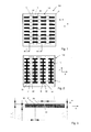
- Fig. 1 schematically shows a back side of a photovoltaic cell or solar cell 101 of the present invention.
- the solar cell 101 is in the embodiment shown formed from a crystalline silicon substrate 1 with a back side contact structure.
- the solar cell 101 can also be formed of another semiconductor material.
- the invention can be applied on all solar cell fabrication technologies using semiconductor with different doping type.
- the solar cell 101 can be a hetero junction solar cell.
- the back side contact structure of the solar cell 101 comprises interdigitated base contact structure elements 5 and emitter contact structure elements 6 being formed to connect underlying differently doped regions of the solar cell 101 forming the base and the emitter of that solar cell 101.
- the base contact structure elements 5 comprise base contact islands 50 and the emitter contact structure elements 6 comprise emitter contact islands 60 distributed in a staggered manner on the back side 14 of the solar cell 101.
- Adjacent contact islands 50, 50 or 60, 60 of same polarity as well as the contact islands 50, 60 of different polarity are spaced apart from each other. None of the contact islands 50, 60 overlap.
- the base contact islands 50 and the emitter contact islands 60 are arranged in rows and columns.
- the base contact islands 50 form a grid of base contact islands and the emitter contact islands 60 form a grid of emitter contact islands wherein the grids are staggered to each other.
- the base contact islands 50 and the emitter contact islands 60 have an elongated structure.
- the contact islands 50, 60 have a relatively high length to width ratio and a high length to thickness (height) ration.
- the lengths L 1 , L 2 of the base and the emitter contact islands 50, 60 are chosen in such a way that the base contact islands 50 and the emitter contact islands 60 interfinger.
- the contact islands 50, 60 can contact large areas of the doped regions of the solar cell 101 despite of a decreased place requirement of the respective contact islands 50, 60.
- Fig. 2 schematically shows a further embodiment of a solar cell 102 of the present invention with a view on the back side 14 of the solar cell 102.
- the solar cell 102 comprises interdigitated base contact structure elements 5' and emitter contact structure elements 6' contacting corresponding base and emitter regions formed in the solar cell 102 with different doping.
- the base contact structure elements 5' comprise base contact islands 50 being similar to the base contact islands 50 of the solar cell 101 of Fig. 1 . Therefore reference is made here to the above description of these base contact islands 50.
- the base contact islands of the embodiment of Fig. 2 are interconnected in the same level as the base contact islands 50 via interconnections 51.
- the emitter contact structure elements 6' comprise emitter contact islands 60 being similar to the emitter contact islands 60 of the solar cell 101 of Fig. 1 . Therefore reference is made here to the above description of these emitter contact islands 60.
- the emitter contact islands of the embodiment of Fig. 2 are interconnected in the same level as the emitter contact islands 60 via interconnections 61.
- the interconnected base and emitter contact islands 50, 60 form groups of base contact islands and groups of emitter contact islands wherein each group forms a pattern of several interconnected "H"'s.
- the "H” pattern ensures a better islands interconnection and a larger electrical connection between the contact islands 50, 60 and the corresponding connector lines 7, 8, as shown in Figs. 4 and 5 .
- the contact islands 50, 60 have a thickness (height) of between 10 nm and 10 ⁇ m. Furthermore, the contact islands 50, 60 have in the shown example a width in their extension in the direction B of between 1 ⁇ m and 5 mm. Typical amounts for this width are between 100 ⁇ m and 500 ⁇ m.
- the lengths L 1 , L 2 of the contact islands 50, 60 can be in a mm to cm range. A typical value for these lengths is about 2 cm.
- the base contact structure elements 5, 5' and the emitter contact structure elements 6, 6' have exemplarily a distance from each other of between 1 ⁇ m and 5 mm, preferably in the ⁇ m range, typically of about 100 ⁇ m. Moreover, the distance between contact islands 50, 60 of same polarity in the direction A parallel to the lengths L 1 , L 2 of the contact islands 50, 60 is between about 10 ⁇ m and about 5 mm, typically about 1 mm.
- Fig. 3 shows more specifically but only exemplarily possible dimensions by means of a detail of the solar cell 102 of Fig. 2 .
- the width of the interconnections 51, 61 is about 1 mm
- the width of the contact islands 50, 60 is about 0.4 mm
- the distance of the contact islands 50, 60 in the direction B transverse to the direction A of the lengths of the contact islands 50, 60 is about 0.2 mm.
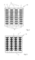
- Fig. 4 schematically shows the solar cell 101 of Fig. 1 with base connector lines 7 and emitter connector lines 8 connecting groups of base contact islands 50 and groups of emitter contact islands 60, respectively, in the vertical direction B of the shown solar cell 101.
- the respective connector lines 7, 8 connect only contact islands of one polarity. That means, the connector lines 7, 8 are provided in such a way that the base connector lines 7 do not cross the emitter contact islands 60 and that the emitter connector lines 8 do not cross the base contact islands 50.
- the base connector lines 7 and the emitter connector lines 8 are arranged in parallel and in an alternate manner so that columns of connected base contact islands 50 alternate with columns of connected emitter contact islands 60.
- Each of the base and emitter connector lines 7, 8 has two distal ends wherein one distal end ends on the substrate 1 and the other distal end protrudes from a side of the substrate 1, wherein the protruding ends of the base connector lines 7 protrude from one side of the substrate 1 and the protruding ends of the emitter connector lines 8 protrude from the opposite side of the substrate 1.
- ribbons are used as base and emitter connector lines 7, 8, preferably ribbons are used.
- the expression ribbon corresponds to any electrical material of any shape, such as rectangular or round, that can be soldered, glued, taped or just pressed on the solar cell.
- Fig. 5 schematically shows the solar cell 102 of Fig. 2 with base connector lines 7 and emitter connector lines 8 connecting the "H" patterned groups of base and emitter contact islands 50, 60, respectively.
- the base connector lines 7 extend on the interconnections 51 and the emitter connector lines 8 extend on the interconnections 61 so that the "H" patterned groups of base and emitter contact islands 50, 60 can be connected to corresponding groups of an adjacent solar cell (not shown).
- the base and emitter connector lines 7, 8 protrude for this from opposite sides of the substrate 1.
- Fig. 6 schematically shows an embodiment of a solar cell module 111 in accordance with the present invention.
- the solar cell module 111 consists of a plurality of adjacent solar cells 101 a, 101b, 101c being similar to the solar cell 101 of Fig. 1 .
- solar cells being similar to the solar cell 102 of Fig. 2 can also be used.
- the solar cells 101 a, 101 b, 101 c are placed side by side wherein bus bars 11a, 11b, 11c, 11d are provided at the margins and between adjacent solar cells 101, 101.
- Fig. 7 schematically shows another embodiment of a solar cell module 112 in accordance with the present invention wherein solar cells 101 a, 101'b with same or similar pattern but different distribution of polarities of the junction forming regions in the solar cells 101 a, 101'b are placed directly side by side and connected with each other by connector lines 7, 8.
- the connector lines 7, 8 form on one solar cell 101a base connector lines and form on the adjacent solar cell 101'b emitter connector lines and vice versa, since the connector lines 7, 8 extend on both adjacent solar cells 101a, 101'b, respectively.
- the solar cell module 112 is composed by alternating solar cells 101 a, 101'b, and only vertical connector lines 7, 8, such as ribbons, connect the solar cells 101 a, 101'b together. External bus bars are here not necessary.
- this technique of interconnection allows using a smaller space between the solar cells 101a, 101'b, improving the final power density of the solar cell module 112.
- the base connector lines 7 and the emitter connector lines 8 are formed on or in or are covered by a film reflecting light into the solar cell 101, 102.
- the film reflecting light is a so-called "white film”. That film can already receive the ribbons used as connector lines and then provided on the solar cell 101, 102 for concurrent interconnection and encapsulation.
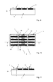
- Fig. 8 schematically shows a view of a back side of a solar cell of the present invention.
- the solar cell of Fig. 8 comprises emitter contact islands 60 being electrically connected with emitter regions formed in the substrate of the solar cell and base contact islands 50 being electrically connected with base regions being also formed in the substrate of the solar cell.
- Groups of emitter contact islands 60 and groups of base contact islands 50 are connected, respectively, by emitter connector lines 8 and base connector lines 7 leading as straight wires over the emitter contact islands 60 and the base contact islands 50 of the respective group of contact islands 50, 60.
- the electrical connection between the contact islands 50, 60 and the corresponding base and emitter regions in the substrate of the solar cell is not provided over the whole lengths of the contact islands 50, 60.
- an electrical insulator 9 is provided vertically as well as horizontally between the contact islands 50, 60.
- the electrical insulator 9 helps to avoid shunting due to a contact of the connector lines 7, 8 and the inter-contact area, that means between the wire(s) connecting the contact islands 50, 60 and amorphous or microcrystalline semiconductor areas of the solar cell, such as an intrinsic amorphous Si:H-layer formed in the substrate of the solar cell.
- Fig. 9 schematically shows a non-true-to-scale sectional side view of the solar cell of Fig. 8 taken along the direction A - A.
- the section shown goes through the length direction of the emitter contact islands 60.
- the emitter connector lines 8 lie directly on the emitter contact islands 60.
- the base connector lines 7 lie on the electrical insulator 9 formed between the emitter contact islands 60.
- the base connector lines 7 lie on the base contact islands 50, wherein the emitter connector lines 8 lie on the electrical insulator 9 formed between the base contact islands 50.
- the electrical insulator 9 does not only separate the contact islands 50, 50 and 60, 60 of one type and the contact islands different types 50, 60 from each other.
- the electrical insulator 9 further holds the base connector lines 7 and the emitter connector lines 8 on top of the electrical insulator 9. Since the electrical insulator 9 fills the gap between the contact islands 50, 50; 60, 60 and 50, 60, the base connector lines 7 and the emitter connector lines 8 do not lie in such a gap. Thus, a shunt contact between the emitter connector lines 8 and the base contact islands 50 as well as between the base connector lines 7 and the emitter contact islands 60 can be extensively prevented.
- Fig. 10 schematically shows a view on the back side of a further variant of the solar cell of the present invention.
- the solar cell of Fig. 10 comprises stripes of additional insulator areas 10, 10' being formed along the base and emitter connector lines 7, 8, respectively.
- the insulating areas 10 cover edge regions of adjacent emitter contact islands 60 of groups of emitter contact islands 60 lying vis-á-vis, respectively.
- the additional insulating areas 10 are formed under and along base connector lines 7 extending between said adjacent emitter contact islands 60.
- the insulating areas 10' cover edge regions of adjacent base contact islands 50 and are formed under and along emitter connector lines 8 extending between said adjacent base contact islands 50.
- the additional insulating areas 10, 10' which cover at least partially the contact islands 50, 60 of opposite polarity help to avoid a shunt between the base contact islands 50 and the emitter contact islands 60 due to an eventual misalignment of the connector lines 7, 8 during contacting.
- Fig. 11 schematically shows a non-true-to-scale sectional side view of the solar cell of Fig. 10 taken along the direction B - B.
- the section shown goes through the length direction of the emitter contact islands 60.
- the base connector lines 7, 7' lie - in comparison to the embodiment shown in Fig. 9 - now on top of the insulating areas 10. Therefore, there is an additional vertical distance between the base connector lines 7 and the emitter contact islands 60 and, accordingly, between the base connector lines 7 and the emitter connector lines 8.
- the emitter connector lines 8 lie on top of the additional insulating areas 10' and the base connector lines 7 rest on the base contact islands 50.
- this section exists also a larger vertical distance between the higher positioned emitter connector lines 8 and the lower positioned base contact islands 50 and base connector lines 7. That larger distance helps in particular in the case of a misalignment of connector lines such as the base connector line 7' in Fig. 11 .
- the base connector line 7' is not aligned in the middle of the horizontal distance between adjacent emitter contact islands 60. Nevertheless, there is an electrical separation between the base connector line 7' and emitter contact island 60 lying thereunder by the insulating area 10, because that insulating area 10 covers not only the electrical insulator 9 but also overlaps side parts of the adjacent emitter contact islands 60.
Landscapes
- Photovoltaic Devices (AREA)
Abstract
Description
- The present invention relates to a photovoltaic cell (solar cell) with at least one base of a first polarity and at least one emitter of a second polarity and having a front side for receiving light and a back side opposite said front side, wherein base contact structure elements contacting the at least one base and emitter contact structure elements contacting the at least one emitter are formed on said back side separately from each other; wherein the base contact structure elements are connected electrically by base connector lines provided on the base contact structure elements and the emitter contact structure elements are connected electrically by emitter connector lines provided on the emitter contact structure elements, wherein the base connector lines and the emitter connector lines extend longitudinally side by side, distanced from each other and alternately over the back side of the photovoltaic cell, respectively; the base contact structure elements and the emitter contact structure elements comprise base contact islands and emitter contact islands being spaced apart from each other; the base contact islands and the emitter contact islands have lengths extending longitudinally in a direction transverse to a longitudinal direction of the base connector lines and the emitter connector lines, respectively, and have such a length that the base contact islands and the emitter contact islands interfinger; and wherein each of the base connector lines connects a group of base contact islands by crossing the base contact islands in the longitudinal direction and each of the emitter connector lines connects a group of emitter contact islands by crossing the emitter contact islands in the longitudinal direction. The invention further relates to a photovoltaic cell module (solar cell module) comprising at least two photovoltaic cells of this type being electrically connected with each other.
- In the description of the present invention as well as in the claims, the expressions "photovoltaic cell", "PV cell" and "solar cell" are used as synonyms.
- Photovoltaic cells consist typically of a semiconductor substrate, such as a silicon substrate, having a front side for receiving light and a back side opposite the front side. In the substrate, at least one semiconductor junction defined by junction-forming regions of first and second polarities is formed. The regions of first and second polarities are regions with n- or p-doping, respectively, and comprise at least one emitter with a first polarity and at least one base of a second polarity.
- Recently, solar cells of back contact type get more and more interest, since in these solar cells the electrode and electrical conductors associated therewith are on the back side of the solar cells and therefore impose no shading on the front sides of the solar cells leading to higher efficiencies. In interdigitated back contact (IBC) photovoltaic (PV) cells, the regions of different polarities are electrically contacted on the back side of the solar cell at interdigitated contacts. This is conventionally made by forming on the back side of the solar cell a plurality of alternate fingers connected to semiconductor junction forming regions of opposite polarity. This way, the fingers serve as base contact structure elements contacting the at least one base and emitter contact structure elements contacting the at least one emitter of the respective solar cell. This principle is shown in
Fig. 12 where, for example, a first plurality of fingers 4 is formed on aPV substrate 1 of a conventional IBCsolar cell 100 to connect n- or n+-doped regions of thatsubstrate 1 and a second plurality offingers 12 is formed on thePV substrate 1 to connect p- or p+-doped regions of thatsubstrate 1. The first plurality of fingers 4 is connected by abus bar 3 and the second plurality offingers 12 is connected by abus bar 2, thebus bars substrate 1. This way, the contact structures have a comb like shape. - The
fingers 4, 12 allow collecting and carrying the current generated in the PV cell on the overall back side surface of the solar cell to the bus bars. Thebus bars solar cell 100. Thefingers 4, 12 are long and narrow structures of a metal material such as silver and have a length approximately equal to one cell dimension. Typical fingers of the state of the art have a width of between about 50 to 150 µm, a height of about 2 to about 30 µm and a lateral spacing of between about 1 and 5 mm. Due to the small cross section of the fingers and their long length, the electrical performances of IBC solar cells are strongly sensitive to the current flow along these fingers. - To minimize the losses resulting therefrom, in the state of the art thick fingers with a height of about 30 µm containing very conductive material such as copper are used. This metallization is formed by electroplating technique which is complex and expensive for the solar cell fabrication.
- An IBC photovoltaic cell of the above mentioned type is known from the document
WO 2011/011855 A1 . The described PV cell comprises first and second pluralities of exposed metal contact portions being arranged in a checkerboard pattern across the back side of the solar cell, said first and second pluralities of exposed metal contact portions connect corresponding semiconductor regions of the solar cell with first and second polarity, respectively. Hence, the first and the second plurality of exposed metal contact portions form a first and a second set with rows and columns, wherein these sets are spaced apart from each other in two orthogonal directions so that the exposed metal contact portions do not overlap. - The exposed metal contact portions can be connected by parallel grid lines but can also be formed as physically separate elongate-shaped metal segments arranged in a plurality of parallel spaced apart lines extending across the back side of the solar cell. The metal segments have a length of about 1 to 3 mm, wherein the spacing between the rows is approximately equal to the length of the segments and the spacing to the next adjacent row of opposite polarity is about 0.5 to 3 mm. Each row of the first plurality of metal segments and each row of the second plurality of metal segments is connected, respectively, by an electrical conductor extending over the solar cell, wherein first and second sets of the electrical conductors connecting opposite doped semiconductor regions, respectively, are formed alternately and in parallel on the back side of the solar cell. The electrical conductors are strings having distal ends being connected with metallic foil bus bar formed on opposite sides to connect of the first set of electrical conductors and to connect the second set of electrical conductors. Thus, positive and negative terminals of the PV cell are formed.
- To connect such solar cells with each other, solar cells having an equal pattern of exposed metal portions but being associated with junction-forming regions of opposite polarity are placed adjacent to each other and connected by electrodes. The opposite arrangement of junction forming regions of the solar cells to connect can be provided by rotating the second solar cell 180 degrees relative to the orientation of the first solar cell. This way, the exposed metal contact portions on the first solar cell associated with the first polarity can be connected with the exposed metal contact portions of the second solar cell associated with the second polarity, and vice versa.
- Although the solar cell concept suggested in the document
WO 2011/011855 A1 provides some advantages with regard to cell production costs due to reduced silver usage for forming the fingers, it suffers from a relatively high place required for the spaced apart exposed metal contact portions leading to an unsatisfying collection of current by these metal contact portions. - The document
US 2011/0041908 A1 discloses a rear contact solar cell, wherein elongate emitter regions and elongate base regions are provided in a semiconductor substrate in an interleaved manner on the surface of the rear side of the solar cell. The emitter and base regions are contacted by a coarse mesh of elongate emitter and base contacts that extend in a right angle thereto. The emitter and base contacts cover the emitter and base regions over relatively broad regions. Thus, the emitter contacts overlap base regions and the base contacts overlap emitter regions. Therefore, an electrically insulating layer is provided in the vertical direction between the emitter contacts and the base regions and between the base contacts and the emitter regions. The contacts contact locally the emitter and base regions, respectively, positioned under the insulating layer merely at openings in the insulating layer. This kind of solar cell provides good current collecting properties but needs a lot of steps for the contact formation leading to increased costs of manufacturing. - It is therefore the object of the present invention to improve the IBC solar cell of the above mentioned type in such way that the base and emitter contact structures collect the current more effectively, wherein the IBC solar cell shall be producible at low costs.
- The object is solved by a solar cell of the above mentioned type wherein the base connector lines and the emitter connector lines have such a width in the direction transverse to the longitudinal direction of the base and emitter connector lines that there is a direct contact between each of the connector lines and the corresponding base contact islands and emitter contact islands over the full width of the connector lines in the regions where the base connector lines cross the base contact islands and in the regions where the emitter connector lines cross the emitter connector islands, respectively, wherein the base connector lines do not overlap the emitter contact islands in the direction transverse to the longitudinal direction of the base and emitter connector lines and the emitter connector lines do not overlap the base contact islands in the direction transverse to the longitudinal direction of the base and emitter connector lines. That means, the connector lines are smaller in width than the distance between contact islands of same polarity.
- Instead of using fingers that are continuous from one side of the solar cell to the other side of the solar cell, the present invention suggests the use of contact islands to contact the differently doped regions of the solar cell. In contrast to the known fingers of the state of the art, the base and emitter contact structure elements of the present invention are interrupted into short sections named contact islands. Moreover, the contact islands are arranged in such a way and have such a length that those contact islands which contact semiconductor regions with opposite polarity interfinger.
- There are several advantages reached by the present invention.
- First, the present invention leads to a decrease of ohmic losses per "finger" without using thick metallization for forming the base and emitter contact structure elements. In the inventive concept of IBC back side structuring, the current flows only through half the island length before being collected by a connector line such as a perpendicular ribbon. Therefore, the ohmic losses of the contact islands can be strongly reduced. In particular, the length of the contact islands used in the present invention can be for instance about 1/8 the length of a conventional finger, and the height of these contact islands can be strongly reduced in comparison to standard IBC solar cells, too. For example, whereas the height of fingers used in standard IBC solar cells is about 30 µm, the height of the contact islands used in the present invention can be of about 0.5 µm. This leads to a benefiting reduction of the serial resistance of the corresponding solar cell.
- Second, due to the interlocking but not overlapping or touching contact islands, the current from the underlying doped regions can be collected in a very efficient manner. Moreover, by this arrangement, the size of the solar cell can be optimized.
- Third, the possibility to use extremely thin - that means only several 100 nanometers thick - metal layers for forming the contact islands leads to the opportunity to deposit these layers by means of technologies like screen printing, sputtering or evaporation without plating. Thus, the manufacturing costs can be reduced thanks to the material consumption saving.
- Fourth, there is a lower stress on the solar cell when exposed to high temperature. The bulk material of the solar cell and the metal layer used for forming the contact islands present different thermal expansion coefficients resulting typically in the state of the art in cell bowing. Since thin metallization layers can be used in the present invention to form the contact islands, this bow can be reduced and the solar cell manipulation will be easier.
- Fifth, since the connector lines used in the present invention are so small in width that these lines do not overlap the contact islands in the direction transverse to the longitudinal direction of the base and emitter connector lines, an undesired short circuit between the different types of contacts can be prevented in an uncomplicated way.
- According to a preferred embodiment of the photovoltaic cell of the present invention, there is no electrical insulator layer between the base connector lines and the corresponding base contact islands and between the emitter connector lines and the corresponding emitter contact islands. That means, in the vertical direction of the photovoltaic cell it is not necessary to separate the base connector lines from the emitter connector lines by an insulator. This is possible because, in according with the present invention, the connector lines do not overlap the contact islands in the direction transverse to the longitudinal direction of the base and emitter connector lines. Thus, there is enough space between the different contacts and the corresponding connector lines to prevent short circuits without the necessity of an additional insulator layer. That facilitates the manufacturing of the photovoltaic cell of the present invention considerably, e.g. in comparison with the technology described in the document
US 2011/0041908 A1 . Nevertheless, since the connector lines are over their full width in contact with the contact islands in the cross regions, a good current collection is ensured by the connector lines used in the photovoltaic cell of the present invention. - In a further variant of the present invention, an electrical insulator is provided in the vertical direction between regions of the contact islands and the base and the emitter regions. Additionally or alternatively, insulating areas covering edge regions of adjacent emitter contact islands and being formed under and along base connector lines extending between said adjacent emitter contact islands and insulating areas covering edge regions of adjacent base contact islands and being formed under and along emitter connector lines extending between said adjacent base contact islands can be provided. The electrical insulator between the different contact islands helps to avoid a contact between the respective connector line (wire) and the inter-contact area. The insulating areas provided in the regions along the base and emitter connector lines, respectively, serve to avoid any short circuit between the contact islands of different polarity, e. g. due to a misalignment of the connector lines during contacting.
- In the present invention, the connector lines can be formed from an electrical conducting material being able to be soldered, glued, taped or pressed on the photovoltaic cell.
- According to a suitable variant of the present invention, the base connector lines and the emitter connector lines are ribbons extending perpendicular to the length-extension of the contact islands. These ribbons are electrically connected to contact islands of one polarity, respectively. The ribbons can be placed on the solar cell during the cells interconnection. Ribbons are available with a small width so that these ribbons are very well suited to fulfill the requirement to the connector lines of the present invention, namely to have a width being as small that overlapping of the emitter contact islands in the direction transverse to the longitudinal direction of the base and emitter connector lines can be excluded.
- Preferably, the base connector lines and the emitter connector lines have width being in the region between 10 µm und 1 mm, favorably between 10 µm and 500 µm. More preferably, the width of the base connector lines and the emitter connector lines is between 50 µm and 300 µm. Exemplarily, the width of the base connector lines and the emitter connector lines is between 100 µm and 250 µm.
- In a favorite example of the present invention, the base contact islands and the emitter contact islands are arranged separate from each other, wherein groups of base contact islands are connected by the crossing base connector lines, respectively, and groups of emitter contact islands are connected by the crossing emitter connector lines, respectively.
- It is furthermore beneficial if groups of base contact islands and groups of emitter contact islands are connected electrically in the level of the contact islands by interconnections, respectively, wherein the interconnections extend in the longitudinal directions of the base connector lines and the emitter connector lines, respectively. Preferably, the interconnections are formed by the same material with the same doping as the material and the doping of the contact islands to be connected with the interconnection.
- Favorably, the interconnections are part of the active regions of the photovoltaic cell.
- It has been shown to be especially advantageous in an embodiment of the invention if the contact islands and the corresponding interconnections form a pattern of joined "H"'s.
- Exemplarily, the contact islands may have a thickness of between 10 nm and 10 µm. Furthermore, the contact islands may have a width in their extension parallel to the longitudinal direction of the connector lines of between 1 µm and 5 mm. The base contact structure elements and the emitter contact structure elements may have a distance from each other of between 1 µm and 5 mm. Moreover, the distance of contact islands of same polarity in a direction transverse to the longitudinal direction of the connector lines can be between 10 µm and 5 mm.
- Favorably, the base contact structure elements and the emitter contact structure elements consist of at least one material of the group of materials comprising silver, aluminum, copper, nickel, and vanadium.
- It is furthermore advantageous if the base connector lines and the emitter connector lines are formed on or in or are covered by a film reflecting light into the photovoltaic cell.
- In accordance with another aspect of the present invention, there is provided a photovoltaic cell module comprising at least two photovoltaic cells being formed in accordance with the present invention and being electrically connected with each other, wherein a bus bar is provided between two adjacent photovoltaic cells and interconnects the connector lines, such as ribbons, of the adjacent photovoltaic cells in such a way that connector lines connecting substrate regions of different polarities are connected.
- In accordance with yet another aspect of the present invention, there is provided a photovoltaic cell module comprising at least two photovoltaic cells being formed in accordance with the present invention and being electrically connected with each other, wherein adjacent photovoltaic cells have comparable island patterns, but inversed island polarity, and wherein the adjacent photovoltaic cells are connected in such a way that a base connector line of one photovoltaic cell is continued over an adjacent photovoltaic cell to form there an emitter connector line of said adjacent photovoltaic cell. In this case, connector lines, such as ribbons, connecting one polarity of contact islands of a first solar cell are directly connected to opposite polarity of a following solar cell.
- Favorable embodiments of the present invention, their structure, function and advantages are explained in the following with reference to the accompanying drawings in which
- Fig. 1
- schematically shows an embodiment of a solar cell of the present invention with base and emitter contact islands distributed in a staggered way on a back side of the solar cell;
- Fig. 2
- schematically shows a further embodiment of a solar cell of the present invention wherein base and emitter contact islands are distributed in a staggered way on a back side of the solar cell and wherein groups of base contact islands and groups of emitter contact islands are interconnected in the same level as the contact islands forming an "H" pattern;
- Fig. 3
- schematically shows the "H" pattern of
Fig. 2 in a larger scale with exemplary dimensions; - Fig. 4
- schematically shows the solar cell of
Fig. 1 with base and emitter connector lines connecting groups of base and emitter contact islands, respectively; - Fig. 5
- schematically shows the solar cell of
Fig. 2 with base and emitter connector lines connecting "H" patterned groups of base and emitter contact islands, respectively; - Fig. 6
- schematically shows an embodiment of a solar cell module in accordance with the present invention wherein bus bars are provided between the connected solar cells;
- Fig. 7
- schematically shows another embodiment of a solar cell module in accordance with the present invention wherein solar cells with same or similar pattern but different distribution of polarities of the junction forming regions in the solar cell are placed adjacently and connected with each other by connector lines without intermediate bus bars;
- Fig. 8
- schematically shows a view of a back side of a solar cell of the present invention, wherein an electrical insulator is provided between the contact islands and the emitter and base regions of the solar cell;
- Fig. 9
- schematically shows a side view of the solar cell of
Fig. 8 taken along the direction A - A; - Fig. 10
- schematically shows a view of the back side of a further variant of the solar cell of the present invention, wherein additional insulating areas are provided along the base and emitter connector lines; and
- Fig. 11
- schematically shows a side view of the solar cell of
Fig. 10 taken along the direction B - B. -
Fig. 1 schematically shows a back side of a photovoltaic cell orsolar cell 101 of the present invention. Thesolar cell 101 is in the embodiment shown formed from acrystalline silicon substrate 1 with a back side contact structure. In other non-shown embodiment of the present invention, thesolar cell 101 can also be formed of another semiconductor material. The invention can be applied on all solar cell fabrication technologies using semiconductor with different doping type. Exemplarily but not necessarily, thesolar cell 101 can be a hetero junction solar cell. - The back side contact structure of the
solar cell 101 comprises interdigitated basecontact structure elements 5 and emittercontact structure elements 6 being formed to connect underlying differently doped regions of thesolar cell 101 forming the base and the emitter of thatsolar cell 101. The basecontact structure elements 5 comprisebase contact islands 50 and the emittercontact structure elements 6 compriseemitter contact islands 60 distributed in a staggered manner on theback side 14 of thesolar cell 101. -
Adjacent contact islands contact islands contact islands base contact islands 50 and theemitter contact islands 60 are arranged in rows and columns. Thebase contact islands 50 form a grid of base contact islands and theemitter contact islands 60 form a grid of emitter contact islands wherein the grids are staggered to each other. - The
base contact islands 50 and theemitter contact islands 60 have an elongated structure. Thecontact islands emitter contact islands base contact islands 50 and theemitter contact islands 60 interfinger. Preferably but not necessarily, both thebase contact islands 50 and theemitter contact islands 60 of adjacent rows as well as thebase contact islands 50 and theemitter contact islands 60 of adjacent columns interfinger. That means, although thecontact islands contact islands solar cell 101 despite of a decreased place requirement of therespective contact islands -
Fig. 2 schematically shows a further embodiment of asolar cell 102 of the present invention with a view on theback side 14 of thesolar cell 102. Thesolar cell 102 comprises interdigitated base contact structure elements 5' and emitter contact structure elements 6' contacting corresponding base and emitter regions formed in thesolar cell 102 with different doping. The base contact structure elements 5' comprisebase contact islands 50 being similar to thebase contact islands 50 of thesolar cell 101 ofFig. 1 . Therefore reference is made here to the above description of thesebase contact islands 50. In contrast to the embodiment ofFig. 1 , the base contact islands of the embodiment ofFig. 2 are interconnected in the same level as thebase contact islands 50 viainterconnections 51. Similarly, the emitter contact structure elements 6' compriseemitter contact islands 60 being similar to theemitter contact islands 60 of thesolar cell 101 ofFig. 1 . Therefore reference is made here to the above description of theseemitter contact islands 60. In contrast to the embodiment ofFig. 1 , the emitter contact islands of the embodiment ofFig. 2 are interconnected in the same level as theemitter contact islands 60 viainterconnections 61. - Thus, the interconnected base and
emitter contact islands contact islands corresponding connector lines Figs. 4 and 5 . - Exemplarily, the
contact islands contact islands contact islands - The base
contact structure elements 5, 5' and the emittercontact structure elements 6, 6' have exemplarily a distance from each other of between 1 µm and 5 mm, preferably in the µm range, typically of about 100 µm. Moreover, the distance betweencontact islands contact islands -
Fig. 3 shows more specifically but only exemplarily possible dimensions by means of a detail of thesolar cell 102 ofFig. 2 . In the example ofFig. 3 , the width of theinterconnections contact islands contact islands contact islands -
Fig. 4 schematically shows thesolar cell 101 ofFig. 1 withbase connector lines 7 andemitter connector lines 8 connecting groups ofbase contact islands 50 and groups ofemitter contact islands 60, respectively, in the vertical direction B of the shownsolar cell 101. In each of the groups, therespective connector lines connector lines base connector lines 7 do not cross theemitter contact islands 60 and that theemitter connector lines 8 do not cross thebase contact islands 50. Thebase connector lines 7 and theemitter connector lines 8 are arranged in parallel and in an alternate manner so that columns of connectedbase contact islands 50 alternate with columns of connectedemitter contact islands 60. Each of the base andemitter connector lines substrate 1 and the other distal end protrudes from a side of thesubstrate 1, wherein the protruding ends of thebase connector lines 7 protrude from one side of thesubstrate 1 and the protruding ends of theemitter connector lines 8 protrude from the opposite side of thesubstrate 1. - As base and
emitter connector lines -
Fig. 5 schematically shows thesolar cell 102 ofFig. 2 withbase connector lines 7 andemitter connector lines 8 connecting the "H" patterned groups of base andemitter contact islands base connector lines 7 extend on theinterconnections 51 and theemitter connector lines 8 extend on theinterconnections 61 so that the "H" patterned groups of base andemitter contact islands Fig. 4 , the base andemitter connector lines substrate 1. -
Fig. 6 schematically shows an embodiment of asolar cell module 111 in accordance with the present invention. Thesolar cell module 111 consists of a plurality of adjacentsolar cells solar cell 101 ofFig. 1 . In another embodiment, solar cells being similar to thesolar cell 102 ofFig. 2 can also be used. Thesolar cells bus bars solar cells base connector lines 7 which connect thebase contact islands 50 of onesolar cell 101 b end with their protruding distal ends on thebus bar 11 b wherein theemitter connector lines 8 which connect theemitter contact islands 60 end with their protruding distal ends on theopposite bus bar 11c. Furthermore, on thebus bar 11 b end the protruding distal ends of theemitter connector lines 8 connecting theemitter contact islands 60 of thesolar cell 101 a, and on thebus bar 11c end the protruding distal ends of thebase connector lines 7 connecting thebase contact islands 50 of thesolar cell 101 c. This way, regions of different polarity of the adjacentsolar cells -
Fig. 7 schematically shows another embodiment of asolar cell module 112 in accordance with the present invention whereinsolar cells 101 a, 101'b with same or similar pattern but different distribution of polarities of the junction forming regions in thesolar cells 101 a, 101'b are placed directly side by side and connected with each other byconnector lines connector lines solar cell 101a base connector lines and form on the adjacent solar cell 101'b emitter connector lines and vice versa, since theconnector lines solar cells 101a, 101'b, respectively. Thus, along one column, thesolar cell module 112 is composed by alternatingsolar cells 101 a, 101'b, and onlyvertical connector lines solar cells 101 a, 101'b together. External bus bars are here not necessary. Moreover, this technique of interconnection allows using a smaller space between thesolar cells 101a, 101'b, improving the final power density of thesolar cell module 112. - Moreover, it is especially advantageous, if the
base connector lines 7 and theemitter connector lines 8 are formed on or in or are covered by a film reflecting light into thesolar cell solar cell -
Fig. 8 schematically shows a view of a back side of a solar cell of the present invention. As explained with reference to the previous figures, the solar cell ofFig. 8 comprisesemitter contact islands 60 being electrically connected with emitter regions formed in the substrate of the solar cell andbase contact islands 50 being electrically connected with base regions being also formed in the substrate of the solar cell. Groups ofemitter contact islands 60 and groups ofbase contact islands 50 are connected, respectively, byemitter connector lines 8 andbase connector lines 7 leading as straight wires over theemitter contact islands 60 and thebase contact islands 50 of the respective group ofcontact islands - The electrical connection between the
contact islands contact islands contact islands electrical insulator 9 is provided. Theelectrical insulator 9 helps to avoid shunting due to a contact of theconnector lines contact islands -
Fig. 9 schematically shows a non-true-to-scale sectional side view of the solar cell ofFig. 8 taken along the direction A - A. The section shown goes through the length direction of theemitter contact islands 60. In that section, theemitter connector lines 8 lie directly on theemitter contact islands 60. Thebase connector lines 7 lie on theelectrical insulator 9 formed between theemitter contact islands 60. Vice-versa, in a parallel non-shown section through the solar cell going through the lengths of thebase contact islands 50, it would be apparent that thebase connector lines 7 lie on thebase contact islands 50, wherein theemitter connector lines 8 lie on theelectrical insulator 9 formed between thebase contact islands 50. - The
electrical insulator 9 does not only separate thecontact islands different types electrical insulator 9 further holds thebase connector lines 7 and theemitter connector lines 8 on top of theelectrical insulator 9. Since theelectrical insulator 9 fills the gap between thecontact islands base connector lines 7 and theemitter connector lines 8 do not lie in such a gap. Thus, a shunt contact between theemitter connector lines 8 and thebase contact islands 50 as well as between thebase connector lines 7 and theemitter contact islands 60 can be extensively prevented. -
Fig. 10 schematically shows a view on the back side of a further variant of the solar cell of the present invention. In addition to the embodiment ofFigs. 8 and9 , the solar cell ofFig. 10 comprises stripes ofadditional insulator areas 10, 10' being formed along the base andemitter connector lines areas 10 cover edge regions of adjacentemitter contact islands 60 of groups ofemitter contact islands 60 lying vis-á-vis, respectively. Moreover, the additional insulatingareas 10 are formed under and alongbase connector lines 7 extending between said adjacentemitter contact islands 60. The insulating areas 10' cover edge regions of adjacentbase contact islands 50 and are formed under and alongemitter connector lines 8 extending between said adjacentbase contact islands 50. Thus, the additional insulatingareas 10, 10' which cover at least partially thecontact islands base contact islands 50 and theemitter contact islands 60 due to an eventual misalignment of theconnector lines -
Fig. 11 schematically shows a non-true-to-scale sectional side view of the solar cell ofFig. 10 taken along the direction B - B. The section shown goes through the length direction of theemitter contact islands 60. Because of the additional insulatingareas 10, 10' provided on top of theelectrical insulator 9 and parts of thecontact islands base connector lines 7, 7' lie - in comparison to the embodiment shown inFig. 9 - now on top of the insulatingareas 10. Therefore, there is an additional vertical distance between thebase connector lines 7 and theemitter contact islands 60 and, accordingly, between thebase connector lines 7 and the emitter connector lines 8. Vice versa, in a parallel non-shown section going through the lengths of thebase contact islands 50, theemitter connector lines 8 lie on top of the additional insulating areas 10' and thebase connector lines 7 rest on thebase contact islands 50. In this section exists also a larger vertical distance between the higher positionedemitter connector lines 8 and the lower positionedbase contact islands 50 and base connector lines 7. That larger distance helps in particular in the case of a misalignment of connector lines such as the base connector line 7' inFig. 11 . The base connector line 7' is not aligned in the middle of the horizontal distance between adjacentemitter contact islands 60. Nevertheless, there is an electrical separation between the base connector line 7' andemitter contact island 60 lying thereunder by the insulatingarea 10, because that insulatingarea 10 covers not only theelectrical insulator 9 but also overlaps side parts of the adjacentemitter contact islands 60.
Claims (17)
- Photovoltaic cell (101, 101', 102) with at least one base of a first polarity and at least one emitter of a second polarity and having a front side for receiving light and a back side (14) opposite said front side, wherein base contact structure elements (5, 5') contacting the at least one base and emitter contact structure elements (6, 6') contacting the at least one emitter are formed on said back side separately from each other; wherein
the base contact structure elements (5, 5') are connected electrically by base connector lines (7) provided on the base contact structure elements (5, 5') and the emitter contact structure elements (6, 6') are connected electrically by emitter connector lines (8) provided on the emitter contact structure elements (6, 6'), wherein the base connector lines (7) and the emitter connector lines (8) extend longitudinally side by side, distanced from each other and alternately over the back side of the photovoltaic cell (101, 101', 102), respectively;
the base contact structure elements (5, 5') and the emitter contact structure elements (6, 6') comprise base contact islands (50) and emitter contact islands (60) being spaced apart from each other;
the base contact islands (50) and the emitter contact islands (60) have lengths (L1, L2) extending longitudinally in a direction (A) transverse to a longitudinal direction (B) of the base connector lines (7) and the emitter connector lines (8), respectively, and have such a length (L1, L2) that the base contact islands (50) and the emitter contact islands (60) interfinger; and wherein
each of the base connector lines (7) connects a group of base contact islands (50) by crossing the base contact islands (50) in the longitudinal direction (B) and each of the emitter connector lines (8) connects a group of emitter contact islands (60) by crossing the emitter contact islands (60) in the longitudinal direction (B), characterized in that
the base connector lines (7) and the emitter connector lines (8) have such a width in the direction (A) that there is a direct contact between each of the connector lines (7, 8) and the corresponding base contact islands (50) and emitter contact islands (60) over the full width of the connector lines (7, 8) in the regions where the base connector lines (7) cross the base contact islands (50) and in the regions where the emitter connector lines (8) cross the base connector islands (60), respectively, wherein the base connector lines (7) do not overlap the emitter contact islands (60) in the direction (A) and the emitter connector lines (8) do not overlap the base contact islands (50) in the direction (A). - Photovoltaic cell of claim 1, characterized in that there is no electrical insulator layer between the base connector lines (7) and the corresponding base contact islands (50) and between the emitter connector lines (8) and the corresponding emitter contact islands (60).
- Photovoltaic cell of claim 1, characterized in that an electrical insulator (9) is provided between regions of the contact islands (50, 60) and the base and the emitter regions and/or insulating areas (10) covering edge regions of adjacent emitter contact islands (60) and being formed under and along base connector lines (7) extending between said adjacent emitter contact islands (60) and insulating areas (10') covering edge regions of adjacent base contact islands (50) and being formed under and along emitter connector lines (8) extending between said adjacent base contact islands (50) are provided.
- Photovoltaic cell of one of the preceding claims, characterized in that the connector lines (7, 8) are formed from an electrical conducting material being able to be soldered, glued, taped or pressed on the photovoltaic cell (101, 101', 102).
- Photovoltaic cell of claim 3, characterized in that the base connector lines (7) and the emitter connector lines (8) are ribbons.
- Photovoltaic cell of one of the preceding claims, characterized in that the width of the base connector lines (7) and the emitter connector lines (8) is between 10 µm and 1 mm.
- Photovoltaic cell of one of the preceding claims, characterized in that each of the base connector lines (7) crosses all base contact islands (50) formed along one line in the longitudinal direction (B) of the photovoltaic cell (1) and each of the emitter connector lines (8) crosses all emitter contact islands (60) formed along one line in the longitudinal direction (B) of the photovoltaic cell (1).
- Photovoltaic cell of one of the preceding claims, characterized in that the base contact islands (50) and the emitter contact islands (60) are arranged separate from each other.
- Photovoltaic cell of one of the claims 1 to 6, characterized in that the groups of base contact islands (50) and the groups of emitter contact islands (60) are connected electrically in the level of the contact islands (50, 60) by interconnections (51, 61), respectively, wherein the interconnections (51, 61) extend in the longitudinal direction (B) of the base connector lines (7) and the emitter connector lines (8), respectively, so that the contact islands (50, 60) and the corresponding interconnections (51, 61) form a pattern of joined "H"'s, and wherein the interconnections (51, 61) are part of the active regions of the photovoltaic cell (102).
- Photovoltaic cell of one of the preceding claims, characterized in that the contact islands (50, 60) have a thickness of between 10 nm and 10 µm.
- Photovoltaic cell of one of the preceding claims, characterized in that the contact islands (50, 60) have a width in their extension parallel to the longitudinal direction (B) of the connector lines (7, 8) of between 1 µm and 5 mm.
- Photovoltaic cell of one of the preceding claims, characterized in that the base contact structure elements (5, 5') and the emitter contact structure elements (6, 6') have a distance from each other of between 1 µm and 5 mm.
- Photovoltaic cell of one of the preceding claims, characterized in that the distance of contact islands (50, 60) of same polarity in the direction (A) transverse to the longitudinal direction (B) of the connector lines (7, 8) is between 10 µm and 5 mm.
- Photovoltaic cell of one of the preceding claims, characterized in that the base contact structure elements (5, 5') and the emitter contact structure elements (6, 6') consist of at least one material of the group of materials comprising silver, aluminum, copper, nickel, and vanadium.
- Photovoltaic cell of one of the preceding claims, characterized in that the base connector lines (7) and the emitter connector lines (8) are formed on or in or are covered by a film reflecting light into the photovoltaic cell (101, 101', 102).
- Photovoltaic cell module (111) comprising at least two photovoltaic cells (101, 101) of one of the preceding claims being electrically connected with each other, characterized in that a bus bar (11) is provided between two adjacent photovoltaic cells (101, 101) and interconnects the connector lines (7, 8) of the adjacent photovoltaic cells (101, 101) in such a way that connector lines (7, 8) connecting substrate regions of different polarities are connected.
- Photovoltaic cell module (112) comprising at least two photovoltaic cells (101, 101') of one of the claims 1 to 15 being electrically connected with each other, characterized in that adjacent photovoltaic cells (101, 101') have comparable island patterns, but inversed island polarity, and wherein the adjacent photovoltaic cells (101, 101') are connected in such a way that a base connector line (7) of one photovoltaic cell (101) is continued over an adjacent photovoltaic cell (101') to form there an emitter connector line (8) of said adjacent photovoltaic cell (101').
Priority Applications (1)
| Application Number | Priority Date | Filing Date | Title |
|---|---|---|---|
| EP12184211.6A EP2709162A1 (en) | 2012-09-13 | 2012-09-13 | Photovoltaic cell and photovoltaic cell module based thereon |
Applications Claiming Priority (1)
| Application Number | Priority Date | Filing Date | Title |
|---|---|---|---|
| EP12184211.6A EP2709162A1 (en) | 2012-09-13 | 2012-09-13 | Photovoltaic cell and photovoltaic cell module based thereon |
Publications (1)
| Publication Number | Publication Date |
|---|---|
| EP2709162A1 true EP2709162A1 (en) | 2014-03-19 |
Family
ID=46980756
Family Applications (1)
| Application Number | Title | Priority Date | Filing Date |
|---|---|---|---|
| EP12184211.6A Withdrawn EP2709162A1 (en) | 2012-09-13 | 2012-09-13 | Photovoltaic cell and photovoltaic cell module based thereon |
Country Status (1)
| Country | Link |
|---|---|
| EP (1) | EP2709162A1 (en) |
Cited By (17)
| Publication number | Priority date | Publication date | Assignee | Title |
|---|---|---|---|---|
| WO2015072241A1 (en) * | 2013-11-15 | 2015-05-21 | 三菱電機株式会社 | Photoelectric conversion element module and method for manufacturing photoelectric conversion element module |
| FR3026229A1 (en) * | 2014-12-02 | 2016-03-25 | Commissariat Energie Atomique | PHOTOVOLTAIC PHOTOCOLTAIC CELL WITH REAR-BACK CONTACTS, PHOTOVOLTAIC MODULE AND METHOD OF MANUFACTURING SUCH A MODULE |
| CN106653880A (en) * | 2017-01-22 | 2017-05-10 | 泰州乐叶光伏科技有限公司 | Electrode interconnection structure of IBC battery |
| CN106711243A (en) * | 2017-01-22 | 2017-05-24 | 泰州乐叶光伏科技有限公司 | IBC (Interdigitated back contact) battery electrode structure |
| CN106981544A (en) * | 2017-04-10 | 2017-07-25 | 泰州中来光电科技有限公司 | The preparation method and battery and its component, system of full back contact solar cell |
| JP2018500775A (en) * | 2015-01-05 | 2018-01-11 | 蘇州中来光伏新材股▲ふん▼有限公司Jolywood (Suzhou) Sunwatt Co.,Ltd. | Non-main grid high-efficiency back contact solar cell, assembly and manufacturing process thereof |
| WO2019013167A1 (en) * | 2017-07-11 | 2019-01-17 | シャープ株式会社 | Photoelectric conversion device and solar cell string equipped with same, and solar cell module equipped with photoelectric conversion device or solar cell string |
| JP2019091787A (en) * | 2017-11-14 | 2019-06-13 | シャープ株式会社 | Photoelectric conversion device, and solar cell string including the same |
| EP3588581A4 (en) * | 2017-02-24 | 2020-11-25 | Jolywood (Taizhou) Solar Technology Co., Ltd. | BACK-CONTACTED SOLAR CELL STRING AND MANUFACTURING PROCESS FOR IT, MODULE AND SYSTEM |
| DE102019122222A1 (en) * | 2019-08-19 | 2021-02-25 | Fraunhofer-Gesellschaft zur Förderung der angewandten Forschung e.V. | Photovoltaic solar cell and solar cell module |
| CN115332367A (en) * | 2022-08-16 | 2022-11-11 | 普乐新能源科技(徐州)有限公司 | Main-gate-electrode-free structure, interdigital back contact cell piece and cell assembly |
| EP4177966A1 (en) * | 2021-11-05 | 2023-05-10 | Zhejiang Jinko Solar Co., Ltd. | Busbar-free interdigitated back contact solar cell and interdigitated back contact solar cell module |
| CN117153951A (en) * | 2023-10-20 | 2023-12-01 | 正泰新能科技有限公司 | A production method of back-contact photovoltaic module and back-contact photovoltaic module |
| CN118231494A (en) * | 2024-05-24 | 2024-06-21 | 浙江爱旭太阳能科技有限公司 | Back contact battery, battery module and photovoltaic system |
| WO2025185010A1 (en) * | 2024-03-05 | 2025-09-12 | 金阳(泉州)新能源科技有限公司 | Back-contact battery string and manufacturing method therefor, and photovoltaic assembly |
| JP2025134598A (en) * | 2024-03-04 | 2025-09-17 | トリナ・ソーラー・カンパニー・リミテッド | Back-contact solar cells and photovoltaic modules |
| WO2026032107A1 (en) * | 2024-08-09 | 2026-02-12 | 隆基绿能科技股份有限公司 | Back-contact cell and photovoltaic module |
Citations (8)
| Publication number | Priority date | Publication date | Assignee | Title |
|---|---|---|---|---|
| JPH0575149A (en) * | 1991-09-11 | 1993-03-26 | Hitachi Ltd | Manufacture of solar cell device |
| DE19525720A1 (en) * | 1995-07-14 | 1997-01-16 | Siemens Solar Gmbh | Solar cell mfg system - has interleaved thick-film and thin-film contacts at rear surface of doped silicon substrate with surface oxidation layer |
| US20040043528A1 (en) * | 2000-09-13 | 2004-03-04 | Wolfgang Kruhler | Photovoltaic component and module |
| DE102008033189A1 (en) * | 2008-05-07 | 2009-11-19 | Ersol Solar Energy Ag | Interdigital contact strip arrangement for rearside contact-silicon solar cell in e.g. consumer application, has contact combs provided with comb accumulative paths that forms emitter- and/or base contacts of silicon solar cell |
| EP2184787A1 (en) * | 2007-08-23 | 2010-05-12 | Sharp Kabushiki Kaisha | Rear surface bonding type solar cell, rear surface bonding type solar cell having wiring board, solar cell string and soar cell module |
| WO2011011855A1 (en) | 2009-07-31 | 2011-02-03 | Day4 Energy Inc. | Method for interconnecting back contact solar cells and photovoltaic module employing same |
| US20110041908A1 (en) | 2007-12-11 | 2011-02-24 | Institut Für Solarenergieforschung Gmbh | Rear-contact solar cell having elongate, inter-digitated emitter and base regions on the rear side and method for producing the same |
| DE102009053776A1 (en) * | 2009-11-19 | 2011-06-01 | Systaic Cells Gmbh | Emitter formation with a laser |
-
2012
- 2012-09-13 EP EP12184211.6A patent/EP2709162A1/en not_active Withdrawn
Patent Citations (8)
| Publication number | Priority date | Publication date | Assignee | Title |
|---|---|---|---|---|
| JPH0575149A (en) * | 1991-09-11 | 1993-03-26 | Hitachi Ltd | Manufacture of solar cell device |
| DE19525720A1 (en) * | 1995-07-14 | 1997-01-16 | Siemens Solar Gmbh | Solar cell mfg system - has interleaved thick-film and thin-film contacts at rear surface of doped silicon substrate with surface oxidation layer |
| US20040043528A1 (en) * | 2000-09-13 | 2004-03-04 | Wolfgang Kruhler | Photovoltaic component and module |
| EP2184787A1 (en) * | 2007-08-23 | 2010-05-12 | Sharp Kabushiki Kaisha | Rear surface bonding type solar cell, rear surface bonding type solar cell having wiring board, solar cell string and soar cell module |
| US20110041908A1 (en) | 2007-12-11 | 2011-02-24 | Institut Für Solarenergieforschung Gmbh | Rear-contact solar cell having elongate, inter-digitated emitter and base regions on the rear side and method for producing the same |
| DE102008033189A1 (en) * | 2008-05-07 | 2009-11-19 | Ersol Solar Energy Ag | Interdigital contact strip arrangement for rearside contact-silicon solar cell in e.g. consumer application, has contact combs provided with comb accumulative paths that forms emitter- and/or base contacts of silicon solar cell |
| WO2011011855A1 (en) | 2009-07-31 | 2011-02-03 | Day4 Energy Inc. | Method for interconnecting back contact solar cells and photovoltaic module employing same |
| DE102009053776A1 (en) * | 2009-11-19 | 2011-06-01 | Systaic Cells Gmbh | Emitter formation with a laser |
Non-Patent Citations (1)
| Title |
|---|
| VAN KERSCHAVER E ET AL: "Back-contact solar cells: a review", PROGRESS IN PHOTOVOLTAICS: RESEARCH AND APPLICATIONS, JOHN WILEY & SONS, LTD, vol. 14, no. 2, 1 March 2006 (2006-03-01), pages 107 - 123, XP002577679, ISSN: 1062-7995, [retrieved on 20051220], DOI: 10.1002/PIP.657 * |
Cited By (27)
| Publication number | Priority date | Publication date | Assignee | Title |
|---|---|---|---|---|
| WO2015072241A1 (en) * | 2013-11-15 | 2015-05-21 | 三菱電機株式会社 | Photoelectric conversion element module and method for manufacturing photoelectric conversion element module |
| FR3026229A1 (en) * | 2014-12-02 | 2016-03-25 | Commissariat Energie Atomique | PHOTOVOLTAIC PHOTOCOLTAIC CELL WITH REAR-BACK CONTACTS, PHOTOVOLTAIC MODULE AND METHOD OF MANUFACTURING SUCH A MODULE |
| JP2018500775A (en) * | 2015-01-05 | 2018-01-11 | 蘇州中来光伏新材股▲ふん▼有限公司Jolywood (Suzhou) Sunwatt Co.,Ltd. | Non-main grid high-efficiency back contact solar cell, assembly and manufacturing process thereof |
| EP3244454A4 (en) * | 2015-01-05 | 2018-11-21 | Jolywood(Suzhou) Sunwatt Co., Ltd | Main-gate-free high-efficiency back contact solar cell and assembly and preparation process thereof |
| CN106711243A (en) * | 2017-01-22 | 2017-05-24 | 泰州乐叶光伏科技有限公司 | IBC (Interdigitated back contact) battery electrode structure |
| CN106653880A (en) * | 2017-01-22 | 2017-05-10 | 泰州乐叶光伏科技有限公司 | Electrode interconnection structure of IBC battery |
| EP3588581A4 (en) * | 2017-02-24 | 2020-11-25 | Jolywood (Taizhou) Solar Technology Co., Ltd. | BACK-CONTACTED SOLAR CELL STRING AND MANUFACTURING PROCESS FOR IT, MODULE AND SYSTEM |
| CN106981544A (en) * | 2017-04-10 | 2017-07-25 | 泰州中来光电科技有限公司 | The preparation method and battery and its component, system of full back contact solar cell |
| CN110870080B (en) * | 2017-07-11 | 2022-10-28 | 夏普株式会社 | Photoelectric conversion device, solar cell string provided with same, and solar cell module provided with any one of these devices |
| WO2019013167A1 (en) * | 2017-07-11 | 2019-01-17 | シャープ株式会社 | Photoelectric conversion device and solar cell string equipped with same, and solar cell module equipped with photoelectric conversion device or solar cell string |
| JPWO2019013167A1 (en) * | 2017-07-11 | 2020-02-27 | シャープ株式会社 | Photoelectric conversion device, solar cell string including the same, and solar cell module including any of them |
| CN110870080A (en) * | 2017-07-11 | 2020-03-06 | 夏普株式会社 | Photoelectric conversion device, solar cell string provided with the same, and solar cell module provided with any one of them |
| JP2019091787A (en) * | 2017-11-14 | 2019-06-13 | シャープ株式会社 | Photoelectric conversion device, and solar cell string including the same |
| DE102019122222A1 (en) * | 2019-08-19 | 2021-02-25 | Fraunhofer-Gesellschaft zur Förderung der angewandten Forschung e.V. | Photovoltaic solar cell and solar cell module |
| WO2021032328A1 (en) * | 2019-08-19 | 2021-02-25 | Fraunhofer-Gesellschaft zur Förderung der angewandten Forschung e. V. | Photovoltaic solar cell and solar cell module |
| US12199203B2 (en) | 2021-11-05 | 2025-01-14 | Jinko Solar (Haining) Co., Ltd. | Busbar-free interdigitated back contact solar cell and interdigitated back contact solar cell module |
| EP4177966A1 (en) * | 2021-11-05 | 2023-05-10 | Zhejiang Jinko Solar Co., Ltd. | Busbar-free interdigitated back contact solar cell and interdigitated back contact solar cell module |
| US11764317B2 (en) | 2021-11-05 | 2023-09-19 | Jinko Solar (Haining) Co., Ltd. | Busbar-free interdigitated back contact solar cell and interdigitated back contact solar cell module |
| EP4615197A2 (en) | 2021-11-05 | 2025-09-10 | Jinko Solar (Haining) Co., Ltd. | Busbar-free interdigitated back contact solar cell and interdigitated back contact solar cell module |
| EP4615197A3 (en) * | 2021-11-05 | 2025-12-03 | Jinko Solar (Haining) Co., Ltd. | Busbar-free interdigitated back contact solar cell and interdigitated back contact solar cell module |
| CN115332367A (en) * | 2022-08-16 | 2022-11-11 | 普乐新能源科技(徐州)有限公司 | Main-gate-electrode-free structure, interdigital back contact cell piece and cell assembly |
| CN117153951A (en) * | 2023-10-20 | 2023-12-01 | 正泰新能科技有限公司 | A production method of back-contact photovoltaic module and back-contact photovoltaic module |
| JP2025134598A (en) * | 2024-03-04 | 2025-09-17 | トリナ・ソーラー・カンパニー・リミテッド | Back-contact solar cells and photovoltaic modules |
| US12568713B2 (en) | 2024-03-04 | 2026-03-03 | Trina Solar Co., Ltd. | Back contact solar cell and photovoltaic module |
| WO2025185010A1 (en) * | 2024-03-05 | 2025-09-12 | 金阳(泉州)新能源科技有限公司 | Back-contact battery string and manufacturing method therefor, and photovoltaic assembly |
| CN118231494A (en) * | 2024-05-24 | 2024-06-21 | 浙江爱旭太阳能科技有限公司 | Back contact battery, battery module and photovoltaic system |
| WO2026032107A1 (en) * | 2024-08-09 | 2026-02-12 | 隆基绿能科技股份有限公司 | Back-contact cell and photovoltaic module |
Similar Documents
| Publication | Publication Date | Title |
|---|---|---|
| CN101952972B (en) | Back-contact solar cell with elongated interdigitated emitter and base regions on the back and method for its production | |
| US8969708B2 (en) | Solar cell module | |
| CN102044579A (en) | Solar cell | |
| KR101218416B1 (en) | Solar cell module | |
| KR20120010251A (en) | Wiring Sheet, Solar Cell with Attached Wiring Sheet, and Solar Module | |
| EP2824712A1 (en) | Back contact solar cell | |
| CN103733348B (en) | Solaode, solar module, the manufacture method of solaode | |
| WO2011011855A1 (en) | Method for interconnecting back contact solar cells and photovoltaic module employing same | |
| US8796534B2 (en) | Solar cell and assembly of a plurality of solar cells | |
| US20150263194A1 (en) | Solar cell | |
| KR101295541B1 (en) | Solar cell module and mehtod for manufacturing the same | |
| KR101231303B1 (en) | Back contact solar cell module | |
| CN105122459A (en) | Busbarless rear-contact solar cell, method of manufacture therefor and solar module having such solar cells | |
| TW201448261A (en) | Photovoltaic battery assembly and method of making the same | |
| CN118693178A (en) | Solar cell and photovoltaic module | |
| EP4672923A2 (en) | Rear-contacted solar cell and photovoltaic module | |
| JP2015162483A (en) | Solar battery cell, solar battery sub cell and solar battery module | |
| CN119923028A (en) | Back contact cell and photovoltaic module | |
| JP3181071U (en) | Solar cell and solar cell module | |
| JP2014075532A (en) | Solar cell module | |
| US12154997B2 (en) | Thin film solar module and production method | |
| KR101231441B1 (en) | Solar cell module | |
| JP4679323B2 (en) | Solar cell element | |
| JP2020167334A (en) | Solar cell | |
| CN222366562U (en) | Back contact battery, battery module and photovoltaic system |
Legal Events
| Date | Code | Title | Description |
|---|---|---|---|
| PUAI | Public reference made under article 153(3) epc to a published international application that has entered the european phase |
Free format text: ORIGINAL CODE: 0009012 |
|
| AK | Designated contracting states |
Kind code of ref document: A1 Designated state(s): AL AT BE BG CH CY CZ DE DK EE ES FI FR GB GR HR HU IE IS IT LI LT LU LV MC MK MT NL NO PL PT RO RS SE SI SK SM TR |
|
| AX | Request for extension of the european patent |
Extension state: BA ME |
|
| 17P | Request for examination filed |
Effective date: 20140909 |
|
| RBV | Designated contracting states (corrected) |
Designated state(s): AL AT BE BG CH CY CZ DE DK EE ES FI FR GB GR HR HU IE IS IT LI LT LU LV MC MK MT NL NO PL PT RO RS SE SI SK SM TR |
|
| RAP1 | Party data changed (applicant data changed or rights of an application transferred) |
Owner name: MEYER BURGER (GERMANY) AG |
|
| 17Q | First examination report despatched |
Effective date: 20180713 |
|
| STAA | Information on the status of an ep patent application or granted ep patent |
Free format text: STATUS: THE APPLICATION IS DEEMED TO BE WITHDRAWN |
|
| 18D | Application deemed to be withdrawn |
Effective date: 20190323 |