EP2706573A1 - Method of forming low-resistance wire and method of manufaturing thin film transistor using the same - Google Patents
Method of forming low-resistance wire and method of manufaturing thin film transistor using the same Download PDFInfo
- Publication number
- EP2706573A1 EP2706573A1 EP12198655.8A EP12198655A EP2706573A1 EP 2706573 A1 EP2706573 A1 EP 2706573A1 EP 12198655 A EP12198655 A EP 12198655A EP 2706573 A1 EP2706573 A1 EP 2706573A1
- Authority
- EP
- European Patent Office
- Prior art keywords
- layer
- forming
- insulating film
- film
- grooves
- Prior art date
- Legal status (The legal status is an assumption and is not a legal conclusion. Google has not performed a legal analysis and makes no representation as to the accuracy of the status listed.)
- Granted
Links
Images






Classifications
-
- H—ELECTRICITY
- H10—SEMICONDUCTOR DEVICES; ELECTRIC SOLID-STATE DEVICES NOT OTHERWISE PROVIDED FOR
- H10D—INORGANIC ELECTRIC SEMICONDUCTOR DEVICES
- H10D30/00—Field-effect transistors [FET]
- H10D30/60—Insulated-gate field-effect transistors [IGFET]
- H10D30/67—Thin-film transistors [TFT]
- H10D30/6729—Thin-film transistors [TFT] characterised by the electrodes
- H10D30/6737—Thin-film transistors [TFT] characterised by the electrodes characterised by the electrode materials
- H10D30/6739—Conductor-insulator-semiconductor electrodes
-
- H—ELECTRICITY
- H10—SEMICONDUCTOR DEVICES; ELECTRIC SOLID-STATE DEVICES NOT OTHERWISE PROVIDED FOR
- H10D—INORGANIC ELECTRIC SEMICONDUCTOR DEVICES
- H10D30/00—Field-effect transistors [FET]
- H10D30/01—Manufacture or treatment
- H10D30/021—Manufacture or treatment of FETs having insulated gates [IGFET]
- H10D30/031—Manufacture or treatment of FETs having insulated gates [IGFET] of thin-film transistors [TFT]
-
- H—ELECTRICITY
- H10—SEMICONDUCTOR DEVICES; ELECTRIC SOLID-STATE DEVICES NOT OTHERWISE PROVIDED FOR
- H10D—INORGANIC ELECTRIC SEMICONDUCTOR DEVICES
- H10D30/00—Field-effect transistors [FET]
- H10D30/01—Manufacture or treatment
- H10D30/021—Manufacture or treatment of FETs having insulated gates [IGFET]
- H10D30/031—Manufacture or treatment of FETs having insulated gates [IGFET] of thin-film transistors [TFT]
- H10D30/0312—Manufacture or treatment of FETs having insulated gates [IGFET] of thin-film transistors [TFT] characterised by the gate electrodes
- H10D30/0316—Manufacture or treatment of FETs having insulated gates [IGFET] of thin-film transistors [TFT] characterised by the gate electrodes of lateral bottom-gate TFTs comprising only a single gate
-
- H—ELECTRICITY
- H10—SEMICONDUCTOR DEVICES; ELECTRIC SOLID-STATE DEVICES NOT OTHERWISE PROVIDED FOR
- H10D—INORGANIC ELECTRIC SEMICONDUCTOR DEVICES
- H10D30/00—Field-effect transistors [FET]
- H10D30/01—Manufacture or treatment
- H10D30/021—Manufacture or treatment of FETs having insulated gates [IGFET]
- H10D30/031—Manufacture or treatment of FETs having insulated gates [IGFET] of thin-film transistors [TFT]
- H10D30/0321—Manufacture or treatment of FETs having insulated gates [IGFET] of thin-film transistors [TFT] comprising silicon, e.g. amorphous silicon or polysilicon
-
- H—ELECTRICITY
- H10—SEMICONDUCTOR DEVICES; ELECTRIC SOLID-STATE DEVICES NOT OTHERWISE PROVIDED FOR
- H10D—INORGANIC ELECTRIC SEMICONDUCTOR DEVICES
- H10D30/00—Field-effect transistors [FET]
- H10D30/60—Insulated-gate field-effect transistors [IGFET]
- H10D30/67—Thin-film transistors [TFT]
- H10D30/6729—Thin-film transistors [TFT] characterised by the electrodes
- H10D30/673—Thin-film transistors [TFT] characterised by the electrodes characterised by the shapes, relative sizes or dispositions of the gate electrodes
-
- H—ELECTRICITY
- H10—SEMICONDUCTOR DEVICES; ELECTRIC SOLID-STATE DEVICES NOT OTHERWISE PROVIDED FOR
- H10D—INORGANIC ELECTRIC SEMICONDUCTOR DEVICES
- H10D30/00—Field-effect transistors [FET]
- H10D30/60—Insulated-gate field-effect transistors [IGFET]
- H10D30/67—Thin-film transistors [TFT]
- H10D30/6729—Thin-film transistors [TFT] characterised by the electrodes
- H10D30/6737—Thin-film transistors [TFT] characterised by the electrodes characterised by the electrode materials
-
- H—ELECTRICITY
- H10—SEMICONDUCTOR DEVICES; ELECTRIC SOLID-STATE DEVICES NOT OTHERWISE PROVIDED FOR
- H10D—INORGANIC ELECTRIC SEMICONDUCTOR DEVICES
- H10D30/00—Field-effect transistors [FET]
- H10D30/60—Insulated-gate field-effect transistors [IGFET]
- H10D30/67—Thin-film transistors [TFT]
- H10D30/674—Thin-film transistors [TFT] characterised by the active materials
- H10D30/6741—Group IV materials, e.g. germanium or silicon carbide
- H10D30/6743—Silicon
-
- H—ELECTRICITY
- H10—SEMICONDUCTOR DEVICES; ELECTRIC SOLID-STATE DEVICES NOT OTHERWISE PROVIDED FOR
- H10D—INORGANIC ELECTRIC SEMICONDUCTOR DEVICES
- H10D30/00—Field-effect transistors [FET]
- H10D30/60—Insulated-gate field-effect transistors [IGFET]
- H10D30/67—Thin-film transistors [TFT]
- H10D30/6758—Thin-film transistors [TFT] characterised by the insulating substrates
-
- H—ELECTRICITY
- H10—SEMICONDUCTOR DEVICES; ELECTRIC SOLID-STATE DEVICES NOT OTHERWISE PROVIDED FOR
- H10D—INORGANIC ELECTRIC SEMICONDUCTOR DEVICES
- H10D64/00—Electrodes of devices having potential barriers
- H10D64/01—Manufacture or treatment
- H10D64/031—Manufacture or treatment of data-storage electrodes
- H10D64/035—Manufacture or treatment of data-storage electrodes comprising conductor-insulator-conductor-insulator-semiconductor structures
-
- H—ELECTRICITY
- H10—SEMICONDUCTOR DEVICES; ELECTRIC SOLID-STATE DEVICES NOT OTHERWISE PROVIDED FOR
- H10D—INORGANIC ELECTRIC SEMICONDUCTOR DEVICES
- H10D86/00—Integrated devices formed in or on insulating or conducting substrates, e.g. formed in silicon-on-insulator [SOI] substrates or on stainless steel or glass substrates
- H10D86/40—Integrated devices formed in or on insulating or conducting substrates, e.g. formed in silicon-on-insulator [SOI] substrates or on stainless steel or glass substrates characterised by multiple TFTs
- H10D86/441—Interconnections, e.g. scanning lines
-
- H—ELECTRICITY
- H10—SEMICONDUCTOR DEVICES; ELECTRIC SOLID-STATE DEVICES NOT OTHERWISE PROVIDED FOR
- H10P—GENERIC PROCESSES OR APPARATUS FOR THE MANUFACTURE OR TREATMENT OF DEVICES COVERED BY CLASS H10
- H10P50/00—Etching of wafers, substrates or parts of devices
- H10P50/20—Dry etching; Plasma etching; Reactive-ion etching
- H10P50/28—Dry etching; Plasma etching; Reactive-ion etching of insulating materials
- H10P50/286—Dry etching; Plasma etching; Reactive-ion etching of insulating materials of organic materials
-
- H—ELECTRICITY
- H10—SEMICONDUCTOR DEVICES; ELECTRIC SOLID-STATE DEVICES NOT OTHERWISE PROVIDED FOR
- H10P—GENERIC PROCESSES OR APPARATUS FOR THE MANUFACTURE OR TREATMENT OF DEVICES COVERED BY CLASS H10
- H10P50/00—Etching of wafers, substrates or parts of devices
- H10P50/73—Etching of wafers, substrates or parts of devices using masks for insulating materials
-
- H—ELECTRICITY
- H10—SEMICONDUCTOR DEVICES; ELECTRIC SOLID-STATE DEVICES NOT OTHERWISE PROVIDED FOR
- H10W—GENERIC PACKAGES, INTERCONNECTIONS, CONNECTORS OR OTHER CONSTRUCTIONAL DETAILS OF DEVICES COVERED BY CLASS H10
- H10W20/00—Interconnections in chips, wafers or substrates
- H10W20/01—Manufacture or treatment
- H10W20/031—Manufacture or treatment of conductive parts of the interconnections
- H10W20/056—Manufacture or treatment of conductive parts of the interconnections by filling conductive material into holes, grooves or trenches
-
- H—ELECTRICITY
- H10—SEMICONDUCTOR DEVICES; ELECTRIC SOLID-STATE DEVICES NOT OTHERWISE PROVIDED FOR
- H10W—GENERIC PACKAGES, INTERCONNECTIONS, CONNECTORS OR OTHER CONSTRUCTIONAL DETAILS OF DEVICES COVERED BY CLASS H10
- H10W20/00—Interconnections in chips, wafers or substrates
- H10W20/01—Manufacture or treatment
- H10W20/031—Manufacture or treatment of conductive parts of the interconnections
- H10W20/056—Manufacture or treatment of conductive parts of the interconnections by filling conductive material into holes, grooves or trenches
- H10W20/058—Manufacture or treatment of conductive parts of the interconnections by filling conductive material into holes, grooves or trenches by depositing on sacrificial masks, e.g. using lift-off
Definitions
- This document relates to method of forming a low-resistance wire and a method of manufacturing a thin film transistor using the same, and more particularly, to a method of forming low-resistance metal gate and data wirings and a method of manufacturing a thin film transistor using the same.
- Flat panel displays include liquid crystal displays (LCD), field emission displays (FED), plasma display panels (PDP), organic light emitting diode (OLED) displays, and the like.
- LCD liquid crystal displays
- FED field emission displays
- PDP plasma display panels
- OLED organic light emitting diode
- the application range of the liquid crystal displays has widened because the liquid crystal display can be manufactured to be lightweight and thin and can be driven under low power consumption.
- the OLED displays have a fast response time equal to or less than about 1 ms, low power consumption, and a wide viewing angle by a self light emitting.
- the OLED displays have been considered as a next generation display.
- the liquid crystal displays and the OLED displays are driven by a passive matrix method or an active matrix method using a thin film transistor.
- the active matrix method in which a thin film transistor and a pixel electrode connected to the thin film transistor are arranged in a matrix, are attracting considerable attention due to its high resolution and superior moving picture reproducing capability.
- An active matrix display using a thin film transistor supplies signals to each pixel through gate wirings for supplying scan signals and data wirings for supplying data signals, and supplies power to each pixel through power lines for supplying power.
- the material used for the gate and data wirings becomes a highly important factor for determining picture quality because the picture quality depends on the specific resistance of the material.
- the resistance of the entire lines including the gate wirings and the data wirings increases with the trend of large-sized and high-resolution displays. This increases the resistance of each line and the parasitic capacitance between the lines, thus leading to an RC delay caused by resistance-capacitance. Moreover, crosstalk occurs due to the RC-delay, thereby deteriorating picture quality.
- low-resistance metals such as aluminum or aluminum alloys may be used for the gate wirings and the data wirings in order to prevent such an RC-delay.
- aluminum has poor chemical corrosion resistance, and may cause a defect in a subsequent process.
- the line width or the line thickness may be increased to reduce resistance.
- increasing the line thickness may increase the risk of short-circuiting due to a large step coverage.
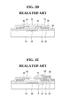
- FIGS. 1A to 1E are cross-sectional views showing a method of manufacturing a thin film transistor used for a related art active matrix display.
- a gate metal film is deposited on a substrate 10 and patterned to form a gate wiring (not shown) and a gate electrode 20 extending from the gate wiring.
- a gate insulating film 30, an amorphous silicon film 32, and an impurity-containing amorphous silicon film 34 are sequentially deposited over the entire surface of the substrate 10 with the gate electrode 20 formed thereon so as to cover the gate electrode 20.
- the amorphous silicon film 32 and the impurity-containing amorphous silicon film 34 are patterned to form an active layer 35.
- a data metal layer is deposited over the entire surface of the substrate 10 with the active layer 35 formed thereon.
- the data metal layer is patterned to form a data wiring (not shown) crossing the gate wiring, with the gate insulating film 30 interposed therebetween, and a source electrode 42 and a drain electrode 44 on the active layer 35 so as to partially overlap with the gate electrode 20 and face each other.
- an impurity-containing amorphous silicon pattern exposed between the source electrode 42 and the drain electrode 44 is etched using the source electrode 42 and the drain electrode 44 as a mask, thereby forming a channel Ch.
- a passivation film 50 is formed over the entire surface of the substrate 10 with the data wiring (not shown), the source electrode 42, and the drain electrode 44 formed thereon, and then a contact hole 52 is formed to expose a portion of the drain electrode 44 of the thin film transistor.
- the passivation film 50 is for protecting the channel Ch from external moisture or contact.
- a transparent metal layer is deposited on the passivation film 50 with the contact hole 52 formed therein, and then patterned to form a pixel electrode 60.
- the pixel electrode 60 is connected to the drain electrode 44 of the thin film transistor exposed through the contact hole 52 of the passivation film 50.
- FIG. 2 is an enlarged cross-sectional view showing portion A of FIG. 1e .
- the gate electrode 20, the source electrode 42, and the drain electrode 44 are protruded higher than their neighboring parts because they are formed by patterning. Accordingly, when the source electrode 42 and the pixel electrode 60 are formed thick to decrease electrical resistance, short-circuiting may occur because the step coverage of the gate insulating film 30, active layer 35, source electrode 42, and drain electrode 44 to be formed during a subsequent process increases because of the step difference with the gate electrode.
- the source electrode 42 and the drain electrode 44 are likewise formed thick to decrease electrical resistance, short-circuiting may occur because the step coverage of the passivation film 50 and the pixel electrode 60 to be formed during a subsequent process increases because of the step difference with the source electrode and the drain electrode.
- the parasitic capacitance Cp between the gate electrode 20 and the source and drain electrodes 42 and 44 may increase due to the step difference with the gate electrode 20. This may cause severe flickering on the display device and generate a picture quality defect.
- the present invention has been made in an effort to solve the problems occurring in the related art and to provide a method of forming a low-resistance wire, which increase aperture ratio by the use of a low-resistance material for thickening the wire, and improves picture quality by preventing the problems of step coverage caused by the increased wire thickness and flickering, and a method of manufacturing a thin film transistor using the same.
- a method of forming a wire comprising: depositing a metal layer on a base layer; exposing a portion of the base layer by removing a portion of the metal layer; forming grooves in the base layer by removing the exposed portion of the base layer by using the metal layer as a mask; forming a seed layer in the grooves of the base layer; and forming a wire consisting of the seed layer and a plated layer by plating a plating material on the seed layer formed in the grooves of the base layer by an electroless plating method or electroplating method.
- a method of forming a wire comprising: depositing an organic insulating film on a base layer; forming grooves or openings in the organic insulating film by removing a portion of the organic insulating film; forming a seed layer in the grooves or openings of the organic insulating film; and forming a wire consisting of the seed layer and a plated layer by plating a plating material on the seed layer formed in the grooves of the organic insulating layer by an electroless plating method or electroplating method.
- a method of forming a wire comprising: sequentially applying an organic insulating film and a metal layer on a base layer; exposing a portion of the organic insulating film by removing a portion of the metal layer; forming grooves in the organic insulating film by removing the exposed portion of the organic insulating film by using the metal layer as a mask; forming a seed layer in the grooves of the organic insulating film; and forming a wire consisting of the seed layer and a plated layer by plating a plating material on the seed layer formed in the grooves of the organic insulating film by an electroless plating method or electroplating method.
- the wire is a gate wiring including a gate electrode or a data wiring including a source electrode and a drain electrode.
- the base layer is formed of a glass material selected from boro-phosphor silicate glass (BPSG), undoped silicate glass (USG), and phosphor silicate glass (PSG), or a plastic material when forming the gate wiring, or formed of an inorganic insulating film selected from a silicon oxide film and a silicon nitride when forming the data wiring.
- BPSG boro-phosphor silicate glass
- USG undoped silicate glass
- PSG phosphor silicate glass
- the metal layer is formed of a material selected from the group consisting of Ti, a Ti-alloy, Al, and an Al-alloy.
- the seed layer is formed of a material selected from the group consisting of Pd, Pt, Au, Cu, Mo, Cr, and Ti
- the plated layer is formed of a material selected from the group consisting of AG, Au, and Cu.
- a method of manufacturing a thin film transistor comprising: forming a wire consisting of a seed layer and a plated layer as a gate electrode by using the method claimed in claim 1; sequentially depositing a gate insulating film, an amorphous silicon film, and an impurity-containing amorphous silicon film so as to cover the gate electrode, and patterning the amorphous silicon film and the impurity-containing amorphous silicon film to form a semiconductor layer; depositing a data metal layer over the entire surface of the substrate with the semiconductor layer formed thereon, and patterning the data metal layer to form a source electrode and a drain electrode on the semiconductor layer so as to face each other; and forming a channel by removing the impurity-containing amorphous silicon film exposed between the source electrode and the drain electrode by using the source electrode and the drain electrode as a mask.
- a method of manufacturing a thin film transistor comprising: forming a wire consisting of a seed layer and a plated layer as a gate electrode by using the method claimed in claim 1; sequentially depositing a gate insulating film, an amorphous silicon film, and an impurity-containing amorphous silicon film so as to cover the gate electrode, and patterning the amorphous silicon film and the impurity-containing amorphous silicon film to form a semiconductor layer; forming an organic insulating film on the gate insulating film over the entire surface of the substrate with the semiconductor layer formed thereon by using the method claimed in claim 2 or 3, forming grooves or through holes in the organic insulating film, and forming a data conductive layer consisting of a seed layer and a plated layer in the grooves or through holes; patterning the data conductive layer to form a source electrode and a drain electrode on the semiconductor layer so as to face each other; and forming a channel by removing the impurity-containing
- a method of manufacturing a thin film transistor comprising: forming a gate electrode on a base layer; sequentially depositing a gate insulating film, an amorphous silicon film, and an impurity-containing amorphous silicon film over the entire surface of the base layer with the gate electrode formed thereon so as to cover the gate electrode, and patterning the amorphous silicon film and the impurity-containing amorphous silicon film to form a semiconductor layer; forming an organic insulating film on the gate insulating film over the entire surface of the substrate with the semiconductor layer formed thereon by using the method claimed in claim 2 or 3, forming grooves or through holes in the organic insulating film, and forming a data conductive layer consisting of a seed layer and a plated layer in the grooves or through holes; patterning the data conductive layer to form a source electrode and a drain electrode on the semiconductor layer so as to face each other; and forming a channel by removing the impurity-containing a
- FIGS. 1A to 1E are cross-sectional views showing a method of manufacturing a thin film transistor used for a related art active matrix display
- FIG. 2 is an enlarged cross-sectional view showing portion A of FIG. 1E ;
- FIGS. 3A to 3F are cross-sectional views showing a process of forming a wire of a flat panel display according to a first exemplary embodiment of the present invention
- FIGS. 4A to 4G are cross-sectional views showing a process of forming a wire of a flat panel display according to a second exemplary embodiment of the present invention.
- FIGS. 5A to 5F are cross-sectional views showing a process of forming a wire of a flat panel display according to a third exemplary embodiment of the present invention.
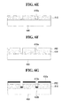
- FIGS. 6A to 6I are cross-sectional views showing a process of forming a wire of a flat panel display according to a fourth exemplary embodiment of the present invention.
- FIGS. 7A to 7E are cross-sectional views showing a process of manufacturing a thin film transistor by employing the process of forming a wire of a flat panel display according to the first or second exemplary embodiment of the present invention
- FIGS. 8A to 8F are cross-sectional views showing a process of manufacturing a thin film transistor by employing the process of forming a wire of a flat panel display according to the third or fourth exemplary embodiment of the present invention.
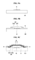
- FIGS. 9A to 9F are cross-sectional views showing a process of manufacturing a thin film transistor by employing the process of forming a wire of a flat panel display according to the third or fourth exemplary embodiment of the present invention.
- the wire to be formed in the first exemplary embodiment includes a gate wiring having a gate electrode and a data wiring comprising a source electrode and a gate electrode.
- a photoresist pattern PR1 is formed on a base layer 100 by a photolithography process so as to expose a portion of the base layer 100 under it.
- the base layer 100 is formed of a glass material, such as boro-phosphor silicate glass (BPSG), undoped silicate glass (USG), and phosphor silicate glass (PSG), or a plastic material when forming a gate wiring, or formed of an inorganic insulator film, such as a silicon oxide film and a silicon nitride when forming a data wiring.
- the base layer 100 exposed through the photoresist pattern PR1 is etched by dry etching using an etching gas to form grooves 101.
- a metal such as Pt, Au, Cu, Mo, Cr, and Ti is applied onto the base layer 100 with the grooves 101 and the photoresist pattern PR1 by physical vapor deposition (PVD) or chemical vapor deposition (CVD) so that a first conductive layer 110a and 110b is formed on the photoresist pattern PR1 and in the grooves 101 of the base layer 100.
- the first conductive layer 110a and 110b may be formed of a single layer or double layers. If the first conductive layer 110a and 110b is formed of double layers, a metal having good contactability with the base layer 100 is formed as a lower layer.
- the photoresist pattern PR1 with the first conductive layer 110a is removed so that the first conductive layer 110b formed in the grooves 101 of the base layer 100 remains, thereby forming a seed metal 110b.
- a plating metal 115 such as Ag, Au, and Cu, which are low-resistance metals, is plated on the seed metal 110b by a well-known electroplating method or electroless plating method, thereby forming a wire 120.
- the thickness of the wire 120 consisting of the seed metal 110b and the plating metal 115 is equal to or greater than the depth of the grooves 101 of the base layer 100, and may be properly selected as necessary.
- the wire to be formed in the second exemplary embodiment includes a gate wiring having a gate electrode and a data wiring having a source electrode and a gate electrode.
- the wire forming method of the second exemplary embodiment is different from the wire forming method of the first exemplary embodiment in that a first conductive layer is additionally formed prior to forming a photoresist pattern.
- a first conductive layer 210 made of Ti, an Ti-alloy, Al, and an Al-alloy is applied onto a base layer 200 by physical vapor deposition (PVD) or chemical vapor deposition (CVD).
- the base layer 200 is formed of a glass material, such as boro-phosphor silicate glass (BPSG), undoped silicate glass (USG), and phosphor silicate glass (PSG), or a plastic material when forming a gate wiring, or formed of an inorganic insulating film, such as a silicon oxide film and a silicon nitride when forming a data wiring.
- a photoresist pattern PR1 is formed on the base layer 200 with the first conductive layer 210 deposited thereon by a photolithography process so as to expose a portion of the first conductive layer 210. After that, the portion of the first conductive layer 210 exposed through the photoresist pattern PR1 is removed by wet etching using an etching solution, thereby forming a first conductive pattern 210a.
- the photoresist pattern PR1 and the portion of the base layer 200 exposed through the first conductive pattern 210a are etched by dry etching using an etching as, thereby forming grooves 201 in the base layer 200.
- a metal such as Pt, Au, Cu, Mo, Cr, and Ti is applied onto the base layer 200 with the grooves 201 formed therein and the photoresist pattern PR1 by physical vapor deposition (PVD) or chemical vapor deposition (CVD) to form a second conductive layer 220a and 220b on the photoresist pattern PR1 and in the grooves 201 of the base layer 200.
- PVD physical vapor deposition
- CVD chemical vapor deposition
- the photoresit pattern PR1 with the second conductive layer 220a is removed, and the second conductive layer 210a formed on the base layer 200 is selectively etched so that the second conductive layer 220b formed in the grooves 201 of the base layer 200 remains, thereby forming a seed metal 220b in the grooves 201 of the base layer 200.
- a plating metal 225 such as Ag, Au, and Cu, which are low-resistance metals, is plated on the seed metal 220b by a well-known electroplating method or electroless plating method, thereby forming a wire 230.
- the thickness of the wire 230 consisting of the seed metal 220b and the plating metal 225 is equal to or greater than the depth of the grooves 201 of the base layer 200, and may be properly selected as necessary.
- the first conductive layer 210a is formed on the base layer 200, and this prevents the top surface of the base layer 200 from being excessively etched when forming the grooves 201 in the base layer 200. Therefore, the shape of the grooves 201 to be formed on the base layer 200 can be controlled more finely, compared to the wire forming method of the first exemplary embodiment.
- the wire to be formed in the third exemplary embodiment comprises a gate wiring comprising a gate electrode and a data wiring comprising a source electrode and a gate electrode.
- the wire forming method of the third exemplary embodiment is different from the wire forming method of the first exemplary embodiment in that, after forming an organic insulating film with grooves (or through holes) on a baser layer, a wire is formed in the grooves of the organic insulating film.
- an organic insulating film 310 made of polyimide, photo acryl, etc is formed on a base layer 300.
- the base layer 300 is formed of a glass material, such as boro-phosphor silicate glass (BPSG), undoped silicate glass (USG), and phosphor silicate glass (PSG), or a plastic material when forming a gate wiring, or formed of an inorganic insulating film, such as a silicon oxide film and a silicon nitride when forming a data wiring.
- BPSG boro-phosphor silicate glass
- USG undoped silicate glass
- PSG phosphor silicate glass
- a photoresist pattern PR1 is formed on the base layer 300 with the organic insulating film 310 by a photolithography process so as to expose a portion of the organic insulating film 310. After that, the portion of the organic insulating film 310 exposed through the photoresist pattern Pr1 is removed by dry etching using an etching gas, thereby forming an organic insulating film pattern 310a having grooves or openings 310b.
- a metal such as Pt, Au, Cu, Mo, Cr, and Ti is applied onto the photoresist pattern PR1 having the grooves or openings 310b by physical vapor deposition (PVD) or chemical vapor deposition (CVD) to form a first conductive layer 320a and 320b on the photoresist pattern PR1 and in the grooves 310b of the organic insulating film 310a.
- PVD physical vapor deposition
- CVD chemical vapor deposition
- the photoresist pattern PR1 with the first conductive layer 320a is removed so that the first conductive layer 320b formed in the openings 310b of the organic insulating film pattern 310b remains, thereby forming a seed metal 320b.
- a plating metal 325 such as Ag, Au, and Cu, which are low-resistance metals, is plated on the seed metal 320b by a well-known electroplating method or electroless plating method, thereby forming a wire 330.
- the thickness of the wire 330 consisting of the seed metal 320b and the plating metal 325 is equal to or greater than the depth of the grooves or openings 310b of the organic insulating film pattern 310a, and may be properly selected as necessary.
- a wire is formed in the grooves or openings of the organic insulating film, and this gives the effect of reducing the step difference with electrodes of the display device to be formed in a process subsequent to the formation of a source electrode and a drain electrode.
- the wire to be formed in the fourth exemplary embodiment comprises a gate wiring comprising a gate electrode and a data wiring comprising a source electrode and a gate electrode.
- the wire forming method of the third exemplary embodiment is different from the wire forming method of the third exemplary embodiment in that a first conductive layer is formed after forming an organic insulating film on a base layer.
- an organic insulating film 410 made of polyimide, photo acryl, etc and a first conductive layer 420 are sequentially applied onto a base layer 400 by physical vapor deposition (PVD) or chemical vapor deposition (CVD).
- the base layer 400 is formed of a glass material, such as boro-phosphor silicate glass (BPSG), undoped silicate glass (USG), and phosphor silicate glass (PSG), or a plastic material when forming a gate wiring, or formed of an inorganic insulating film, such as a silicon oxide film and a silicon nitride when forming a data wiring.
- the first conductive layer 420 comprises Ti, a Ti-alloy, Al, and an Al-alloy.
- a first photoresist pattern PR1 is formed on the first conductive layer 420 by a photolithography process so as to expose a portion of the first conductive layer 420. After that, the portion of the first conductive layer 420 exposed through the first photoresist pattern PR1 is removed by wet etching using an etching solution, thereby forming a first conductive pattern 420a having openings 420b.
- the first photoresist pattern PR1 is removed, and the organic insulating film 410 is dryetched by using the first conductive pattern 420a as a mask, thereby forming grooves 410a in the organic insulating film 410.
- the first conductive pattern 420a formed on the organic insulating film 410 is selectively etched and removed to expose the organic insulating film 410.
- a second photoresist pattern PR2 having openings corresponding to the grooves 410a of the organic insulating film 410 is formed on the organic insulating film 410 with the grooves 410a by a photolithography process.
- a metal such as Pt, Au, Cu, Mo, Cr, and Ti is applied onto the organic insulating film 410 with the grooves 410a formed therein and the second photoresist pattern PR2 by physical vapor deposition (PVD) or chemical vapor deposition (CVD) to form a second conductive layer 430a and 430b on the photoresist pattern PR1 and in the grooves 410b of the base layer 400.
- PVD physical vapor deposition
- CVD chemical vapor deposition
- the second photoresist pattern PR2 with the second conductive layer 430a is removed so that the second conductive layer 430b formed in the openings 410b of the organic insulating film 410 remains, thereby forming a seed metal 430b.
- a plating metal 435 such as Ag, Au, and Cu, which are low-resistance metals, is plated on the seed metal 430b by a well-known electroplating method or electroless plating method, thereby forming a wire 440.
- the thickness of the wire 440 consisting of the seed metal 430b and the plating metal 435 is equal to or greater than the depth of the 410a of the organic insulating film 410, and may be properly selected as necessary.
- the grooves 410a are formed in the organic insulating film 410 after the first conductive pattern 420a is formed on top of the organic insulating film 410, and this prevents the top surface of the organic insulating film 410 from being excessively etched when forming the grooves 410a in the organic insulating film 410. Therefore, the shape of the grooves 410a to be formed on the organic insulating film 410 can be controlled more finely, compared to the wire forming method of the third exemplary embodiment.
- a wire can be formed in various combinations. That is, each of the wire forming methods of the first to fourth exemplary embodiments is applicable to a method of forming a gate wiring comprising a gate electrode and a method of forming a data wiring comprising a source electrode and a drain electrode, various combinations of these methods may be used. Therefore, although no description is given of each of the various combinations, it should be understood that the structure of a wire to be formed by the combinations of the fourth exemplary embodiment falls within the scope of the present invention.
- FIGS. 7A to 7E are cross-sectional views showing a process of manufacturing a thin film transistor by employing the wire forming methods of the first and second exemplary embodiments of the present invention in the forming of a gate wiring comprising a gate electrode.
- a gate electrode GE consisting of a seed metal S and a plating metal P is formed on a substrate SUB by the wire forming method of the first or second exemplary embodiment.
- the substrate SSB is formed of a glass material, such as boro-phosphor silicate glass (BPSG), undoped silicate glass (USG), and phosphor silicate glass (PSG), or a plastic material.
- BPSG boro-phosphor silicate glass
- USG undoped silicate glass
- PSG phosphor silicate glass
- a gate insulating film GI, an amorphous silicon film SEM1, and an impurity-containing amorphous silicon film SEM2 are sequentially deposited over the entire surface of the substrate SUB with the gate electrode GE formed thereon so as to cover the gate electrode GE.
- the amorphous silicon film SEM1 and the impurity-containing amorphous silicon film SEM2 are patterned to form a semiconductor layer SEM.
- a data conductive layer is deposited over the entire surface of the substrate SUB with the semiconductor layer SEM formed thereon.
- the data conductive layer is patterned to form a data wiring (not shown) crossing the gate wiring, with the gate insulating film GI interposed therebetween, and a source electrode SE and a drain electrode DE on the semiconductor layer SEM so as to partially overlap with the gate electrode GE and face each other.
- an impurity-containing amorphous silicon pattern exposed between the source electrode SE and the drain electrode DE is etched using the source electrode SE and the drain electrode DE as a mask, thereby forming a channel Ch.
- a passivation film PAS is formed over the entire surface of the substrate SUB with the data wiring (not shown), the source electrode SE, and the drain electrode DE formed thereon, and then a contact hole H is formed to expose a portion of the drain electrode DE of the thin film transistor.
- the passivation film PAS is for protecting the channel Ch from external moisture or contact.
- a transparent conductive layer is deposited on the passivation film PAS with the contact hole H formed therein, and then patterned to form an electrode EL.
- the electrode EL is connected to the drain electrode DE of the thin film transistor exposed through the contact hole H of the passivation film PAS.
- FIGS. 8A to 8F are cross-sectional views showing a process of manufacturing a thin film transistor by employing the wire forming method of the first or second exemplary embodiment of the present invention in the forming of a gate electrode and the wire forming method of the third or fourth exemplary embodiment in the forming of a source electrode and a drain electrode.
- the process steps of FIG. 8A and 8B in the process of FIGS. 8A to 8E are identical to those of FIGS. 7A and 7B , so a description thereof will be omitted.
- the process shown in FIGS. 5B to 5F of the third exemplary embodiment or the process shown in FIGS. 6B to 6i of the fourth exemplary embodiment is used to form an organic insulating film OI on a gate insulating film GI over the entire surface of a substrate SUB with a semiconductor layer SEM formed thereon, form grooves or through holes in the organic insulating film OI, and form a data metal layer DL consisting of a second seed metal S2 and a second plating metal PS in the grooves or through holes.
- the data metal layer DL is patterned by a photolithography process to form a data wiring (not shown) crossing a gate wiring, with the gate insulating film GI interposed therebetween, and a source electrode SE and a drain electrode DE on the semiconductor layer SEM so as to partially overlap with the gate electrode GE and face each other.
- an impurity-containing amorphous silicon film SEM2 exposed between the source electrode SE and the drain electrode DE is etched using the source electrode SE and the drain electrode DE as a mask, thereby forming a channel Ch.
- a passivation film PAS is formed over the entire surface of the substrate SUB with the data wiring (not shown), the source electrode SE, and the drain electrode DE formed thereon, and then a contact hole H is formed to expose a portion of the drain electrode DE of the thin film transistor.
- the passivation film PAS is for protecting the channel Ch from external moisture or contact.
- a transparent metal layer is deposited on the passivation film PAS with the contact hole H formed therein, and then patterned to form an electrode EL.
- the electrode EL is connected to the drain electrode DE of the thin film transistor exposed through the contact hole H of the passivation film PAS.
- FIGS. 9A to 9F are cross-sectional views showing a process of manufacturing a thin film transistor by employing the wire forming method of the related art in the forming of a gate electrode and the wire forming method of the third and fourth exemplary embodiments in the forming of a source electrode and a drain electrode.
- a gate metal film is deposited on a substrate SUB and patterned to form a gate wiring (not shown) and a gate electrode GE extending from the gate wiring.
- a gate insulating film GI, an amorphous silicon film SEM1, and an impurity-containing amorphous silicon film SEM2 are sequentially deposited over the entire surface of the substrate SUB with the gate electrode GE formed thereon so as to cover the gate electrode GE.
- the amorphous silicon film SEM1 and the impurity-containing amorphous silicon film SEM2 are patterned to form a semiconductor layer SEM.
- the process shown in FIGS. 5b to 5f of the third exemplary embodiment or the process shown in FIGS. 6b to 6i of the fourth exemplary embodiment is used to form an organic insulating film OI on a gate insulating film GI over the entire surface of a substrate SUB with a semiconductor layer SEM formed thereon, form grooves or through holes in the organic insulating film OI, and form a data metal layer DL consisting of a second seed metal S2 and a second plating metal PS in the grooves or through holes.
- the baser layer of the third and fourth exemplary embodiments consists of a gate insulating film and a semiconductor layer.
- the data metal layer DL is patterned by a photolithography process to form a data wiring (not shown) crossing a gate wiring, with the gate insulating film GI interposed therebetween, and a source electrode SE and a drain electrode DE on the semiconductor layer SEM so as to partially overlap with the gate electrode GE and face each other.
- an impurity-containing amorphous silicon film SEM2 exposed between the source electrode SE and the drain electrode DE is etched using the source electrode SE and the drain electrode DE as a mask, thereby forming a channel Ch.
- a passivation film PAS is formed over the entire surface of the substrate SUB with the data wiring (not shown), the source electrode SE, and the drain electrode DE formed thereon, and then a contact hole H is formed to expose a portion of the drain electrode DE of the thin film transistor.
- the passivation film PAS is for protecting the channel Ch from external moisture or contact.
- a transparent metal layer is deposited on the passivation film PAS with the contact hole H formed therein, and then patterned to form an electrode EL.
- the electrode EL is connected to the drain electrode DE of the thin film transistor exposed through the contact hole H of the passivation film PAS.
- grooves or openings are formed in a base layer to form a wire using a low-resistance metal. This may increase the thickness of the wire and hence increase aperture ratio, and this may overcome the problem of step coverage caused by the increased wire thickness. Therefore, the problems of short-circuiting and flickering can be prevented, thereby leading to picture quality improvement.
Landscapes
- Thin Film Transistor (AREA)
- Engineering & Computer Science (AREA)
- Manufacturing & Machinery (AREA)
- Internal Circuitry In Semiconductor Integrated Circuit Devices (AREA)
- Electrodes Of Semiconductors (AREA)
Abstract
Description
- This document relates to method of forming a low-resistance wire and a method of manufacturing a thin film transistor using the same, and more particularly, to a method of forming low-resistance metal gate and data wirings and a method of manufacturing a thin film transistor using the same.
- Various flat panel displays having reduced weight and volume when compared with a cathode ray tube have been developed. Flat panel displays (FPDs) include liquid crystal displays (LCD), field emission displays (FED), plasma display panels (PDP), organic light emitting diode (OLED) displays, and the like.
- Out of the flat panel displays, the application range of the liquid crystal displays has widened because the liquid crystal display can be manufactured to be lightweight and thin and can be driven under low power consumption. Moreover, the OLED displays have a fast response time equal to or less than about 1 ms, low power consumption, and a wide viewing angle by a self light emitting. Thus, the OLED displays have been considered as a next generation display.
- The liquid crystal displays and the OLED displays are driven by a passive matrix method or an active matrix method using a thin film transistor. The active matrix method, in which a thin film transistor and a pixel electrode connected to the thin film transistor are arranged in a matrix, are attracting considerable attention due to its high resolution and superior moving picture reproducing capability.
- An active matrix display using a thin film transistor supplies signals to each pixel through gate wirings for supplying scan signals and data wirings for supplying data signals, and supplies power to each pixel through power lines for supplying power.
- For a large-sized display device of more than 18 inches having a high resolution, the material used for the gate and data wirings becomes a highly important factor for determining picture quality because the picture quality depends on the specific resistance of the material. The resistance of the entire lines including the gate wirings and the data wirings increases with the trend of large-sized and high-resolution displays. This increases the resistance of each line and the parasitic capacitance between the lines, thus leading to an RC delay caused by resistance-capacitance. Moreover, crosstalk occurs due to the RC-delay, thereby deteriorating picture quality.
- Therefore, low-resistance metals such as aluminum or aluminum alloys may be used for the gate wirings and the data wirings in order to prevent such an RC-delay. However, aluminum has poor chemical corrosion resistance, and may cause a defect in a subsequent process.
- To solve this problem, the line width or the line thickness may be increased to reduce resistance. However, increasing the line thickness may increase the risk of short-circuiting due to a large step coverage.
- Hereinafter, the above-described problem will be explained in more detail with reference to
FIGS. 1a to 1e. FIGS. 1A to 1E are cross-sectional views showing a method of manufacturing a thin film transistor used for a related art active matrix display. - Referring to
FIG. 1A , a gate metal film is deposited on asubstrate 10 and patterned to form a gate wiring (not shown) and agate electrode 20 extending from the gate wiring. - Referring to
FIG. 1B , a gateinsulating film 30, anamorphous silicon film 32, and an impurity-containingamorphous silicon film 34 are sequentially deposited over the entire surface of thesubstrate 10 with thegate electrode 20 formed thereon so as to cover thegate electrode 20. Theamorphous silicon film 32 and the impurity-containingamorphous silicon film 34 are patterned to form anactive layer 35. - Referring to
FIG. 1C , a data metal layer is deposited over the entire surface of thesubstrate 10 with theactive layer 35 formed thereon. The data metal layer is patterned to form a data wiring (not shown) crossing the gate wiring, with thegate insulating film 30 interposed therebetween, and asource electrode 42 and adrain electrode 44 on theactive layer 35 so as to partially overlap with thegate electrode 20 and face each other. Next, an impurity-containing amorphous silicon pattern exposed between thesource electrode 42 and thedrain electrode 44 is etched using thesource electrode 42 and thedrain electrode 44 as a mask, thereby forming a channel Ch. - Referring to
FIG. 1D , apassivation film 50 is formed over the entire surface of thesubstrate 10 with the data wiring (not shown), thesource electrode 42, and thedrain electrode 44 formed thereon, and then acontact hole 52 is formed to expose a portion of thedrain electrode 44 of the thin film transistor. Thepassivation film 50 is for protecting the channel Ch from external moisture or contact. - Referring to
FIG. 1E , a transparent metal layer is deposited on thepassivation film 50 with thecontact hole 52 formed therein, and then patterned to form apixel electrode 60. Thepixel electrode 60 is connected to thedrain electrode 44 of the thin film transistor exposed through thecontact hole 52 of thepassivation film 50. -
FIG. 2 is an enlarged cross-sectional view showing portion A ofFIG. 1e . Referring toFIG. 2 , thegate electrode 20, thesource electrode 42, and thedrain electrode 44 are protruded higher than their neighboring parts because they are formed by patterning. Accordingly, when thesource electrode 42 and thepixel electrode 60 are formed thick to decrease electrical resistance, short-circuiting may occur because the step coverage of thegate insulating film 30,active layer 35,source electrode 42, anddrain electrode 44 to be formed during a subsequent process increases because of the step difference with the gate electrode. Also, when thesource electrode 42 and thedrain electrode 44 are likewise formed thick to decrease electrical resistance, short-circuiting may occur because the step coverage of thepassivation film 50 and thepixel electrode 60 to be formed during a subsequent process increases because of the step difference with the source electrode and the drain electrode. - Moreover, as shown in
FIG. 2 , the parasitic capacitance Cp between thegate electrode 20 and the source anddrain electrodes gate electrode 20. This may cause severe flickering on the display device and generate a picture quality defect. - Accordingly, the present invention has been made in an effort to solve the problems occurring in the related art and to provide a method of forming a low-resistance wire, which increase aperture ratio by the use of a low-resistance material for thickening the wire, and improves picture quality by preventing the problems of step coverage caused by the increased wire thickness and flickering, and a method of manufacturing a thin film transistor using the same.
- According to an embodiment, there is provided a method of forming a wire, the method comprising: depositing a metal layer on a base layer; exposing a portion of the base layer by removing a portion of the metal layer; forming grooves in the base layer by removing the exposed portion of the base layer by using the metal layer as a mask; forming a seed layer in the grooves of the base layer; and forming a wire consisting of the seed layer and a plated layer by plating a plating material on the seed layer formed in the grooves of the base layer by an electroless plating method or electroplating method.
- According to another embodiment, there is provided a method of forming a wire, the method comprising: depositing an organic insulating film on a base layer; forming grooves or openings in the organic insulating film by removing a portion of the organic insulating film; forming a seed layer in the grooves or openings of the organic insulating film; and forming a wire consisting of the seed layer and a plated layer by plating a plating material on the seed layer formed in the grooves of the organic insulating layer by an electroless plating method or electroplating method.
- According to a further another embodiment, there is provided a method of forming a wire, the method comprising: sequentially applying an organic insulating film and a metal layer on a base layer; exposing a portion of the organic insulating film by removing a portion of the metal layer; forming grooves in the organic insulating film by removing the exposed portion of the organic insulating film by using the metal layer as a mask; forming a seed layer in the grooves of the organic insulating film; and forming a wire consisting of the seed layer and a plated layer by plating a plating material on the seed layer formed in the grooves of the organic insulating film by an electroless plating method or electroplating method.
- Also, the wire is a gate wiring including a gate electrode or a data wiring including a source electrode and a drain electrode.
- Also, the base layer is formed of a glass material selected from boro-phosphor silicate glass (BPSG), undoped silicate glass (USG), and phosphor silicate glass (PSG), or a plastic material when forming the gate wiring, or formed of an inorganic insulating film selected from a silicon oxide film and a silicon nitride when forming the data wiring.
- Also, the metal layer is formed of a material selected from the group consisting of Ti, a Ti-alloy, Al, and an Al-alloy.
- Also, the seed layer is formed of a material selected from the group consisting of Pd, Pt, Au, Cu, Mo, Cr, and Ti, and the plated layer is formed of a material selected from the group consisting of AG, Au, and Cu.
- According to an another embodiment, there is provided a method of manufacturing a thin film transistor, the method comprising: forming a wire consisting of a seed layer and a plated layer as a gate electrode by using the method claimed in
claim 1; sequentially depositing a gate insulating film, an amorphous silicon film, and an impurity-containing amorphous silicon film so as to cover the gate electrode, and patterning the amorphous silicon film and the impurity-containing amorphous silicon film to form a semiconductor layer; depositing a data metal layer over the entire surface of the substrate with the semiconductor layer formed thereon, and patterning the data metal layer to form a source electrode and a drain electrode on the semiconductor layer so as to face each other; and forming a channel by removing the impurity-containing amorphous silicon film exposed between the source electrode and the drain electrode by using the source electrode and the drain electrode as a mask. - According to another embodiment, there is provided a method of manufacturing a thin film transistor, the method comprising: forming a wire consisting of a seed layer and a plated layer as a gate electrode by using the method claimed in
claim 1; sequentially depositing a gate insulating film, an amorphous silicon film, and an impurity-containing amorphous silicon film so as to cover the gate electrode, and patterning the amorphous silicon film and the impurity-containing amorphous silicon film to form a semiconductor layer; forming an organic insulating film on the gate insulating film over the entire surface of the substrate with the semiconductor layer formed thereon by using the method claimed inclaim 2 or 3, forming grooves or through holes in the organic insulating film, and forming a data conductive layer consisting of a seed layer and a plated layer in the grooves or through holes; patterning the data conductive layer to form a source electrode and a drain electrode on the semiconductor layer so as to face each other; and forming a channel by removing the impurity-containing amorphous silicon film exposed between the source electrode and the drain electrode by using the source electrode and the drain electrode as a mask. - According to a further another embodiment, there is provided a method of manufacturing a thin film transistor, the method comprising: forming a gate electrode on a base layer; sequentially depositing a gate insulating film, an amorphous silicon film, and an impurity-containing amorphous silicon film over the entire surface of the base layer with the gate electrode formed thereon so as to cover the gate electrode, and patterning the amorphous silicon film and the impurity-containing amorphous silicon film to form a semiconductor layer; forming an organic insulating film on the gate insulating film over the entire surface of the substrate with the semiconductor layer formed thereon by using the method claimed in
claim 2 or 3, forming grooves or through holes in the organic insulating film, and forming a data conductive layer consisting of a seed layer and a plated layer in the grooves or through holes; patterning the data conductive layer to form a source electrode and a drain electrode on the semiconductor layer so as to face each other; and forming a channel by removing the impurity-containing amorphous silicon film exposed between the source electrode and the drain electrode by using the source electrode and the drain electrode as a mask. - The accompanying drawings, which are included to provide a further understanding of the invention and are incorporated in and constitute a part of this specification, illustrate embodiments of the invention and together with the description serve to explain the principles of the invention. In the drawings:
-
FIGS. 1A to 1E are cross-sectional views showing a method of manufacturing a thin film transistor used for a related art active matrix display; -
FIG. 2 is an enlarged cross-sectional view showing portion A ofFIG. 1E ; -
FIGS. 3A to 3F are cross-sectional views showing a process of forming a wire of a flat panel display according to a first exemplary embodiment of the present invention; -
FIGS. 4A to 4G are cross-sectional views showing a process of forming a wire of a flat panel display according to a second exemplary embodiment of the present invention; -
FIGS. 5A to 5F are cross-sectional views showing a process of forming a wire of a flat panel display according to a third exemplary embodiment of the present invention; -
FIGS. 6A to 6I are cross-sectional views showing a process of forming a wire of a flat panel display according to a fourth exemplary embodiment of the present invention; -
FIGS. 7A to 7E are cross-sectional views showing a process of manufacturing a thin film transistor by employing the process of forming a wire of a flat panel display according to the first or second exemplary embodiment of the present invention; -
FIGS. 8A to 8F are cross-sectional views showing a process of manufacturing a thin film transistor by employing the process of forming a wire of a flat panel display according to the third or fourth exemplary embodiment of the present invention; and -
FIGS. 9A to 9F are cross-sectional views showing a process of manufacturing a thin film transistor by employing the process of forming a wire of a flat panel display according to the third or fourth exemplary embodiment of the present invention. - Hereinafter, exemplary embodiments of the present invention will be described in detail with reference to the accompanying drawings. Like reference numerals designate substantially like elements throughout the specification.
- First of all, a method of forming a wire of a flat panel display according to a first exemplary embodiment of the present invention will be described with reference to
FIGS. 3A to 3F . The wire to be formed in the first exemplary embodiment includes a gate wiring having a gate electrode and a data wiring comprising a source electrode and a gate electrode. - Referring to
FIGS. 3A and 3B , a photoresist pattern PR1 is formed on abase layer 100 by a photolithography process so as to expose a portion of thebase layer 100 under it. Thebase layer 100 is formed of a glass material, such as boro-phosphor silicate glass (BPSG), undoped silicate glass (USG), and phosphor silicate glass (PSG), or a plastic material when forming a gate wiring, or formed of an inorganic insulator film, such as a silicon oxide film and a silicon nitride when forming a data wiring. - Referring to
FIG. 3C , thebase layer 100 exposed through the photoresist pattern PR1 is etched by dry etching using an etching gas to formgrooves 101. - Referring to
FIG. 3D , a metal such as Pt, Au, Cu, Mo, Cr, and Ti is applied onto thebase layer 100 with thegrooves 101 and the photoresist pattern PR1 by physical vapor deposition (PVD) or chemical vapor deposition (CVD) so that a firstconductive layer grooves 101 of thebase layer 100. The firstconductive layer conductive layer base layer 100 is formed as a lower layer. - Referring to
FIG. 3E , the photoresist pattern PR1 with the firstconductive layer 110a is removed so that the firstconductive layer 110b formed in thegrooves 101 of thebase layer 100 remains, thereby forming aseed metal 110b. - Referring to
FIG. 3F , aplating metal 115, such as Ag, Au, and Cu, which are low-resistance metals, is plated on theseed metal 110b by a well-known electroplating method or electroless plating method, thereby forming awire 120. The thickness of thewire 120 consisting of theseed metal 110b and theplating metal 115 is equal to or greater than the depth of thegrooves 101 of thebase layer 100, and may be properly selected as necessary. - Next, a method of forming a wire of a flat panel display according to a second exemplary embodiment of the present invention will be described with reference to
FIGS. 4A to 4F . Like the wire to be formed in the first exemplary embodiment, the wire to be formed in the second exemplary embodiment includes a gate wiring having a gate electrode and a data wiring having a source electrode and a gate electrode. The wire forming method of the second exemplary embodiment is different from the wire forming method of the first exemplary embodiment in that a first conductive layer is additionally formed prior to forming a photoresist pattern. - Referring to
FIGS. 4A and 4B , a firstconductive layer 210 made of Ti, an Ti-alloy, Al, and an Al-alloy is applied onto abase layer 200 by physical vapor deposition (PVD) or chemical vapor deposition (CVD). Thebase layer 200 is formed of a glass material, such as boro-phosphor silicate glass (BPSG), undoped silicate glass (USG), and phosphor silicate glass (PSG), or a plastic material when forming a gate wiring, or formed of an inorganic insulating film, such as a silicon oxide film and a silicon nitride when forming a data wiring. - Referring to
FIG. 4C , a photoresist pattern PR1 is formed on thebase layer 200 with the firstconductive layer 210 deposited thereon by a photolithography process so as to expose a portion of the firstconductive layer 210. After that, the portion of the firstconductive layer 210 exposed through the photoresist pattern PR1 is removed by wet etching using an etching solution, thereby forming a firstconductive pattern 210a. - Referring to
FIG. 4D , the photoresist pattern PR1 and the portion of thebase layer 200 exposed through the firstconductive pattern 210a are etched by dry etching using an etching as, thereby forminggrooves 201 in thebase layer 200. - Referring to
FIG. 4E , a metal such as Pt, Au, Cu, Mo, Cr, and Ti is applied onto thebase layer 200 with thegrooves 201 formed therein and the photoresist pattern PR1 by physical vapor deposition (PVD) or chemical vapor deposition (CVD) to form a secondconductive layer grooves 201 of thebase layer 200. - Referring to
FIG. 4F , the photoresit pattern PR1 with the secondconductive layer 220a is removed, and the secondconductive layer 210a formed on thebase layer 200 is selectively etched so that the secondconductive layer 220b formed in thegrooves 201 of thebase layer 200 remains, thereby forming aseed metal 220b in thegrooves 201 of thebase layer 200. - Referring to
FIG. 4G , aplating metal 225, such as Ag, Au, and Cu, which are low-resistance metals, is plated on theseed metal 220b by a well-known electroplating method or electroless plating method, thereby forming awire 230. The thickness of thewire 230 consisting of theseed metal 220b and theplating metal 225 is equal to or greater than the depth of thegrooves 201 of thebase layer 200, and may be properly selected as necessary. - According to the wire forming method of the second exemplary embodiment, the first
conductive layer 210a is formed on thebase layer 200, and this prevents the top surface of thebase layer 200 from being excessively etched when forming thegrooves 201 in thebase layer 200. Therefore, the shape of thegrooves 201 to be formed on thebase layer 200 can be controlled more finely, compared to the wire forming method of the first exemplary embodiment. - Next, a method of forming a wire of a flat panel display according to a third exemplary embodiment of the present invention will be described with reference to
FIGS. 5A to 5F . Like the wire to be formed in the first and second exemplary embodiments, the wire to be formed in the third exemplary embodiment comprises a gate wiring comprising a gate electrode and a data wiring comprising a source electrode and a gate electrode. The wire forming method of the third exemplary embodiment is different from the wire forming method of the first exemplary embodiment in that, after forming an organic insulating film with grooves (or through holes) on a baser layer, a wire is formed in the grooves of the organic insulating film. - Referring to
FIGS. 5A and 5B , an organicinsulating film 310 made of polyimide, photo acryl, etc is formed on abase layer 300. Thebase layer 300 is formed of a glass material, such as boro-phosphor silicate glass (BPSG), undoped silicate glass (USG), and phosphor silicate glass (PSG), or a plastic material when forming a gate wiring, or formed of an inorganic insulating film, such as a silicon oxide film and a silicon nitride when forming a data wiring. - Referring to
FIG. 5C , a photoresist pattern PR1 is formed on thebase layer 300 with the organic insulatingfilm 310 by a photolithography process so as to expose a portion of the organic insulatingfilm 310. After that, the portion of the organic insulatingfilm 310 exposed through the photoresist pattern Pr1 is removed by dry etching using an etching gas, thereby forming an organic insulatingfilm pattern 310a having grooves oropenings 310b. - Referring to
FIG. 5D , a metal such as Pt, Au, Cu, Mo, Cr, and Ti is applied onto the photoresist pattern PR1 having the grooves oropenings 310b by physical vapor deposition (PVD) or chemical vapor deposition (CVD) to form a firstconductive layer grooves 310b of the organic insulatingfilm 310a. - Referring to
FIG. 5E , the photoresist pattern PR1 with the firstconductive layer 320a is removed so that the firstconductive layer 320b formed in theopenings 310b of the organic insulatingfilm pattern 310b remains, thereby forming aseed metal 320b. - Referring to
FIG. 5F , aplating metal 325, such as Ag, Au, and Cu, which are low-resistance metals, is plated on theseed metal 320b by a well-known electroplating method or electroless plating method, thereby forming awire 330. The thickness of thewire 330 consisting of theseed metal 320b and theplating metal 325 is equal to or greater than the depth of the grooves oropenings 310b of the organic insulatingfilm pattern 310a, and may be properly selected as necessary. - According to the wire forming method of the third exemplary embodiment, a wire is formed in the grooves or openings of the organic insulating film, and this gives the effect of reducing the step difference with electrodes of the display device to be formed in a process subsequent to the formation of a source electrode and a drain electrode.
- Next, a method of forming a wire of a flat panel display according to a fourth exemplary embodiment of the present invention will be described with reference to
FIGS. 6A to 6I . Like the wire to be formed in the first to third exemplary embodiments, the wire to be formed in the fourth exemplary embodiment comprises a gate wiring comprising a gate electrode and a data wiring comprising a source electrode and a gate electrode. The wire forming method of the third exemplary embodiment is different from the wire forming method of the third exemplary embodiment in that a first conductive layer is formed after forming an organic insulating film on a base layer. - Referring to
FIGS. 6A and 6B , an organicinsulating film 410 made of polyimide, photo acryl, etc and a firstconductive layer 420 are sequentially applied onto abase layer 400 by physical vapor deposition (PVD) or chemical vapor deposition (CVD). Thebase layer 400 is formed of a glass material, such as boro-phosphor silicate glass (BPSG), undoped silicate glass (USG), and phosphor silicate glass (PSG), or a plastic material when forming a gate wiring, or formed of an inorganic insulating film, such as a silicon oxide film and a silicon nitride when forming a data wiring. The firstconductive layer 420 comprises Ti, a Ti-alloy, Al, and an Al-alloy. - Referring to
FIG. 6C , a first photoresist pattern PR1 is formed on the firstconductive layer 420 by a photolithography process so as to expose a portion of the firstconductive layer 420. After that, the portion of the firstconductive layer 420 exposed through the first photoresist pattern PR1 is removed by wet etching using an etching solution, thereby forming a firstconductive pattern 420a havingopenings 420b. - Referring to
FIG. 6D , the first photoresist pattern PR1 is removed, and the organic insulatingfilm 410 is dryetched by using the firstconductive pattern 420a as a mask, thereby forminggrooves 410a in the organic insulatingfilm 410. - Referring to
FIG. 6E , the firstconductive pattern 420a formed on the organic insulatingfilm 410 is selectively etched and removed to expose the organic insulatingfilm 410. - Referring to
FIG. 6F , a second photoresist pattern PR2 having openings corresponding to thegrooves 410a of the organic insulatingfilm 410 is formed on the organic insulatingfilm 410 with thegrooves 410a by a photolithography process. - Referring to
FIG. 6G , a metal such as Pt, Au, Cu, Mo, Cr, and Ti is applied onto the organic insulatingfilm 410 with thegrooves 410a formed therein and the second photoresist pattern PR2 by physical vapor deposition (PVD) or chemical vapor deposition (CVD) to form a secondconductive layer base layer 400. - Referring to
FIG. 6H , the second photoresist pattern PR2 with the secondconductive layer 430a is removed so that the secondconductive layer 430b formed in the openings 410b of the organic insulatingfilm 410 remains, thereby forming aseed metal 430b. - Referring to
FIG. 6I , aplating metal 435, such as Ag, Au, and Cu, which are low-resistance metals, is plated on theseed metal 430b by a well-known electroplating method or electroless plating method, thereby forming awire 440. The thickness of thewire 440 consisting of theseed metal 430b and theplating metal 435 is equal to or greater than the depth of the 410a of the organic insulatingfilm 410, and may be properly selected as necessary. - According to the wire forming method of the fourth exemplary embodiment, the
grooves 410a are formed in the organic insulatingfilm 410 after the firstconductive pattern 420a is formed on top of the organic insulatingfilm 410, and this prevents the top surface of the organic insulatingfilm 410 from being excessively etched when forming thegrooves 410a in the organic insulatingfilm 410. Therefore, the shape of thegrooves 410a to be formed on the organic insulatingfilm 410 can be controlled more finely, compared to the wire forming method of the third exemplary embodiment. - According to the above-described wire forming methods of the first to fourth exemplary embodiments, a wire can be formed in various combinations. That is, each of the wire forming methods of the first to fourth exemplary embodiments is applicable to a method of forming a gate wiring comprising a gate electrode and a method of forming a data wiring comprising a source electrode and a drain electrode, various combinations of these methods may be used. Therefore, although no description is given of each of the various combinations, it should be understood that the structure of a wire to be formed by the combinations of the fourth exemplary embodiment falls within the scope of the present invention.
- Next, a method of forming a thin film transistor for a display device by using the wire forming methods of the first and second exemplary embodiments of the present invention will be described.
-
FIGS. 7A to 7E are cross-sectional views showing a process of manufacturing a thin film transistor by employing the wire forming methods of the first and second exemplary embodiments of the present invention in the forming of a gate wiring comprising a gate electrode. - Referring to
FIG. 7A , a gate electrode GE consisting of a seed metal S and a plating metal P is formed on a substrate SUB by the wire forming method of the first or second exemplary embodiment. The substrate SSB is formed of a glass material, such as boro-phosphor silicate glass (BPSG), undoped silicate glass (USG), and phosphor silicate glass (PSG), or a plastic material. - Referring to
FIG. 7B , a gate insulating film GI, an amorphous silicon film SEM1, and an impurity-containing amorphous silicon film SEM2 are sequentially deposited over the entire surface of the substrate SUB with the gate electrode GE formed thereon so as to cover the gate electrode GE. The amorphous silicon film SEM1 and the impurity-containing amorphous silicon film SEM2 are patterned to form a semiconductor layer SEM. - Referring to
FIG. 7C , a data conductive layer is deposited over the entire surface of the substrate SUB with the semiconductor layer SEM formed thereon. The data conductive layer is patterned to form a data wiring (not shown) crossing the gate wiring, with the gate insulating film GI interposed therebetween, and a source electrode SE and a drain electrode DE on the semiconductor layer SEM so as to partially overlap with the gate electrode GE and face each other. Next, an impurity-containing amorphous silicon pattern exposed between the source electrode SE and the drain electrode DE is etched using the source electrode SE and the drain electrode DE as a mask, thereby forming a channel Ch. - Referring to
FIG.7D , a passivation film PAS is formed over the entire surface of the substrate SUB with the data wiring (not shown), the source electrode SE, and the drain electrode DE formed thereon, and then a contact hole H is formed to expose a portion of the drain electrode DE of the thin film transistor. The passivation film PAS is for protecting the channel Ch from external moisture or contact. - Referring to
FIG. 7E , a transparent conductive layer is deposited on the passivation film PAS with the contact hole H formed therein, and then patterned to form an electrode EL. The electrode EL is connected to the drain electrode DE of the thin film transistor exposed through the contact hole H of the passivation film PAS. -
FIGS. 8A to 8F are cross-sectional views showing a process of manufacturing a thin film transistor by employing the wire forming method of the first or second exemplary embodiment of the present invention in the forming of a gate electrode and the wire forming method of the third or fourth exemplary embodiment in the forming of a source electrode and a drain electrode. The process steps ofFIG. 8A and 8B in the process ofFIGS. 8A to 8E are identical to those ofFIGS. 7A and 7B , so a description thereof will be omitted. - Referring to
FIG. 8C , the process shown inFIGS. 5B to 5F of the third exemplary embodiment or the process shown inFIGS. 6B to 6i of the fourth exemplary embodiment is used to form an organic insulating film OI on a gate insulating film GI over the entire surface of a substrate SUB with a semiconductor layer SEM formed thereon, form grooves or through holes in the organic insulating film OI, and form a data metal layer DL consisting of a second seed metal S2 and a second plating metal PS in the grooves or through holes. - Referring to
FIG. 8D , the data metal layer DL is patterned by a photolithography process to form a data wiring (not shown) crossing a gate wiring, with the gate insulating film GI interposed therebetween, and a source electrode SE and a drain electrode DE on the semiconductor layer SEM so as to partially overlap with the gate electrode GE and face each other. Next, an impurity-containing amorphous silicon film SEM2 exposed between the source electrode SE and the drain electrode DE is etched using the source electrode SE and the drain electrode DE as a mask, thereby forming a channel Ch. - Referring to
FIG. 8E , a passivation film PAS is formed over the entire surface of the substrate SUB with the data wiring (not shown), the source electrode SE, and the drain electrode DE formed thereon, and then a contact hole H is formed to expose a portion of the drain electrode DE of the thin film transistor. The passivation film PAS is for protecting the channel Ch from external moisture or contact. - Referring to
FIG. 8F , a transparent metal layer is deposited on the passivation film PAS with the contact hole H formed therein, and then patterned to form an electrode EL. The electrode EL is connected to the drain electrode DE of the thin film transistor exposed through the contact hole H of the passivation film PAS. -
FIGS. 9A to 9F are cross-sectional views showing a process of manufacturing a thin film transistor by employing the wire forming method of the related art in the forming of a gate electrode and the wire forming method of the third and fourth exemplary embodiments in the forming of a source electrode and a drain electrode. - Referring to
FIG. 9A , a gate metal film is deposited on a substrate SUB and patterned to form a gate wiring (not shown) and a gate electrode GE extending from the gate wiring. - Referring to
FIG. 9B , a gate insulating film GI, an amorphous silicon film SEM1, and an impurity-containing amorphous silicon film SEM2 are sequentially deposited over the entire surface of the substrate SUB with the gate electrode GE formed thereon so as to cover the gate electrode GE. The amorphous silicon film SEM1 and the impurity-containing amorphous silicon film SEM2 are patterned to form a semiconductor layer SEM. - Referring to
FIG. 9C , the process shown inFIGS. 5b to 5f of the third exemplary embodiment or the process shown inFIGS. 6b to 6i of the fourth exemplary embodiment is used to form an organic insulating film OI on a gate insulating film GI over the entire surface of a substrate SUB with a semiconductor layer SEM formed thereon, form grooves or through holes in the organic insulating film OI, and form a data metal layer DL consisting of a second seed metal S2 and a second plating metal PS in the grooves or through holes. The baser layer of the third and fourth exemplary embodiments consists of a gate insulating film and a semiconductor layer. - Referring to
FIG. 9D , the data metal layer DL is patterned by a photolithography process to form a data wiring (not shown) crossing a gate wiring, with the gate insulating film GI interposed therebetween, and a source electrode SE and a drain electrode DE on the semiconductor layer SEM so as to partially overlap with the gate electrode GE and face each other. Next, an impurity-containing amorphous silicon film SEM2 exposed between the source electrode SE and the drain electrode DE is etched using the source electrode SE and the drain electrode DE as a mask, thereby forming a channel Ch. - Referring to
FIG. 9E , a passivation film PAS is formed over the entire surface of the substrate SUB with the data wiring (not shown), the source electrode SE, and the drain electrode DE formed thereon, and then a contact hole H is formed to expose a portion of the drain electrode DE of the thin film transistor. The passivation film PAS is for protecting the channel Ch from external moisture or contact. - Referring to
FIG. 9F , a transparent metal layer is deposited on the passivation film PAS with the contact hole H formed therein, and then patterned to form an electrode EL. The electrode EL is connected to the drain electrode DE of the thin film transistor exposed through the contact hole H of the passivation film PAS. - According to the above-described method of forming a wire and above-described method of manufacturing a thin film transistor using the same according the exemplary embodiments of the present invention, grooves or openings are formed in a base layer to form a wire using a low-resistance metal. This may increase the thickness of the wire and hence increase aperture ratio, and this may overcome the problem of step coverage caused by the increased wire thickness. Therefore, the problems of short-circuiting and flickering can be prevented, thereby leading to picture quality improvement.
- Throughout the description, it should be understood for those skilled in the art that various changes and modifications are possible without departing from the technical principles of the present invention. Therefore, the technical scope of the present invention is not limited to those detailed descriptions in this document but should be defined by the scope of the appended claims.
-
- 1. A method of forming a wire, the method comprising:
- depositing a metal layer on a base layer;
- exposing a portion of the base layer by removing a portion of the metal layer;
- forming grooves in the base layer by removing the exposed portion of the base layer by using the metal layer as a mask;
- forming a seed layer in the grooves of the base layer; and
- forming a wire consisting of the seed layer and a plated layer by plating a plating material on the seed layer formed in the grooves of the base layer by an electroless plating method or electroplating method.
- 2. A method of forming a wire, the method comprising:
- depositing an organic insulating film on a base layer;
- forming grooves or openings in the organic insulating film by removing a portion of the organic insulating film;
- forming a seed layer in the grooves or openings of the organic insulating film; and
- forming a wire consisting of the seed layer and a plated layer by plating a plating material on the seed layer formed in the grooves of the organic insulating layer by an electroless plating method or electroplating method.
- 3. A method of forming a wire, the method comprising:
- sequentially applying an organic insulating film and a metal layer on a base layer;
- exposing a portion of the organic insulating film by removing a portion of the metal layer;
- forming grooves in the organic insulating film by removing the exposed portion of the organic insulating film by using the metal layer as a mask;
- forming a seed layer in the grooves of the organic insulating film; and
- forming a wire consisting of the seed layer and a plated layer by plating a plating material on the seed layer formed in the grooves of the organic insulating film by an electroless plating method or electroplating method.
- 4. The method of any one of examples 1 to 3, wherein the wire is a gate wiring including a gate electrode or a data wiring including a source electrode and a drain electrode.
- 5. The method of example 4, wherein the base layer is formed of a glass material selected from boro-phosphor silicate glass (BPSG), undoped silicate glass (USG), and phosphor silicate glass (PSG), or a plastic material when forming the gate wiring, or formed of an inorganic insulating film selected from a silicon oxide film and a silicon nitride when forming the data wiring.
- 6. The method of example 1 or 3, wherein the metal layer is formed of a material selected from the group consisting of Ti, a Ti-alloy, Al, and an Al-alloy.
- 7. The method of any one of examples 1 to 3, wherein the seed layer is formed of a material selected from the group consisting of Pd, Pt, Au, Cu, Mo, Cr, and Ti, and the plated layer is formed of a material selected from the group consisting of AG, Au, and Cu.
- 8. A method of manufacturing a thin film transistor, the method comprising:
- forming a wire consisting of a seed layer and a plated layer as a gate electrode by using the method claimed in example 1;
- sequentially depositing a gate insulating film, an amorphous silicon film, and an impurity-containing amorphous silicon film so as to cover the gate electrode, and patterning the amorphous silicon film and the impurity-containing amorphous silicon film to form a semiconductor layer;
- depositing a data metal layer over the entire surface of the substrate with the semiconductor layer formed thereon, and patterning the data metal layer to form a source electrode and a drain electrode on the semiconductor layer so as to face each other; and
- forming a channel by removing the impurity-containing amorphous silicon film exposed between the source electrode and the drain electrode by using the source electrode and the drain electrode as a mask.
- 9. A method of manufacturing a thin film transistor, the method comprising:
- forming a wire consisting of a seed layer and a plated layer as a gate electrode by using the method claimed in example 1;
- sequentially depositing a gate insulating film, an amorphous silicon film, and an impurity-containing amorphous silicon film so as to cover the gate electrode, and patterning the amorphous silicon film and the impurity-containing amorphous silicon film to form a semiconductor layer;
- forming an organic insulating film on the gate insulating film over the entire surface of the substrate with the semiconductor layer formed thereon by using the method claimed in example 2 or 3, forming grooves or through holes in the organic insulating film, and forming a data conductive layer consisting of a seed layer and a plated layer in the grooves or through holes;
- patterning the data conductive layer to form a source electrode and a drain electrode on the semiconductor layer so as to face each other; and
- forming a channel by removing the impurity-containing amorphous silicon film exposed between the source electrode and the drain electrode by using the source electrode and the drain electrode as a mask.
- 10. A method of manufacturing a thin film transistor, the method comprising:
- forming a gate electrode on a base layer;
- sequentially depositing a gate insulating film, an amorphous silicon film, and an impurity-containing amorphous silicon film over the entire surface of the base layer with the gate electrode formed thereon so as to cover the gate electrode, and patterning the amorphous silicon film and the impurity-containing amorphous silicon film to form a semiconductor layer;
- forming an organic insulating film on the gate insulating film over the entire surface of the substrate with the semiconductor layer formed thereon by using the method claimed in example 2 or 3, forming grooves or through holes in the organic insulating film, and forming a data conductive layer consisting of a seed layer and a plated layer in the grooves or through holes;
- patterning the data conductive layer to form a source electrode and a drain electrode on the semiconductor layer so as to face each other; and
- forming a channel by removing the impurity-containing amorphous silicon film exposed between the source electrode and the drain electrode by using the source electrode and the drain electrode as a mask.
Claims (12)
- A method of forming a wire, the method comprising:- providing a first film or layer;- forming grooves or openings in the first film or layer by removing a portion of the first film or layer;- forming a seed layer in the grooves or openings of the first film or layer; and- forming a wire consisting of the seed layer and a plated layer by plating a plating material on the seed layer formed in the grooves or openings of the first film or layer by an electroless plating method or electroplating method.
- The method of claim 1, wherein- the first film or layer is a base layer; the method further comprising:- depositing a metal layer on the base layer;- exposing a portion of the base layer by removing a portion of the metal layer;- forming the grooves or openings in the base layer by removing the exposed portion of the base layer by using the metal layer as a mask.
- The method of claim 1, wherein:- the first film or layer is an organic insulating film deposited on a base layer.
- The method of claim 3, the method further comprising:- applying a metal layer on the organic insulating film;- exposing a portion of the organic insulating film by removing a portion of the metal layer; and- forming the grooves or openings in the organic insulating film by removing the exposed portion of the organic insulating film by using the metal layer as a mask.
- The method of any one of claims 1 to 4, wherein the wire is a gate wiring including a gate electrode or a data wiring including a source electrode and a drain electrode.
- The method of claim 5, wherein the base layer is formed of a glass material selected from boro-phosphor silicate glass (BPSG), undoped silicate glass (USG), and phosphor silicate glass (PSG), or a plastic material when forming the gate wiring, or formed of an inorganic insulating film selected from a silicon oxide film and a silicon nitride when forming the data wiring.
- The method of claim 2 or 4, wherein the metal layer is formed of a material selected from the group consisting of Ti, a Ti-alloy, Al, and an Al-alloy.
- The method of any one of claims 1 to 4, wherein the seed layer is formed of a material selected from the group consisting of Pd, Pt, Au, Cu, Mo, Cr, and Ti, and the plated layer is formed of a material selected from the group consisting of AG, Au, and Cu.
- A method of manufacturing a thin film transistor, the method comprising:- forming a wire consisting of a seed layer and a plated layer as a gate electrode by using the method claimed in claim 1 or 2;- sequentially depositing a gate insulating film, an amorphous silicon film, and an impurity-containing amorphous silicon film so as to cover the gate electrode, and patterning the amorphous silicon film and the impurity-containing amorphous silicon film to form a semiconductor layer;- depositing a data conductive layer over the entire surface of the substrate with the semiconductor layer formed thereon,- patterning the data conductive layer to form a source electrode and a drain electrode on the semiconductor layer so as to face each other; and- forming a channel by removing the impurity-containing amorphous silicon film exposed between the source electrode and the drain electrode by using the source electrode and the drain electrode as a mask.
- The method of claim 9, wherein the data conductive layer is a metal layer.
- The method of claim 9, the method further comprising:forming an organic insulating film on the gate insulating film over the entire surface of the substrate with the semiconductor layer formed thereon by using the method claimed in claim 3 or 4, forming grooves or through holes in the organic insulating film, and forming a data conductive layer consisting of a seed layer and a plated layer in the grooves or through holes.
- A method of manufacturing a thin film transistor, the method comprising:- forming a gate electrode on a base layer;- sequentially depositing a gate insulating film, an amorphous silicon film, and an impurity-containing amorphous silicon film over the entire surface of the base layer with the gate electrode formed thereon so as to cover the gate electrode, and patterning the amorphous silicon film and the impurity-containing amorphous silicon film to form a semiconductor layer;- forming an organic insulating film on the gate insulating film over the entire surface of the substrate with the semiconductor layer formed thereon by using the method claimed in claim 2 or 3, forming grooves or through holes in the organic insulating film, and forming a data conductive layer consisting of a seed layer and a plated layer in the grooves or through holes;- patterning the data conductive layer to form a source electrode and a drain electrode on the semiconductor layer so as to face each other; and- forming a channel by removing the impurity-containing amorphous silicon film exposed between the source electrode and the drain electrode by using the source electrode and the drain electrode as a mask.
Applications Claiming Priority (1)
| Application Number | Priority Date | Filing Date | Title |
|---|---|---|---|
| KR1020120100259A KR101988522B1 (en) | 2012-09-11 | 2012-09-11 | Method of forming low resistance wire and method of manufacturing thin film transistor using the same |
Publications (2)
| Publication Number | Publication Date |
|---|---|
| EP2706573A1 true EP2706573A1 (en) | 2014-03-12 |
| EP2706573B1 EP2706573B1 (en) | 2017-02-15 |
Family
ID=47664076
Family Applications (1)
| Application Number | Title | Priority Date | Filing Date |
|---|---|---|---|
| EP12198655.8A Active EP2706573B1 (en) | 2012-09-11 | 2012-12-20 | Method of forming low-resistance wire and method of manufaturing thin film transistor using the same |
Country Status (5)
| Country | Link |
|---|---|
| US (1) | US9082791B2 (en) |
| EP (1) | EP2706573B1 (en) |
| KR (1) | KR101988522B1 (en) |
| CN (1) | CN103681284B (en) |
| PL (1) | PL2706573T3 (en) |
Families Citing this family (5)
| Publication number | Priority date | Publication date | Assignee | Title |
|---|---|---|---|---|
| CN105720105A (en) * | 2014-12-02 | 2016-06-29 | 昆山国显光电有限公司 | Bottom gate type thin film transistor and preparation method thereof |
| CN106117472B (en) * | 2016-06-30 | 2018-11-16 | 上海交通大学 | The method of one-step method chemical graft organic insulating film in through silicon via |
| CN112909018B (en) * | 2019-12-04 | 2023-11-14 | 友达光电股份有限公司 | Component array substrate and manufacturing method thereof |
| KR102866523B1 (en) * | 2020-09-01 | 2025-10-01 | 삼성전자주식회사 | Semiconductor device |
| KR102866524B1 (en) * | 2020-09-01 | 2025-10-01 | 삼성전자주식회사 | Semiconductor device |
Citations (3)
| Publication number | Priority date | Publication date | Assignee | Title |
|---|---|---|---|---|
| US20040266169A1 (en) * | 2003-06-26 | 2004-12-30 | Toyokazu Sakata | Semiconductor device fabrication method |
| US20050214983A1 (en) * | 2004-03-26 | 2005-09-29 | Semiconductor Energy Laboratory Co., Ltd. | Semiconductor device, method for manufacturing the same, liquid crystal television and EL television |
| JP2007115743A (en) * | 2005-10-18 | 2007-05-10 | Seiko Epson Corp | PATTERN FORMING METHOD, THIN FILM TRANSISTOR, AND ELECTRONIC DEVICE |
Family Cites Families (6)
| Publication number | Priority date | Publication date | Assignee | Title |
|---|---|---|---|---|
| KR20010002981A (en) * | 1999-06-19 | 2001-01-15 | 구본준 | A method of manufacturing an amorphous silicon hydride thin film transistor at a low temperature |
| KR20010046141A (en) * | 1999-11-10 | 2001-06-05 | 구본준 | Method for forming a signal line and TFT using the method |
| KR101433613B1 (en) * | 2007-11-01 | 2014-08-27 | 삼성디스플레이 주식회사 | Method of manufacturing display device and display device therefrom |
| KR20090100186A (en) * | 2008-03-19 | 2009-09-23 | 삼성전자주식회사 | How to Form Metal Wiring |
| US20090236627A1 (en) * | 2008-03-19 | 2009-09-24 | Jang-Sub Kim | Method of forming metal wiring |
| JP2010245156A (en) * | 2009-04-02 | 2010-10-28 | Panasonic Corp | Manufacturing method of semiconductor device |
-
2012
- 2012-09-11 KR KR1020120100259A patent/KR101988522B1/en active Active
- 2012-12-18 CN CN201210553758.9A patent/CN103681284B/en active Active
- 2012-12-20 EP EP12198655.8A patent/EP2706573B1/en active Active
- 2012-12-20 PL PL12198655T patent/PL2706573T3/en unknown
- 2012-12-27 US US13/728,709 patent/US9082791B2/en active Active
Patent Citations (3)
| Publication number | Priority date | Publication date | Assignee | Title |
|---|---|---|---|---|
| US20040266169A1 (en) * | 2003-06-26 | 2004-12-30 | Toyokazu Sakata | Semiconductor device fabrication method |
| US20050214983A1 (en) * | 2004-03-26 | 2005-09-29 | Semiconductor Energy Laboratory Co., Ltd. | Semiconductor device, method for manufacturing the same, liquid crystal television and EL television |
| JP2007115743A (en) * | 2005-10-18 | 2007-05-10 | Seiko Epson Corp | PATTERN FORMING METHOD, THIN FILM TRANSISTOR, AND ELECTRONIC DEVICE |
Also Published As
| Publication number | Publication date |
|---|---|
| CN103681284B (en) | 2017-12-05 |
| KR20140033847A (en) | 2014-03-19 |
| US9082791B2 (en) | 2015-07-14 |
| EP2706573B1 (en) | 2017-02-15 |
| US20140073094A1 (en) | 2014-03-13 |
| PL2706573T3 (en) | 2017-09-29 |
| KR101988522B1 (en) | 2019-06-12 |
| CN103681284A (en) | 2014-03-26 |
Similar Documents
| Publication | Publication Date | Title |
|---|---|---|
| TWI735344B (en) | Display panel | |
| US8174012B2 (en) | Organic light emitting diode display device and method of manufacturing the same | |
| KR101168728B1 (en) | Wire and method for fabricating interconnection line and thin film transistor substrate and method for fabricating the same | |
| KR101019048B1 (en) | Array substrate and its manufacturing method | |
| CN104252075B (en) | The array base palte and its manufacture method of liquid crystal display | |
| TW200423805A (en) | A pixel having an organic emitting diode and method of fabricating the pixel | |
| KR20130094161A (en) | Thin film transistor, thin film transistor array substrate, and method of fabricating the same | |
| CN108831914B (en) | Organic light-emitting display panel, manufacturing method thereof and display device | |
| CN102664193A (en) | Conductive structure, manufacturing method thereof, thin film transistor, array substrate, and display device | |
| US9082791B2 (en) | Method of forming low-resistance wire and method of manufacturing thin film transistor using the same | |
| CN114639710B (en) | OLED display panel and manufacturing method thereof | |
| CN100487887C (en) | Thin film transistor array panel and a manufacturing method thereof | |
| CN104733470A (en) | Panel display device and preparation method thereof | |
| JP4398601B2 (en) | THIN FILM TRANSISTOR ARRAY SUBSTRATE, THIN FILM TRANSISTOR ARRAY SUBSTRATE MANUFACTURING METHOD, AND DISPLAY DEVICE | |
| CN110112142A (en) | Array substrate and its manufacturing method, display panel and electronic device | |
| US8270178B2 (en) | Active device array substrate | |
| CN101132019A (en) | Organic light emitting display device and manufacturing method thereof | |
| KR20090078527A (en) | Display board | |
| US20070012919A1 (en) | Thin film transistor substrate and method for fabricating the same | |
| CN115881734A (en) | Display panel and method for preparing display panel | |
| US20060160282A1 (en) | Thin film transistor array panel and manufacturing method thereof | |
| CN112366223A (en) | OLED panel manufacturing method and OLED panel | |
| US12022686B2 (en) | Manufacturing method of OLED panel and OLED panel | |
| US8564194B2 (en) | Organic light emitting diode device and method for fabricating the same | |
| CN202678317U (en) | Conducting structure, film transistor, array substrate and display apparatus |
Legal Events
| Date | Code | Title | Description |
|---|---|---|---|
| PUAI | Public reference made under article 153(3) epc to a published international application that has entered the european phase |
Free format text: ORIGINAL CODE: 0009012 |
|
| AK | Designated contracting states |
Kind code of ref document: A1 Designated state(s): AL AT BE BG CH CY CZ DE DK EE ES FI FR GB GR HR HU IE IS IT LI LT LU LV MC MK MT NL NO PL PT RO RS SE SI SK SM TR |
|
| AX | Request for extension of the european patent |
Extension state: BA ME |
|
| 17P | Request for examination filed |
Effective date: 20140321 |
|
| RBV | Designated contracting states (corrected) |
Designated state(s): AL AT BE BG CH CY CZ DE DK EE ES FI FR GB GR HR HU IE IS IT LI LT LU LV MC MK MT NL NO PL PT RO RS SE SI SK SM TR |
|
| 17Q | First examination report despatched |
Effective date: 20150414 |
|
| RIC1 | Information provided on ipc code assigned before grant |
Ipc: H01L 29/786 20060101ALI20160622BHEP Ipc: H01L 21/311 20060101ALI20160622BHEP Ipc: H01L 29/423 20060101ALI20160622BHEP Ipc: H01L 29/49 20060101AFI20160622BHEP Ipc: H01L 29/66 20060101ALI20160622BHEP Ipc: H01L 29/40 20060101ALI20160622BHEP Ipc: H01L 21/768 20060101ALI20160622BHEP Ipc: H01L 29/45 20060101ALI20160622BHEP |
|
| GRAP | Despatch of communication of intention to grant a patent |
Free format text: ORIGINAL CODE: EPIDOSNIGR1 |
|
| INTG | Intention to grant announced |
Effective date: 20160729 |
|
| RAP1 | Party data changed (applicant data changed or rights of an application transferred) |
Owner name: LG DISPLAY CO., LTD. |
|
| GRAS | Grant fee paid |
Free format text: ORIGINAL CODE: EPIDOSNIGR3 |
|
| GRAA | (expected) grant |
Free format text: ORIGINAL CODE: 0009210 |
|
| AK | Designated contracting states |
Kind code of ref document: B1 Designated state(s): AL AT BE BG CH CY CZ DE DK EE ES FI FR GB GR HR HU IE IS IT LI LT LU LV MC MK MT NL NO PL PT RO RS SE SI SK SM TR |
|
| REG | Reference to a national code |
Ref country code: CH Ref legal event code: EP Ref country code: GB Ref legal event code: FG4D |
|
| REG | Reference to a national code |
Ref country code: IE Ref legal event code: FG4D |
|
| REG | Reference to a national code |
Ref country code: AT Ref legal event code: REF Ref document number: 868326 Country of ref document: AT Kind code of ref document: T Effective date: 20170315 |
|
| REG | Reference to a national code |
Ref country code: DE Ref legal event code: R096 Ref document number: 602012028678 Country of ref document: DE |
|
| REG | Reference to a national code |
Ref country code: NL Ref legal event code: MP Effective date: 20170215 |
|
| REG | Reference to a national code |
Ref country code: LT Ref legal event code: MG4D |
|
| REG | Reference to a national code |
Ref country code: AT Ref legal event code: MK05 Ref document number: 868326 Country of ref document: AT Kind code of ref document: T Effective date: 20170215 |
|
| PG25 | Lapsed in a contracting state [announced via postgrant information from national office to epo] |
Ref country code: FI Free format text: LAPSE BECAUSE OF FAILURE TO SUBMIT A TRANSLATION OF THE DESCRIPTION OR TO PAY THE FEE WITHIN THE PRESCRIBED TIME-LIMIT Effective date: 20170215 Ref country code: LT Free format text: LAPSE BECAUSE OF FAILURE TO SUBMIT A TRANSLATION OF THE DESCRIPTION OR TO PAY THE FEE WITHIN THE PRESCRIBED TIME-LIMIT Effective date: 20170215 Ref country code: GR Free format text: LAPSE BECAUSE OF FAILURE TO SUBMIT A TRANSLATION OF THE DESCRIPTION OR TO PAY THE FEE WITHIN THE PRESCRIBED TIME-LIMIT Effective date: 20170516 Ref country code: HR Free format text: LAPSE BECAUSE OF FAILURE TO SUBMIT A TRANSLATION OF THE DESCRIPTION OR TO PAY THE FEE WITHIN THE PRESCRIBED TIME-LIMIT Effective date: 20170215 Ref country code: NO Free format text: LAPSE BECAUSE OF FAILURE TO SUBMIT A TRANSLATION OF THE DESCRIPTION OR TO PAY THE FEE WITHIN THE PRESCRIBED TIME-LIMIT Effective date: 20170515 |
|
| PG25 | Lapsed in a contracting state [announced via postgrant information from national office to epo] |
Ref country code: LV Free format text: LAPSE BECAUSE OF FAILURE TO SUBMIT A TRANSLATION OF THE DESCRIPTION OR TO PAY THE FEE WITHIN THE PRESCRIBED TIME-LIMIT Effective date: 20170215 Ref country code: AT Free format text: LAPSE BECAUSE OF FAILURE TO SUBMIT A TRANSLATION OF THE DESCRIPTION OR TO PAY THE FEE WITHIN THE PRESCRIBED TIME-LIMIT Effective date: 20170215 Ref country code: SE Free format text: LAPSE BECAUSE OF FAILURE TO SUBMIT A TRANSLATION OF THE DESCRIPTION OR TO PAY THE FEE WITHIN THE PRESCRIBED TIME-LIMIT Effective date: 20170215 Ref country code: RS Free format text: LAPSE BECAUSE OF FAILURE TO SUBMIT A TRANSLATION OF THE DESCRIPTION OR TO PAY THE FEE WITHIN THE PRESCRIBED TIME-LIMIT Effective date: 20170215 Ref country code: NL Free format text: LAPSE BECAUSE OF FAILURE TO SUBMIT A TRANSLATION OF THE DESCRIPTION OR TO PAY THE FEE WITHIN THE PRESCRIBED TIME-LIMIT Effective date: 20170215 Ref country code: PT Free format text: LAPSE BECAUSE OF FAILURE TO SUBMIT A TRANSLATION OF THE DESCRIPTION OR TO PAY THE FEE WITHIN THE PRESCRIBED TIME-LIMIT Effective date: 20170615 Ref country code: ES Free format text: LAPSE BECAUSE OF FAILURE TO SUBMIT A TRANSLATION OF THE DESCRIPTION OR TO PAY THE FEE WITHIN THE PRESCRIBED TIME-LIMIT Effective date: 20170215 Ref country code: BG Free format text: LAPSE BECAUSE OF FAILURE TO SUBMIT A TRANSLATION OF THE DESCRIPTION OR TO PAY THE FEE WITHIN THE PRESCRIBED TIME-LIMIT Effective date: 20170515 |
|
| REG | Reference to a national code |
Ref country code: FR Ref legal event code: PLFP Year of fee payment: 6 |
|
| PG25 | Lapsed in a contracting state [announced via postgrant information from national office to epo] |
Ref country code: SK Free format text: LAPSE BECAUSE OF FAILURE TO SUBMIT A TRANSLATION OF THE DESCRIPTION OR TO PAY THE FEE WITHIN THE PRESCRIBED TIME-LIMIT Effective date: 20170215 Ref country code: IT Free format text: LAPSE BECAUSE OF FAILURE TO SUBMIT A TRANSLATION OF THE DESCRIPTION OR TO PAY THE FEE WITHIN THE PRESCRIBED TIME-LIMIT Effective date: 20170215 Ref country code: EE Free format text: LAPSE BECAUSE OF FAILURE TO SUBMIT A TRANSLATION OF THE DESCRIPTION OR TO PAY THE FEE WITHIN THE PRESCRIBED TIME-LIMIT Effective date: 20170215 Ref country code: RO Free format text: LAPSE BECAUSE OF FAILURE TO SUBMIT A TRANSLATION OF THE DESCRIPTION OR TO PAY THE FEE WITHIN THE PRESCRIBED TIME-LIMIT Effective date: 20170215 Ref country code: CZ Free format text: LAPSE BECAUSE OF FAILURE TO SUBMIT A TRANSLATION OF THE DESCRIPTION OR TO PAY THE FEE WITHIN THE PRESCRIBED TIME-LIMIT Effective date: 20170215 |
|
| REG | Reference to a national code |
Ref country code: DE Ref legal event code: R097 Ref document number: 602012028678 Country of ref document: DE |
|
| PG25 | Lapsed in a contracting state [announced via postgrant information from national office to epo] |
Ref country code: SM Free format text: LAPSE BECAUSE OF FAILURE TO SUBMIT A TRANSLATION OF THE DESCRIPTION OR TO PAY THE FEE WITHIN THE PRESCRIBED TIME-LIMIT Effective date: 20170215 Ref country code: DK Free format text: LAPSE BECAUSE OF FAILURE TO SUBMIT A TRANSLATION OF THE DESCRIPTION OR TO PAY THE FEE WITHIN THE PRESCRIBED TIME-LIMIT Effective date: 20170215 |
|
| PLBE | No opposition filed within time limit |
Free format text: ORIGINAL CODE: 0009261 |
|
| STAA | Information on the status of an ep patent application or granted ep patent |
Free format text: STATUS: NO OPPOSITION FILED WITHIN TIME LIMIT |
|
| 26N | No opposition filed |
Effective date: 20171116 |
|
| PG25 | Lapsed in a contracting state [announced via postgrant information from national office to epo] |
Ref country code: SI Free format text: LAPSE BECAUSE OF FAILURE TO SUBMIT A TRANSLATION OF THE DESCRIPTION OR TO PAY THE FEE WITHIN THE PRESCRIBED TIME-LIMIT Effective date: 20170215 |
|
| REG | Reference to a national code |
Ref country code: CH Ref legal event code: PL |
|
| REG | Reference to a national code |
Ref country code: IE Ref legal event code: MM4A |
|
| PG25 | Lapsed in a contracting state [announced via postgrant information from national office to epo] |
Ref country code: LU Free format text: LAPSE BECAUSE OF NON-PAYMENT OF DUE FEES Effective date: 20171220 Ref country code: MT Free format text: LAPSE BECAUSE OF NON-PAYMENT OF DUE FEES Effective date: 20171220 |
|
| REG | Reference to a national code |
Ref country code: BE Ref legal event code: MM Effective date: 20171231 |
|
| REG | Reference to a national code |
Ref country code: FR Ref legal event code: PLFP Year of fee payment: 7 |
|
| PG25 | Lapsed in a contracting state [announced via postgrant information from national office to epo] |
Ref country code: IE Free format text: LAPSE BECAUSE OF NON-PAYMENT OF DUE FEES Effective date: 20171220 |
|
| PG25 | Lapsed in a contracting state [announced via postgrant information from national office to epo] |
Ref country code: CH Free format text: LAPSE BECAUSE OF NON-PAYMENT OF DUE FEES Effective date: 20171231 Ref country code: BE Free format text: LAPSE BECAUSE OF NON-PAYMENT OF DUE FEES Effective date: 20171231 Ref country code: LI Free format text: LAPSE BECAUSE OF NON-PAYMENT OF DUE FEES Effective date: 20171231 |
|
| PG25 | Lapsed in a contracting state [announced via postgrant information from national office to epo] |
Ref country code: MC Free format text: LAPSE BECAUSE OF FAILURE TO SUBMIT A TRANSLATION OF THE DESCRIPTION OR TO PAY THE FEE WITHIN THE PRESCRIBED TIME-LIMIT Effective date: 20170215 Ref country code: HU Free format text: LAPSE BECAUSE OF FAILURE TO SUBMIT A TRANSLATION OF THE DESCRIPTION OR TO PAY THE FEE WITHIN THE PRESCRIBED TIME-LIMIT; INVALID AB INITIO Effective date: 20121220 |
|
| PG25 | Lapsed in a contracting state [announced via postgrant information from national office to epo] |
Ref country code: CY Free format text: LAPSE BECAUSE OF NON-PAYMENT OF DUE FEES Effective date: 20170215 |
|
| PG25 | Lapsed in a contracting state [announced via postgrant information from national office to epo] |
Ref country code: MK Free format text: LAPSE BECAUSE OF FAILURE TO SUBMIT A TRANSLATION OF THE DESCRIPTION OR TO PAY THE FEE WITHIN THE PRESCRIBED TIME-LIMIT Effective date: 20170215 |
|
| PG25 | Lapsed in a contracting state [announced via postgrant information from national office to epo] |
Ref country code: TR Free format text: LAPSE BECAUSE OF FAILURE TO SUBMIT A TRANSLATION OF THE DESCRIPTION OR TO PAY THE FEE WITHIN THE PRESCRIBED TIME-LIMIT Effective date: 20170215 |
|
| PG25 | Lapsed in a contracting state [announced via postgrant information from national office to epo] |
Ref country code: AL Free format text: LAPSE BECAUSE OF FAILURE TO SUBMIT A TRANSLATION OF THE DESCRIPTION OR TO PAY THE FEE WITHIN THE PRESCRIBED TIME-LIMIT Effective date: 20170215 Ref country code: IS Free format text: LAPSE BECAUSE OF FAILURE TO SUBMIT A TRANSLATION OF THE DESCRIPTION OR TO PAY THE FEE WITHIN THE PRESCRIBED TIME-LIMIT Effective date: 20170615 |
|
| REG | Reference to a national code |
Ref country code: DE Ref legal event code: R079 Ref document number: 602012028678 Country of ref document: DE Free format text: PREVIOUS MAIN CLASS: H01L0029490000 Ipc: H10D0064660000 |
|
| PGFP | Annual fee paid to national office [announced via postgrant information from national office to epo] |
Ref country code: DE Payment date: 20251020 Year of fee payment: 14 |
|
| PGFP | Annual fee paid to national office [announced via postgrant information from national office to epo] |
Ref country code: GB Payment date: 20251023 Year of fee payment: 14 |
|
| PGFP | Annual fee paid to national office [announced via postgrant information from national office to epo] |
Ref country code: FR Payment date: 20251021 Year of fee payment: 14 |
|
| PGFP | Annual fee paid to national office [announced via postgrant information from national office to epo] |
Ref country code: PL Payment date: 20251020 Year of fee payment: 14 |