EP2706442B1 - Touch display panel - Google Patents
Touch display panel Download PDFInfo
- Publication number
- EP2706442B1 EP2706442B1 EP12868921.3A EP12868921A EP2706442B1 EP 2706442 B1 EP2706442 B1 EP 2706442B1 EP 12868921 A EP12868921 A EP 12868921A EP 2706442 B1 EP2706442 B1 EP 2706442B1
- Authority
- EP
- European Patent Office
- Prior art keywords
- comb
- line
- shaped structure
- layer
- common electrode
- Prior art date
- Legal status (The legal status is an assumption and is not a legal conclusion. Google has not performed a legal analysis and makes no representation as to the accuracy of the status listed.)
- Active
Links
- 239000000758 substrate Substances 0.000 claims description 162
- 239000004973 liquid crystal related substance Substances 0.000 claims description 91
- 239000010408 film Substances 0.000 claims description 22
- 239000000463 material Substances 0.000 claims description 15
- 230000000295 complement effect Effects 0.000 claims description 9
- 239000010409 thin film Substances 0.000 claims description 5
- AMGQUBHHOARCQH-UHFFFAOYSA-N indium;oxotin Chemical compound [In].[Sn]=O AMGQUBHHOARCQH-UHFFFAOYSA-N 0.000 claims description 4
- YVTHLONGBIQYBO-UHFFFAOYSA-N zinc indium(3+) oxygen(2-) Chemical compound [O--].[Zn++].[In+3] YVTHLONGBIQYBO-UHFFFAOYSA-N 0.000 claims description 4
- 230000003071 parasitic effect Effects 0.000 description 36
- 230000005684 electric field Effects 0.000 description 12
- 239000011521 glass Substances 0.000 description 11
- 230000001681 protective effect Effects 0.000 description 10
- 238000010586 diagram Methods 0.000 description 8
- 239000004642 Polyimide Substances 0.000 description 6
- 239000007788 liquid Substances 0.000 description 6
- 229920001721 polyimide Polymers 0.000 description 6
- 229910052581 Si3N4 Inorganic materials 0.000 description 3
- 239000004020 conductor Substances 0.000 description 3
- 238000001514 detection method Methods 0.000 description 3
- 239000003989 dielectric material Substances 0.000 description 3
- 230000035945 sensitivity Effects 0.000 description 3
- HQVNEWCFYHHQES-UHFFFAOYSA-N silicon nitride Chemical compound N12[Si]34N5[Si]62N3[Si]51N64 HQVNEWCFYHHQES-UHFFFAOYSA-N 0.000 description 3
- 238000002834 transmittance Methods 0.000 description 3
- 229920002457 flexible plastic Polymers 0.000 description 2
- 238000000034 method Methods 0.000 description 2
- 238000002161 passivation Methods 0.000 description 2
- 239000010453 quartz Substances 0.000 description 2
- VYPSYNLAJGMNEJ-UHFFFAOYSA-N silicon dioxide Inorganic materials O=[Si]=O VYPSYNLAJGMNEJ-UHFFFAOYSA-N 0.000 description 2
- 239000012780 transparent material Substances 0.000 description 2
- RYGMFSIKBFXOCR-UHFFFAOYSA-N Copper Chemical compound [Cu] RYGMFSIKBFXOCR-UHFFFAOYSA-N 0.000 description 1
- 229910052782 aluminium Inorganic materials 0.000 description 1
- XAGFODPZIPBFFR-UHFFFAOYSA-N aluminium Chemical compound [Al] XAGFODPZIPBFFR-UHFFFAOYSA-N 0.000 description 1
- 229910052802 copper Inorganic materials 0.000 description 1
- 239000010949 copper Substances 0.000 description 1
- 239000011159 matrix material Substances 0.000 description 1
- 229910052751 metal Inorganic materials 0.000 description 1
- 239000002184 metal Substances 0.000 description 1
Images


Classifications
-
- G—PHYSICS
- G06—COMPUTING; CALCULATING OR COUNTING
- G06F—ELECTRIC DIGITAL DATA PROCESSING
- G06F3/00—Input arrangements for transferring data to be processed into a form capable of being handled by the computer; Output arrangements for transferring data from processing unit to output unit, e.g. interface arrangements
- G06F3/01—Input arrangements or combined input and output arrangements for interaction between user and computer
- G06F3/03—Arrangements for converting the position or the displacement of a member into a coded form
- G06F3/041—Digitisers, e.g. for touch screens or touch pads, characterised by the transducing means
- G06F3/0412—Digitisers structurally integrated in a display
-
- G—PHYSICS
- G06—COMPUTING; CALCULATING OR COUNTING
- G06F—ELECTRIC DIGITAL DATA PROCESSING
- G06F3/00—Input arrangements for transferring data to be processed into a form capable of being handled by the computer; Output arrangements for transferring data from processing unit to output unit, e.g. interface arrangements
- G06F3/01—Input arrangements or combined input and output arrangements for interaction between user and computer
- G06F3/03—Arrangements for converting the position or the displacement of a member into a coded form
- G06F3/041—Digitisers, e.g. for touch screens or touch pads, characterised by the transducing means
- G06F3/044—Digitisers, e.g. for touch screens or touch pads, characterised by the transducing means by capacitive means
- G06F3/0443—Digitisers, e.g. for touch screens or touch pads, characterised by the transducing means by capacitive means using a single layer of sensing electrodes
-
- G—PHYSICS
- G06—COMPUTING; CALCULATING OR COUNTING
- G06F—ELECTRIC DIGITAL DATA PROCESSING
- G06F3/00—Input arrangements for transferring data to be processed into a form capable of being handled by the computer; Output arrangements for transferring data from processing unit to output unit, e.g. interface arrangements
- G06F3/01—Input arrangements or combined input and output arrangements for interaction between user and computer
- G06F3/03—Arrangements for converting the position or the displacement of a member into a coded form
- G06F3/041—Digitisers, e.g. for touch screens or touch pads, characterised by the transducing means
- G06F3/044—Digitisers, e.g. for touch screens or touch pads, characterised by the transducing means by capacitive means
- G06F3/0445—Digitisers, e.g. for touch screens or touch pads, characterised by the transducing means by capacitive means using two or more layers of sensing electrodes, e.g. using two layers of electrodes separated by a dielectric layer
-
- G—PHYSICS
- G06—COMPUTING; CALCULATING OR COUNTING
- G06F—ELECTRIC DIGITAL DATA PROCESSING
- G06F3/00—Input arrangements for transferring data to be processed into a form capable of being handled by the computer; Output arrangements for transferring data from processing unit to output unit, e.g. interface arrangements
- G06F3/01—Input arrangements or combined input and output arrangements for interaction between user and computer
- G06F3/03—Arrangements for converting the position or the displacement of a member into a coded form
- G06F3/041—Digitisers, e.g. for touch screens or touch pads, characterised by the transducing means
- G06F3/044—Digitisers, e.g. for touch screens or touch pads, characterised by the transducing means by capacitive means
- G06F3/0446—Digitisers, e.g. for touch screens or touch pads, characterised by the transducing means by capacitive means using a grid-like structure of electrodes in at least two directions, e.g. using row and column electrodes
-
- G—PHYSICS
- G06—COMPUTING; CALCULATING OR COUNTING
- G06F—ELECTRIC DIGITAL DATA PROCESSING
- G06F3/00—Input arrangements for transferring data to be processed into a form capable of being handled by the computer; Output arrangements for transferring data from processing unit to output unit, e.g. interface arrangements
- G06F3/01—Input arrangements or combined input and output arrangements for interaction between user and computer
- G06F3/03—Arrangements for converting the position or the displacement of a member into a coded form
- G06F3/041—Digitisers, e.g. for touch screens or touch pads, characterised by the transducing means
- G06F3/044—Digitisers, e.g. for touch screens or touch pads, characterised by the transducing means by capacitive means
- G06F3/0448—Details of the electrode shape, e.g. for enhancing the detection of touches, for generating specific electric field shapes, for enhancing display quality
Description
- The present invention relates to the field of liquid crystal display technique, and in particular to a touch display panel.
- Liquid crystal has been increasingly applied in a display panel due to good electrical controllability of itself. For a liquid crystal display panel, among liquid crystal display modes, the twisted nematic (TN) display mode is most widely used. However, according to the display principle of this display mode, the viewing angle is limited. As a solution to this problem, it is known to dispose a pixel electrode and a common electrode on a same substrate and apply a voltage between the pixel electrode and the common electrode, so that an electric field substantially parallel to the substrate is formed and liquid crystal molecules are driven in a plane substantially parallel to the substrate. Transverse electrical field modes are known to include the In-Plane Switching (IPS) mode and the Fringe Field Switching (FFS) mode. In the IPS mode, a comb-shaped pixel electrode and a comb-shaped common electrode are combined for an arrangement. In the FFS mode, an upper electrode layer and a lower electrode layer are disposed on a same substrate with an insulating layer between the upper electrode layer and the lower electrode layer. Specifically, one of the upper electrode layer and the lower electrode layer is used as the common electrode, and the other is used as the pixel electrode. Moreover, the upper electrode layer is set to in a comb-shaped structure etc., with slit(s) formed therein as an opening portion for making the electrical field pass through.
- Currently, it is widespread that the liquid crystal is used in the touch display panel of a display (i.e. liquid crystal display, LCD), which allows a user to touch the touch panel with a hand or other object, so as to input information into a device which use the display panel. Thereby, the dependence of the user on other input device (such as the keyboard, mouse, remote control, etc.) can be reduced or eliminated to achieve a convenience operation for the user.
- Early touch display panel is the resistive type. The pressure at the contact position between the touch body and the display panel makes two conductive films contact with each other, so as to close a certain switch and send a touch signal. However, in the case where the resistive touch display panel is repeatedly pressed for a long time, the two conductive films may deform with the repeated pressing, and thereby the performance of the two conductive films may degrade or even the two conductive films may be damaged, which is prone to cause misjudgment of the touch signal. For the above-mentioned disadvantage, the capacitive touch display panel is proposed.
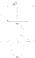
- As shown in
Figure 1 , the basic structure of the touch layer of the capacitive touch display panel includes: a dielectric material, two conductive films which are isolated by the dielectric material from each other, adriving line 11 is disposed on the lower conductive film and a detectingline 12 is disposed on the upper conductive film. In the case where there is no touch made by the touch body, the equivalent circuit of the touch layer is as shown inFigure 2 . Specifically, a capacitance C1 is formed between thedriving line 11 and thedetecting line 12, and thedriving line 11 and thedetecting line 12 respectively has an equivalent resistance R2 and an equivalent resistance R3; thedetecting line 12 is grounded via a resistance R1; thedriving line 11 and the detectingline 12 respectively has a parasitic capacitance C2 and a parasitic capacitance C3 with respect to other conductive layer(s) of the display panel; the parasitic capacitance C2 of thedriving line 11 is connected in series to the resistor R4 and then grounded; and the parasitic capacitance C3 of thedetecting line 12 is connected in series to the resistance R5 and then grounded. In this case, if an alternate current signal I0 is applied to thedriving line 11, the voltage Vs of a corresponding signal will be detected from thedetecting line 12. In the case where the touch body (such as a finger) touches the touch layer, such as thedetecting line 12, as shown inFigure 3 , the equivalent circuit of the touch layer is as shown inFigure 4 . Specifically, thefinger 12 applies a grounding capacitance C5 to the detectingline 12, and the equivalent resistance of the finger is R6. In this case, if the alternate current signal I0 is still applied to thedriving line 11, the voltage Vs of the corresponding signal detected from the detectingline 12 will be smaller, since the resistance R6, the grounding capacitance C5 and the capacitance C1 are connected in series sequentially. In summary, whether the touch layer is touched may be known according to the voltage detected from the detectingline 12. - Combining the above-mentioned IPS, FFS liquid crystal display and the capacitive touch display panel, the IPS, FFS liquid crystal display (FFS-LCD) touch display panel is formed and include(s): a color film (CF) substrate, a thin film transistor (TFT) substrate and a liquid crystal layer therebetween. The touch layer is disposed on the CF substrate. However, in the above-mentioned FFS-LCD touch display panel, the driving lines and the detecting lines are disposed all over the entire layer, and thus the driving lines and the detecting lines are completely overlapped with the upper electrode layer (the pixel electrode or the common electrode) having the comb-shaped structure respectively. The liquid crystal is filled between the driving and detecting lines and the upper electrode layer. The liquid crystal is equivalent to be the dielectric material, the driving lines and the detecting lines are equivalent to be one electrode plate, and the upper electrode layer having the slit(s) is equivalent to be the other electrode plate. Therefore, there may be parasitic capacitances existed between the driving lines and the upper electrode layer having the comb-shaped structure, and between the detecting lines and the upper electrode layer. As for the above-mentioned touch detecting method, the parasitic capacitance may cause the voltage Vs detected from the detecting line to become smaller, therefore reducing the detection sensitivity of the touch display panel. For the IPS-LCD touch display panel, the driving lines and the detecting lines disposed all over the entire layer may also lead to parasitic capacitances existed between the driving and detecting lines and the common and pixel electrodes which are separated, thus reducing the detection sensitivity of the touch display panel.
-
US patent application No. 2012169636A1 discloses a touchable sensing matrix unit, where a common electrode layer takes the form of a comb, a grid or a curved comb.US patent application No. 2011187677A1 discloses liquid-crystal display (LCD) touch screens that integrate the touch sensing elements with the display circuitry, where electrodes having a comb-shaped structure can be used to orient the liquid crystal layer during display updating, and can also be used to achieve touch sensing in combination with additional elements such as switches to change the drives for a set of signal lines based on whether the pixel is undergoing display updating or touch-sensing, or capacitances and two transistors to control when the electrodes will be used for display updating or touch sensing. - Based on this situation, the present invention provides a touch display panel to improve the above-motioned problems.
- The object of the invention is to provide a touch display panel, so as to reduce the parasitic capacitances between the driving line and the upper electrode layer having the comb-shaped structure (or the common and pixel electrodes which are separated), and between the detecting line and the upper electrode layer, thereby improving the detection sensitivity of the touch display panel.
- According to the invention, it is provided a touch display panel, which includes: a color film (CF) substrate and a thin film transistor (TFT) substrate disposed opposite to each other, and a liquid crystal layer disposed between the CF substrate and the TFT substrate, herein, a common electrode having a comb-shaped structure and/or a pixel electrode having a comb-shaped structure is disposed on a surface of the TFT substrate which is close to the liquid crystal layer, a touch layer is disposed on a surface of the CF substrate which is close to the liquid crystal layer, the touch layer includes a driving line and a detecting line which are insulated from each other, and the driving line and/or the detecting line has a comb-shaped structure which is at least partially misaligned with respect to the comb-shaped structure of the common electrode and/or the comb-shaped structure of the pixel electrode.
- Optionally, the comb-shaped structure of the driving line and/or the detecting line is complementary to the comb-shaped structure of the common electrode and/or the comb-shaped structure of the pixel electrode.
- Optionally, the driving line and the detecting line are formed in a same layer, and the driving line is perpendicular to the detecting line.
- Optionally, the detecting line is separated into separated portions by the driving line, and a first connecting portion is disposed on the separated portions, and the first connecting portion crosses the driving line to connect the separated portions of the detecting line.
- Optionally, the driving line is separated into separated portions by the detecting line, and a second connecting portion is disposed on the separated portions, and the second connecting portion crosses the detecting line to connect the separated portions of the driving line.
- Optionally, the touch layer includes a first touch layer and a second touch layer which are insulated from each other, the driving line is formed in the first touch layer, and the detecting line is formed in the second touch layer.
- Optionally, the second touch layer is closer to the liquid crystal layer than the first touch layer, and the detecting line has a comb-shaped structure which is misaligned with respect to the comb-shaped structure of the common electrode and/or the comb-shaped structure of the pixel electrode.
- Optionally, the first touch layer is closer to the liquid crystal layer than the second touch layer, and the driving line has a comb-shaped structure which is misaligned with respect to the comb-shaped structure of the common electrode and/or the comb-shaped structure of the pixel electrode.
- Optionally, the common electrode is disposed on a surface of the TFT substrate close to the liquid crystal layer, the common electrode has a comb-shaped structure, and the comb-shaped structure of the driving line and/or the detecting line being at least partially misaligned with respect to the comb-shaped structure of the common electrode.
- Optionally, the pixel electrode is disposed on a surface of the TFT substrate close to the liquid crystal layer, the pixel electrode has a comb-shaped structure, and the comb-shaped structure(s) of the driving line and/or the detecting line is being at least partially misaligned with respect to the comb-shaped structure of the pixel electrode.
- Optionally, the common electrode and the pixel electrode are disposed on the surface of the TFT substrate, said surface is close to the liquid crystal layer, the common electrode and the pixel electrode have comb-shaped structures separated with each other, and the comb-shaped structure of the driving line and/or the detecting line being at least partially misaligned with respect to both the comb-shaped structure of the common electrode and the comb-shaped structure of the pixel electrode.
- Optionally, the materials of the driving line and the detecting line are transparent.
- Optionally, the material of the common electrode or the pixel electrode is transparent.
- Optionally, the materials of the driving line and the detecting line are indium tin oxide, indium zinc oxide or the combination thereof.
- Compared with the prior art, the present invention has the following advantages.
- 1) For the IPS-LCD touch display panel, both the common electrode and the pixel electrode disposed on the TFT substrate close to the liquid crystal layer have comb-shaped structures. The arrangement for the touch layer of the CF substrate is different from the existing solution in which the driving line and the detecting line are disposed all over the entire layer. According to the present invention, the driving line and/or the detecting line has comb-shaped structure, the comb-shaped structure is at least partially misaligned with respect to at least one of the comb-shaped structure of the common electrode and the comb-shaped structure of the pixel electrode which are disposed on the TFT substrate close to the liquid layer. Therefore, it is avoided that the common electrode and/or pixel electrode of the TFT substrate being completely overlapped with the driving line and/or the detecting line of the CF substrate, thereby reducing the parasitic capacitance; and
For the FFS-LCD touch display panel, the common electrode having a comb-shaped structure or the pixel electrode having a comb-shaped structure is disposed on the TFT substrate close to the liquid crystal layer. The arrangement for the touch layer of the CF substrate is different from the existing solution in which the driving line and the detecting line are disposed all over the entire layer. According to the present invention, the driving line and/or the detecting line is also disposed in a comb-shaped structure which is at least partially misaligned with respect to one of the comb-shaped structure of the common electrode or the comb-shaped structure of the pixel electrode which is disposed on the TFT substrate close to the liquid layer. Therefore, it is avoided that the common electrode and/or pixel electrode of the TFT substrate are completely overlapped with the driving line and/or the detecting line of the CF substrate, thereby reducing the parasitic capacitance. - 2) In the optional solution, for the IPS-LCD touch display panel, the comb-shaped structure of the driving line and/or the detecting line is at least partially not only misaligned with respect to but also complementary to at least one of the comb-shaped structure of the common electrode and the comb-shaped structure of the pixel electrode which are disposed on the TFT substrate close to the liquid layer, thereby further reducing the parasitic capacitances between the common electrode and/or the pixel electrode of the TFT substrate and the driving line and/or the detecting line of the CF substrate; and
for the FFS-LCD touch display panel, the comb-shaped structure of the driving line and/or the detecting line is at least partially not only misaligned with respect to but also complementary to one of the comb-shaped structure of the common electrode or the comb-shaped structure of the pixel electrode which is disposed on the TFT substrate close to the liquid layer, thereby further reducing the parasitic capacitances between the common electrode and/or the pixel electrode of the TFT substrate and the driving line and/or the detecting line of the CF substrate. -
-
Figure 1 is a structural diagram in the case where a touch layer of a capacitive touch display panel is not touched in the prior art; -
Figure 2 is the equivalent circuit diagram ofFigure 1 ; -
Figure 3 is a structural diagram in the case where the touch layer of the capacitive touch display panel is touched in the prior art; -
Figure 4 is the equivalent circuit diagram ofFigure 3 ; -
Figure 5 is a structural diagram of a touch display panel according to the present invention; -
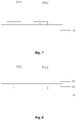
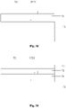
Figure 6 is a plan view of a pixel unit of the first kind of TFT substrate of an IPS-LCD touch display panel; -
Figure 7 is a sectional view taken along line I-I inFigure 6 ; -
Figure 8 is a structural sectional view of an optimized structure of the structure inFigure 7 ; -
Figure 9 is a structural diagram of a driving line according to the present invention; -
Figure 10 is a structural diagram of a detecting line according to the present invention; -
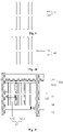
Figure 11 is a plan view of a touch panel formed by a CF substrate and the pixel unit of the TFT substrate inFigure 6 ; -
Figure 12 is a sectional view taken along line II-II inFigure 11 ; -
Figure 13 is a plan view of a pixel unit of the second kind of TFT substrate of the IPS-LCD touch display panel; -
Figure 14 is a structural diagram of a touch layer according to the present invention; -
Figure 15 is an enlarged view of the region Q inFigure 14 ; -
Figure 16 is a sectional view of the third kind of TFT substrate of the IPS-LCD touch display panel; -
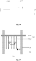
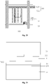
Figure 17 is a plan view of a pixel unit of a TFT substrate of an FFS-LCD touch display panel; -
Figure 18 is a sectional view taken along line III-III inFigure 17 ; -
Figure 19 is a structural sectional view of an optimized structure of the structure inFigure 18 ; -
Figure 20 is a plan view of a touch panel form by a CF substrate and the pixel unit of the TFT substrate inFigure 17 ; and -
Figure 21 is a sectional view taken along line IV-IV inFigure 20 . - To make the above object, features and advantages of the invention more obvious and easy to be understood, in the following, particular embodiments of the invention will be illustrated in detail in conjunction with the drawings. The invention mainly focused on the explanation of the principle and the accompanying drawings may not be drawn to scale.
- For convenience in understanding the technical solution of the invention, all of the numerical references appeared in the invention are listed as follows:
driving line 11detecting line 12CF substrate 2TFT substrate 3liquid crystal layer 4glass substrate 31electrode layer 32 gate line 33data line 34pixel electrode 321bar portion of pixel electrode 3211comb-shaped portion of pixel electrode 3212common electrode 322bar portion of common electrode 3221comb-shaped portion of common electrode 3222protective film 35alignment layer 36driving line 22detecting line 24bar portion of driving line 221comb-shaped portion of driving line 222bar portion of detecting line 241comb-shaped portion of detecting line 242passivation layer 37insulating layer 38dielectric layer 23glass substrate 21 - In the first embodiment, an IPS-LCD touch display panel which operates in the IPS liquid display mode is taken as an example to explain the technical solution of the invention.
- Referring to
Figure 5 , the IPS-LCD touch display panel includes: a color film (CF)substrate 2 and a thin film transistor (TFT)substrate 3 disposed opposite to each other, and aliquid crystal layer 4 disposed between the CF substrate and the TFT substrate. - The
TFT substrate 3 is firstly described. Referring toFigure 6 which is a plan view of a pixel unit andFigure 7 which is a sectional view taken along line I-I inFigure 6 , theTFT substrate 3 includes aglass substrate 31 and a circuit board formed on theglass substrate 31. The surface of the circuit board close to theliquid crystal layer 4 is an electrode layer 32 including acommon electrode 322 and apixel electrode 321 which are used for providing a voltage to rotate the liquid crystal. - The circuit board includes a
data line 34 and agate line 33 intersecting with each other, a TFT transistor formed at the intersection of thedata line 34 and thegate line 33, and apixel electrode 321 formed in a region defined by thedata line 34 and thegate line 33. Furthermore, the circuit board further includes: a common electrode line (not shown) disposed in the same layer as with thegate line 33 and substantially in parallel with thegate line 33; and acommon electrode 322 electrically connected to the common electrode line. The gate electrode of the TFT transistor is a portion of thegate line 33, the source electrode of the TFT transistor is a portion of thedata line 34, and the drain electrode of the TFT transistor is connected to thepixel electrode 321 via a via hole (not shown). Thepixel electrode 321 includes abar portion 3211 and a comb-shapedportion 3212 connected perpendicularly to thebar portion 3211. A portion of thecommon electrode 322 is also formed in the same layer as with thepixel electrode 321. Thecommon electrode 322 has abar portion 3221 being substantially parallel with the common electrode line and a comb-shapedportion 3222 substantially in perpendicular to the common electrode line. The comb-shapedportion 3222 and the comb-shapedportion 3212 of thepixel electrode 321 are disposed in an alternate arrangement, for a voltage to rotate the liquid crystal molecules. - In the above-mentioned structure, the
bar portion 3221 and the comb-shapedportion 3222 form the comb-shaped structure of thecommon electrode 322, and thebar portion 3211 and the comb-shapedportion 3212 form the comb-shaped structure of thepixel electrode 321. The purpose of disposing the comb-shaped portions for thecommon electrode 322 and thepixel electrode 321 respectively is to dispose discontinuous gaps (slits) for the integral structure on one's own, so as to dispose an opening portion for making the electrical field pass through. Therefore, for other embodiments, it is not limited to the comb-shaped structure, as long as the discontinuous gaps can be formed respectively in thecommon electrode 322 and thepixel electrode 321. - Furthermore, the comb-shaped structure of the
common electrode 322 and the comb-shaped structure of thepixel electrode 321 are formed on the surface of theTFT substrate 3 close to theliquid crystal layer 4. In order to improve the service life of both the comb-shaped structure of thecommon electrode 322 and the comb-shaped structure of thepixel electrode 321, as shown inFigure 8 , aprotective film 35 may be disposed on the comb-shapedportion 3222 of thecommon electrode 322 and the comb-shapedportion 3212 of thepixel electrode 321, and the material of theprotective film 35 may be silicon nitride. More preferably, a liquid crystal alignment layer36 may further be disposed on theprotective film 35, and the material of the liquidcrystal alignment layer 36 may be polyimide. - It should be noted that the
glass substrate 31 may also be made of a transparent material such as quartz or flexible plastic as required. - The
CF substrate 2 is described as follows. Referring toFigure 5 , theCF substrate 2 includes aglass substrate 21, a light filter layer (not shown) disposed on the surface of theglass substrate 21, a light-blocking layer (not shown) and a touch layer close to theliquid crystal layer 4. The touch layer includes a first touch layer and a second touch layer. A drivingline 22 is formed in the first touch layer, and a detectingline 24 is formed in the second touch layer. Adielectric layer 23 is disposed between the two touch layers. - Preferably, in the two touch layers, the driving
line 22 and the detectingline 24 are disposed perpendicularly to each other, so that a touch control signal is detected when a touching body makes a touch at the intersection of the drivingline 22 and the detectingline 24. - In the first embodiment, the second touch layer disposed with the detecting
line 24 is closer to theliquid crystal layer 4. However, in other embodiments, the first touch layer disposed with the drivingline 22 may be closer to theliquid crystal layer 4. - It should be noted that one unit formed by one driving
line 22 and one detectingline 24 may correspond to one pixel unit of theTFT substrate 3 or correspond to multiple pixel units. - In the prior art, each of the driving
line 22 and the detectingline 24 is an integral conductive layer. Unlike the prior art, in the first embodiment, the drivingline 22 or the detectingline 24 is also disposed in a comb-shaped structure. Specifically, referring toFIG 9 , the comb-shaped structure of the drivingline 22 includes abar portion 221 and a comb-shapedportion 222 connected in perpendicular to thebar portion 221. Referring toFigure 10 , the comb-shaped structure of the detectingline 24 includes abar portion 241 and a comb-shapedportion 242 connected in perpendicular to thebar portion 241. - Furthermore, as for the case where the comb-shaped
portion 3222 of thecommon electrode 322 and the comb-shapedportion 3212 of thepixel electrode 321 are on a same layer and disposed alternately, and the detectingline 24 is closer to theliquid crystal layer 4, the detectingline 24 is specifically disposed as follows. 1) The comb-shapedportion 242 of the detectingline 24 is misaligned with respect to the comb-shapedportion 3212 of thepixel electrode 321; or 2) the comb-shapedportion 242 of the detectingline 24 is misaligned with respect to the comb-shapedportion 3222 of thecommon electrode 322; or 3) the comb-shapedportion 242 of the detectingline 24 is misaligned with respect to both the comb-shapedportion 3212 of thepixel electrode 321 and the comb-shapedportion 3222 of thecommon electrode 322. Thus it is avoided that thecommon electrode 322 and thepixel electrode 321 of theTFT substrate 3 are completely overlapped with the detectingline 22 of theCF substrate 2, thereby reducing the parasitic capacitance. - As for the case where the comb-shaped
portion 3222 of thecommon electrode 322 and the comb-shapedportion 3212 of thepixel electrode 321 are on a same layer and disposed alternately, and the drivingline 22 is closer to theliquid crystal layer 4, the drivingline 22 is specifically disposed as follows. 1) The comb-shapedportion 222 of the drivingline 22 is misaligned with respect to the comb-shapedportion 321 of thepixel electrode 321; or 2) the comb-shapedportion 222 of the drivingline 22 is misaligned with respect to the comb-shapedportion 3222 of thecommon electrode 322; or 3) the comb-shapedportion 222 of the drivingline 22 is misaligned with respect to both the comb-shapedportion 3212 of thepixel electrode 321 and the comb-shapedportion 3222 of thecommon electrode 322. Thus it is avoided that thecommon electrode 322 and thepixel electrode 321 of theTFT substrate 3 are completely overlapped with the drivingline 22 of theCF substrate 2, thereby reducing the parasitic capacitance. For the case of 3), in order to show clearly the technical solution of the first embodiment of the invention,Figure 11 shows a plan view of a display panel corresponding to one pixel unit when theCF substrate 2 and theTFT substrate 3 are in position andFigure 12 shows a sectional view taken along line II-II inFigure 11 . As can be seen inFigure 11 andFigure 12 , the drivingline 22 of theCF substrate 2 is misaligned respectively with respect to the comb-shapedportion 3212 of the pixel electrode and the comb-shapedportion 3222 of the common electrode of theTFT substrate 3 which are respectively disposed in two layers. - In short, the comb-shaped structure of the driving
line 22 or the detectingline 24 is at least partially misaligned with respect to the comb-shaped structure of thecommon electrode 322 and/or the comb-shaped structure of thepixel electrode 321 in theTFT substrate 3 close to theliquid crystal layer 4. Thus it is avoided that the common electrode 433322 and thepixel electrode 321 of theTFT substrate 3 are completely overlapped with the drivingline 22 and/or the detectingline 24 of theCF substrate 2, thereby reducing the parasitic capacitance. - As shown in
Figure 6 , thebar portion 3221 of thecommon electrode 322 is disposed at one end of the comb-shapedportion 3222. It can be understood that thebar portion 3221 is not limited to be disposed at one end of the comb-shapedportion 3222 and may also be disposed in the middle of the comb-shapedportion 3222 as shown inFigure 13 , in order to form the incontinuous gaps. - Furthermore, there are multiple comb-shaped
portions 3222 connected to thebar portion 3221 of onecommon electrode 322 and there are multiple comb-shapedportions 3212 connected to thebar portion 3211 of onepixel electrode 321. However, it should be noted that, for thecommon electrode 322, the multiple connected comb-shapedportions 3222 are not limited to be connected to onebar portion 3221 and may also be connected tomultiple bars portions 3221. Similarly, for thepixel electrode 321, the multiple connected comb-shapedportions 3212 are not limited to be connected to onebar portion 3211 and may also be connected tomultiple bar portions 3211. Correspondingly, for the drivingline 22, multiple connected comb-shapedportions 222 are not limited to be connected to onebar portion 221 and may also be connected tomultiple bar portions 221. Similarly, for the detectingline 24, the multiple connected comb-shapedportions 242 are not limited to be connected to onebar portion 241 and may also be connected tomultiple bar portions 241. - Similarly, the
bar portion 221 and the comb-shapedportion 222 form the comb-shaped structure of the drivingline 22. Thebar portion 241 and the comb-shapedportion 242 form the comb-shaped structure of the detectingline 24. The respective comb-shaped structures are disposed in order to dispose the discontinuous gaps (slits) for the respective integral structures, so as to dispose opening portions for making the electrical field pass through. Therefore, other embodiments are not limited to the comb-shaped structure, as long as the discontinuous gaps can be formed respectively for the drivingline 22 and the detectingline 24. - In summary, for the IPS-LCD touch display panel according to the first embodiment, on the
TFT substrate 3 close to theliquid crystal layer 4, thecommon electrode 322 and thepixel electrode 321 are on a same layer and disposed alternately. Sine thecommon electrode 322 and thepixel electrode 321 are disposed alternately, each of thecommon electrode 322 and thepixel electrode 321 has a comb-shaped structure. As for the above-mentioned, thecommon electrode 322 and thepixel electrode 321 are disposed in the same layer, and the touch layer is disposed on theCF substrate 2, the driving line and the detecting line are disposed all over the entire layer in the prior art. However, according to the present invention, it is different that the drivingline 22 or the detectingline 24 is disposed in a comb-shaped structure as well, and the comb-shaped structure is at least partially misaligned with respect to at least one of the comb-shaped structure of thecommon electrode 322 and the comb-shaped structure of thepixel electrode 321 in the same layer. Thus it is avoided that thecommon electrode 322 and/or thepixel electrode 321 of theTFT substrate 3 are completely overlapped with the drivingline 22 or the detectingline 24 of theCF substrate 2, thereby reducing the parasitic capacitance. - The above-mentioned misaligning includes partially misaligning and completely misaligning. In order to increase the quantity of electrodes disposed in a plane and to improve utilization rate, the comb-shaped structure of the driving
line 22 or the detectingline 24 is at least partially complementary to the comb-shaped structure of thecommon electrode 322 and/or the comb-shaped structure of thepixel electrode 321 in the same layer. - In the first embodiment, in order to improve the light transmittance, the materials of the driving
line 22 and the detectingline 24 are transparent, such as indium tin oxide, indium zinc oxide or the combination thereof. The materials of thecommon electrode 322, thegate line 33 and thedata line 34 may be metal such as copper and aluminum. The materials of thecommon electrode 322, thegate line 33 and thedata line 34 may also be a transparent conductive material, so as to increase the light transmittance. The material of the pixel electrode 312 is generally a transparent conductive material. The transparent conductive material may also be, for example, indium tin oxide, indium zinc oxide or the combination thereof. - Besides the driving
line 22 or the detectingline 24 disposed on the surface of theCF substrate 2, a liquid crystal alignment layer made of polyimide may also be disposed on the drivingline 22 or the detectingline 24. - The structure of the touch display panel according to the second embodiment is substantially the same as the structure of the touch display panel according to the first embodiment, except that, for the
CF substrate 2, the drivingline 22 and detectingline 24 are disposed in one touch layer, rather than that the drivingline 22 and the detectingline 24 are respectively disposed in two touch layers, as shown inFigure 14 . The drivingline 22 and the detectingline 24 are isolated with each other via adielectric layer 23. Furthermore, in the second embodiment, the drivingline 22 separates the detectingline 24 into separated portions. On the separated portions, a first connectingportion 25 is disposed to connect the separated detectingline 24 across the drivingline 22. In other embodiment, the detectingline 24 may also separate thedriving line 22 into separated portions. A second connecting portion is disposed on the separated portions, the first connecting portion crosses the detectingline 24 to connect the separated drivingline 22. -
Figure 15 shows an enlarged view of the region Q inFigure 14 . The comb-shaped structure of the drivingline 22 includes abar portion 221 and a comb-shapedportion 222 connected in perpendicular to thebar portion 221. The comb-shaped structure of the detectingline 24 includes abar portion 241 and a comb-shapedportion 242 connected in perpendicular to thebar portion 241. - Furthermore, as for the case where the comb-shaped
portion 3222 of thecommon electrode 322 and the comb-shapedportion 3212 of thepixel electrode 321 are on a same layer and disposed alternately, and the drivingline 22 and the detectingline 24 are disposed in one touch layer, the touch layer is specifically disposed as follows. 1) One of the comb-shaped portion 222 of the driving line 22 and the comb-shaped portion 242 of the detecting line 24 is misaligned with respect to the comb-shaped portion 3212 of the pixel electrode 321, or, both of the comb-shaped portion 222 of the driving line 22 and the comb-shaped portion 242 of the detecting line 24 are misaligned with respect to the comb-shaped portion 3212 of the pixel electrode 321; or 2) one of the comb-shaped portion 222 of the driving line 22 and the comb-shaped portion 242 of the detecting line 24 is misaligned with respect to the comb-shaped portion 3222 of the common electrode 322, or, both of the comb-shaped portion 222 of the driving line 22 and the comb-shaped portion 242 of the detecting line 24 are misaligned with respect to the comb-shaped portion 3222 of the common electrode 322; or 3) one of the comb-shaped portion 222 of the driving line 22 and the comb-shaped portion 242 of the detecting line 24 is misaligned with respect to both the comb-shaped portion 3212 of the pixel electrode 321 and the comb-shaped portion 3222 of the common electrode 322, or, both of the comb-shaped portion 222 of the driving line 22 and the comb-shaped portion 242 of the detecting line 24 are misaligned with respect to both the comb-shaped portion 3212 of the pixel electrode 321 and the comb-shaped portion 3222 of the common electrode 322. Thus it is avoided that thecommon electrode 322 and/or thepixel electrode 321 of theTFT substrate 3 are/is completely overlapped with the detectingline 24 and/or the drivingline 22 of theCF substrate 2, thereby reducing the parasitic capacitance. - In short, the comb-shaped structure of the driving
line 22 and/or the detectingline 24 is at least partially misaligned with respect to at least one of the comb-shaped structure of thecommon electrode 322 and the comb-shaped structure of thepixel electrode 321 in theTFT substrate 3 close to theliquid crystal layer 4. - The above-mentioned misaligning includes partially misaligning and completely misaligning. In order to increase the quantity of electrodes disposed in a plane and to improve utilization rate, the comb-shaped structure of the driving
line 22 and/or the detectingline 24 is at least partially complementary to the comb-shaped structure of thecommon electrode 322 and/or the comb-shaped structure of thepixel electrode 321 in theTFT substrate 3 close to theliquid crystal layer 4. - The structure of the touch display panel according to the third embodiment is substantially the same as the structure of the touch display panel according to the first embodiment, the different is that for the
TFT substrate 3, thecommon electrode 322 and thegate line 33 are firstly formed on theglass substrate 31 and then the TFT structure and thepixel electrode 321 are formed. Therefore, the comb-shapedportion 3222 of thecommon electrode 322 and the comb-shapedportion 3212 of thepixel electrode 321 may not be formed in the same layer, as shown inFigure 16 , one or more insulating layer such as apassivation layer 37 is disposed between the comb-shapedportion 3222 of thecommon electrode 322 and the comb-shapedportion 3212 of thepixel electrode 321. - As for the case where the comb-shaped
portion 3212 of thepixel electrode 321 is closer to theliquid crystal layer 4 than the comb-shapedportion 3222 of thecommon electrode 322 and the detectingline 24 is closer to theliquid crystal layer 4, the touch layer is specifically disposed as follows. The comb-shapedportion 242 of the detectingline 24 is misaligned with respect to the comb-shapedportion 3212 of thepixel electrode 321. Thus it is avoided that thepixel electrode 321 of theTFT substrate 3 is completely overlapped with the detectingline 24 of theCF substrate 2, thereby reducing the parasitic capacitance. - As for the case where the comb-shaped
portion 3212 of thepixel electrode 321 is closer to theliquid crystal layer 4 than the comb-shapedportion 3222 of thecommon electrode 322 and the drivingline 22 is closer to theliquid crystal layer 4, the touch layer is specifically disposed as follows. The comb-shapedportion 222 of the drivingline 22 is misaligned with respect to the comb-shapedportion 3212 of thepixel electrode 321. Thus it is avoided that thepixel electrode 321 of theTFT substrate 3 is completely overlapped with the drivingline 22 of theCF substrate 2, thereby reducing the parasitic capacitance. - As for the case where the comb-shaped
portion 3212 of thepixel electrode 321 is closer to theliquid crystal layer 4 than the comb-shapedportion 3222 of thecommon electrode 322, and the drivingline 22 and the detectingline 24 are disposed in the same touch layer, the touch layer is specifically disposed as follows. Both of the comb-shapedportion 222 of the drivingline 22 and the comb-shapedportion 242 of the detectingline 24 are misaligned with respect to the comb-shapedportion 3212 of thepixel electrode 321; or one of the comb-shapedportion 222 of the drivingline 22 and the comb-shapedportion 242 of the detectingline 24 is misaligned with respect to the comb-shapedportion 3212 of thepixel electrode 321. Thus it is avoided that thepixel electrode 321 of theTFT substrate 3 is completely overlapped with the detectingline 24 and/or the drivingline 22 of theCF substrate 2, thereby reducing the parasitic capacitance. - In short, the comb-shaped structure of the driving
line 22 and/or the detectingline 24 is at least partially misaligned with respect to the comb-shaped structure of thepixel electrode 321 in theTFT substrate 3 close to theliquid crystal layer 4. Thus it is avoided that thepixel electrode 321 of theTFT substrate 3 is completely overlapped with the drivingline 22 and/or the detectingline 24 of theCF substrate 2, thereby reducing the parasitic capacitance. - As for the case where the comb-shaped
portion 3222 of thecommon electrode 322 is closer to theliquid crystal layer 4 than the comb-shapedportion 3212 of thepixel electrode 321 and the detectingline 24 is closer to theliquid crystal layer 4, the touch layer is specifically disposed as follows: The comb-shapedportion 242 of the detectingline 24 is misaligned with respect to the comb-shapedportion 3222 of thecommon electrode 322. Thus it is avoided that thecommon electrode 322 of theTFT substrate 3 is completely overlapped with the detectingline 24 of theCF substrate 2, thereby reducing the parasitic capacitance. - As for the case where the comb-shaped
portion 3222 of thecommon electrode 322 is closer to theliquid crystal layer 4 than the comb-shapedportion 3212 of thepixel electrode 321 and the drivingline 22 is closer to theliquid crystal layer 4, the touch layer is specifically disposed as follows: The comb-shapedportion 222 of the drivingline 22 is misaligned with respect to the comb-shapedportion 3222 of thecommon electrode 322. Thus it is avoided that thecommon electrode 322 of theTFT substrate 3 is completely overlapped with the drivingline 22 of theCF substrate 2, thereby reducing the parasitic capacitance. - As for the case where the comb-shaped
portion 3222 of thecommon electrode 322 is closer to theliquid crystal layer 4 than the comb-shapedportion 3212 of thepixel electrode 321 and the drivingline 22 and the detectingline 24 are disposed in the same touch layer, the touch layer is specifically disposed as follows. Both of the comb-shapedportion 222 of the drivingline 22 and the comb-shapedportion 242 of the detectingline 24 are misaligned with respect to the comb-shapedportion 3222 of thecommon electrode 322; or one of the comb-shapedportion 222 of the drivingline 22 and the comb-shapedportion 242 of the detectingline 24 is misaligned with respect to the comb-shapedportion 3222 of thecommon electrode 322. Thus it is avoided that thecommon electrode 322 of theTFT substrate 3 is completely overlapped with the detectingline 24 and/or the drivingline 22 of theCF substrate 2, thereby reducing the parasitic capacitance. - In short, the comb-shaped structure of the driving
line 22 and/or the comb-shaped structure of the detectingline 24 are/is at least partially misaligned with respect to the comb-shaped structure of thecommon electrode 322 on theTFT substrate 3 close to theliquid crystal layer 4. Thus it is avoided that thecommon electrode 322 of theTFT substrate 3 is completely overlapped with the drivingline 22 and/or the detectingline 24 of theCF substrate 2, thereby reducing the parasitic capacitance. - In summary, the comb-shaped structure of the driving
line 22 and/or the detectingline 24 are/is at least partially misaligned with respect to the comb-shaped structure of thecommon electrode 322 or the comb-shaped structure of the pixel electrode 312 on theTFT substrate 3 close to theliquid crystal layer 4. Thus it is avoided that thecommon electrode 322 or the pixel electrode 312 of theTFT substrate 3 is completely overlapped with the drivingline 22 and/or the detectingline 24 of theCF substrate 2, thereby reducing the parasitic capacitance. - The above-mentioned misaligning includes partially misaligning and completely misaligning. In order to increase the quantity of electrodes disposed in a plane and to improve utilization rate, the comb-shaped structure of the driving
line 22 and/or the detectingline 24 is at least partially complementary to the comb-shaped structure of thecommon electrode 322 or the comb-shaped structure of thepixel electrode 321 on theTFT substrate 3 close to theliquid crystal layer 4. - According to the description of the IPS mode and the FFS mode for implementing the liquid crystal display in the background. Compared with the IPS mode, the FFS mode has higher light transmittance. This is because, in the FFS mode, the common electrode and the pixel electrode do not have to be disposed alternately, leading to a reduced space therebetween. Therefore, the upper portion of the common electrode or the pixel electrode in the upper electrode layer can also generate a lateral electric field, and the liquid crystal molecules on the corresponding electrode can also be rotated. It is no longer limited to the case in the IPS mode where the lateral electric field only exist between the common electrode and the pixel electrode, each electrode almost has no electric field, and the liquid crystal molecules on each electrode can not be rotated.
- In the fourth embodiment, the FFS-LCD touch display panel which operates in the FFS liquid display mode is taken as an example to explain the technical solution of the present invention.
- Referring to
Figure 5 , the FFS-LCD touch display panel includes: a color film (CF)substrate 2 and a thin film transistor (TFT)substrate 3 disposed opposite to each other, and aliquid crystal layer 4 disposed between the CF substrate and the TFT substrate. The most difference between the FFS-LCD touch display panel and the IPS-LCD touch display panel lies in theTFT substrate 3. - The
TFT substrate 3 of the FFS-LCD touch display panel is described as follows. Referring toFigure 17 which is plan view of a pixel unit andFigure 18 which a sectional view taken along line III-III inFigure 17 , theTFT substrate 3 includes aglass substrate 31 and a circuit board formed on theglass substrate 31. The circuit board includes adata line 34 and agate line 33 intersecting with each other, a TFT transistor formed at the intersection of thedata line 34 and thegate line 33, and a common electrode (line) 322 and apixel electrode 321, the common electrode (line) 322 is substantially parallel with thegate line 33. The gate electrode of the TFT transistor is a portion of thegate line 33, the source electrode of the TFT transistor is a portion of thedata line 34, and the drain electrode of the TFT transistor is connected to thepixel electrode 321 via a via hole (not shown). Thepixel electrode 321 is an integral conductive layer. On thepixel electrode 321, an insulatinglayer 38 and thecommon electrode 322 are formed from bottom to top. Thecommon electrode 322 has abar portion 3221 substantially disposed in parallel with the common electrode line and a comb-shapedportion 3222 disposed substantially in perpendicular to the common electrode line. The comb-shapedportion 3222 and thepixel electrode 321 are used for providing a voltage to rotate the liquid crystal molecules. - In the above-mentioned structure, the
bar portion 3221 and the comb-shapedportion 3222 form the comb-shaped structure of thecommon electrode 322, in order to dispose incontinuous gaps (slits) for the integral structure, so as to dispose an opening portion for making the electrical field pass through. Therefore, other embodiments are not limited to the comb-shaped structure, as long as the discontinuous gaps can be formed for thecommon electrode 322. - Furthermore, the comb-shaped structure of the
common electrode 322 is disposed on the surface of theTFT substrate 3, the surface is close to theliquid crystal layer 4. In order to improve the service life of the comb-shaped structure of thecommon electrode 322, as shown inFigure 19 , aprotective film 35 may be disposed on the comb-shapedportion 3222 of thecommon electrode 322, and the material of theprotective film 35 may be silicon nitride. More preferably, a liquidcrystal alignment layer 36 may further be dispose on theprotective film 35, and the material of the liquidcrystal alignment layer 36 may be polyimide. - It should be noted that the
glass substrate 31 may also be made of a transparent material such as quartz or flexible plastic as required. - The
CF substrate 2 is described next. Similar to the first embodiment and the second embodiment, the touch layer may include a first touch layer and a second touch layer. The drivingline 22 is formed in the first touch layer, and the detectingline 24 is formed in the second touch layer. Adielectric layer 23 is disposed between the two touch layers. The drivingline 22 and the detectingline 24 may also be disposed in one touch layer. - In the following, the solution in which the
driving line 22 and the detectingline 24 are respectively formed in two touch layers is firstly described. - Preferably, in the two touch layer, the driving
line 22 and the detectingline 24 are disposed perpendicularly to each other, so that a touch control signal is detected when a touching body makes a touch at the intersection of the drivingline 22 and the detectingline 24. - In the fourth embodiment, the driving
line 22 and the detectingline 24 respectively formed in two touch layers may be disposed in the following two ways. 1) The second touch layer disposed with the detectingline 24 is closer to theliquid crystal layer 4 and 2) the first touch layer disposed with the drivingline 22 may be closer to theliquid crystal layer 4. - It should be noted that one unit defined by one driving
line 22 and one detectingline 24 may correspond to one pixel unit of theTFT substrate 3 or correspond to multiple pixel units. - In the prior art, each of the driving
line 22 and the detectingline 24 is an integral conductive layer. Unlike the prior art, in the fourth embodiment, the drivingline 22 or the detectingline 24 is also disposed in a comb-shaped structure. Specifically, referring again toFIG 9 , the comb-shaped structure of the drivingline 22 includes abar portion 221 and a comb-shapedportion 222 connected in perpendicular to thebar portion 221. Referring toFigure 10 , the comb-shaped structure of the detectingline 24 includes abar portion 241 and a comb-shapedportion 242 connected in perpendicular to thebar portion 241. - Furthermore, as for the case where the
common electrode 322 is disposed with the comb-shapedportion 3222, thepixel electrode 321 is in an integral structure and the detectingline 24 is closer to theliquid crystal layer 4, the touch layer is specifically disposed as follows. The comb-shapedportion 242 of the detectingline 24 is misaligned with respect to the comb-shapedportion 3222 of thecommon electrode 322. Thus it is avoided that thecommon electrode 322 of theTFT substrate 3 is completely overlapped with the detectingline 22 of theCF substrate 2, thereby reducing the parasitic capacitance. - As for the case where the
common electrode 322 is disposed with the comb-shapedportion 3222, thepixel electrode 321 is in an integral structure and the drivingline 22 is closer to theliquid crystal layer 4, the touch layer is specifically disposed as follows. The comb-shapedportion 222 of the drivingline 22 is misaligned with respect to the comb-shapedportion 3222 of thecommon electrode 322. Thus it is avoided that thecommon electrode 322 of theTFT substrate 3 is completely overlapped with the drivingline 22 of theCF substrate 2, thereby reducing the parasitic capacitance. For the above-mentioned case, in order to show the technical solution of the fourth embodiment of the invention clearly,Figure 20 shows a plan view of a display panel corresponding to one pixel unit when theCF substrate 2 and theTFT substrate 3 are in position andFigure 21 shows a sectional view taken along line IV-IV inFigure 20 . As can be seen inFigure 20 and Figure 21 , the drivingline 22 of theCF substrate 2 is misaligned respectively with respect to the comb-shapedportion 3212 of the pixel electrode and the comb-shapedportion 3222 of the common electrode of theTFT substrate 3, the pixel electrode and the common electrode are respectively disposed in two layers. - In short, the comb-shaped structure of the driving
line 22 or the detectingline 24 is at least partially misaligned with respect to the comb-shaped structure of thecommon electrode 322 on theTFT substrate 3 close to theliquid crystal layer 4. Thus it is avoided that thecommon electrode 322 of theTFT substrate 3 is completely overlapped with the drivingline 22 or the detectingline 24 of theCF substrate 2, thereby reducing the parasitic capacitance. - It can be understood that there are multiple comb-shaped
portions 3222 connected to thebar portion 3221 of onecommon electrode 322. However, it should be noted that, for thecommon electrode 322, the multiple connected comb-shapedportions 3222 are not limited to be connected to onebar portion 3221 and may also be connected tomultiple bars portions 3221. Correspondingly, for the drivingline 22, multiple connected comb-shapedportions 222 are not limited to be connected to onebar portion 221 and may also be connected tomultiple bar portions 221. Similarly, for the detectingline 24, the multiple connected comb-shapedportions 242 are not limited to be connected to onebar portion 241 and may also be connected tomultiple bar portions 241. - Similarly, the
bar portion 221 and the comb-shapedportion 222 form the comb-shaped structure of the drivingline 22. Thebar portion 241 and the comb-shapedportion 242 form the comb-shaped structure of the detectingline 24. The respective comb-shaped structures are disposed in order to dispose the incontinuous gaps (slits) for the respective integral structures, so as to dispose opening portions for making the electrical field pass through. Therefore, for other embodiments, both the detectingline 24 and the drivingline 22 are not limited to be disposed in the comb-shaped structure, as long as the discontinuous gaps can be formed respectively for the drivingline 22 and the detectingline 24. - In the following, the solution in which the
driving line 22 and the detectingline 24 are formed in one touch layer is described. - Referring again to
Figure 14 , the drivingline 22 and the detectingline 24 are separated by adielectric layer 23. The drivingline 22 and the detectingline 24 are separated with each other in the following two ways. 1) The drivingline 22 separates the detectingline 24 into separated portions, a first connectingportion 25 is disposed on the separated portions, the first connectingportion 25 crosses the drivingline 22 to connect the separated detectingline 24; 2) the detectingline 24 may also separate thedriving line 22 into separated portions, a second connecting portion is disposed on the separated portions, the second connectingportion 25 crosses the detectingline 24 to connect the separated drivingline 22. - In the prior art, each of the driving
line 22 and the detectingline 24 is an integral conductive layer. Unlike the prior art, in the fourth embodiment, the drivingline 22 or the detectingline 24 is also disposed in a comb-shaped structure. Specifically, referring toFIG 9 , the comb-shaped structure of the drivingline 22 includes abar portion 221 and a comb-shapedportion 222 connected in perpendicular to thebar portion 221. Referring toFigure 10 , the comb-shaped structure of the detectingline 24 includes abar portion 241 and a comb-shapedportion 242 connected in perpendicular to thebar portion 241. - Furthermore, as for the case where the
common electrode 322 is disposed with the comb-shapedportion 3222, thepixel electrode 321 is disposed in an integral structure and the drivingline 22 and the detectingline 24 are disposed in one touch layer, the touch layer is specifically disposed as follows. One of the comb-shapedportion 222 of the drivingline 22 and the comb-shapedportion 242 of the detectingline 24 is misaligned with respect to the comb-shapedportion 3222 of thecommon electrode 322; or both of the comb-shapedportion 222 of the drivingline 22 and the comb-shapedportion 242 of the detectingline 24 are misaligned with respect to the comb-shapedportion 3222 of thecommon electrode 322. Thus it is avoided that thecommon electrode 322 of theTFT substrate 3 is completely overlapped with the detectingline 24 and/or the drivingline 22 of theCF substrate 2, thereby reducing the parasitic capacitance. - In short, the comb-shaped structure of the driving
line 22 or/and the detectingline 24 is at least partially misaligned with respect to the comb-shaped structure of thecommon electrode 322 on theTFT substrate 3 close to theliquid crystal layer 4. Thus it is avoided that thecommon electrode 322 of theTFT substrate 3 is completely overlapped with the drivingline 22 and/or the detectingline 24 of theCF substrate 2, thereby reducing the parasitic capacitance. - The above-mentioned misaligning includes partially misaligning and completely misaligning. In order to increase the quantity of electrodes disposed in a plane and to improve utilization rate, the comb-shaped structure of the driving
line 22 and/or the detectingline 24 is at least partially complementary to the comb-shaped structure of thecommon electrode 322 on theTFT substrate 3 close to theliquid crystal layer 4. - Besides the driving
line 22 or the detectingline 24 disposed on the surface of theCF substrate 2, a liquid crystal alignment layer made of polyimide may also be disposed on the drivingline 22 or the detectingline 24. - The structure of FFS-LCD touch display panel of the fifth embodiment is substantially the same as the structure of the touch display panel of the fourth embodiment, the difference is that for the
TFT substrate 3, thecommon electrode 322 and the gate electrode are disposed in the same layer and are substantially parallel with each other, and thecommon electrode 322 is an integral conductive layer. On thecommon electrode 322, an insulatinglayer 38 and thepixel electrode 321 are formed from bottom to top. Thepixel electrode 321 is connected to the drain electrode via a hole. Thepixel electrode 321 includes abar portion 3211 and a comb-shapedportion 3212 connected in perpendicular to thebar portion 3211. The comb-shapedportion 3212 and thecommon electrode 322 are used for providing a voltage to rotate the liquid crystal molecules. - In the above-mentioned structure, in order to dispose incontinuous gaps (slits) for the integral structure(s), the
bar portion 3211 and the comb-shapedportion 3212 form the comb-shaped structure of thepixel electrode 321, so as to dispose an opening portion for making the electrical field pass through. Therefore, for other embodiments, thepixel electrode 321 is not limited to the comb-shaped structure, as long as the discontinuous gaps can be formed for thepixel electrode 321. - Furthermore, the comb-shaped structure of the
pixel electrode 321 is formed on the surface of the TFT substrate, the surface is close to theliquid crystal layer 4. In order to improve the service life of the comb-shaped structure of thepixel electrode 321, a protective film may be disposed over the comb-shapedportion 3212 of thepixel electrode 321, and the material of the protective film may be silicon nitride. More preferably, a liquid crystal alignment layer made of polyimide may further be disposed on the protective film. - The
CF substrate 2 is described as follow. Similar to the fourth embodiment, the touch layer may be disposed in the following two ways. 1) The touch layer may include a first touch layer and a second touch layer; a drivingline 22 is formed in the first touch layer; a detectingline 24 is formed in the second touch layer; and adielectric layer 23 is disposed between the two touch layers. 2) The drivingline 22 and the detectingline 24 are formed in one touch layer. - In the following, the solution in which the
driving line 22 and the detectingline 24 are respectively formed in two touch layers is firstly described. - Preferably, in the two touch layer, the driving
line 22 and the detectingline 24 are disposed perpendicularly to each other, so that a touch control signal may be detected when a touching body makes a touch at the intersection of the drivingline 22 and the detectingline 24. - In the fifth embodiment, the driving
line 22 and the detectingline 24 respectively formed in two touch layers may be disposed in the following two ways. 1) The second touch layer disposed with the detectingline 24 is closer to theliquid crystal layer 4 and 2) the first touch layer disposed with the drivingline 22 may be closer to theliquid crystal layer 4. - It should be noted that one unit defined by one driving
line 22 and one detectingline 24 may correspond to one pixel unit of theTFT substrate 3 or correspond to multiple pixel units. - In the prior art, each of the driving
line 22 and the detectingline 24 is an integral conductive layer. Unlike the prior art, in the fifth embodiment, the drivingline 22 or the detectingline 24 is also disposed in a comb-shaped structure. Specifically, referring toFIG 9 , the comb-shaped structure of the drivingline 22 includes abar portion 221 and a comb-shapedportion 222 connected in perpendicular to thebar portion 221. Referring toFigure 10 , the comb-shaped structure of the detectingline 24 includes abar portion 241 and a comb-shapedportion 242 connected in perpendicular to thebar portion 241. - Furthermore, as for the case where the
pixel electrode 321 is disposed with the comb-shapedportion 3212, thecommon electrode 322 is in an integral structure and the detectingline 24 is closer to theliquid crystal layer 4, the touch layer is specifically disposed as follows. The comb-shapedportion 242 of the detectingline 24 is misaligned with respect to the comb-shapedportion 3212 of thepixel electrode 321. Thus it is avoided that thepixel electrode 321 of theTFT substrate 3 is completely overlapped with the detectingline 24 of theCF substrate 2, thereby reducing the parasitic capacitance. - As for the case where the
pixel electrode 321 is disposed with the comb-shapedportion 3212, thecommon electrode 322 is in an integral structure and the drivingline 22 is closer to theliquid crystal layer 4, the touch layer is specifically disposed as follows. The comb-shapedportion 222 of the drivingline 22 is misaligned with respect to the comb-shapedportion 3212 of thepixel electrode 321. Thus it is avoided that thepixel electrode 321 of theTFT substrate 3 is completely overlapped with the drivingline 22 of theCF substrate 2, thereby reducing the parasitic capacitance. - In short, the comb-shaped structure of the driving
line 22 or the detectingline 24 is at least partially misaligned with respect to the comb-shaped structure of thepixel electrode 321 on theTFT substrate 3 close to theliquid crystal layer 4. Thus it is avoided that thepixel electrode 321 of theTFT substrate 3 is completely overlapped with the drivingline 22 and/or the detectingline 24 of theCF substrate 2, thereby reducing the parasitic capacitance. - It can be understood that there are multiple comb-shaped
portions 3212 connected to thebar portion 3211 of onepixel electrode 321. However, it should be noted that, for thepixel electrode 321, the multiple connected comb-shapedportions 3212 are not limited to be connected to onebar portion 3211 and may also be connected tomultiple bars portions 3211. Correspondingly, for the drivingline 22, multiple connected comb-shapedportions 222 are not limited to be connected to onebar portion 221 and may also be connected tomultiple bar portions 221. Similarly, for the detectingline 24, the multiple connected comb-shapedportions 242 are not limited to be connected to onebar portion 241 and may also be connected tomultiple bar portions 241. - Similarly, the
bar portion 221 and the comb-shapedportion 222 form the comb-shaped structure of the drivingline 22. Thebar portion 241 and the comb-shapedportion 242 form the comb-shaped structure of the detectingline 24. The respective comb-shaped structures are disposed in order to dispose the incontinuous gaps (slits) for the respective integral structures, so as to dispose opening portions for making the electrical field pass through. Therefore, for other embodiments, both the detectingline 24 and the drivingline 22 are not limited to be disposed in the comb-shaped structure, as long as the discontinuous gaps can be formed respectively for the drivingline 22 and the detectingline 24. - In the following, the solution in which the
driving line 22 and the detectingline 24 are formed in one touch layer is described. - As shown in
Figure 15 , the drivingline 22 and the detectingline 24 are separated by adielectric layer 23. The drivingline 22 and the detectingline 24 are separated with each other in the following two ways. 1) The drivingline 22 separates the detectingline 24 into separated portions, a first connectingportion 25 is disposed on the separated portions, the first connectingportion 25 crosses the drivingline 22 to connect the separated detectingline 24; 2) the detectingline 24 may also separate thedriving line 22 into separated portions, a second connecting portion is disposed on the separated portions, the second connecting portion crosses the detectingline 24 to connect the separated drivingline 22. - In the prior art, each of the driving
line 22 and the detectingline 24 is an integral conductive layer. Unlike the prior art, in the fifth embodiment, the drivingline 22 or the detectingline 24 is also disposed in a comb-shaped structure. The comb-shaped structure of the drivingline 22 includes abar portion 221 and a comb-shapedportion 222 connected in perpendicular to thebar portion 221. The comb-shaped structure of the detectingline 24 includes abar portion 241 and a comb-shapedportion 242 connected in perpendicular to thebar portion 241. - Furthermore, as for the case where the
pixel electrode 321 is disposed with the comb-shapedportion 3212, thecommon electrode 322 is in an integral structure and the drivingline 22 and the detectingline 24 are disposed in one touch layer, the touch layer is specifically disposed as follows. One of the comb-shapedportion 222 of the drivingline 22 and the comb-shapedportion 242 of the detectingline 24 is misaligned with respect to the comb-shapedportion 3212 of thepixel electrode 321, or both of the comb-shapedportion 222 of the drivingline 22 and the comb-shapedportion 242 of the detectingline 24 are misaligned with respect to the comb-shapedportion 3212 of thepixel electrode 321. Thus it is avoided that thepixel electrode 321 of theTFT substrate 3 is completely overlapped with the detectingline 24 and/or the drivingline 22 of theCF substrate 2, thereby reducing the parasitic capacitance. - In short, the comb-shaped structure of the driving
line 22 or/and the detectingline 24 are at least partially misaligned with respect to the comb-shaped structure of thepixel electrode 321 on theTFT substrate 3 close to theliquid crystal layer 4. Thus it is avoided that thepixel electrode 321 of theTFT substrate 3 is completely overlapped with the drivingline 22 and/or the detectingline 24 of theCF substrate 2, thereby reducing the parasitic capacitance. - The above-mentioned misaligning includes partially misaligning and completely misaligning. In order to increase the quantity of electrodes disposed in a plane and to improve utilization rate, the comb-shaped structure of the driving
line 22 and/or the detectingline 24 is at least partially complementary to the comb-shaped structure of thecommon electrode 322 on theTFT substrate 3 close to theliquid crystal layer 4. - Besides the driving
line 22 or the detectingline 24 disposed on the surface of theCF substrate 2, a liquid crystal alignment layer made of polyimide may also be disposed on the drivingline 22 and/or the detectingline 24.
Claims (13)
- A touch display panel, comprising: a color film, CF, substrate (2) and a thin film transistor, TFT, substrate (3) disposed opposite to each other, and a liquid crystal layer (4) disposed between the CF substrate (2) and the TFT substrate (3), wherein a common electrode (322) having a comb-shaped structure and/or a pixel electrode (321) having a comb-shaped structure is disposed on a surface of the TFT substrate (3) which is close to the liquid crystal layer (4), a touch layer is disposed on a surface of the CF substrate (2) which is close to the liquid crystal layer (4), the touch layer comprises a driving line (22) and a detecting line (24) which are insulated from each other, characterized in that
the driving line (22) and/or the detecting line (24) has a comb-shaped structure which is not completely overlapping with the comb-shaped structure of the common electrode (322) and/or the comb-shaped structure of the pixel electrode (321), wherein the comb-shaped structure of the driving line (22) and/or the detecting line (24) is complementary to the comb-shaped structure of the common electrode (322) and/or the comb-shaped structure of the pixel electrode (321). - The touch display panel according to claim 1, wherein the driving line (22) and the detecting line (24) are formed in a same layer, and the driving line (22) is perpendicular to the detecting line (24).
- The touch display panel according to claim 2, wherein the detecting line (24) is separated by the driving line (22) into separated portions, a first connecting portion is disposed on the separated portions, and the first connecting portion crosses the driving line (22) to connect the separated portions of the detecting.
- The touch display panel according to claim 2, wherein the driving line (22) is separated by the detecting line (24) into separated portions, a second connecting portion is disposed on the separated portions, and the second connecting portion crosses the detecting line (24) to connect the separated portions of the driving line (22).
- The touch display panel according to claim 1, wherein the touch layer comprises a first touch layer and a second touch layer which are insulated from each other, the driving line (22) is formed in the first touch layer, and the detecting line (24) is formed in the second touch layer.
- The touch display panel according to claim 5, wherein the second touch layer is closer to the liquid crystal layer (4) than the first touch layer, and the detecting line (24) has a comb-shaped structure which is not completely overlapping with the comb-shaped structure of the common electrode (322) and/or the comb-shaped structure of the pixel electrode (321).
- The touch display panel according to claim 5, wherein the first touch layer is closer to the liquid crystal layer (4) than the second touch layer, and the driving line (22) has a comb-shaped structure which is not completely overlapping with the comb-shaped structure of the common electrode (322) and/or the comb-shaped structure of the pixel electrode (321).
- The touch display panel according to claim 1, wherein the common electrode (322) is disposed on a surface of the TFT substrate (3) close to the liquid crystal layer (4), the common electrode (322) has a comb-shaped structure, and the comb-shaped structure of the driving line (22) and/or the detecting line (24) is not completely overlapping with the comb-shaped structure of the common electrode (322).
- The touch display panel according to claim 1, wherein the pixel electrode (321) is disposed on a surface of the TFT substrate (3) close to the liquid crystal layer (4), the pixel electrode (321) has a comb-shaped structure, and the comb-shaped structure of the driving line (22) and/or the detecting line (24) is not completely overlapping with the comb-shaped structure of the pixel electrode (321).
- The touch display panel according to claim 1, wherein the common electrode (322) and the pixel electrode (321) are disposed on the surface of the TFT substrate (3) close to the liquid crystal layer (4), the common electrode (322) and the pixel electrode (321) have comb-shaped structures separated with each other, and the comb-shaped structure of the driving line (22) and/or the detecting line (24) is not completely overlapping with both the comb-shaped structure of the common electrode (322) and the comb-shaped structure of the pixel electrode (321).
- The touch display panel according to claim 1, wherein materials of the driving line (22) and the detecting line (24) are transparent.
- The touch display panel according to claim 1, wherein a material of the common electrode (322) or the pixel electrode (321) is transparent.
- The touch display panel according to claim 11, wherein the materials of the driving line (22) and the detecting line (24) are indium tin oxide, indium zinc oxide or the combination thereof.
Applications Claiming Priority (2)
| Application Number | Priority Date | Filing Date | Title |
|---|---|---|---|
| CN201210253996.8A CN103294246B (en) | 2012-07-20 | 2012-07-20 | Touch display panel |
| PCT/CN2012/085946 WO2014012319A1 (en) | 2012-07-20 | 2012-12-05 | Touch display panel |
Publications (3)
| Publication Number | Publication Date |
|---|---|
| EP2706442A1 EP2706442A1 (en) | 2014-03-12 |
| EP2706442A4 EP2706442A4 (en) | 2015-07-08 |
| EP2706442B1 true EP2706442B1 (en) | 2022-04-27 |
Family
ID=49095254
Family Applications (1)
| Application Number | Title | Priority Date | Filing Date |
|---|---|---|---|
| EP12868921.3A Active EP2706442B1 (en) | 2012-07-20 | 2012-12-05 | Touch display panel |
Country Status (4)
| Country | Link |
|---|---|
| EP (1) | EP2706442B1 (en) |
| KR (1) | KR101534425B1 (en) |
| CN (1) | CN103294246B (en) |
| WO (1) | WO2014012319A1 (en) |
Families Citing this family (10)
| Publication number | Priority date | Publication date | Assignee | Title |
|---|---|---|---|---|
| CN103529607B (en) | 2013-10-29 | 2017-05-31 | 京东方科技集团股份有限公司 | A kind of liquid crystal display panel, display device and its driving method |
| KR102230808B1 (en) * | 2014-10-13 | 2021-03-24 | 삼성디스플레이 주식회사 | Touch Screen Panel |
| KR102316583B1 (en) * | 2014-10-13 | 2021-10-26 | 삼성디스플레이 주식회사 | Touch Screen Panel |
| CN105093736A (en) | 2015-07-14 | 2015-11-25 | 京东方科技集团股份有限公司 | IPS array substrate, manufacture method thereof and display device |
| CN105826328B (en) | 2016-05-03 | 2019-03-05 | 京东方科技集团股份有限公司 | Array substrate and its manufacturing method, display device |
| TWI596527B (en) * | 2016-12-14 | 2017-08-21 | 友達光電股份有限公司 | Touch display |
| TWI654548B (en) * | 2017-10-27 | 2019-03-21 | 友達光電股份有限公司 | Touch device |
| CN207601768U (en) * | 2017-11-30 | 2018-07-10 | 昆山国显光电有限公司 | A kind of touch panel and touch control display apparatus |
| KR20210051358A (en) * | 2019-10-30 | 2021-05-10 | 엘지디스플레이 주식회사 | Touch display device and display panel |
| CN111540713B (en) * | 2020-05-09 | 2022-07-26 | 青岛三顺智能电器有限公司 | Touch display panel and manufacturing method thereof |
Family Cites Families (10)
| Publication number | Priority date | Publication date | Assignee | Title |
|---|---|---|---|---|
| JP3444540B2 (en) * | 2000-10-17 | 2003-09-08 | 松下電器産業株式会社 | Active matrix liquid crystal display |
| CN104965621B (en) * | 2006-06-09 | 2018-06-12 | 苹果公司 | Touch screen LCD and its operating method |
| JP4916852B2 (en) * | 2006-11-29 | 2012-04-18 | 株式会社 日立ディスプレイズ | LCD with touch panel |
| CN101556390B (en) * | 2008-04-09 | 2012-07-18 | 北京京东方光电科技有限公司 | Switch panel and liquid crystal display system for three-dimensional display device |
| JP2009265512A (en) * | 2008-04-28 | 2009-11-12 | Sony Corp | Liquid crystal display apparatus |
| JP5206250B2 (en) * | 2008-05-02 | 2013-06-12 | セイコーエプソン株式会社 | Display device and electronic device |
| TWI497157B (en) * | 2009-06-19 | 2015-08-21 | Tpk Touch Solutions Inc | Touch ips liquid crystal display |
| CN101930132A (en) * | 2009-06-22 | 2010-12-29 | 上海天马微电子有限公司 | Integrated touch screen and detecting method thereof |
| KR20120017587A (en) * | 2010-08-19 | 2012-02-29 | 삼성모바일디스플레이주식회사 | Liquid crystal display integrated touch screen panel |
| TW201227454A (en) * | 2010-12-31 | 2012-07-01 | Hong-Da Liu | An active array having the touchable sensing matrix unit and a display having the active array |
-
2012
- 2012-07-20 CN CN201210253996.8A patent/CN103294246B/en active Active
- 2012-12-05 KR KR1020137022555A patent/KR101534425B1/en active IP Right Grant
- 2012-12-05 WO PCT/CN2012/085946 patent/WO2014012319A1/en active Application Filing
- 2012-12-05 EP EP12868921.3A patent/EP2706442B1/en active Active
Also Published As
| Publication number | Publication date |
|---|---|
| EP2706442A4 (en) | 2015-07-08 |
| WO2014012319A1 (en) | 2014-01-23 |
| KR20140048083A (en) | 2014-04-23 |
| KR101534425B1 (en) | 2015-07-06 |
| EP2706442A1 (en) | 2014-03-12 |
| CN103294246A (en) | 2013-09-11 |
| CN103294246B (en) | 2016-03-16 |
Similar Documents
| Publication | Publication Date | Title |
|---|---|---|
| EP2706442B1 (en) | Touch display panel | |
| US9588368B2 (en) | Touch display panel | |
| US8937690B2 (en) | Liquid crystal display device having touch panel | |
| US10282012B2 (en) | Touch display panel with force sensor | |
| KR101675844B1 (en) | Liquid Crystal Display Panel Associated with Touch Panel and Method for Manufacturing the Same | |
| US8525797B2 (en) | Touch screen display with electric field shielding layer | |
| US8300027B2 (en) | Vibration touch sensor, method for vibration touch sensing and vibration touch screen display panel | |
| US9442330B2 (en) | Embedded touch screen liquid crystal display device and touch drive method thereof | |
| KR101428568B1 (en) | Display device with touch screen and method for driving the same | |
| KR101735386B1 (en) | Liquid crystal display device having touch sensor embedded therein, method for driving the same and method for fabricating the same | |
| EP2472362B1 (en) | Touch-sensing display panel, touch panel, touch-sensing device and touch-sensing circuit | |
| US9651815B2 (en) | Self-capacitance in-cell touch screen and method of manufacturing the same, liquid crystal display | |
| US20130265282A1 (en) | Touch panel and display device with touch panel | |
| CN201107503Y (en) | Touch control display panel with electric field shielding layer | |
| EP2527912B1 (en) | Liquid crystal display panel and driving method thereof | |
| CN103164058B (en) | Touch-screen, colored filter substrate, liquid crystal display | |
| US9904387B2 (en) | Touch sensor integrated type display device | |
| KR20120121705A (en) | In-cell Type Touch Panel | |
| WO2014026449A1 (en) | Touch inductor, embedded touch liquid crystal display panel, and liquid crystal display | |
| US8730206B2 (en) | Display device including a touch sensor | |
| US20160187696A1 (en) | Liquid crystal display device using in-cell touch mode and method for manufacturing the same | |
| TW201706796A (en) | Touch display device | |
| CN110673366B (en) | Display panel and display device | |
| KR101673206B1 (en) | Self capacitor type in-cell touch liquid crystal display device | |
| WO2017000331A1 (en) | Mutual-capacitance type touch display panel and manufacturing method therefor |
Legal Events
| Date | Code | Title | Description |
|---|---|---|---|
| PUAI | Public reference made under article 153(3) epc to a published international application that has entered the european phase |
Free format text: ORIGINAL CODE: 0009012 |
|
| 17P | Request for examination filed |
Effective date: 20130826 |
|
| AK | Designated contracting states |
Kind code of ref document: A1 Designated state(s): AL AT BE BG CH CY CZ DE DK EE ES FI FR GB GR HR HU IE IS IT LI LT LU LV MC MK MT NL NO PL PT RO RS SE SI SK SM TR |
|
| RA4 | Supplementary search report drawn up and despatched (corrected) |
Effective date: 20150608 |
|
| RIC1 | Information provided on ipc code assigned before grant |
Ipc: G06F 3/041 20060101AFI20150601BHEP Ipc: G06F 3/044 20060101ALI20150601BHEP |
|
| DAX | Request for extension of the european patent (deleted) | ||
| STAA | Information on the status of an ep patent application or granted ep patent |
Free format text: STATUS: EXAMINATION IS IN PROGRESS |
|
| 17Q | First examination report despatched |
Effective date: 20190710 |
|
| STAA | Information on the status of an ep patent application or granted ep patent |
Free format text: STATUS: EXAMINATION IS IN PROGRESS |
|
| GRAP | Despatch of communication of intention to grant a patent |
Free format text: ORIGINAL CODE: EPIDOSNIGR1 |
|
| STAA | Information on the status of an ep patent application or granted ep patent |
Free format text: STATUS: GRANT OF PATENT IS INTENDED |
|
| INTG | Intention to grant announced |
Effective date: 20211201 |
|
| GRAS | Grant fee paid |
Free format text: ORIGINAL CODE: EPIDOSNIGR3 |
|
| GRAA | (expected) grant |
Free format text: ORIGINAL CODE: 0009210 |
|
| STAA | Information on the status of an ep patent application or granted ep patent |
Free format text: STATUS: THE PATENT HAS BEEN GRANTED |
|
| AK | Designated contracting states |
Kind code of ref document: B1 Designated state(s): AL AT BE BG CH CY CZ DE DK EE ES FI FR GB GR HR HU IE IS IT LI LT LU LV MC MK MT NL NO PL PT RO RS SE SI SK SM TR |
|
| REG | Reference to a national code |
Ref country code: GB Ref legal event code: FG4D |
|
| REG | Reference to a national code |
Ref country code: CH Ref legal event code: EP |
|
| REG | Reference to a national code |
Ref country code: AT Ref legal event code: REF Ref document number: 1487463 Country of ref document: AT Kind code of ref document: T Effective date: 20220515 |
|
| REG | Reference to a national code |
Ref country code: DE Ref legal event code: R096 Ref document number: 602012078114 Country of ref document: DE |
|
| REG | Reference to a national code |
Ref country code: IE Ref legal event code: FG4D |
|
| REG | Reference to a national code |
Ref country code: LT Ref legal event code: MG9D |
|
| REG | Reference to a national code |
Ref country code: NL Ref legal event code: MP Effective date: 20220427 |
|
| REG | Reference to a national code |
Ref country code: AT Ref legal event code: MK05 Ref document number: 1487463 Country of ref document: AT Kind code of ref document: T Effective date: 20220427 |
|
| PG25 | Lapsed in a contracting state [announced via postgrant information from national office to epo] |
Ref country code: NL Free format text: LAPSE BECAUSE OF FAILURE TO SUBMIT A TRANSLATION OF THE DESCRIPTION OR TO PAY THE FEE WITHIN THE PRESCRIBED TIME-LIMIT Effective date: 20220427 |
|
| PG25 | Lapsed in a contracting state [announced via postgrant information from national office to epo] |
Ref country code: SE Free format text: LAPSE BECAUSE OF FAILURE TO SUBMIT A TRANSLATION OF THE DESCRIPTION OR TO PAY THE FEE WITHIN THE PRESCRIBED TIME-LIMIT Effective date: 20220427 Ref country code: PT Free format text: LAPSE BECAUSE OF FAILURE TO SUBMIT A TRANSLATION OF THE DESCRIPTION OR TO PAY THE FEE WITHIN THE PRESCRIBED TIME-LIMIT Effective date: 20220829 Ref country code: NO Free format text: LAPSE BECAUSE OF FAILURE TO SUBMIT A TRANSLATION OF THE DESCRIPTION OR TO PAY THE FEE WITHIN THE PRESCRIBED TIME-LIMIT Effective date: 20220727 Ref country code: LT Free format text: LAPSE BECAUSE OF FAILURE TO SUBMIT A TRANSLATION OF THE DESCRIPTION OR TO PAY THE FEE WITHIN THE PRESCRIBED TIME-LIMIT Effective date: 20220427 Ref country code: HR Free format text: LAPSE BECAUSE OF FAILURE TO SUBMIT A TRANSLATION OF THE DESCRIPTION OR TO PAY THE FEE WITHIN THE PRESCRIBED TIME-LIMIT Effective date: 20220427 Ref country code: GR Free format text: LAPSE BECAUSE OF FAILURE TO SUBMIT A TRANSLATION OF THE DESCRIPTION OR TO PAY THE FEE WITHIN THE PRESCRIBED TIME-LIMIT Effective date: 20220728 Ref country code: FI Free format text: LAPSE BECAUSE OF FAILURE TO SUBMIT A TRANSLATION OF THE DESCRIPTION OR TO PAY THE FEE WITHIN THE PRESCRIBED TIME-LIMIT Effective date: 20220427 Ref country code: ES Free format text: LAPSE BECAUSE OF FAILURE TO SUBMIT A TRANSLATION OF THE DESCRIPTION OR TO PAY THE FEE WITHIN THE PRESCRIBED TIME-LIMIT Effective date: 20220427 Ref country code: BG Free format text: LAPSE BECAUSE OF FAILURE TO SUBMIT A TRANSLATION OF THE DESCRIPTION OR TO PAY THE FEE WITHIN THE PRESCRIBED TIME-LIMIT Effective date: 20220727 Ref country code: AT Free format text: LAPSE BECAUSE OF FAILURE TO SUBMIT A TRANSLATION OF THE DESCRIPTION OR TO PAY THE FEE WITHIN THE PRESCRIBED TIME-LIMIT Effective date: 20220427 |
|
| PG25 | Lapsed in a contracting state [announced via postgrant information from national office to epo] |
Ref country code: RS Free format text: LAPSE BECAUSE OF FAILURE TO SUBMIT A TRANSLATION OF THE DESCRIPTION OR TO PAY THE FEE WITHIN THE PRESCRIBED TIME-LIMIT Effective date: 20220427 Ref country code: PL Free format text: LAPSE BECAUSE OF FAILURE TO SUBMIT A TRANSLATION OF THE DESCRIPTION OR TO PAY THE FEE WITHIN THE PRESCRIBED TIME-LIMIT Effective date: 20220427 Ref country code: LV Free format text: LAPSE BECAUSE OF FAILURE TO SUBMIT A TRANSLATION OF THE DESCRIPTION OR TO PAY THE FEE WITHIN THE PRESCRIBED TIME-LIMIT Effective date: 20220427 Ref country code: IS Free format text: LAPSE BECAUSE OF FAILURE TO SUBMIT A TRANSLATION OF THE DESCRIPTION OR TO PAY THE FEE WITHIN THE PRESCRIBED TIME-LIMIT Effective date: 20220827 |
|
| REG | Reference to a national code |
Ref country code: DE Ref legal event code: R097 Ref document number: 602012078114 Country of ref document: DE |
|
| PG25 | Lapsed in a contracting state [announced via postgrant information from national office to epo] |
Ref country code: SM Free format text: LAPSE BECAUSE OF FAILURE TO SUBMIT A TRANSLATION OF THE DESCRIPTION OR TO PAY THE FEE WITHIN THE PRESCRIBED TIME-LIMIT Effective date: 20220427 Ref country code: SK Free format text: LAPSE BECAUSE OF FAILURE TO SUBMIT A TRANSLATION OF THE DESCRIPTION OR TO PAY THE FEE WITHIN THE PRESCRIBED TIME-LIMIT Effective date: 20220427 Ref country code: RO Free format text: LAPSE BECAUSE OF FAILURE TO SUBMIT A TRANSLATION OF THE DESCRIPTION OR TO PAY THE FEE WITHIN THE PRESCRIBED TIME-LIMIT Effective date: 20220427 Ref country code: EE Free format text: LAPSE BECAUSE OF FAILURE TO SUBMIT A TRANSLATION OF THE DESCRIPTION OR TO PAY THE FEE WITHIN THE PRESCRIBED TIME-LIMIT Effective date: 20220427 Ref country code: DK Free format text: LAPSE BECAUSE OF FAILURE TO SUBMIT A TRANSLATION OF THE DESCRIPTION OR TO PAY THE FEE WITHIN THE PRESCRIBED TIME-LIMIT Effective date: 20220427 Ref country code: CZ Free format text: LAPSE BECAUSE OF FAILURE TO SUBMIT A TRANSLATION OF THE DESCRIPTION OR TO PAY THE FEE WITHIN THE PRESCRIBED TIME-LIMIT Effective date: 20220427 |
|
| PGFP | Annual fee paid to national office [announced via postgrant information from national office to epo] |
Ref country code: DE Payment date: 20221213 Year of fee payment: 11 |
|
| PLBE | No opposition filed within time limit |
Free format text: ORIGINAL CODE: 0009261 |
|
| STAA | Information on the status of an ep patent application or granted ep patent |
Free format text: STATUS: NO OPPOSITION FILED WITHIN TIME LIMIT |
|
| PG25 | Lapsed in a contracting state [announced via postgrant information from national office to epo] |
Ref country code: AL Free format text: LAPSE BECAUSE OF FAILURE TO SUBMIT A TRANSLATION OF THE DESCRIPTION OR TO PAY THE FEE WITHIN THE PRESCRIBED TIME-LIMIT Effective date: 20220427 |
|
| 26N | No opposition filed |
Effective date: 20230130 |
|
| PG25 | Lapsed in a contracting state [announced via postgrant information from national office to epo] |
Ref country code: SI Free format text: LAPSE BECAUSE OF FAILURE TO SUBMIT A TRANSLATION OF THE DESCRIPTION OR TO PAY THE FEE WITHIN THE PRESCRIBED TIME-LIMIT Effective date: 20220427 |
|
| REG | Reference to a national code |
Ref country code: CH Ref legal event code: PL |
|
| GBPC | Gb: european patent ceased through non-payment of renewal fee |
Effective date: 20221205 |
|
| REG | Reference to a national code |
Ref country code: BE Ref legal event code: MM Effective date: 20221231 |
|
| PG25 | Lapsed in a contracting state [announced via postgrant information from national office to epo] |
Ref country code: LU Free format text: LAPSE BECAUSE OF NON-PAYMENT OF DUE FEES Effective date: 20221205 |
|
| PG25 | Lapsed in a contracting state [announced via postgrant information from national office to epo] |
Ref country code: LI Free format text: LAPSE BECAUSE OF NON-PAYMENT OF DUE FEES Effective date: 20221231 Ref country code: IE Free format text: LAPSE BECAUSE OF NON-PAYMENT OF DUE FEES Effective date: 20221205 Ref country code: GB Free format text: LAPSE BECAUSE OF NON-PAYMENT OF DUE FEES Effective date: 20221205 Ref country code: CH Free format text: LAPSE BECAUSE OF NON-PAYMENT OF DUE FEES Effective date: 20221231 |
|
| PG25 | Lapsed in a contracting state [announced via postgrant information from national office to epo] |
Ref country code: FR Free format text: LAPSE BECAUSE OF NON-PAYMENT OF DUE FEES Effective date: 20221231 Ref country code: BE Free format text: LAPSE BECAUSE OF NON-PAYMENT OF DUE FEES Effective date: 20221231 |
|
| PG25 | Lapsed in a contracting state [announced via postgrant information from national office to epo] |
Ref country code: IT Free format text: LAPSE BECAUSE OF FAILURE TO SUBMIT A TRANSLATION OF THE DESCRIPTION OR TO PAY THE FEE WITHIN THE PRESCRIBED TIME-LIMIT Effective date: 20220427 |
|
| PG25 | Lapsed in a contracting state [announced via postgrant information from national office to epo] |
Ref country code: HU Free format text: LAPSE BECAUSE OF FAILURE TO SUBMIT A TRANSLATION OF THE DESCRIPTION OR TO PAY THE FEE WITHIN THE PRESCRIBED TIME-LIMIT; INVALID AB INITIO Effective date: 20121205 |
|
| PG25 | Lapsed in a contracting state [announced via postgrant information from national office to epo] |
Ref country code: CY Free format text: LAPSE BECAUSE OF FAILURE TO SUBMIT A TRANSLATION OF THE DESCRIPTION OR TO PAY THE FEE WITHIN THE PRESCRIBED TIME-LIMIT Effective date: 20220427 |