EP2704544B1 - Dispositif de détection - Google Patents
Dispositif de détection Download PDFInfo
- Publication number
- EP2704544B1 EP2704544B1 EP13178922.4A EP13178922A EP2704544B1 EP 2704544 B1 EP2704544 B1 EP 2704544B1 EP 13178922 A EP13178922 A EP 13178922A EP 2704544 B1 EP2704544 B1 EP 2704544B1
- Authority
- EP
- European Patent Office
- Prior art keywords
- housing
- circuit board
- reshaped
- sensor arrangement
- section
- Prior art date
- Legal status (The legal status is an assumption and is not a legal conclusion. Google has not performed a legal analysis and makes no representation as to the accuracy of the status listed.)
- Active
Links
- 238000004519 manufacturing process Methods 0.000 claims description 12
- 239000012815 thermoplastic material Substances 0.000 claims description 12
- 238000003825 pressing Methods 0.000 claims description 2
- 238000005538 encapsulation Methods 0.000 description 8
- 238000000034 method Methods 0.000 description 7
- 229920001169 thermoplastic Polymers 0.000 description 7
- 239000004416 thermosoftening plastic Substances 0.000 description 7
- 239000004033 plastic Substances 0.000 description 5
- 238000011161 development Methods 0.000 description 2
- 230000018109 developmental process Effects 0.000 description 2
- 230000007613 environmental effect Effects 0.000 description 2
- 238000002347 injection Methods 0.000 description 2
- 239000007924 injection Substances 0.000 description 2
- 238000001746 injection moulding Methods 0.000 description 2
- 239000000463 material Substances 0.000 description 2
- 235000014676 Phragmites communis Nutrition 0.000 description 1
- 150000001875 compounds Chemical class 0.000 description 1
- 230000001010 compromised effect Effects 0.000 description 1
- 230000000694 effects Effects 0.000 description 1
- 238000007765 extrusion coating Methods 0.000 description 1
- 238000005429 filling process Methods 0.000 description 1
- 239000012943 hotmelt Substances 0.000 description 1
- 238000002844 melting Methods 0.000 description 1
- 239000002991 molded plastic Substances 0.000 description 1
- 238000000465 moulding Methods 0.000 description 1
- 230000003287 optical effect Effects 0.000 description 1
- 230000005693 optoelectronics Effects 0.000 description 1
- 238000005192 partition Methods 0.000 description 1
- 230000035515 penetration Effects 0.000 description 1
- 238000002360 preparation method Methods 0.000 description 1
- 238000007789 sealing Methods 0.000 description 1
- 238000007493 shaping process Methods 0.000 description 1
- 229910000679 solder Inorganic materials 0.000 description 1
- 239000007787 solid Substances 0.000 description 1
- 230000035882 stress Effects 0.000 description 1
- 230000008646 thermal stress Effects 0.000 description 1
- 238000010136 thermoset moulding Methods 0.000 description 1
- 210000003462 vein Anatomy 0.000 description 1
Images
Classifications
-
- H—ELECTRICITY
- H05—ELECTRIC TECHNIQUES NOT OTHERWISE PROVIDED FOR
- H05K—PRINTED CIRCUITS; CASINGS OR CONSTRUCTIONAL DETAILS OF ELECTRIC APPARATUS; MANUFACTURE OF ASSEMBLAGES OF ELECTRICAL COMPONENTS
- H05K5/00—Casings, cabinets or drawers for electric apparatus
- H05K5/06—Hermetically-sealed casings
- H05K5/065—Hermetically-sealed casings sealed by encapsulation, e.g. waterproof resin forming an integral casing, injection moulding
-
- G—PHYSICS
- G01—MEASURING; TESTING
- G01D—MEASURING NOT SPECIALLY ADAPTED FOR A SPECIFIC VARIABLE; ARRANGEMENTS FOR MEASURING TWO OR MORE VARIABLES NOT COVERED IN A SINGLE OTHER SUBCLASS; TARIFF METERING APPARATUS; MEASURING OR TESTING NOT OTHERWISE PROVIDED FOR
- G01D11/00—Component parts of measuring arrangements not specially adapted for a specific variable
- G01D11/24—Housings ; Casings for instruments
- G01D11/245—Housings for sensors
-
- G—PHYSICS
- G01—MEASURING; TESTING
- G01P—MEASURING LINEAR OR ANGULAR SPEED, ACCELERATION, DECELERATION, OR SHOCK; INDICATING PRESENCE, ABSENCE, OR DIRECTION, OF MOVEMENT
- G01P1/00—Details of instruments
- G01P1/02—Housings
-
- H—ELECTRICITY
- H05—ELECTRIC TECHNIQUES NOT OTHERWISE PROVIDED FOR
- H05K—PRINTED CIRCUITS; CASINGS OR CONSTRUCTIONAL DETAILS OF ELECTRIC APPARATUS; MANUFACTURE OF ASSEMBLAGES OF ELECTRICAL COMPONENTS
- H05K5/00—Casings, cabinets or drawers for electric apparatus
- H05K5/06—Hermetically-sealed casings
- H05K5/069—Other details of the casing, e.g. wall structure, passage for a connector, a cable, a shaft
Definitions
- a large number of sensors are realized according to the current state of the art as a populated printed circuit board.
- sensors are realized according to the current state of the art as a populated printed circuit board.
- the assembled printed circuit board is arranged with the sensor electronics arranged thereon within a plastic housing.
- Any existing connection lines, in particular electrical supply and signal lines, with which the assembled circuit board is contacted, can then be stabilized and protected by encapsulation with plastic.
- a typical known method for producing such a sensor arrangement is that the assembled printed circuit board is inserted into a prefabricated housing which has an open side. Subsequently, the connecting cables are then molded with a plastic, in particular a thermoplastic material, wherein as a rule the plastic enters the interior of the housing, so that the electronic card is at least partially encapsulated with.
- thermoplastics known by the term "hotmelt" and which can be sprayed at lower temperatures, can be used.
- hotmelt low-melting thermoplastics
- these are clearly inferior in terms of achievable tightness and the achievable mechanical protection conventional thermoplastics.
- Another strategy is to avoid contact between sensitive electronic components and the molded thermoplastic.
- the most delicate electronic components are located at the end of the printed circuit board which is inserted farthest into the housing.
- a first possibility for preventing the contact between sensitive electronic components and the sprayed thermoplastic is to pre-fill this section in advance in a gentle manner with another suitable filling material, so that no molten thermoplastic can penetrate more.
- a second possibility is to provide partitions within the housing.
- a third alternative is to perform a complex injection molding process to ensure that the filling process is interrupted before a full charge is achieved and a cavity remains in the housing.
- the DE 10 2009 060 872 A1 discloses a packaged sensor, as well as a method of encapsulating a sensor in a housing, wherein the sensor is hermetically sealed.
- the DE 29 52 297 A1 discloses a method for the production of electrical devices, in particular non-contact sensors and modules, whose circuit module is foamed with plastic and surrounded by a solid housing shell.
- the DE 195 04 608 A1 discloses a position sensor comprising an electrical circuit disposed on a support, which is connected to an electrical connection element and to a sensor element, and a housing having an interior for receiving the carrier with the electrical circuit, which has an opening for the connection element and an opening for the sensor element, wherein intermediate spaces are filled with a thermoset molding compound.
- the DE 101 21 776 A1 relates to a sensor with a carrier plate, which is arranged in a housing produced at least partially by injection molding and equipped with electronic, optical, electromechanical and / or optoelectronic components, wherein a portion of the carrier plate and at least some of the components thereon in one within the at least partially molded housing formed cavity are arranged.
- the object of the invention is to provide a simple and inexpensive to manufacture sensor assembly and a method for their preparation.
- the sensor arrangement according to the invention has a populated printed circuit board with electrical connections, at least one electronic component arranged on the populated printed circuit board or a combination of electronic components arranged on the populated printed circuit board forming a sensor, and a housing in the interior of which at least one end section of the populated printed circuit board is arranged , Appropriately, it is at this end portion preferably around the portion of the assembled printed circuit board on which the most sensitive and / or essential for the sensor function electronic components are arranged.
- At least one reshaped section of the housing is present, which is so formed on the side of the housing facing the electrical connections of the assembled printed circuit board that it rests against the assembled printed circuit board, preferably against an unpopulated section of the assembled printed circuit board, and the sensor arrangement is encapsulated in a range from the deformed portion of the housing to the connection cable.
- This configuration of the sensor arrangement effectively prevents penetration of thermoplastics during encapsulation in a simple manner with a simple forming step.
- electrical connections should not be understood solely as supply and data lines, but also as connection devices for such lines, as e.g. Clamps or contact surfaces.
- the housing is sleeve-like, which is to mean that no wall is provided at least on one side of the housing or the wall has an opening or opening through which the assembled printed circuit board is passed.
- the housing should preferably be in the form of a sleeve which is closed on the side opposite the side having the opening.
- the housing consists of a thermoplastic material, because then the forming step can be carried out particularly gentle and process reliable with a heated forming tool. In this case, by an appropriate shaping of the forming an optimal profile for the adhesion of the subsequently molded plastic can be achieved in a simple manner.
- the distance between mutually opposite sides of the deformed section of the housing in the direction of extension of the printed circuit board increases monotonically or strictly monotonically from the side facing the terminals of the assembled printed circuit board to its end section arranged in the housing.
- a particularly simple embodiment of the invention provides that the deformed portion of the housing forms a conical collar.
- the slope of the distance between opposite sides of the deformed portion of the housing in the extension direction of the assembled printed circuit board starting from the Connections of the assembled printed circuit board side facing towards the end portion arranged in the housing monotonously or strictly monotonously increases.
- the resulting concave surface contour of the reshaped portion of the housing which is concave relative to a tapered geometry, causes an increase in surface area and improves adhesion of the thermoplastic material to that portion.
- the deformed portion of the housing is formed by pressing axially from above, two or more parts radially or in a combination of these variants.
- the forming can be carried out, in particular, when the deformed section of the housing is formed with a heated molding tool.
- the invention also relates to the method for producing a sensor arrangement according to the invention.
- a with electronic components which provide in particular the desired sensor functionality, equipped printed circuit board with electrical connections and a housing, preferably a sleeve which is closed in particular on one end side and open on the other end, provided, wherein the spatial dimensions of the housing are selected so that an end portion of the assembled printed circuit board, which carries in particular the relevant for the sensor functionality electronic components, is inserted into the interior of the housing.
- the end portion of the assembled printed circuit board is then inserted into the interior of the housing and encapsulated in the further course of production with a thermoplastic material. It is essential for the method according to the invention that after the introduction and before the beginning of the extrusion coating on the housing, a forming step is carried out. Specifically, this is carried out so that the electrical connections facing edge of the Sleeve is reshaped so that it rests against the circuit board. Thereby, the sensitive electronic components, which are arranged on the accommodated in the interior of the housing end portion, protected in a simple and effective manner from damage during encapsulation, even if the encapsulation is carried out at high temperatures and high pressure.
- An advantageous development of the method is to provide a housing made of a thermoplastic material and perform the forming with one or more heated forming tools.
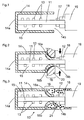
- the housing 14 is here as a sleeve, which is closed in particular on one end face 14a and open on the other end face 14b, executed, other housing forms are conceivable.
- a printed circuit board 11 equipped with the schematically illustrated electronic components 13 and an electrical connection 17, which is embodied concretely as a likewise schematically illustrated plug connection to the wires 18 of a terminating cable 19.
- electrical connection 17 which is embodied concretely as a likewise schematically illustrated plug connection to the wires 18 of a terminating cable 19.
- other types of connections in particular a solder contact to wires of a connection cable, also possible.
- the equipped with the electronic components 13 End portion of the assembled printed circuit board is inserted into the interior 15 of the housing 14.
- FIG. 2 intermediate production shown differs from the above with reference to the FIG. 1 discussed intermediate stage in that with a mold 20, which in the in FIG. 2 moved by arrows was moved, the portion of the housing 14 on the electrical terminals 12 of the printed circuit board 11 facing side of the housing 14 has been transformed, so that a deformed portion 16, which rests against the printed circuit board (11), has arisen.
- the distance between opposing sides 16a, 16b of the deformed portion 16 of the housing 14 in the direction of extension of the printed circuit board 11 increases from the side facing the terminals 12 of the printed circuit board 11 facing side towards the arranged in the housing 14 end portion monotonous or strictly monotone. Since the pitch of the distance between mutually opposite sides 16a, 16b of the deformed portion 16 of the housing 14 in the direction of extension of the assembled printed circuit board 11, starting from the electrical terminals 12 of the assembled printed circuit board 11 side facing towards the arranged in the housing 14 end portion monotonous or strictly monotonous, creates a deformed portion 16, the inward, ie towards the printed circuit board 11 towards a buckle and outwards, i. away in the direction of the assembled printed circuit board 11, has a concave surface contour.
- the embodiment according to the invention of a sensor arrangement 10, which in FIG. 3 is shown proceeds from the intermediate stage by encapsulation with a thermoplastic material 21.
- the overmolded region of the sensor arrangement 10 extends from the deformed section 16 of the housing 14 to the connection cable 19 and therefore protects the connections of the sensor arrangement 10. Because the thermoplastic material 21 shrinks after injection, the sealing effect of the deformed section 16 still remains improved, wherein in addition also a better adhesion between the housing 14 and thermoplastic material 21 is achieved by the geometric configuration of the deformed portion 16 of the housing 14.
Claims (7)
- Agencement capteur (10) avec une carte à circuits équipée de composants (1), avec des raccords électriques (12), dans lequel au moins un composant électronique (13) agencé sur la carte à circuits équipée (11) ou une combinaison de composants électroniques (13) agencés sur la carte à circuits équipée (11) forme(nt) un capteur, et comprenant un boîtier (14) dans la chambre intérieure duquel (15) est agencée au moins une portion terminale de la carte à circuits équipée (11),
caractérisé en ce qu'au moins une portion conformée (16) du boîtier (14) est présente sur le côté du boîtier (14) tourné vers les raccords électriques (12) de la carte à circuits équipée (11), et la portion conformée (16) est conformée de telle manière qu'elle s'applique de façon étanche sur la carte à circuits équipée (11), et l'agencement capteur est enrobé dans une région depuis la portion conformée (16) du boîtier (14) jusqu'au câble de raccordement (19). - Agencement capteur (10) selon la revendication 1,
caractérisé en ce que le boîtier (14) est en un matériau thermoplastique. - Agencement capteur (10) selon la revendication 1 ou 2,
caractérisé en ce que, dans la portion conformée (16) du boîtier (14), la distance entre des côtés (16a, 16b) mutuellement opposés de la portion conformée (16) du boîtier (14) augmente, dans la direction d'extension de la carte à circuits équipée (11), en partant du côté tourné vers les raccords (12) de la carte à circuits équipés (11) jusqu'à son tronçon terminal agencé dans le boîtier (14), de manière monotone ou strictement monotone. - Agencement capteur (10) selon la revendication 3,
caractérisé en ce que la portion conformée (16) du boîtier (14) forme une collerette de forme conique. - Agencement capteur (10) selon la revendication 3,
caractérisé en ce que le gradient de la distance entre des côtés mutuellement opposés (16a, 16b) de la portion conformée (16) du boîtier (14) dans la direction d'extension de la carte à circuits équipés (11) augmente en partant du côté tourné vers les raccords (12) de la carte à circuits équipée (11) jusqu'à son tronçon terminal agencé dans le boîtier (14), de manière monotone ou strictement monotone. - Agencement capteur (10) selon l'une des revendications précédentes,
caractérisé en ce que la portion conformée (16) du boîtier (14) est conformée à la presse axialement depuis le haut, radialement en deux ou en plusieurs parties, ou suivant une combinaison de ces variantes. - Procédé pour la fabrication d'un agencement capteur (10) selon l'une des revendications 1 à 6,
caractérisé en ce que la portion conformée (16) du boîtier (14) est conformée avec un moule chauffé.
Applications Claiming Priority (1)
| Application Number | Priority Date | Filing Date | Title |
|---|---|---|---|
| DE201210108147 DE102012108147A1 (de) | 2012-09-03 | 2012-09-03 | Sensoranordnung |
Publications (3)
| Publication Number | Publication Date |
|---|---|
| EP2704544A2 EP2704544A2 (fr) | 2014-03-05 |
| EP2704544A3 EP2704544A3 (fr) | 2015-01-14 |
| EP2704544B1 true EP2704544B1 (fr) | 2016-02-03 |
Family
ID=48918254
Family Applications (1)
| Application Number | Title | Priority Date | Filing Date |
|---|---|---|---|
| EP13178922.4A Active EP2704544B1 (fr) | 2012-09-03 | 2013-08-01 | Dispositif de détection |
Country Status (2)
| Country | Link |
|---|---|
| EP (1) | EP2704544B1 (fr) |
| DE (1) | DE102012108147A1 (fr) |
Cited By (2)
| Publication number | Priority date | Publication date | Assignee | Title |
|---|---|---|---|---|
| DE102015217572B3 (de) * | 2015-09-15 | 2017-03-16 | Conti Temic Microelectronic Gmbh | Mediendichtes Steuergerät für ein Kraftfahrzeug |
| DE102015217576A1 (de) * | 2015-09-15 | 2017-03-16 | Conti Temic Microelectronic Gmbh | Mediendichtes Steuergerät für ein Kraftfahrzeug und Verfahren zur Herstellung des Steuergerätes |
Families Citing this family (2)
| Publication number | Priority date | Publication date | Assignee | Title |
|---|---|---|---|---|
| DE102014113078B4 (de) * | 2014-09-11 | 2018-05-03 | Borgwarner Ludwigsburg Gmbh | Zündspule und Verfahren zur Herstellung einer Zündspule |
| DE102015225159A1 (de) * | 2015-12-14 | 2017-06-14 | Continental Automotive Gmbh | Magnetfeldsensor mit einem Steckersockel |
Family Cites Families (8)
| Publication number | Priority date | Publication date | Assignee | Title |
|---|---|---|---|---|
| DE2952297A1 (de) * | 1979-12-24 | 1981-07-02 | Werner Dipl.-Ing. 6840 Lampertheim Schaller | Verfahren und vorrichtung zur herstellung von elektronischen geraeten, insbesondere beruehrungslosen sensoren und modulen |
| DE19504608C2 (de) * | 1995-02-11 | 2002-03-21 | Balluff Gebhard Feinmech | Positionssensor und Verfahren zur Herstellung desselben |
| DE19803358C2 (de) * | 1998-01-29 | 2000-02-24 | Telefunken Microelectron | Gehäuse zur Aufnahme von Bauelementen |
| DE10121776B4 (de) * | 2001-05-04 | 2006-10-19 | Sick Ag | Sensor |
| DE202008013766U1 (de) * | 2008-11-10 | 2009-01-08 | Lear Corporation Gmbh | Gehäuse zur Aufnahme mindestens einer mit Bauelementen bestückten Leiterplatte |
| DE102009040915A1 (de) * | 2009-09-10 | 2011-04-07 | Continental Automotive Gmbh | Verfahren zum Verbinden von Gehäuseteilen |
| DE102009060872A1 (de) * | 2009-12-30 | 2011-08-18 | Baumer Innotec Ag | Sensor mit Gehäuse und Verfahren zu dessen Herstellung |
| DE102010062586A1 (de) * | 2010-12-08 | 2012-06-14 | Robert Bosch Gmbh | Elektrische Schaltungsanordnung sowie Verfahren zur Herstellung einer elektrischen Schaltungsanordnung |
-
2012
- 2012-09-03 DE DE201210108147 patent/DE102012108147A1/de not_active Withdrawn
-
2013
- 2013-08-01 EP EP13178922.4A patent/EP2704544B1/fr active Active
Cited By (3)
| Publication number | Priority date | Publication date | Assignee | Title |
|---|---|---|---|---|
| DE102015217572B3 (de) * | 2015-09-15 | 2017-03-16 | Conti Temic Microelectronic Gmbh | Mediendichtes Steuergerät für ein Kraftfahrzeug |
| DE102015217576A1 (de) * | 2015-09-15 | 2017-03-16 | Conti Temic Microelectronic Gmbh | Mediendichtes Steuergerät für ein Kraftfahrzeug und Verfahren zur Herstellung des Steuergerätes |
| DE102015217576B4 (de) | 2015-09-15 | 2017-03-30 | Conti Temic Microelectronic Gmbh | Mediendichtes Steuergerät für ein Kraftfahrzeug und Verfahren zur Herstellung des Steuergerätes |
Also Published As
| Publication number | Publication date |
|---|---|
| DE102012108147A1 (de) | 2014-03-27 |
| EP2704544A3 (fr) | 2015-01-14 |
| EP2704544A2 (fr) | 2014-03-05 |
Similar Documents
| Publication | Publication Date | Title |
|---|---|---|
| EP2027629B1 (fr) | Connecteur enfichable blindé et son procédé de réalisation | |
| EP1699116B1 (fr) | Prise avec membre d'étanchéité pour les contacts sertis et/ou dispositif de retenue de câble | |
| EP3453080B1 (fr) | Connecteur surmoulé | |
| EP2470868B1 (fr) | Système de connexion pour système capteur et système capteur correspondant | |
| EP2704544B1 (fr) | Dispositif de détection | |
| EP2122784B1 (fr) | Ensemble capteur | |
| EP2449581B1 (fr) | Procédé de fabrication d'un composant électronique | |
| EP1199913A2 (fr) | Méthode de fabrication d'unités comprenant une feuille de circuit et un boítier de support | |
| EP1699113A2 (fr) | Connecteur électrique | |
| EP2767807B1 (fr) | Fixation de câble pour boîtier de capteur | |
| EP1170110A1 (fr) | Procédé pour fabriquer une structure conductrice surmoulée en matière plastique d'une unité de circuit électrique ainsi qu'une unité de circuit électrique comprenant une structure conductrice surmoulée en matière plastique | |
| EP2742284B1 (fr) | Dispositif électrique pourvu d'un élément d'étanchéité, élément d'étanchéité pour un dispositif électrique et procédé pour rendre étanche un boîtier | |
| DE19719436C2 (de) | Spritzgußgehäuse | |
| DE102013215365A1 (de) | Elektrische Getriebesteuervorrichtung und Herstellungsverfahren | |
| EP3681689A1 (fr) | Surface structurée par laser pour une liaison par injection de la surface | |
| DE202012103343U1 (de) | Sensoranordnung | |
| EP3503307A1 (fr) | Élément d'accouplement électrique et élément d'étanchéité | |
| DE102006014951B3 (de) | Pinschutz | |
| WO2013178212A2 (fr) | Support pour composant de véhicule à moteur et procédé de fabrication dudit support | |
| EP2243342B1 (fr) | Composant électronique et procédé pour fabriquer un composant électronique | |
| EP3382825B1 (fr) | Étanchéification lors du moulage par injection sur un assemblage par soudure entre des contacts de douille et un grillage estampé | |
| EP0392398B1 (fr) | Méthode pour produire et envelopper des minifusibles et microfusibles | |
| EP1365487B1 (fr) | Procédé de fabrication d'un boîtier | |
| EP3685124A1 (fr) | Support pour une unité de détection | |
| DE102018210621A1 (de) | Elektronikmodul mit Steckeranschluss |
Legal Events
| Date | Code | Title | Description |
|---|---|---|---|
| AK | Designated contracting states |
Kind code of ref document: A2 Designated state(s): AL AT BE BG CH CY CZ DE DK EE ES FI FR GB GR HR HU IE IS IT LI LT LU LV MC MK MT NL NO PL PT RO RS SE SI SK SM TR |
|
| AX | Request for extension of the european patent |
Extension state: BA ME |
|
| PUAI | Public reference made under article 153(3) epc to a published international application that has entered the european phase |
Free format text: ORIGINAL CODE: 0009012 |
|
| PUAL | Search report despatched |
Free format text: ORIGINAL CODE: 0009013 |
|
| AK | Designated contracting states |
Kind code of ref document: A3 Designated state(s): AL AT BE BG CH CY CZ DE DK EE ES FI FR GB GR HR HU IE IS IT LI LT LU LV MC MK MT NL NO PL PT RO RS SE SI SK SM TR |
|
| AX | Request for extension of the european patent |
Extension state: BA ME |
|
| RIC1 | Information provided on ipc code assigned before grant |
Ipc: G01D 11/24 20060101ALI20141205BHEP Ipc: H05K 5/06 20060101AFI20141205BHEP Ipc: H03K 17/95 20060101ALI20141205BHEP Ipc: G01P 1/02 20060101ALI20141205BHEP |
|
| 17P | Request for examination filed |
Effective date: 20150701 |
|
| RBV | Designated contracting states (corrected) |
Designated state(s): AL AT BE BG CH CY CZ DE DK EE ES FI FR GB GR HR HU IE IS IT LI LT LU LV MC MK MT NL NO PL PT RO RS SE SI SK SM TR |
|
| GRAP | Despatch of communication of intention to grant a patent |
Free format text: ORIGINAL CODE: EPIDOSNIGR1 |
|
| RIC1 | Information provided on ipc code assigned before grant |
Ipc: G01D 11/24 20060101ALI20150901BHEP Ipc: G01P 1/02 20060101ALI20150901BHEP Ipc: H03K 17/95 20060101ALI20150901BHEP Ipc: H05K 5/06 20060101AFI20150901BHEP |
|
| INTG | Intention to grant announced |
Effective date: 20151006 |
|
| GRAS | Grant fee paid |
Free format text: ORIGINAL CODE: EPIDOSNIGR3 |
|
| GRAA | (expected) grant |
Free format text: ORIGINAL CODE: 0009210 |
|
| AK | Designated contracting states |
Kind code of ref document: B1 Designated state(s): AL AT BE BG CH CY CZ DE DK EE ES FI FR GB GR HR HU IE IS IT LI LT LU LV MC MK MT NL NO PL PT RO RS SE SI SK SM TR |
|
| REG | Reference to a national code |
Ref country code: GB Ref legal event code: FG4D Free format text: NOT ENGLISH |
|
| REG | Reference to a national code |
Ref country code: AT Ref legal event code: REF Ref document number: 774184 Country of ref document: AT Kind code of ref document: T Effective date: 20160215 Ref country code: CH Ref legal event code: EP |
|
| REG | Reference to a national code |
Ref country code: IE Ref legal event code: FG4D Free format text: LANGUAGE OF EP DOCUMENT: GERMAN |
|
| REG | Reference to a national code |
Ref country code: DE Ref legal event code: R096 Ref document number: 502013001883 Country of ref document: DE |
|
| REG | Reference to a national code |
Ref country code: LT Ref legal event code: MG4D Ref country code: NL Ref legal event code: MP Effective date: 20160203 |
|
| PG25 | Lapsed in a contracting state [announced via postgrant information from national office to epo] |
Ref country code: NO Free format text: LAPSE BECAUSE OF FAILURE TO SUBMIT A TRANSLATION OF THE DESCRIPTION OR TO PAY THE FEE WITHIN THE PRESCRIBED TIME-LIMIT Effective date: 20160503 Ref country code: ES Free format text: LAPSE BECAUSE OF FAILURE TO SUBMIT A TRANSLATION OF THE DESCRIPTION OR TO PAY THE FEE WITHIN THE PRESCRIBED TIME-LIMIT Effective date: 20160203 Ref country code: FI Free format text: LAPSE BECAUSE OF FAILURE TO SUBMIT A TRANSLATION OF THE DESCRIPTION OR TO PAY THE FEE WITHIN THE PRESCRIBED TIME-LIMIT Effective date: 20160203 Ref country code: GR Free format text: LAPSE BECAUSE OF FAILURE TO SUBMIT A TRANSLATION OF THE DESCRIPTION OR TO PAY THE FEE WITHIN THE PRESCRIBED TIME-LIMIT Effective date: 20160504 Ref country code: IT Free format text: LAPSE BECAUSE OF FAILURE TO SUBMIT A TRANSLATION OF THE DESCRIPTION OR TO PAY THE FEE WITHIN THE PRESCRIBED TIME-LIMIT Effective date: 20160203 Ref country code: HR Free format text: LAPSE BECAUSE OF FAILURE TO SUBMIT A TRANSLATION OF THE DESCRIPTION OR TO PAY THE FEE WITHIN THE PRESCRIBED TIME-LIMIT Effective date: 20160203 |
|
| PG25 | Lapsed in a contracting state [announced via postgrant information from national office to epo] |
Ref country code: PL Free format text: LAPSE BECAUSE OF FAILURE TO SUBMIT A TRANSLATION OF THE DESCRIPTION OR TO PAY THE FEE WITHIN THE PRESCRIBED TIME-LIMIT Effective date: 20160203 Ref country code: IS Free format text: LAPSE BECAUSE OF FAILURE TO SUBMIT A TRANSLATION OF THE DESCRIPTION OR TO PAY THE FEE WITHIN THE PRESCRIBED TIME-LIMIT Effective date: 20160603 Ref country code: LT Free format text: LAPSE BECAUSE OF FAILURE TO SUBMIT A TRANSLATION OF THE DESCRIPTION OR TO PAY THE FEE WITHIN THE PRESCRIBED TIME-LIMIT Effective date: 20160203 Ref country code: PT Free format text: LAPSE BECAUSE OF FAILURE TO SUBMIT A TRANSLATION OF THE DESCRIPTION OR TO PAY THE FEE WITHIN THE PRESCRIBED TIME-LIMIT Effective date: 20160603 Ref country code: LV Free format text: LAPSE BECAUSE OF FAILURE TO SUBMIT A TRANSLATION OF THE DESCRIPTION OR TO PAY THE FEE WITHIN THE PRESCRIBED TIME-LIMIT Effective date: 20160203 Ref country code: SE Free format text: LAPSE BECAUSE OF FAILURE TO SUBMIT A TRANSLATION OF THE DESCRIPTION OR TO PAY THE FEE WITHIN THE PRESCRIBED TIME-LIMIT Effective date: 20160203 Ref country code: NL Free format text: LAPSE BECAUSE OF FAILURE TO SUBMIT A TRANSLATION OF THE DESCRIPTION OR TO PAY THE FEE WITHIN THE PRESCRIBED TIME-LIMIT Effective date: 20160203 Ref country code: RS Free format text: LAPSE BECAUSE OF FAILURE TO SUBMIT A TRANSLATION OF THE DESCRIPTION OR TO PAY THE FEE WITHIN THE PRESCRIBED TIME-LIMIT Effective date: 20160203 |
|
| PG25 | Lapsed in a contracting state [announced via postgrant information from national office to epo] |
Ref country code: EE Free format text: LAPSE BECAUSE OF FAILURE TO SUBMIT A TRANSLATION OF THE DESCRIPTION OR TO PAY THE FEE WITHIN THE PRESCRIBED TIME-LIMIT Effective date: 20160203 Ref country code: DK Free format text: LAPSE BECAUSE OF FAILURE TO SUBMIT A TRANSLATION OF THE DESCRIPTION OR TO PAY THE FEE WITHIN THE PRESCRIBED TIME-LIMIT Effective date: 20160203 |
|
| REG | Reference to a national code |
Ref country code: DE Ref legal event code: R097 Ref document number: 502013001883 Country of ref document: DE |
|
| PG25 | Lapsed in a contracting state [announced via postgrant information from national office to epo] |
Ref country code: SM Free format text: LAPSE BECAUSE OF FAILURE TO SUBMIT A TRANSLATION OF THE DESCRIPTION OR TO PAY THE FEE WITHIN THE PRESCRIBED TIME-LIMIT Effective date: 20160203 Ref country code: SK Free format text: LAPSE BECAUSE OF FAILURE TO SUBMIT A TRANSLATION OF THE DESCRIPTION OR TO PAY THE FEE WITHIN THE PRESCRIBED TIME-LIMIT Effective date: 20160203 Ref country code: RO Free format text: LAPSE BECAUSE OF FAILURE TO SUBMIT A TRANSLATION OF THE DESCRIPTION OR TO PAY THE FEE WITHIN THE PRESCRIBED TIME-LIMIT Effective date: 20160203 Ref country code: CZ Free format text: LAPSE BECAUSE OF FAILURE TO SUBMIT A TRANSLATION OF THE DESCRIPTION OR TO PAY THE FEE WITHIN THE PRESCRIBED TIME-LIMIT Effective date: 20160203 |
|
| PLBE | No opposition filed within time limit |
Free format text: ORIGINAL CODE: 0009261 |
|
| STAA | Information on the status of an ep patent application or granted ep patent |
Free format text: STATUS: NO OPPOSITION FILED WITHIN TIME LIMIT |
|
| PG25 | Lapsed in a contracting state [announced via postgrant information from national office to epo] |
Ref country code: BE Free format text: LAPSE BECAUSE OF NON-PAYMENT OF DUE FEES Effective date: 20160831 |
|
| 26N | No opposition filed |
Effective date: 20161104 |
|
| PG25 | Lapsed in a contracting state [announced via postgrant information from national office to epo] |
Ref country code: SI Free format text: LAPSE BECAUSE OF FAILURE TO SUBMIT A TRANSLATION OF THE DESCRIPTION OR TO PAY THE FEE WITHIN THE PRESCRIBED TIME-LIMIT Effective date: 20160203 Ref country code: BG Free format text: LAPSE BECAUSE OF FAILURE TO SUBMIT A TRANSLATION OF THE DESCRIPTION OR TO PAY THE FEE WITHIN THE PRESCRIBED TIME-LIMIT Effective date: 20160503 |
|
| PG25 | Lapsed in a contracting state [announced via postgrant information from national office to epo] |
Ref country code: MC Free format text: LAPSE BECAUSE OF FAILURE TO SUBMIT A TRANSLATION OF THE DESCRIPTION OR TO PAY THE FEE WITHIN THE PRESCRIBED TIME-LIMIT Effective date: 20160203 |
|
| REG | Reference to a national code |
Ref country code: FR Ref legal event code: ST Effective date: 20170428 |
|
| REG | Reference to a national code |
Ref country code: IE Ref legal event code: MM4A |
|
| PG25 | Lapsed in a contracting state [announced via postgrant information from national office to epo] |
Ref country code: IE Free format text: LAPSE BECAUSE OF NON-PAYMENT OF DUE FEES Effective date: 20160801 Ref country code: FR Free format text: LAPSE BECAUSE OF NON-PAYMENT OF DUE FEES Effective date: 20160831 |
|
| PG25 | Lapsed in a contracting state [announced via postgrant information from national office to epo] |
Ref country code: LU Free format text: LAPSE BECAUSE OF NON-PAYMENT OF DUE FEES Effective date: 20160801 |
|
| GBPC | Gb: european patent ceased through non-payment of renewal fee |
Effective date: 20170801 |
|
| PG25 | Lapsed in a contracting state [announced via postgrant information from national office to epo] |
Ref country code: HU Free format text: LAPSE BECAUSE OF FAILURE TO SUBMIT A TRANSLATION OF THE DESCRIPTION OR TO PAY THE FEE WITHIN THE PRESCRIBED TIME-LIMIT; INVALID AB INITIO Effective date: 20130801 Ref country code: CY Free format text: LAPSE BECAUSE OF FAILURE TO SUBMIT A TRANSLATION OF THE DESCRIPTION OR TO PAY THE FEE WITHIN THE PRESCRIBED TIME-LIMIT Effective date: 20160203 |
|
| PG25 | Lapsed in a contracting state [announced via postgrant information from national office to epo] |
Ref country code: MK Free format text: LAPSE BECAUSE OF FAILURE TO SUBMIT A TRANSLATION OF THE DESCRIPTION OR TO PAY THE FEE WITHIN THE PRESCRIBED TIME-LIMIT Effective date: 20160203 Ref country code: MT Free format text: LAPSE BECAUSE OF FAILURE TO SUBMIT A TRANSLATION OF THE DESCRIPTION OR TO PAY THE FEE WITHIN THE PRESCRIBED TIME-LIMIT Effective date: 20160203 Ref country code: TR Free format text: LAPSE BECAUSE OF FAILURE TO SUBMIT A TRANSLATION OF THE DESCRIPTION OR TO PAY THE FEE WITHIN THE PRESCRIBED TIME-LIMIT Effective date: 20160203 |
|
| PG25 | Lapsed in a contracting state [announced via postgrant information from national office to epo] |
Ref country code: GB Free format text: LAPSE BECAUSE OF NON-PAYMENT OF DUE FEES Effective date: 20170801 |
|
| PG25 | Lapsed in a contracting state [announced via postgrant information from national office to epo] |
Ref country code: AL Free format text: LAPSE BECAUSE OF FAILURE TO SUBMIT A TRANSLATION OF THE DESCRIPTION OR TO PAY THE FEE WITHIN THE PRESCRIBED TIME-LIMIT Effective date: 20160203 |
|
| REG | Reference to a national code |
Ref country code: AT Ref legal event code: MM01 Ref document number: 774184 Country of ref document: AT Kind code of ref document: T Effective date: 20180801 |
|
| PG25 | Lapsed in a contracting state [announced via postgrant information from national office to epo] |
Ref country code: AT Free format text: LAPSE BECAUSE OF NON-PAYMENT OF DUE FEES Effective date: 20180801 |
|
| PGFP | Annual fee paid to national office [announced via postgrant information from national office to epo] |
Ref country code: CH Payment date: 20230902 Year of fee payment: 11 |
|
| PGFP | Annual fee paid to national office [announced via postgrant information from national office to epo] |
Ref country code: DE Payment date: 20230822 Year of fee payment: 11 |