EP2699064A2 - Planar based RF sensor technology - Google Patents
Planar based RF sensor technology Download PDFInfo
- Publication number
- EP2699064A2 EP2699064A2 EP13180591.3A EP13180591A EP2699064A2 EP 2699064 A2 EP2699064 A2 EP 2699064A2 EP 13180591 A EP13180591 A EP 13180591A EP 2699064 A2 EP2699064 A2 EP 2699064A2
- Authority
- EP
- European Patent Office
- Prior art keywords
- sensor pads
- vias
- traces
- sensor
- pcb
- Prior art date
- Legal status (The legal status is an assumption and is not a legal conclusion. Google has not performed a legal analysis and makes no representation as to the accuracy of the status listed.)
- Withdrawn
Links
Images



Classifications
-
- G—PHYSICS
- G01—MEASURING; TESTING
- G01R—MEASURING ELECTRIC VARIABLES; MEASURING MAGNETIC VARIABLES
- G01R15/00—Details of measuring arrangements of the types provided for in groups G01R17/00 - G01R29/00, G01R33/00 - G01R33/26 or G01R35/00
- G01R15/14—Adaptations providing voltage or current isolation, e.g. for high-voltage or high-current networks
- G01R15/18—Adaptations providing voltage or current isolation, e.g. for high-voltage or high-current networks using inductive devices, e.g. transformers
-
- G—PHYSICS
- G01—MEASURING; TESTING
- G01R—MEASURING ELECTRIC VARIABLES; MEASURING MAGNETIC VARIABLES
- G01R15/00—Details of measuring arrangements of the types provided for in groups G01R17/00 - G01R29/00, G01R33/00 - G01R33/26 or G01R35/00
- G01R15/14—Adaptations providing voltage or current isolation, e.g. for high-voltage or high-current networks
- G01R15/18—Adaptations providing voltage or current isolation, e.g. for high-voltage or high-current networks using inductive devices, e.g. transformers
- G01R15/181—Adaptations providing voltage or current isolation, e.g. for high-voltage or high-current networks using inductive devices, e.g. transformers using coils without a magnetic core, e.g. Rogowski coils
-
- G—PHYSICS
- G01—MEASURING; TESTING
- G01R—MEASURING ELECTRIC VARIABLES; MEASURING MAGNETIC VARIABLES
- G01R19/00—Arrangements for measuring currents or voltages or for indicating presence or sign thereof
-
- G—PHYSICS
- G01—MEASURING; TESTING
- G01R—MEASURING ELECTRIC VARIABLES; MEASURING MAGNETIC VARIABLES
- G01R19/00—Arrangements for measuring currents or voltages or for indicating presence or sign thereof
- G01R19/0092—Measuring current only
-
- G—PHYSICS
- G01—MEASURING; TESTING
- G01R—MEASURING ELECTRIC VARIABLES; MEASURING MAGNETIC VARIABLES
- G01R23/00—Arrangements for measuring frequencies; Arrangements for analysing frequency spectra
- G01R23/02—Arrangements for measuring frequency, e.g. pulse repetition rate; Arrangements for measuring period of current or voltage
-
- G—PHYSICS
- G01—MEASURING; TESTING
- G01R—MEASURING ELECTRIC VARIABLES; MEASURING MAGNETIC VARIABLES
- G01R29/00—Arrangements for measuring or indicating electric quantities not covered by groups G01R19/00 - G01R27/00
- G01R29/08—Measuring electromagnetic field characteristics
-
- H—ELECTRICITY
- H01—ELECTRIC ELEMENTS
- H01F—MAGNETS; INDUCTANCES; TRANSFORMERS; SELECTION OF MATERIALS FOR THEIR MAGNETIC PROPERTIES
- H01F27/00—Details of transformers or inductances, in general
- H01F27/28—Coils; Windings; Conductive connections
- H01F27/2804—Printed windings
-
- H—ELECTRICITY
- H01—ELECTRIC ELEMENTS
- H01F—MAGNETS; INDUCTANCES; TRANSFORMERS; SELECTION OF MATERIALS FOR THEIR MAGNETIC PROPERTIES
- H01F38/00—Adaptations of transformers or inductances for specific applications or functions
- H01F38/20—Instruments transformers
- H01F38/22—Instruments transformers for single phase AC
- H01F38/28—Current transformers
- H01F38/30—Constructions
-
- H—ELECTRICITY
- H05—ELECTRIC TECHNIQUES NOT OTHERWISE PROVIDED FOR
- H05H—PLASMA TECHNIQUE; PRODUCTION OF ACCELERATED ELECTRICALLY-CHARGED PARTICLES OR OF NEUTRONS; PRODUCTION OR ACCELERATION OF NEUTRAL MOLECULAR OR ATOMIC BEAMS
- H05H1/00—Generating plasma; Handling plasma
- H05H1/24—Generating plasma
- H05H1/46—Generating plasma using applied electromagnetic fields, e.g. high frequency or microwave energy
-
- H—ELECTRICITY
- H05—ELECTRIC TECHNIQUES NOT OTHERWISE PROVIDED FOR
- H05H—PLASMA TECHNIQUE; PRODUCTION OF ACCELERATED ELECTRICALLY-CHARGED PARTICLES OR OF NEUTRONS; PRODUCTION OR ACCELERATION OF NEUTRAL MOLECULAR OR ATOMIC BEAMS
- H05H1/00—Generating plasma; Handling plasma
- H05H1/24—Generating plasma
- H05H1/46—Generating plasma using applied electromagnetic fields, e.g. high frequency or microwave energy
- H05H1/4645—Radiofrequency discharges
-
- H—ELECTRICITY
- H01—ELECTRIC ELEMENTS
- H01F—MAGNETS; INDUCTANCES; TRANSFORMERS; SELECTION OF MATERIALS FOR THEIR MAGNETIC PROPERTIES
- H01F38/00—Adaptations of transformers or inductances for specific applications or functions
- H01F38/20—Instruments transformers
- H01F38/22—Instruments transformers for single phase AC
- H01F38/28—Current transformers
- H01F38/30—Constructions
- H01F2038/305—Constructions with toroidal magnetic core
-
- H—ELECTRICITY
- H05—ELECTRIC TECHNIQUES NOT OTHERWISE PROVIDED FOR
- H05H—PLASMA TECHNIQUE; PRODUCTION OF ACCELERATED ELECTRICALLY-CHARGED PARTICLES OR OF NEUTRONS; PRODUCTION OR ACCELERATION OF NEUTRAL MOLECULAR OR ATOMIC BEAMS
- H05H2242/00—Auxiliary systems
- H05H2242/20—Power circuits
-
- H—ELECTRICITY
- H05—ELECTRIC TECHNIQUES NOT OTHERWISE PROVIDED FOR
- H05H—PLASMA TECHNIQUE; PRODUCTION OF ACCELERATED ELECTRICALLY-CHARGED PARTICLES OR OF NEUTRONS; PRODUCTION OR ACCELERATION OF NEUTRAL MOLECULAR OR ATOMIC BEAMS
- H05H2242/00—Auxiliary systems
- H05H2242/20—Power circuits
- H05H2242/24—Radiofrequency or microwave generators
Definitions
- the present disclosure relates to radio frequency sensors and, more particularly, to a radio frequency (RF) sensor system comprising an orthogonal radio frequency voltage/current sensor and associated method.
- RF radio frequency
- a radio frequency (RF) current sensor which is also known as a probe, generates a signal that represents the magnitude of current flow through an RF conductor.
- the current probe can be combined with a voltage probe to form an RF voltage/current (VI) probe that generates a second signal that represents the RF voltage with respect to a reference potential, such as an RF ground or shield conductor.
- V RF voltage/current
- RF current and VI probes are used in RF control circuits to provide feedback information.
- the feedback information may be used to control an RF amplifier that provides the RF power that is being measured.
- the RF power is employed to generate plasma for semiconductor manufacturing, metal coating, or micromachining processes.
- a radio frequency (RF) sensor system comprising: a printed circuit board (PCB) including a first exterior layer, a second exterior layer, a first interior layer, a second interior layer, and an inner perimeter that defines an aperture through the PCB; a first loop comprising a first plurality of sensor pads coupled to a first plurality of vias by a first plurality of traces, the first plurality of sensor pads being arranged on the inner perimeter; a second loop comprising a second plurality of sensor pads coupled to a second plurality of vias by a second plurality of traces, the second plurality of sensor pads being arranged on the inner perimeter; and a core ring embedded within the first interior layer proximal to the first plurality of sensor pads, the first plurality of vias, and the first plurality of traces; wherein a center conductor for carrying RF current extends through the aperture and the first and second loops generate an electrical signal based on the first and second plurality of sensor pads, the first and second
- the core ring consists of a medium with a greater permeability than air.
- the core ring consists of a ferromagnetic material.
- the core ring has a coefficient of thermal expansion equal to the coefficient of expansion of the first and second exterior layers and the first and second interior layers.
- the core ring has a coefficient of thermal expansion of less than the coefficient of expansion of the first and second exterior layers and the first and second interior layers.
- At least one of a plurality of characteristics of the plurality of vias is selectively adjusted based on a resonance of the RF sensor.
- the RF sensor system further comprises a second PCB including a third exterior layer, a fourth exterior layer, a third interior layer, a fourth interior layer, and an second inner perimeter that defines a second aperture through the second PCB; a third loop comprising a third plurality of sensor pads coupled to a third plurality of vias by a third plurality of traces, the third plurality of sensor pads being arranged on the second inner perimeter; and a fourth loop comprising a fourth plurality of sensor pads coupled to a fourth plurality of vias by a fourth plurality of traces, the fourth plurality of sensor pads being arranged on the second inner perimeter.
- the fourth exterior layer is electrically bound to the first exterior layer.
- the first plurality of sensor pads, the second plurality of sensor pads, third plurality of sensor pads, and the fourth plurality of sensor pads are electronically connected in series.
- the first plurality of sensor pads, the second plurality of sensor pads, third plurality of sensor pads, and the fourth plurality of sensor pads are electronically connected in parallel.
- a radio frequency (RF) sensing method comprising: defining an aperture through a printed circuit board (PCB), wherein the PCB includes a first exterior layer, a second exterior layer, a first interior layer, a second interior layer, and an inner perimeter; coupling a first loop comprising a first plurality of sensor pads to a first plurality of vias by a first plurality of traces, arranging the first plurality of sensor pads on the inner perimeter; coupling a second loop comprising a second plurality of sensor pads to a second plurality of vias by a second plurality of traces, arranging the second plurality of sensor pads on the inner perimeter; and embedding a core ring within the first interior layer proximal to the first plurality of sensor pads, the first plurality of vias, and the first plurality of traces; wherein a center conductor for carrying RF current extends through the aperture and the first and second loops generate an electrical signal based on the first and second plurality of sensor pads,
- the method further comprises selectively adjusting at least one of a plurality of characteristics of the plurality of vias based on a resonance of the RF sensor.
- the method further comprises defining a second aperture a second PCB, wherein the second PCB includes a third exterior layer, a fourth exterior layer, a third interior layer, a fourth interior layer, and a second inner perimeter; coupling a third loop comprising a third plurality of sensor pads to a third plurality of vias by a third plurality of traces, the third plurality of sensor pads being arranged on the second inner perimeter; and coupling a fourth loop comprising a fourth plurality of sensor pads to a fourth plurality of vias by a fourth plurality of traces, the fourth plurality of sensor pads being arranged on the second inner perimeter.
- the method further comprises electrically binding the fourth exterior layer to the first exterior layer.
- the method further comprises electrically connecting in series the first plurality of sensor pads, the second plurality of sensor pads, third plurality of sensor pads, and the fourth plurality of sensor pads.
- the method further comprises electrically connecting in parallel the first plurality of sensor pads, the second plurality of sensor pads, third plurality of sensor pads, and the fourth plurality of sensor pads.
- a radio frequency sensor system includes a printed circuit board (PCB) is provided.
- the PCB includes a first exterior layer, a second exterior layer, a first interior layer, a second interior layer, and an inner perimeter that defines an aperture through the PCB.
- the PCB also includes a first loop.
- the first loop includes a first plurality of sensor pads coupled to a first plurality of vias by a first plurality of traces.
- the first plurality of sensor pads is arranged on the inner perimeter.
- the PCB also includes a second loop.
- the second loop includes a second plurality of sensor pads coupled to a second plurality of vias by a second plurality of traces.
- the second plurality of sensor pads is arranged on the inner perimeter.
- a core ring is embedded within the first interior layer proximal to the first plurality of sensor pads, the first plurality of vias, and the first plurality of traces.
- a center conductor, for carrying RF current, extends through the aperture.
- the first and second loops generate an electrical signal based on the first and second plurality of sensor pads, the first and second plurality of vias, the first and second plurality of traces, and the core ring.
- a radio frequency sensing method includes defining an aperture through a printed circuit board (PCB).
- the PCB includes a first exterior layer, a second exterior layer, a first interior layer, a second interior layer, and an inner perimeter.
- the first loop includes a first plurality of sensor pads. Arranging the first plurality of sensor pads on the inner perimeter.
- the second loop includes a second plurality of sensor pads. Arranging the second plurality of sensor pads on the inner perimeter.
- a center conductor for carrying RF current extends through the aperture and the first and second loops generate an electrical signal based on the first and second plurality of sensor pads, the first and second plurality of vias, the first and second plurality of traces, and the core ring.
- the invention also provides a computer program and a computer program product for carrying out any of the methods described herein, and/or for embodying any of the apparatus features described herein, and a computer readable medium having stored thereon a program for carrying out any of the methods described herein and/or for embodying any of the apparatus features described herein.
- the invention also provides a signal embodying a computer program for carrying out any of the methods described herein, and/or for embodying any of the apparatus features described herein, a method of transmitting such a signal, and a computer product having an operating system which supports a computer program for carrying out the methods described herein and/or for embodying any of the apparatus features described herein.
- a radio frequency (RF) current sensor which is also known as a probe, generates a signal that represents the magnitude of current flow through an RF conductor.
- the current probe can be combined with a voltage probe to form an RF voltage/current (VI) probe that generates a second signal that represents the RF voltage with respect to a reference potential, such as an RF ground or shield conductor.
- V RF voltage/current
- RF current and VI probes are used in RF control circuits to provide feedback information.
- the feedback information may be used to control an RF amplifier that provides the RF power that is being measured.
- the RF power is employed to generate plasma for semiconductor manufacturing, metal coating, or micromachining processes.
- the VI probe While operating at certain frequencies, for example low frequencies or high frequencies, the VI probe may experience interference due to parasitic resonance within the components of the VI probe. Additionally, the low frequency coupling of the sensor to the center conductor may be low. Accordingly, the principles of the present disclosure may be arranged to improve VI probe frequency responses.
- VI probe 10 includes a printed circuit board (PCB) 12 with at least four conductive layers.
- a first exterior layer 14a and a second exterior layer 14b are parallel with each other and maintained in spaced relationship by an insulating substrate of the PCB 12.
- First and second layers 14a, 14b are collectively referred to as ground planes 14.
- a number of vias 16 electrically connect ground planes 14 to each other. Vias 16 can be radially spaced around a perimeter of an aperture 18. Vias 16 are electrically insulated from the inner layers of the PCB 12, which are described below.
- Ground planes 14 and vias 16 connect to an outer layer of a coaxial cable (not shown) that carries the RF current being measured.
- a center conductor of the coaxial cable connects to a conductor 20 that is axially and concentrically positioned within aperture 18.
- VI probe 10 may also include a plurality of mounting holes 13 to assist in coupling the VI probe 10 to the RF power generator (not shown) to be controlled.
- a second plurality of vias 22 are electrically insulated from ground planes 14 and connect current loop-back traces that are located on inner layers of the PCB 12.
- a third plurality of vias 24 are also electrically insulated from ground planes 14 and implement part of a voltage sensor H field cancellation structure. Vias 22 and 24 and their associated traces on inner layers of the PCB 12 are described below in more detail.
- the PCB 12 may also include an embedded core ring 42.
- the core ring 42 is embedded in at least one layer of the PCB 12. Further, the core ring 42 is arranged between the vias 22 and 24 and current sensor pads 30.
- the core ring 42 is arranged to increase a magnetic flux of the VI probe 10.
- the core ring 42 comprises material that increases a permeability of a medium in a magnetic field of the VI probe 10.
- the medium in the magnetic field may be comprised of air and the core ring 42 comprises material with a higher permeability than air.
- the core ring 42 may comprise a ferromagnetic material or a ferrimagnetic material.
- the PCB 12 may also include traces and pads, which are generically indicated at 28, for mounting electronic circuit components that may be connected to ground plane 14 and the various traces of the inner layers of the PCB 12.
- components include: connectors for providing power to the electronic circuits and/or taking electrical signals from them, amplifiers, transformers, and/or filters that buffer and/or condition the signals that represent the RF voltage and/or current of conductor 20, and the like.
- a first inner layer 32 includes traces 44a and 44b that are formed on insulating substrate 36.
- a second inner layer 34 includes more traces 44a and 44b on the opposing side of substrate 36. Traces 44a and 44b are collectively referred to as traces 44. Traces 44 are patterned and connected by vias 22 to form a pair of entwined electrical loops or windings.
- substrate 36 may contain one or more additional conductive layers that are not shown. The additional conductive layers may, e.g., implement a voltage sensor that is described below.
- First and second inner layers 32, 34 are positioned underneath and insulated from respective ones of ground planes 14. Vias 22 extend between and connect associated traces 44 on the first and second inner layers as is described below. Associated traces 44 are also connected by respective current sensor pads 30 that are formed along walls of aperture 18. Current sensor pads 30 can be plated to the edge of aperture 18 in substrate 36 and cut to shape by laser, mechanical abrasion or other manufacturing technique.
- Insulator substrate 36 gives current sensor pads 30 a length L. While RF current flows through conductor 20, a magnetic field rotates around conductor 20.
- the magnetic field crosses current sensor pads 30.
- the induced voltage is a function of the length L of current sensor pads 30, a rate of change of the magnetic field, and a height of a loop formed by current sensor pads 30, traces 44, and vias 22.
- Increasing the length L such as by increasing a thickness of substrate 36, increases coupling between the RF coaxial cable (not shown) and VI probe 10.
- the diameter of vias 22 may also need to be increased in order to reduce the risk of breaking drills during PCB 36 fabrication. Increasing the diameter of vias 22 also increases the size of the sensor and/or reduces the number of current sensor pads 30 or loops (described below) that fit along the perimeter of aperture 18. Increasing the diameter of vias 22 also yields a proportional increase to the capacitive coupling to conductor 20, which allows the electric field ("E field") produced by conductor 20 to contaminate the desired current signals and reduce the dynamic range of the VI probe 10. In various embodiments, the width of the current sensor pads 30 may be made as narrow as is practicable to mitigate E field contamination and dynamic range issues. Edge plated current sensor pads 30 reduce the size and number of vias 22 required to make VI probe 10, which reduces E field contamination of the current signal. The current signal represents the current flowing through conductor 20 and is taken from traces 44.
- the dynamic range of the VI probe 10 is increased by increasing the current sensor pad 30 length (L).
- a second PCB 15 may be coupled to the PCB 12 as shown in FIG. 2 .
- the second PCB 15 may be coupled to the PCB 12 with a coupling layer (not show) between the second PCB 15 and the PCB 12.
- the coupling layer consists of a conductive material arranged to electrically bind the second PCB 15 to the PCB 12.
- the coupling layer may consist of copper.
- the current sensor pads 30 may be connected in series from the second PCB15 to the PCB 12.
- the current sensor pads 30 may be connected in parallel from the second PCB 15 and the PCB 12. While only a second PCB 15 is shown coupled to the PCB 12, it is understood that any number of PCBs may be coupled to the PCB 12, for example, a third, fourth, or fifth PCB.
- the dynamic range of the VI probe 10 may be increased by embedding the core ring 42 into the second PCB 15 and the PCB 12.
- the core ring 42 may be embedded between the vias 22 and 24, the current sensor pads 30, and traces 44 on the second PCB 15 and the PCB 12 respectively.
- the core ring 42 is arranged to increase a magnetic flux of the VI probe 10.
- the core ring 42 is made of a material that increases the permeability of the medium in a magnetic field of the VI probe 10. As the permeability of the medium in the magnetic field increases, the related magnetic flux increases. While FIG. 2 shows the core ring 42 embedded on both the second PCB 15 and the PCB 12, it is understood that the core ring 42 may be embedded in either, both, or neither of the second PCB 15 and the PCB 12.
- the dynamic range of the VI probe 10 may be further increased by selectively adjusting the parameters of the vias 22 and 24, the current sensor pads 30, and the traces 44.
- the core ring 42 is encircled by a plurality of windings.
- the plurality of windings is constructed of the vias 22 and 24, the current sensor pads 30, and the traces 44.
- the resonance of the VI probe 10 can be controlled by selectively adjusting the number of windings and/or selectively adjusting the size of the vias 22 and 24, the current sensor pads 30, and the traces 44. By controlling the resonance of the VI probe 10, the dynamic range of the VI probe 10 may be increased.
- Traces 44 are shown in more detail in FIGS. 3(a)-3(c) .
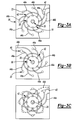
- Traces 44a and traces 44b are connected to form two entwined loops of wire.
- Traces 44a and 44b of FIG. 3(a) connect the current sensor pads 30 to the loop back vias 22.
- the loop back vias 22 connect to the backside of the sensor to another trace 44a or 44b and to the next current sensor pad 30, as shown in FIG. 3(c) .
- FIG. 3 depicts the two loops as traces 44a and 44b.
- the dotted lines are the traces on the back of the board.
- the hexagon 40 of FIG. 3 may be a common ground point for both loops as one of the RF path ground vias 16. This common ground system may be used to reduce ground loops.
- the current loops provide an autocorrecting feature from movement of the conductor 20, such as from assembly/disassembly of VI probe 10 or thermal changes in the VI probe 10 during operation.
- the autocorrecting feature of the design works by maintaining a constant sum total distance from the conductor 20 to the current sensor pads 30. If, for example, the conductor 20 moves to the right, the right current sensor pad 30 to conductor 20 distance decreases, but the left current sensor pad 30 to center conductor 20 increases by the same amount, keeping the sum total distance and current signal level the same.
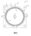
- FIG. 4 Another view of the PCB 12 according to various embodiments of the present disclosure is shown in FIG. 4 .
- Ground planes 14 and vias 16 are omitted for clarity.
- a first inner layer 32 includes traces 44a and 44b that are formed on insulating substrate 36.
- a second inner layer 34 includes more traces 44a and 44b on the opposing side of substrate 36. Traces 44a and 44b are collectively referred to as traces 44. Traces 44 are patterned and connected by vias 22 to form a pair of entwined electrical loops or windings.
- substrate 36 may contain one or more additional conductive layers that are not shown. The additional conductive layers may, e.g., implement a voltage sensor that is described below.
- vias 24 are electrically connected to current sensor pads 30 to implement a voltage sensor in the manner described below (see, for example, FIG. 8 ).
- FIG. 5(a) A schematic representation of a prior art current sensor is illustrated in FIG. 5(a) .
- the circuit of FIG. 5(a) may act as a current sensor with the sensor loops 60 placed end to end (in series) such that there is no coupling between the loops 60.
- FIG. 5(b) A schematic representation of a current sensor according to various embodiments of the present disclosure is illustrated in FIG. 5(b) .
- a common ground is utilized for the loops 60. From Ampere's law, with the RF current traveling into the page, a magnetic field will be generated in a clockwise direction around the conductor 20. The magnetic field will induce a current on the pickup loops 60 to flow through the transformer 50. Any electric fields picked up by the loops 60 will be shorted to ground.
- the circuit of FIG. 5(b) includes two loops 60 next to each other (or parallel to each other) and there is no coupling between the loops 60.
- FIG. 5(c) A schematic representation of a current sensor according to various embodiments of the present disclosure is illustrated in FIG. 5(c) .
- the loops 60 are not connected to a common ground. From Ampere's law, with the RF current traveling into the page, a magnetic field will be generated in a clockwise direction around the conductor 20.
- a resistor 55 in series with each of the two current pick up loops 60 may be included.
- the resistors 55 may be used to match the sensor impedance to any accompanying processing unit that may be utilized with the VI probe 10, which will result in lower reflected signals, lower noise and maximum sensor signal power transfer to the processing unit.
- the magnetic field will induce a current on the pickup loops 60 to flow through the transformer 50 and resistors 55.
- the two current loops 60 will be exposed to the same magnetic and electric fields, which results in better cancellation of the E fields and an increase in the current sensor dynamic range.
- the length of the current sensor pick up lines (for example, current sensor pads 30) is related to the frequency response and coupling of the sensor 10. A longer current sensor pick up will improve signal coupling and the low frequency response of sensor 10, without decreasing the voltage breakdown of the VI probe 10 and other adverse effects.
- the transformer 50 generally has a turn ratio ("N") with respect to the primary and secondary windings.
- the resistors 55 compensate for the real portion of the output impedance.
- the imaginary portion of the output impedance may be compensated for by presenting real transmission line sensor sections or matching/filter circuits.
- FIG. 6 a schematic representation of yet another current sensor according to various embodiments of the present disclosure is illustrated.
- the circuit of FIG. 5(c) is modified by removing the ground and connecting the loops 60 (for example, end-to-end) to form one continuous loop 60. This may be accomplished, for example, by connecting the traces 44a and 44b (as shown in FIGS. 3(a)-3(c) ) by a via at the position of the hexagon 40.
- the electric field impinged on the current sensor is not shorted to ground and, therefore, the E field potential will cause current to flow through the series resistors 55.
- the current from the E field will aid in one current loop while reduce the current in the other current loop, which may result in a portion of the E field signal to pass through the transformer 50.
- This E field contamination may reduce the dynamic range of the current sensor.
- a magnetic field will be generated in a clockwise direction around the conductor 20.
- the resistors 55 may be used to match the sensor impedance to any accompanying processing unit that may be utilized with the VI probe 10, which will result in lower reflected signals, lower noise and maximum sensor signal power transfer to the processing unit.
- the magnetic field will induce a current on the pickup loops 60 to flow through the transformer 50 and resistors 55.
- the electric field picked up by loops 60 will not be shorted to ground, as in the case of FIGS. 5(a) and 5(b) .
- the E fields at points A and B on the transformer 50 will be equal, resulting in no current flow through the transformer 50 due to the E field. Therefore, the E field will be effectively canceled on the secondary or output side 57 of the transformer 50.
- points A and B of transformer 50 will be at relatively the same electrical potential.
- the voltage potential at points A and B are proportional to the electric potential in the conductor 20, due to capacitive coupling.
- the voltage potential at points A and B can be thought of as the electrical potential of the conductor 20 plus an additional component due to contamination from the current signals generated on loops 60 by the magnetic field.
- FIG. 7 is a circuit diagram that represents a circuit showing a capacitive coupling relationship between the voltage at points A and B to that of the voltage of the conductor 20 of FIG. 6 .
- the resistor R m is the measurement input impedance, such as in an analog-to-digital converter or receiver; I m represents the current produced by the changing magnetic field around the conductor 20; C c represents the distributed coupling capacitance between the conductor 20 and the current loops 60; and V e is the RF voltage of the conductor 20.
- V A R m ⁇ V e ⁇ s Cc + I m 1 + s Cc ⁇ R m
- V B - R m ⁇ - V e ⁇ s Cc + I m 1 + s Cc ⁇ R m
- V sum V A + V B
- ADC/DSP analog-to-digital converter/digital signal processing
- V diff R m ⁇ V e ⁇ s Cc + I m 1 + s Cc ⁇ R m - - R m ⁇ - V e ⁇ s Cc + I m 1 + s Cc ⁇ R m
- V diff I m ⁇ 2 ⁇ R m 1 + s Cc ⁇ R m
- FIG. 8 A schematic representation of a voltage/current sensor according to various embodiments of the present disclosure is illustrated in FIG. 8 .
- a magnetic field will be generated in a clockwise direction around the conductor 20.
- the magnetic field will induce a current on the pickup loops 60 to flow through the transformer 50.
- the electric field impinged on the voltage/current sensor is not shorted to ground and, therefore, the E field potential will cause current to flow through the series resistors 55.
- the current from the E field will aid in one current loop while reduce the current in the other current loop, which may result in a portion of the E field signal to pass through the transformer 50. This E field contamination may reduce the dynamic range of the current sensor.
- the electrical signal representing the current of the conductor 20 may be obtained from the secondary side 57 of the transformer 50.
- a center tap 59 of the transformer 50 may be utilized to obtain the electrical signal representing the voltage of the conductor 20. From these electrical signals, the voltage and current of the conductor 20 may be determined, e.g., based on the equations set forth above.
- a third inner layer 33 includes a circular conductive ring 102a that is formed on insulating substrate 36.
- a fourth inner layer 35 includes another circular conductive ring 102b on the opposite side of substrate 36.
- Circular conductive rings 102a and 102b are collectively referred to as circular conductive rings 102.
- Circular conductive rings 102 are patterned and connected to each other by vias 24.
- Each of the circular conductive rings 102 defines a plane that is orthogonal to the longitudinal axis of the conductor 20.
- traces 104 couple each of the circular conductive rings 102 to voltage sensor pads 100 that are formed along walls of aperture 18.
- the voltage sensor pads 100 may be the same as the current sensor pads 30 described above. Voltage sensor pads 100 can be plated to the edge of aperture 18 in substrate 36 and cut to shape by laser, mechanical abrasion or other manufacturing technique. Hexagon 40 may be utilized as a reference ground for determining a voltage of the conductor 20.
- the inner layer 33 also includes an embedded core ring 42. The core ring 42 is embedded in the inner layer 33 between circular conductive rings 102a and 102b.
Landscapes
- Engineering & Computer Science (AREA)
- Physics & Mathematics (AREA)
- Power Engineering (AREA)
- General Physics & Mathematics (AREA)
- Plasma & Fusion (AREA)
- Electromagnetism (AREA)
- Spectroscopy & Molecular Physics (AREA)
- Measuring Instrument Details And Bridges, And Automatic Balancing Devices (AREA)
- Production Of Multi-Layered Print Wiring Board (AREA)
Abstract
Description
- The present disclosure relates to radio frequency sensors and, more particularly, to a radio frequency (RF) sensor system comprising an orthogonal radio frequency voltage/current sensor and associated method.
- A radio frequency (RF) current sensor, which is also known as a probe, generates a signal that represents the magnitude of current flow through an RF conductor. The current probe can be combined with a voltage probe to form an RF voltage/current (VI) probe that generates a second signal that represents the RF voltage with respect to a reference potential, such as an RF ground or shield conductor.
- RF current and VI probes are used in RF control circuits to provide feedback information. The feedback information may be used to control an RF amplifier that provides the RF power that is being measured. In some applications the RF power is employed to generate plasma for semiconductor manufacturing, metal coating, or micromachining processes.
- Further areas of applicability of the present disclosure will become apparent from the detailed description provided hereinafter. It should be understood that the detailed description and specific examples are intended for purposes of illustration only and are not intended to limit the scope of the disclosure.
- According to one aspect of the invention, there is provided a radio frequency (RF) sensor system comprising: a printed circuit board (PCB) including a first exterior layer, a second exterior layer, a first interior layer, a second interior layer, and an inner perimeter that defines an aperture through the PCB; a first loop comprising a first plurality of sensor pads coupled to a first plurality of vias by a first plurality of traces, the first plurality of sensor pads being arranged on the inner perimeter; a second loop comprising a second plurality of sensor pads coupled to a second plurality of vias by a second plurality of traces, the second plurality of sensor pads being arranged on the inner perimeter; and a core ring embedded within the first interior layer proximal to the first plurality of sensor pads, the first plurality of vias, and the first plurality of traces; wherein a center conductor for carrying RF current extends through the aperture and the first and second loops generate an electrical signal based on the first and second plurality of sensor pads, the first and second plurality of vias, the first and second plurality of traces, and the core ring.
- Preferably, the core ring consists of a medium with a greater permeability than air.
- Preferably, the core ring consists of a ferromagnetic material.
- Preferably, the core ring has a coefficient of thermal expansion equal to the coefficient of expansion of the first and second exterior layers and the first and second interior layers.
- Preferably, the core ring has a coefficient of thermal expansion of less than the coefficient of expansion of the first and second exterior layers and the first and second interior layers.
- Preferably, at least one of a plurality of characteristics of the plurality of vias is selectively adjusted based on a resonance of the RF sensor.
- Preferably, the RF sensor system further comprises a second PCB including a third exterior layer, a fourth exterior layer, a third interior layer, a fourth interior layer, and an second inner perimeter that defines a second aperture through the second PCB;
a third loop comprising a third plurality of sensor pads coupled to a third plurality of vias by a third plurality of traces, the third plurality of sensor pads being arranged on the second inner perimeter; and a fourth loop comprising a fourth plurality of sensor pads coupled to a fourth plurality of vias by a fourth plurality of traces, the fourth plurality of sensor pads being arranged on the second inner perimeter. - Preferably, the fourth exterior layer is electrically bound to the first exterior layer.
- Preferably, the first plurality of sensor pads, the second plurality of sensor pads, third plurality of sensor pads, and the fourth plurality of sensor pads are electronically connected in series.
- Alternatively, the first plurality of sensor pads, the second plurality of sensor pads, third plurality of sensor pads, and the fourth plurality of sensor pads are electronically connected in parallel.
- According to another aspect of the invention there is provided a radio frequency (RF) sensing method comprising: defining an aperture through a printed circuit board (PCB), wherein the PCB includes a first exterior layer, a second exterior layer, a first interior layer, a second interior layer, and an inner perimeter; coupling a first loop comprising a first plurality of sensor pads to a first plurality of vias by a first plurality of traces, arranging the first plurality of sensor pads on the inner perimeter; coupling a second loop comprising a second plurality of sensor pads to a second plurality of vias by a second plurality of traces, arranging the second plurality of sensor pads on the inner perimeter; and embedding a core ring within the first interior layer proximal to the first plurality of sensor pads, the first plurality of vias, and the first plurality of traces; wherein a center conductor for carrying RF current extends through the aperture and the first and second loops generate an electrical signal based on the first and second plurality of sensor pads, the first and second plurality of vias, the first and second plurality of traces, and the core ring.
- Preferably, the method further comprises selectively adjusting at least one of a plurality of characteristics of the plurality of vias based on a resonance of the RF sensor.
- Preferably, the method further comprises defining a second aperture a second PCB, wherein the second PCB includes a third exterior layer, a fourth exterior layer, a third interior layer, a fourth interior layer, and a second inner perimeter; coupling a third loop comprising a third plurality of sensor pads to a third plurality of vias by a third plurality of traces, the third plurality of sensor pads being arranged on the second inner perimeter; and coupling a fourth loop comprising a fourth plurality of sensor pads to a fourth plurality of vias by a fourth plurality of traces, the fourth plurality of sensor pads being arranged on the second inner perimeter.
- Preferably, the method further comprises electrically binding the fourth exterior layer to the first exterior layer.
- Preferably, the method further comprises electrically connecting in series the first plurality of sensor pads, the second plurality of sensor pads, third plurality of sensor pads, and the fourth plurality of sensor pads.
- Preferably, the method further comprises electrically connecting in parallel the first plurality of sensor pads, the second plurality of sensor pads, third plurality of sensor pads, and the fourth plurality of sensor pads.
- According to some embodiments, a radio frequency sensor system includes a printed circuit board (PCB) is provided. The PCB includes a first exterior layer, a second exterior layer, a first interior layer, a second interior layer, and an inner perimeter that defines an aperture through the PCB. The PCB also includes a first loop. The first loop includes a first plurality of sensor pads coupled to a first plurality of vias by a first plurality of traces. The first plurality of sensor pads is arranged on the inner perimeter. The PCB also includes a second loop. The second loop includes a second plurality of sensor pads coupled to a second plurality of vias by a second plurality of traces. The second plurality of sensor pads is arranged on the inner perimeter. A core ring is embedded within the first interior layer proximal to the first plurality of sensor pads, the first plurality of vias, and the first plurality of traces. A center conductor, for carrying RF current, extends through the aperture. The first and second loops generate an electrical signal based on the first and second plurality of sensor pads, the first and second plurality of vias, the first and second plurality of traces, and the core ring.
- In other features, a radio frequency sensing method includes defining an aperture through a printed circuit board (PCB). The PCB includes a first exterior layer, a second exterior layer, a first interior layer, a second interior layer, and an inner perimeter. Coupling a first loop to a first plurality of vias by a first plurality of traces. The first loop includes a first plurality of sensor pads. Arranging the first plurality of sensor pads on the inner perimeter. Coupling a second loop to a second plurality of vias by a second plurality of traces. The second loop includes a second plurality of sensor pads. Arranging the second plurality of sensor pads on the inner perimeter. Embedding a core ring within the first interior layer proximal to the first plurality of sensor pads, the first plurality of vias, and the first plurality of traces. A center conductor for carrying RF current extends through the aperture and the first and second loops generate an electrical signal based on the first and second plurality of sensor pads, the first and second plurality of vias, the first and second plurality of traces, and the core ring.
- Further areas of applicability of the present disclosure will become apparent from the detailed description provided hereinafter. It should be understood that the detailed description and specific examples are intended for purposes of illustration only and are not intended to limit the scope of the disclosure.
- Further features of the invention are characterised by the dependent claims.
- The invention also provides a computer program and a computer program product for carrying out any of the methods described herein, and/or for embodying any of the apparatus features described herein, and a computer readable medium having stored thereon a program for carrying out any of the methods described herein and/or for embodying any of the apparatus features described herein.
- The invention also provides a signal embodying a computer program for carrying out any of the methods described herein, and/or for embodying any of the apparatus features described herein, a method of transmitting such a signal, and a computer product having an operating system which supports a computer program for carrying out the methods described herein and/or for embodying any of the apparatus features described herein.
- The invention extends to methods and/or apparatus substantially as herein described with reference to the accompanying drawings.
- Any feature in one aspect of the invention may be applied to other aspects of the invention, in any appropriate combination. In particular, method aspects may be applied apparatus aspects, and vice versa.
- The entire disclosure of
US Serial No. 61/684,013, filed 16 August 2012 US Serial No. 13/828,628, filed 14 March 2013 - Furthermore, features implemented in hardware may generally be implemented in software, and vice versa. Any reference to software and hardware features herein should be construed accordingly.
- These and other aspects of the present invention will become apparent from the following exemplary embodiments that are described with reference to the following figures in which:
-
FIG. 1 is a plan view of an orthogonal radio frequency (RF) current and voltage sensor according to various embodiments of the present disclosure; -
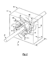
FIG. 2 is an isometric view of current sensor traces of an orthogonal radio frequency (RF) current and voltage sensor according to various embodiments of the present disclosure; -
FIGS. 3(a)-(c) are plan views of the current sensor traces ofFIG. 2 ; -
FIG. 4 is a plan view of current sensor traces of an orthogonal radio frequency (RF) current and voltage sensor according to various embodiments of the present disclosure; -
FIG. 5(a) is schematic diagram of a current sensor of the prior art; -
FIGS. 5(b)-(c) and6 are schematic diagrams of a current sensor according to various embodiments of the present disclosure; -
FIG. 7 is a circuit diagram of a circuit that represents the capacitive coupling relationship between the voltage at points A and B to that of the conductor in the current sensor ofFIG. 6 ; -
FIG. 8 is a schematic diagram of a voltage current sensor according to various embodiments of the present disclosure; and -
FIGS. 9(a)-(b) are plan views of circular conductive rings of a voltage current sensor according to various embodiments of the present disclosure. - A radio frequency (RF) current sensor, which is also known as a probe, generates a signal that represents the magnitude of current flow through an RF conductor. The current probe can be combined with a voltage probe to form an RF voltage/current (VI) probe that generates a second signal that represents the RF voltage with respect to a reference potential, such as an RF ground or shield conductor.
- RF current and VI probes are used in RF control circuits to provide feedback information. The feedback information may be used to control an RF amplifier that provides the RF power that is being measured. In some applications the RF power is employed to generate plasma for semiconductor manufacturing, metal coating, or micromachining processes. While operating at certain frequencies, for example low frequencies or high frequencies, the VI probe may experience interference due to parasitic resonance within the components of the VI probe. Additionally, the low frequency coupling of the sensor to the center conductor may be low. Accordingly, the principles of the present disclosure may be arranged to improve VI probe frequency responses.
- Referring now to
FIG. 1 , an orthogonal radio frequency (RF) voltage/current (VI)probe 10 is shown.VI probe 10 includes a printed circuit board (PCB) 12 with at least four conductive layers. Afirst exterior layer 14a and asecond exterior layer 14b are parallel with each other and maintained in spaced relationship by an insulating substrate of thePCB 12. First andsecond layers vias 16 electrically connect ground planes 14 to each other.Vias 16 can be radially spaced around a perimeter of anaperture 18.Vias 16 are electrically insulated from the inner layers of thePCB 12, which are described below. Ground planes 14 and vias 16 connect to an outer layer of a coaxial cable (not shown) that carries the RF current being measured. A center conductor of the coaxial cable connects to aconductor 20 that is axially and concentrically positioned withinaperture 18.VI probe 10 may also include a plurality of mountingholes 13 to assist in coupling theVI probe 10 to the RF power generator (not shown) to be controlled. - A second plurality of
vias 22 are electrically insulated from ground planes 14 and connect current loop-back traces that are located on inner layers of thePCB 12. A third plurality ofvias 24 are also electrically insulated from ground planes 14 and implement part of a voltage sensor H field cancellation structure.Vias PCB 12 are described below in more detail.
ThePCB 12 may also include an embeddedcore ring 42. Thecore ring 42 is embedded in at least one layer of thePCB 12. Further, thecore ring 42 is arranged between the vias 22 and 24 andcurrent sensor pads 30. Thecore ring 42 is arranged to increase a magnetic flux of theVI probe 10. - The
core ring 42 comprises material that increases a permeability of a medium in a magnetic field of theVI probe 10. For example, the medium in the magnetic field may be comprised of air and thecore ring 42 comprises material with a higher permeability than air. For example only, thecore ring 42 may comprise a ferromagnetic material or a ferrimagnetic material. By embedding thecore ring 42 in thePCB 12 between the vias 22 and 24 and thecurrent sensor pads 30, the permeability of the medium (i.e., thecore ring 42 material) is increased in the magnetic field. As the permeability of the medium in the magnetic field increases, the related magnetic flux increases. The dynamic range of theVI probe 10 may be controlled by selectively adjusting the magnetic flux. In order to reduce stress on thePCB 12, thecore ring 42 may be constructed of a material with a coefficient of thermal expansion the same or less than the non-conductive material of thePCB 12. - The
PCB 12 may also include traces and pads, which are generically indicated at 28, for mounting electronic circuit components that may be connected to ground plane 14 and the various traces of the inner layers of thePCB 12. Examples of components include: connectors for providing power to the electronic circuits and/or taking electrical signals from them, amplifiers, transformers, and/or filters that buffer and/or condition the signals that represent the RF voltage and/or current ofconductor 20, and the like. - Referring now to
FIGS. 2-3 , various views of thePCB 12 are shown. Ground planes 14, vias 16 and vias 24 are omitted for clarity. A firstinner layer 32 includestraces substrate 36. A secondinner layer 34 includesmore traces substrate 36.Traces substrate 36 may contain one or more additional conductive layers that are not shown. The additional conductive layers may, e.g., implement a voltage sensor that is described below. - First and second
inner layers Vias 22 extend between and connect associated traces 44 on the first and second inner layers as is described below. Associated traces 44 are also connected by respectivecurrent sensor pads 30 that are formed along walls ofaperture 18.Current sensor pads 30 can be plated to the edge ofaperture 18 insubstrate 36 and cut to shape by laser, mechanical abrasion or other manufacturing technique. -
Insulator substrate 36 gives current sensor pads 30 a length L. While RF current flows throughconductor 20, a magnetic field rotates aroundconductor 20. The magnetic field can be defined by Biot-Savart Law, which provides
where radius is the distance betweenconductor 20 andcurrent sensor pads 30, ACcurrent is the current flowing throughconductor 20, and µ0 is the magnetic constant, equal to 4π×10-7 H / m. The magnetic field crossescurrent sensor pads 30. - From Faraday's law, the induced voltage is a function of the length L of
current sensor pads 30, a rate of change of the magnetic field, and a height of a loop formed bycurrent sensor pads 30, traces 44, andvias 22. Increasing the length L, such as by increasing a thickness ofsubstrate 36, increases coupling between the RF coaxial cable (not shown) andVI probe 10. - As L increases, the diameter of
vias 22 may also need to be increased in order to reduce the risk of breaking drills duringPCB 36 fabrication. Increasing the diameter ofvias 22 also increases the size of the sensor and/or reduces the number ofcurrent sensor pads 30 or loops (described below) that fit along the perimeter ofaperture 18. Increasing the diameter ofvias 22 also yields a proportional increase to the capacitive coupling toconductor 20, which allows the electric field ("E field") produced byconductor 20 to contaminate the desired current signals and reduce the dynamic range of theVI probe 10. In various embodiments, the width of thecurrent sensor pads 30 may be made as narrow as is practicable to mitigate E field contamination and dynamic range issues. Edge platedcurrent sensor pads 30 reduce the size and number ofvias 22 required to makeVI probe 10, which reduces E field contamination of the current signal. The current signal represents the current flowing throughconductor 20 and is taken from traces 44. - In another embodiment, the dynamic range of the
VI probe 10 is increased by increasing thecurrent sensor pad 30 length (L). In order to increase the length of thecurrent sensor pads 30, asecond PCB 15 may be coupled to thePCB 12 as shown inFIG. 2 . Thesecond PCB 15 may be coupled to thePCB 12 with a coupling layer (not show) between thesecond PCB 15 and thePCB 12. The coupling layer consists of a conductive material arranged to electrically bind thesecond PCB 15 to thePCB 12. For example, the coupling layer may consist of copper. In some embodiments, thecurrent sensor pads 30 may be connected in series from the second PCB15 to thePCB 12. In yet another embodiment, thecurrent sensor pads 30 may be connected in parallel from thesecond PCB 15 and thePCB 12. While only asecond PCB 15 is shown coupled to thePCB 12, it is understood that any number of PCBs may be coupled to thePCB 12, for example, a third, fourth, or fifth PCB. - In another embodiment, the dynamic range of the
VI probe 10 may be increased by embedding thecore ring 42 into thesecond PCB 15 and thePCB 12. Thecore ring 42 may be embedded between the vias 22 and 24, thecurrent sensor pads 30, and traces 44 on thesecond PCB 15 and thePCB 12 respectively. Thecore ring 42 is arranged to increase a magnetic flux of theVI probe 10. For example, thecore ring 42 is made of a material that increases the permeability of the medium in a magnetic field of theVI probe 10. As the permeability of the medium in the magnetic field increases, the related magnetic flux increases. WhileFIG. 2 shows thecore ring 42 embedded on both thesecond PCB 15 and thePCB 12, it is understood that thecore ring 42 may be embedded in either, both, or neither of thesecond PCB 15 and thePCB 12. - The dynamic range of the
VI probe 10 may be further increased by selectively adjusting the parameters of thevias current sensor pads 30, and the traces 44. For example, thecore ring 42 is encircled by a plurality of windings. The plurality of windings is constructed of thevias current sensor pads 30, and the traces 44. The resonance of theVI probe 10 can be controlled by selectively adjusting the number of windings and/or selectively adjusting the size of thevias current sensor pads 30, and the traces 44. By controlling the resonance of theVI probe 10, the dynamic range of theVI probe 10 may be increased. - Traces 44 are shown in more detail in
FIGS. 3(a)-3(c) .Traces 44a and traces 44b are connected to form two entwined loops of wire.Traces FIG. 3(a) connect thecurrent sensor pads 30 to the loop back vias 22. The loop back vias 22 connect to the backside of the sensor to anothertrace current sensor pad 30, as shown inFIG. 3(c) . For ease of understanding,FIG. 3 depicts the two loops astraces hexagon 40 ofFIG. 3 may be a common ground point for both loops as one of the RFpath ground vias 16. This common ground system may be used to reduce ground loops. - By alternating the
current sensor pads 30 with spatial uniformity along the inner perimeter of theopening 18, the current loops provide an autocorrecting feature from movement of theconductor 20, such as from assembly/disassembly ofVI probe 10 or thermal changes in theVI probe 10 during operation. The autocorrecting feature of the design works by maintaining a constant sum total distance from theconductor 20 to thecurrent sensor pads 30. If, for example, theconductor 20 moves to the right, the rightcurrent sensor pad 30 toconductor 20 distance decreases, but the leftcurrent sensor pad 30 to centerconductor 20 increases by the same amount, keeping the sum total distance and current signal level the same. - Another view of the
PCB 12 according to various embodiments of the present disclosure is shown inFIG. 4 . Ground planes 14 and vias 16 are omitted for clarity. A firstinner layer 32 includestraces substrate 36. A secondinner layer 34 includesmore traces substrate 36.Traces substrate 36 may contain one or more additional conductive layers that are not shown. The additional conductive layers may, e.g., implement a voltage sensor that is described below. In thePCB 12 illustrated inFIG. 4 , vias 24 are electrically connected tocurrent sensor pads 30 to implement a voltage sensor in the manner described below (see, for example,FIG. 8 ). - A schematic representation of a prior art current sensor is illustrated in
FIG. 5(a) . From Ampere's law, with the RF current traveling into the page, a magnetic field will be generated in a clockwise direction around theconductor 20. The magnetic field will induce a current on thepickup loops 60 to flow through thetransformer 50. Any electric fields picked up by theloops 60 will be shorted to ground. The circuit ofFIG. 5(a) may act as a current sensor with thesensor loops 60 placed end to end (in series) such that there is no coupling between theloops 60. - A schematic representation of a current sensor according to various embodiments of the present disclosure is illustrated in
FIG. 5(b) . In the circuit ofFIG. 5(b) , a common ground is utilized for theloops 60. From Ampere's law, with the RF current traveling into the page, a magnetic field will be generated in a clockwise direction around theconductor 20. The magnetic field will induce a current on thepickup loops 60 to flow through thetransformer 50. Any electric fields picked up by theloops 60 will be shorted to ground. The circuit ofFIG. 5(b) includes twoloops 60 next to each other (or parallel to each other) and there is no coupling between theloops 60. - A schematic representation of a current sensor according to various embodiments of the present disclosure is illustrated in
FIG. 5(c) . In the circuit ofFIG. 5(c) , theloops 60 are not connected to a common ground. From Ampere's law, with the RF current traveling into the page, a magnetic field will be generated in a clockwise direction around theconductor 20. Aresistor 55 in series with each of the two current pick uploops 60 may be included. Theresistors 55 may be used to match the sensor impedance to any accompanying processing unit that may be utilized with theVI probe 10, which will result in lower reflected signals, lower noise and maximum sensor signal power transfer to the processing unit. The magnetic field will induce a current on thepickup loops 60 to flow through thetransformer 50 andresistors 55. The electric field picked up byloops 60 will not be shorted to ground, as in the case ofFIGS. 5(a) and 5(b) . The E fields at points A and B on thetransformer 50, however, will be equal, resulting in no current flow through thetransformer 50 due to the E field. Therefore, the E field will be effectively canceled on the secondary oroutput side 57 of thetransformer 50. Furthermore, points A and B oftransformer 50 will be at relatively the same electrical potential, which will correspond to the electrical potential of theconductor 20 plus an additional component due to contamination from the current signals generated onloops 60 by the magnetic field. - By placing the loops next to each other as depicted in
FIGS. 5(b) and 5(c) , the twocurrent loops 60 will be exposed to the same magnetic and electric fields, which results in better cancellation of the E fields and an increase in the current sensor dynamic range. The length of the current sensor pick up lines (for example, current sensor pads 30) is related to the frequency response and coupling of thesensor 10. A longer current sensor pick up will improve signal coupling and the low frequency response ofsensor 10, without decreasing the voltage breakdown of theVI probe 10 and other adverse effects. - The
transformer 50 generally has a turn ratio ("N") with respect to the primary and secondary windings. Theresistors 55 compensate for the real portion of the output impedance. The imaginary portion of the output impedance may be compensated for by presenting real transmission line sensor sections or matching/filter circuits. In various embodiments, the values of theresistors 55 may be defined by:
where Zoutput is the desired output impedance presented to the analysis unit and N is the transformer turns ratio. - Referring now to
FIG. 6 , a schematic representation of yet another current sensor according to various embodiments of the present disclosure is illustrated. In the circuit ofFIG. 6 , the circuit ofFIG. 5(c) is modified by removing the ground and connecting the loops 60 (for example, end-to-end) to form onecontinuous loop 60. This may be accomplished, for example, by connecting thetraces FIGS. 3(a)-3(c) ) by a via at the position of thehexagon 40. In this arrangement, the electric field impinged on the current sensor is not shorted to ground and, therefore, the E field potential will cause current to flow through theseries resistors 55. The current from the E field will aid in one current loop while reduce the current in the other current loop, which may result in a portion of the E field signal to pass through thetransformer 50. This E field contamination may reduce the dynamic range of the current sensor. By removing the current sensor ground from the RF ground, the current sensor ground will not be affected by the RF currents flowing through thePCB board 12 and the current sensor will only measure the current of theconductor 20. - From Ampere's law, with the RF current traveling into the page, a magnetic field will be generated in a clockwise direction around the
conductor 20. Theresistors 55 may be used to match the sensor impedance to any accompanying processing unit that may be utilized with theVI probe 10, which will result in lower reflected signals, lower noise and maximum sensor signal power transfer to the processing unit. The magnetic field will induce a current on thepickup loops 60 to flow through thetransformer 50 andresistors 55. As discussed above, the electric field picked up byloops 60 will not be shorted to ground, as in the case ofFIGS. 5(a) and 5(b) . The E fields at points A and B on thetransformer 50, however, will be equal, resulting in no current flow through thetransformer 50 due to the E field. Therefore, the E field will be effectively canceled on the secondary oroutput side 57 of thetransformer 50. Furthermore, points A and B oftransformer 50 will be at relatively the same electrical potential. - As described above, the voltage potential at points A and B are proportional to the electric potential in the
conductor 20, due to capacitive coupling. The voltage potential at points A and B can be thought of as the electrical potential of theconductor 20 plus an additional component due to contamination from the current signals generated onloops 60 by the magnetic field. -
FIG. 7 is a circuit diagram that represents a circuit showing a capacitive coupling relationship between the voltage at points A and B to that of the voltage of theconductor 20 ofFIG. 6 . InFIG. 7 , the resistor Rm is the measurement input impedance, such as in an analog-to-digital converter or receiver; Im represents the current produced by the changing magnetic field around theconductor 20; Cc represents the distributed coupling capacitance between theconductor 20 and thecurrent loops 60; and Ve is the RF voltage of theconductor 20. - Utilizing the arrangement of
FIG. 7 , the RF voltage potential ofconductor 20 may be defined by Guass's law. Using nodal equations to determine the voltage at points A and B (VA and VB, respectively) and letting:

and
- Kirchhoffs current law equations for each node yields:


- If we collect like terms:


- Solving for VA and VB yields:
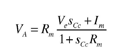

- Adding VA and VB signals (Vsum = VA + VB) with a center tap of the transformer 50 (or, alternatively, by an analog-to-digital converter/digital signal processing ("ADC/DSP") system) yields:


- The result is the E Field of
conductor 20, Ve, and an attenuation term. Subtracting VB from VA (Vdiff = VA - VB) with a transformer 50 (secondary winding) or ADC/DSP system yields:
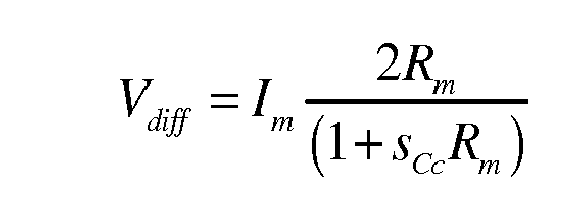
- The result is current flowing through
conductor 20, Im, and an attenuation term. From these equations, the voltage (Ve) and current (Im) ofconductor 20 may be determined. - A schematic representation of a voltage/current sensor according to various embodiments of the present disclosure is illustrated in
FIG. 8 . From Ampere's law, with the RF current traveling into the page, a magnetic field will be generated in a clockwise direction around theconductor 20. The magnetic field will induce a current on thepickup loops 60 to flow through thetransformer 50. Similar to the circuit illustrated inFIG. 6 , the electric field impinged on the voltage/current sensor is not shorted to ground and, therefore, the E field potential will cause current to flow through theseries resistors 55. The current from the E field will aid in one current loop while reduce the current in the other current loop, which may result in a portion of the E field signal to pass through thetransformer 50. This E field contamination may reduce the dynamic range of the current sensor.
By removing the current sensor ground from the RF ground, the current sensor ground will not be affected by the RF currents flowing through thePCB board 12 and the current sensor will only measure the current of theconductor 20. The electrical signal representing the current of theconductor 20 may be obtained from thesecondary side 57 of thetransformer 50. A center tap 59 of thetransformer 50 may be utilized to obtain the electrical signal representing the voltage of theconductor 20. From these electrical signals, the voltage and current of theconductor 20 may be determined, e.g., based on the equations set forth above. - Referring now to
FIGS. 9(a) and 9(b) , various views of thePCB 12 are shown. Ground planes 14, vias 16 and vias 22 are omitted for clarity. A thirdinner layer 33 includes a circularconductive ring 102a that is formed on insulatingsubstrate 36. A fourthinner layer 35 includes another circularconductive ring 102b on the opposite side ofsubstrate 36. Circularconductive rings vias 24. Each of the circular conductive rings 102 defines a plane that is orthogonal to the longitudinal axis of theconductor 20. Furthermore, traces 104 couple each of the circular conductive rings 102 tovoltage sensor pads 100 that are formed along walls ofaperture 18. - In some embodiments, the
voltage sensor pads 100 may be the same as thecurrent sensor pads 30 described above.Voltage sensor pads 100 can be plated to the edge ofaperture 18 insubstrate 36 and cut to shape by laser, mechanical abrasion or other manufacturing technique.Hexagon 40 may be utilized as a reference ground for determining a voltage of theconductor 20. Theinner layer 33 also includes an embeddedcore ring 42. Thecore ring 42 is embedded in theinner layer 33 between circularconductive rings - The foregoing description is merely illustrative in nature and is in no way intended to limit the disclosure, its application, or uses. The broad teachings of the disclosure can be implemented in a variety of forms. Therefore, while this disclosure includes particular examples, the true scope of the disclosure should not be so limited since other modifications will become apparent upon a study of the drawings, the specification, and the following claims. For purposes of clarity, the same reference numbers will be used in the drawings to identify similar elements. As used herein, the phrase at least one of A, B, and C should be construed to mean a logical (A or B or C), using a non-exclusive logical OR. It should be understood that one or more steps within a method may be executed in different order (or concurrently) without altering the principles of the present disclosure.
- It will be understood that the invention has been described above purely by way of example, and modifications of detail can be made within the scope of the invention.
- Each feature disclosed in the description, and (where appropriate) the claims and drawings may be provided independently or in any appropriate combination.
- Any reference numerals appearing in the claims are by way of illustration only and shall have no limiting effect on the scope of the claims.
Claims (14)
- A radio frequency (RF) sensor system comprising:a printed circuit board (PCB) including a first exterior layer, a second exterior layer, a first interior layer, a second interior layer, and an inner perimeter that defines an aperture through the PCB;a first loop comprising a first plurality of sensor pads coupled to a first plurality of vias by a first plurality of traces, the first plurality of sensor pads being arranged on the inner perimeter;a second loop comprising a second plurality of sensor pads coupled to a second plurality of vias by a second plurality of traces, the second plurality of sensor pads being arranged on the inner perimeter; anda core ring embedded within the first interior layer proximal to the first plurality of sensor pads, the first plurality of vias, and the first plurality of traces;wherein a center conductor for carrying RF current extends through the aperture and the first and second loops generate an electrical signal based on the first and second plurality of sensor pads, the first and second plurality of vias, the first and second plurality of traces, and the core ring.
- The RF sensor system of claim 1 wherein the core ring consists of a medium with a greater permeability than air.
- The RF sensor system of claim 1 or 2, wherein the core ring consists of a ferromagnetic material.
- The RF sensor system of any preceding claim, wherein the core ring has a coefficient of thermal expansion equal to the coefficient of expansion of the first and second exterior layers and the first and second interior layers.
- The RF sensor system of any of claims 1 to 3, wherein the core ring has a coefficient of thermal expansion of less than the coefficient of expansion of the first and second exterior layers and the first and second interior layers.
- The RF sensor system of any preceding claim, wherein at least one of a plurality of characteristics of the plurality of vias is selectively adjusted based on a resonance of the RF sensor.
- The RF sensor system of any preceding claim, further comprising a second PCB including a third exterior layer, a fourth exterior layer, a third interior layer, a fourth interior layer, and an second inner perimeter that defines a second aperture through the second PCB;
a third loop comprising a third plurality of sensor pads coupled to a third plurality of vias by a third plurality of traces, the third plurality of sensor pads being arranged on the second inner perimeter; and
a fourth loop comprising a fourth plurality of sensor pads coupled to a fourth plurality of vias by a fourth plurality of traces, the fourth plurality of sensor pads being arranged on the second inner perimeter;
preferably, wherein the fourth exterior layer is electrically bound to the first exterior layer;
more preferably, wherein the first plurality of sensor pads, the second plurality of sensor pads, third plurality of sensor pads, and the fourth plurality of sensor pads are electronically connected in series or in parallel. - A radio frequency (RF) sensing method comprising:defining an aperture through a printed circuit board (PCB), wherein the PCB includes a first exterior layer, a second exterior layer, a first interior layer, a second interior layer, and an inner perimeter;coupling a first loop comprising a first plurality of sensor pads to a first plurality of vias by a first plurality of traces, arranging the first plurality of sensor pads on the inner perimeter;coupling a second loop comprising a second plurality of sensor pads to a second plurality of vias by a second plurality of traces, arranging the second plurality of sensor pads on the inner perimeter; andembedding a core ring within the first interior layer proximal to the first plurality of sensor pads, the first plurality of vias, and the first plurality of traces;wherein a center conductor for carrying RF current extends through the aperture and the first and second loops generate an electrical signal based on the first and second plurality of sensor pads, the first and second plurality of vias, the first and second plurality of traces, and the core ring.
- The RF sensing method of claim 8 wherein the core ring consists of a medium with a greater permeability than air.
- The RF sensing method of claim 8 or 9, wherein the core ring consists of a ferromagnetic material.
- The RF sensing method of any of claims 8 to 10, wherein the core ring has a coefficient of thermal expansion equal to the coefficient of expansion of the first and second exterior layers and the first and second interior layers.
- The RF sensing method of any of claims 8 to 10, wherein the core ring has a coefficient of thermal expansion of less than the coefficient of expansion of the first and second exterior layers and the first and second interior layers.
- The RF sensing method of any of claims 8 to 12, wherein at least one of a plurality of characteristics of the plurality of vias is selectively adjusted based on a resonance of the RF sensor.
- The RF sensing method of claims 8 to 13, further comprising defining a second aperture a second PCB, wherein the second PCB includes a third exterior layer, a fourth exterior layer, a third interior layer, a fourth interior layer, and a second inner perimeter;
coupling a third loop comprising a third plurality of sensor pads to a third plurality of vias by a third plurality of traces, the third plurality of sensor pads being arranged on the second inner perimeter; and
coupling a fourth loop comprising a fourth plurality of sensor pads to a fourth plurality of vias by a fourth plurality of traces, the fourth plurality of sensor pads being arranged on the second inner perimeter;
preferably, further comprising electrically binding the fourth exterior layer to the first exterior layer;
more preferably, further comprising electrically connecting the first plurality of sensor pads, the second plurality of sensor pads, third plurality of sensor pads, and the fourth plurality of sensor pads in series or in parallel.
Applications Claiming Priority (2)
| Application Number | Priority Date | Filing Date | Title |
|---|---|---|---|
| US201261684013P | 2012-08-16 | 2012-08-16 | |
| US13/828,628 US9291649B2 (en) | 2012-08-16 | 2013-03-14 | On the enhancements of planar based RF sensor technology |
Publications (2)
| Publication Number | Publication Date |
|---|---|
| EP2699064A2 true EP2699064A2 (en) | 2014-02-19 |
| EP2699064A3 EP2699064A3 (en) | 2017-12-06 |
Family
ID=49035311
Family Applications (1)
| Application Number | Title | Priority Date | Filing Date |
|---|---|---|---|
| EP13180591.3A Withdrawn EP2699064A3 (en) | 2012-08-16 | 2013-08-15 | Planar based RF sensor technology |
Country Status (7)
| Country | Link |
|---|---|
| US (1) | US9291649B2 (en) |
| EP (1) | EP2699064A3 (en) |
| JP (3) | JP6069129B2 (en) |
| KR (1) | KR101787420B1 (en) |
| CN (1) | CN103592494B (en) |
| SG (1) | SG2013060918A (en) |
| TW (1) | TWI499783B (en) |
Families Citing this family (50)
| Publication number | Priority date | Publication date | Assignee | Title |
|---|---|---|---|---|
| US10431428B2 (en) | 2014-01-10 | 2019-10-01 | Reno Technologies, Inc. | System for providing variable capacitance |
| US10455729B2 (en) | 2014-01-10 | 2019-10-22 | Reno Technologies, Inc. | Enclosure cooling system |
| US9844127B2 (en) | 2014-01-10 | 2017-12-12 | Reno Technologies, Inc. | High voltage switching circuit |
| US9755641B1 (en) | 2014-01-10 | 2017-09-05 | Reno Technologies, Inc. | High speed high voltage switching circuit |
| US9697991B2 (en) | 2014-01-10 | 2017-07-04 | Reno Technologies, Inc. | RF impedance matching network |
| US9196459B2 (en) | 2014-01-10 | 2015-11-24 | Reno Technologies, Inc. | RF impedance matching network |
| US9865432B1 (en) | 2014-01-10 | 2018-01-09 | Reno Technologies, Inc. | RF impedance matching network |
| US9496122B1 (en) | 2014-01-10 | 2016-11-15 | Reno Technologies, Inc. | Electronically variable capacitor and RF matching network incorporating same |
| KR101632603B1 (en) * | 2014-09-30 | 2016-06-24 | 세메스 주식회사 | Current sensor and plasma processing apparatus |
| US9958480B2 (en) | 2015-02-10 | 2018-05-01 | Qualcomm Incorporated | Apparatus and method for a current sensor |
| US11017983B2 (en) | 2015-02-18 | 2021-05-25 | Reno Technologies, Inc. | RF power amplifier |
| US12119206B2 (en) | 2015-02-18 | 2024-10-15 | Asm America, Inc. | Switching circuit |
| US10340879B2 (en) | 2015-02-18 | 2019-07-02 | Reno Technologies, Inc. | Switching circuit |
| US9729122B2 (en) | 2015-02-18 | 2017-08-08 | Reno Technologies, Inc. | Switching circuit |
| US9306533B1 (en) | 2015-02-20 | 2016-04-05 | Reno Technologies, Inc. | RF impedance matching network |
| US9525412B2 (en) | 2015-02-18 | 2016-12-20 | Reno Technologies, Inc. | Switching circuit |
| US11342161B2 (en) | 2015-06-29 | 2022-05-24 | Reno Technologies, Inc. | Switching circuit with voltage bias |
| US11335540B2 (en) | 2015-06-29 | 2022-05-17 | Reno Technologies, Inc. | Impedance matching network and method |
| US11342160B2 (en) | 2015-06-29 | 2022-05-24 | Reno Technologies, Inc. | Filter for impedance matching |
| US10692699B2 (en) | 2015-06-29 | 2020-06-23 | Reno Technologies, Inc. | Impedance matching with restricted capacitor switching |
| US11081316B2 (en) | 2015-06-29 | 2021-08-03 | Reno Technologies, Inc. | Impedance matching network and method |
| US11150283B2 (en) | 2015-06-29 | 2021-10-19 | Reno Technologies, Inc. | Amplitude and phase detection circuit |
| US10984986B2 (en) | 2015-06-29 | 2021-04-20 | Reno Technologies, Inc. | Impedance matching network and method |
| JP6434456B2 (en) * | 2016-06-23 | 2018-12-05 | 横河電機株式会社 | Isolated voltage probe |
| JP7108623B2 (en) * | 2017-02-16 | 2022-07-28 | アプライド マテリアルズ インコーポレイテッド | Voltage-current probe for measuring high frequency power in high temperature environments and method for calibrating voltage-current probe |
| US10714314B1 (en) | 2017-07-10 | 2020-07-14 | Reno Technologies, Inc. | Impedance matching network and method |
| US11521833B2 (en) | 2017-07-10 | 2022-12-06 | Reno Technologies, Inc. | Combined RF generator and RF solid-state matching network |
| US11476091B2 (en) | 2017-07-10 | 2022-10-18 | Reno Technologies, Inc. | Impedance matching network for diagnosing plasma chamber |
| US10727029B2 (en) | 2017-07-10 | 2020-07-28 | Reno Technologies, Inc | Impedance matching using independent capacitance and frequency control |
| US11101110B2 (en) | 2017-07-10 | 2021-08-24 | Reno Technologies, Inc. | Impedance matching network and method |
| US11315758B2 (en) | 2017-07-10 | 2022-04-26 | Reno Technologies, Inc. | Impedance matching using electronically variable capacitance and frequency considerations |
| US11393659B2 (en) | 2017-07-10 | 2022-07-19 | Reno Technologies, Inc. | Impedance matching network and method |
| US11289307B2 (en) | 2017-07-10 | 2022-03-29 | Reno Technologies, Inc. | Impedance matching network and method |
| US12272522B2 (en) | 2017-07-10 | 2025-04-08 | Asm America, Inc. | Resonant filter for solid state RF impedance matching network |
| US10483090B2 (en) | 2017-07-10 | 2019-11-19 | Reno Technologies, Inc. | Restricted capacitor switching |
| US11114280B2 (en) | 2017-07-10 | 2021-09-07 | Reno Technologies, Inc. | Impedance matching with multi-level power setpoint |
| US12334307B2 (en) | 2017-07-10 | 2025-06-17 | Asm Ip Holding B.V. | Power control for rf impedance matching network |
| US11398370B2 (en) | 2017-07-10 | 2022-07-26 | Reno Technologies, Inc. | Semiconductor manufacturing using artificial intelligence |
| KR102509641B1 (en) * | 2018-08-28 | 2023-03-16 | 삼성전자주식회사 | Device for sensing radio frequency in plasma chamber and plasma chamber comprising the device |
| WO2020226963A1 (en) * | 2019-05-07 | 2020-11-12 | Lam Research Corporation | Voltage and current probe |
| US11521831B2 (en) | 2019-05-21 | 2022-12-06 | Reno Technologies, Inc. | Impedance matching network and method with reduced memory requirements |
| FR3097054B1 (en) * | 2019-06-07 | 2021-07-02 | Schneider Electric Ind Sas | Current sensor and measuring system comprising such a current sensor |
| US12546802B2 (en) * | 2021-09-29 | 2026-02-10 | Lam Research Corporation | Voltage and current probe assemblies for radio frequency current carrying conductors |
| US12224164B2 (en) | 2021-10-29 | 2025-02-11 | Tokyo Electron Limited | Radio frequency (RF) system with embedded RF signal pickups |
| KR102660899B1 (en) | 2021-11-19 | 2024-04-25 | 주식회사 뉴파워 프라즈마 | Module type sensor for detecting voltage and current of radio frequency signal onto pcb transmission line |
| KR102844445B1 (en) | 2023-06-21 | 2025-08-11 | 주식회사 뉴파워 프라즈마 | Radio frequency voltage current sensor |
| KR102854195B1 (en) | 2023-08-11 | 2025-09-03 | (주)이큐글로벌 | Radio frequency voltage current sensor |
| KR102800311B1 (en) | 2023-08-11 | 2025-04-30 | (주)이큐글로벌 | Radio frequency voltage current sensor with adjustable synthetic inductance |
| KR102870151B1 (en) | 2024-01-23 | 2025-11-13 | 서울시립대학교 산학협력단 | Current sensor and method for manufacturing current sensor |
| CN118155992B (en) * | 2024-03-20 | 2025-10-03 | 深圳供电局有限公司 | Coil module for transformer and transformer |
Family Cites Families (41)
| Publication number | Priority date | Publication date | Assignee | Title |
|---|---|---|---|---|
| US3667040A (en) * | 1970-09-28 | 1972-05-30 | Us Army | Sensor for detecting radio frequency currents in carbon bridge detonator |
| DE3817500C1 (en) | 1988-05-21 | 1989-10-05 | Rohde & Schwarz Gmbh & Co Kg, 8000 Muenchen, De | |
| US5041791A (en) * | 1989-08-07 | 1991-08-20 | Washington University | Magnetic resonance RF probe with electromagnetically isolated transmitter and receiver coils |
| JPH06216307A (en) | 1993-01-13 | 1994-08-05 | Mitsubishi Electric Corp | Resin-sealed semiconductor device |
| US5467013A (en) * | 1993-12-07 | 1995-11-14 | Sematech, Inc. | Radio frequency monitor for semiconductor process control |
| US5633648A (en) * | 1995-07-28 | 1997-05-27 | Fischer Custom Communications, Inc. | RF current-sensing coupled antenna device |
| US5834931A (en) * | 1996-10-31 | 1998-11-10 | Sematech, Inc. | RF current sensor |
| US5808415A (en) * | 1997-03-19 | 1998-09-15 | Scientific Systems Research Limited | Apparatus for sensing RF current delivered to a plasma with two inductive loops |
| JPH1183907A (en) * | 1997-09-03 | 1999-03-26 | Mitsubishi Electric Corp | How to measure high frequency current |
| JPH11101824A (en) * | 1997-09-26 | 1999-04-13 | Shimadzu Corp | Current sensor |
| JP2000228323A (en) * | 1999-02-05 | 2000-08-15 | Toshiba Corp | Rogowski coil |
| EP1183543B1 (en) * | 1999-05-25 | 2003-04-23 | Arbeitsgemeinschaft Prof. Hugel AGPH | Electrical current sensor |
| JP3945087B2 (en) * | 1999-09-29 | 2007-07-18 | 三菱電機株式会社 | Rogowski coil |
| US6501285B1 (en) * | 2000-06-20 | 2002-12-31 | Scientific Systems Research Limited | RF current sensor |
| JP2002228323A (en) * | 2001-01-26 | 2002-08-14 | Fuji Electric Co Ltd | Insulated box and box holder for delivery |
| JP2003130894A (en) * | 2001-10-29 | 2003-05-08 | Toshiba Corp | Current transformer |
| US6608446B1 (en) * | 2002-02-25 | 2003-08-19 | Eni Technology, Inc. | Method and apparatus for radio frequency (RF) metrology |
| US6661324B1 (en) * | 2002-08-01 | 2003-12-09 | Advanced Energy Industries, Inc. | Voltage and current sensor |
| JP2004119926A (en) * | 2002-09-30 | 2004-04-15 | Toshiba Corp | Current transformer and current transformer system |
| JP4103713B2 (en) * | 2003-07-18 | 2008-06-18 | 株式会社デンソー | Current detector |
| US6902646B2 (en) * | 2003-08-14 | 2005-06-07 | Advanced Energy Industries, Inc. | Sensor array for measuring plasma characteristics in plasma processing environments |
| JP2005101244A (en) * | 2003-09-25 | 2005-04-14 | Hitachi Ltd | Printed circuit board type transformer |
| US7196607B2 (en) * | 2004-03-26 | 2007-03-27 | Harris Corporation | Embedded toroidal transformers in ceramic substrates |
| EP1836716A4 (en) * | 2005-01-11 | 2009-12-23 | Innovation Engineering Llc | Method of detecting rf power delivered to a load and complex impedance of the load |
| WO2007027985A2 (en) * | 2005-09-01 | 2007-03-08 | Barth Jon E | Pulse current sensor |
| US20070166730A1 (en) * | 2006-01-19 | 2007-07-19 | Menon & Associates, Inc. | Magnetic resonance system and method to detect and confirm analytes |
| JP4916807B2 (en) | 2006-01-30 | 2012-04-18 | 株式会社ダイヘン | Voltage detection printed circuit board and voltage detector using the same |
| US7538562B2 (en) | 2006-03-20 | 2009-05-26 | Inficon, Inc. | High performance miniature RF sensor for use in microelectronics plasma processing tools |
| JP4916821B2 (en) | 2006-03-31 | 2012-04-18 | 株式会社ダイヘン | Voltage detection printed circuit board and voltage detector using the same |
| EP1884787A1 (en) * | 2006-07-10 | 2008-02-06 | S. THIIM ApS | A current sensor for measuring electric current in a conductor and a short circuit indicator system comprising such a sensor |
| US20100134286A1 (en) * | 2008-12-01 | 2010-06-03 | General Electric Company | Radio frequency based sensors employing analyte recognition element |
| JP2008134118A (en) * | 2006-11-28 | 2008-06-12 | Daihen Corp | Printed circuit board for current detection |
| US9232618B2 (en) * | 2007-08-06 | 2016-01-05 | Immunolight, Llc | Up and down conversion systems for production of emitted light from various energy sources including radio frequency, microwave energy and magnetic induction sources for upconversion |
| JP5069978B2 (en) * | 2007-08-31 | 2012-11-07 | 株式会社ダイヘン | Printed circuit board for current / voltage detection and current / voltage detector |
| US8040141B2 (en) * | 2008-04-10 | 2011-10-18 | Mks Instruments, Inc. | Orthogonal radio frequency voltage/current sensor with high dynamic range |
| JP2010232392A (en) * | 2009-03-26 | 2010-10-14 | Panasonic Electric Works Co Ltd | Zero-phase current transformer and leakage detection device |
| JP5126154B2 (en) * | 2009-04-22 | 2013-01-23 | 株式会社日本自動車部品総合研究所 | Current sensor device |
| JP5462368B2 (en) * | 2010-09-06 | 2014-04-02 | 株式会社イー・エム・ディー | Plasma processing equipment |
| WO2012117275A2 (en) * | 2011-03-01 | 2012-09-07 | Sendyne Corp. | Current sensor |
| FR2979792B1 (en) * | 2011-09-07 | 2013-10-11 | Commissariat Energie Atomique | CURRENT SENSOR |
| US20130320997A1 (en) * | 2012-06-05 | 2013-12-05 | Aileen Hayashida Efigenio | Sensor system and antenna for use in a sensor system |
-
2013
- 2013-03-14 US US13/828,628 patent/US9291649B2/en active Active
- 2013-08-12 JP JP2013167679A patent/JP6069129B2/en not_active Expired - Fee Related
- 2013-08-13 SG SG2013060918A patent/SG2013060918A/en unknown
- 2013-08-14 KR KR1020130096833A patent/KR101787420B1/en not_active Expired - Fee Related
- 2013-08-15 EP EP13180591.3A patent/EP2699064A3/en not_active Withdrawn
- 2013-08-16 CN CN201310359090.9A patent/CN103592494B/en not_active Expired - Fee Related
- 2013-08-16 TW TW102129585A patent/TWI499783B/en not_active IP Right Cessation
-
2015
- 2015-08-21 JP JP2015163847A patent/JP2016001190A/en active Pending
-
2017
- 2017-07-28 JP JP2017146593A patent/JP6490160B2/en not_active Expired - Fee Related
Also Published As
| Publication number | Publication date |
|---|---|
| JP6490160B2 (en) | 2019-03-27 |
| TWI499783B (en) | 2015-09-11 |
| CN103592494B (en) | 2016-12-28 |
| CN103592494A (en) | 2014-02-19 |
| KR101787420B1 (en) | 2017-10-19 |
| US9291649B2 (en) | 2016-03-22 |
| KR20140023229A (en) | 2014-02-26 |
| US20140049250A1 (en) | 2014-02-20 |
| JP2014038097A (en) | 2014-02-27 |
| JP2016001190A (en) | 2016-01-07 |
| SG2013060918A (en) | 2014-03-28 |
| TW201409038A (en) | 2014-03-01 |
| EP2699064A3 (en) | 2017-12-06 |
| JP6069129B2 (en) | 2017-02-01 |
| JP2017223691A (en) | 2017-12-21 |
Similar Documents
| Publication | Publication Date | Title |
|---|---|---|
| US9291649B2 (en) | On the enhancements of planar based RF sensor technology | |
| US8040141B2 (en) | Orthogonal radio frequency voltage/current sensor with high dynamic range | |
| US10859605B2 (en) | Current sensor and a method of manufacturing a current sensor | |
| JP4842562B2 (en) | Current transformer including a combination of partial circuits with a Rogowski type winding forming a complete circuit | |
| US7579824B2 (en) | High-precision Rogowski current transformer | |
| US6624624B1 (en) | Electrical current sensor | |
| JP3638342B2 (en) | Magnetic resonance system including a double-sided RF shield | |
| US11029341B2 (en) | Low-noise, large dynamic-range sensor for measuring current | |
| JP2000147002A (en) | Current probe | |
| JPS62106379A (en) | Magnetic field measuring probe | |
| KR20250141090A (en) | Current Sensor with Core and Method of Manufacturing Thereof | |
| JP7111347B2 (en) | Magnetic field detection coil and EMI antenna | |
| EP1923709B1 (en) | Active linear current transducer | |
| US20170219667A1 (en) | Planar Standing Wave Trap for a Magnetic Resonance Tomograph | |
| JP5777258B2 (en) | High power variable inductor and filter using the same | |
| US9329207B2 (en) | Surface current probe | |
| KR102870151B1 (en) | Current sensor and method for manufacturing current sensor | |
| Dąbek et al. | High immunity wafer-level measurement of MHz current | |
| JP7840587B2 (en) | Current sensor | |
| JPH07201537A (en) | Resistor |
Legal Events
| Date | Code | Title | Description |
|---|---|---|---|
| AK | Designated contracting states |
Kind code of ref document: A2 Designated state(s): AL AT BE BG CH CY CZ DE DK EE ES FI FR GB GR HR HU IE IS IT LI LT LU LV MC MK MT NL NO PL PT RO RS SE SI SK SM TR |
|
| AX | Request for extension of the european patent |
Extension state: BA ME |
|
| PUAI | Public reference made under article 153(3) epc to a published international application that has entered the european phase |
Free format text: ORIGINAL CODE: 0009012 |
|
| PUAL | Search report despatched |
Free format text: ORIGINAL CODE: 0009013 |
|
| AK | Designated contracting states |
Kind code of ref document: A3 Designated state(s): AL AT BE BG CH CY CZ DE DK EE ES FI FR GB GR HR HU IE IS IT LI LT LU LV MC MK MT NL NO PL PT RO RS SE SI SK SM TR |
|
| AX | Request for extension of the european patent |
Extension state: BA ME |
|
| RIC1 | Information provided on ipc code assigned before grant |
Ipc: G01R 15/18 20060101ALI20171102BHEP Ipc: H01F 27/28 20060101ALI20171102BHEP Ipc: H05H 1/46 20060101AFI20171102BHEP Ipc: H01F 38/30 20060101ALN20171102BHEP |
|
| RIN1 | Information on inventor provided before grant (corrected) |
Inventor name: BROOKS, RAYMOND Inventor name: BROWN, DENNIS M. Inventor name: COUMOU, DAVID J. |
|
| STAA | Information on the status of an ep patent application or granted ep patent |
Free format text: STATUS: REQUEST FOR EXAMINATION WAS MADE |
|
| 17P | Request for examination filed |
Effective date: 20180606 |
|
| RBV | Designated contracting states (corrected) |
Designated state(s): AL AT BE BG CH CY CZ DE DK EE ES FI FR GB GR HR HU IE IS IT LI LT LU LV MC MK MT NL NO PL PT RO RS SE SI SK SM TR |
|
| STAA | Information on the status of an ep patent application or granted ep patent |
Free format text: STATUS: EXAMINATION IS IN PROGRESS |
|
| 17Q | First examination report despatched |
Effective date: 20210527 |
|
| GRAP | Despatch of communication of intention to grant a patent |
Free format text: ORIGINAL CODE: EPIDOSNIGR1 |
|
| STAA | Information on the status of an ep patent application or granted ep patent |
Free format text: STATUS: GRANT OF PATENT IS INTENDED |
|
| INTG | Intention to grant announced |
Effective date: 20240419 |
|
| STAA | Information on the status of an ep patent application or granted ep patent |
Free format text: STATUS: THE APPLICATION IS DEEMED TO BE WITHDRAWN |
|
| 18D | Application deemed to be withdrawn |
Effective date: 20240820 |