EP2698746A2 - Verfahren und System zur sicheren Konfiguration einer elektronischen Vorrichtung über ein RFID IC - Google Patents
Verfahren und System zur sicheren Konfiguration einer elektronischen Vorrichtung über ein RFID IC Download PDFInfo
- Publication number
- EP2698746A2 EP2698746A2 EP13173713.2A EP13173713A EP2698746A2 EP 2698746 A2 EP2698746 A2 EP 2698746A2 EP 13173713 A EP13173713 A EP 13173713A EP 2698746 A2 EP2698746 A2 EP 2698746A2
- Authority
- EP
- European Patent Office
- Prior art keywords
- rfid
- cpu
- electronic device
- circuit board
- communications channel
- Prior art date
- Legal status (The legal status is an assumption and is not a legal conclusion. Google has not performed a legal analysis and makes no representation as to the accuracy of the status listed.)
- Withdrawn
Links
Images




Classifications
-
- G—PHYSICS
- G06—COMPUTING OR CALCULATING; COUNTING
- G06K—GRAPHICAL DATA READING; PRESENTATION OF DATA; RECORD CARRIERS; HANDLING RECORD CARRIERS
- G06K19/00—Record carriers for use with machines and with at least a part designed to carry digital markings
- G06K19/06—Record carriers for use with machines and with at least a part designed to carry digital markings characterised by the kind of the digital marking, e.g. shape, nature, code
- G06K19/067—Record carriers with conductive marks, printed circuits or semiconductor circuit elements, e.g. credit or identity cards also with resonating or responding marks without active components
- G06K19/07—Record carriers with conductive marks, printed circuits or semiconductor circuit elements, e.g. credit or identity cards also with resonating or responding marks without active components with integrated circuit chips
- G06K19/073—Special arrangements for circuits, e.g. for protecting identification code in memory
- G06K19/07309—Means for preventing undesired reading or writing from or onto record carriers
- G06K19/07363—Means for preventing undesired reading or writing from or onto record carriers by preventing analysis of the circuit, e.g. dynamic or static power analysis or current analysis
-
- G—PHYSICS
- G06—COMPUTING OR CALCULATING; COUNTING
- G06F—ELECTRIC DIGITAL DATA PROCESSING
- G06F21/00—Security arrangements for protecting computers, components thereof, programs or data against unauthorised activity
- G06F21/50—Monitoring users, programs or devices to maintain the integrity of platforms, e.g. of processors, firmware or operating systems
- G06F21/57—Certifying or maintaining trusted computer platforms, e.g. secure boots or power-downs, version controls, system software checks, secure updates or assessing vulnerabilities
-
- G—PHYSICS
- G06—COMPUTING OR CALCULATING; COUNTING
- G06F—ELECTRIC DIGITAL DATA PROCESSING
- G06F21/00—Security arrangements for protecting computers, components thereof, programs or data against unauthorised activity
- G06F21/60—Protecting data
- G06F21/606—Protecting data by securing the transmission between two devices or processes
-
- G—PHYSICS
- G06—COMPUTING OR CALCULATING; COUNTING
- G06F—ELECTRIC DIGITAL DATA PROCESSING
- G06F21/00—Security arrangements for protecting computers, components thereof, programs or data against unauthorised activity
- G06F21/60—Protecting data
- G06F21/62—Protecting access to data via a platform, e.g. using keys or access control rules
- G06F21/629—Protecting access to data via a platform, e.g. using keys or access control rules to features or functions of an application
-
- G—PHYSICS
- G06—COMPUTING OR CALCULATING; COUNTING
- G06K—GRAPHICAL DATA READING; PRESENTATION OF DATA; RECORD CARRIERS; HANDLING RECORD CARRIERS
- G06K19/00—Record carriers for use with machines and with at least a part designed to carry digital markings
- G06K19/06—Record carriers for use with machines and with at least a part designed to carry digital markings characterised by the kind of the digital marking, e.g. shape, nature, code
- G06K19/067—Record carriers with conductive marks, printed circuits or semiconductor circuit elements, e.g. credit or identity cards also with resonating or responding marks without active components
- G06K19/07—Record carriers with conductive marks, printed circuits or semiconductor circuit elements, e.g. credit or identity cards also with resonating or responding marks without active components with integrated circuit chips
- G06K19/073—Special arrangements for circuits, e.g. for protecting identification code in memory
-
- H—ELECTRICITY
- H05—ELECTRIC TECHNIQUES NOT OTHERWISE PROVIDED FOR
- H05K—PRINTED CIRCUITS; CASINGS OR CONSTRUCTIONAL DETAILS OF ELECTRIC APPARATUS; MANUFACTURE OF ASSEMBLAGES OF ELECTRICAL COMPONENTS
- H05K1/00—Printed circuits
- H05K1/02—Details
- H05K1/0275—Security details, e.g. tampering prevention or detection
-
- H—ELECTRICITY
- H10—SEMICONDUCTOR DEVICES; ELECTRIC SOLID-STATE DEVICES NOT OTHERWISE PROVIDED FOR
- H10W—GENERIC PACKAGES, INTERCONNECTIONS, CONNECTORS OR OTHER CONSTRUCTIONAL DETAILS OF DEVICES COVERED BY CLASS H10
- H10W42/00—Arrangements for protection of devices
- H10W42/40—Arrangements for protection of devices protecting against tampering, e.g. unauthorised inspection or reverse engineering
-
- H—ELECTRICITY
- H10—SEMICONDUCTOR DEVICES; ELECTRIC SOLID-STATE DEVICES NOT OTHERWISE PROVIDED FOR
- H10W—GENERIC PACKAGES, INTERCONNECTIONS, CONNECTORS OR OTHER CONSTRUCTIONAL DETAILS OF DEVICES COVERED BY CLASS H10
- H10W90/00—Package configurations
-
- H—ELECTRICITY
- H05—ELECTRIC TECHNIQUES NOT OTHERWISE PROVIDED FOR
- H05K—PRINTED CIRCUITS; CASINGS OR CONSTRUCTIONAL DETAILS OF ELECTRIC APPARATUS; MANUFACTURE OF ASSEMBLAGES OF ELECTRICAL COMPONENTS
- H05K1/00—Printed circuits
- H05K1/16—Printed circuits incorporating printed electric components, e.g. printed resistors, capacitors or inductors
- H05K1/165—Printed circuits incorporating printed electric components, e.g. printed resistors, capacitors or inductors incorporating printed inductors
-
- H—ELECTRICITY
- H05—ELECTRIC TECHNIQUES NOT OTHERWISE PROVIDED FOR
- H05K—PRINTED CIRCUITS; CASINGS OR CONSTRUCTIONAL DETAILS OF ELECTRIC APPARATUS; MANUFACTURE OF ASSEMBLAGES OF ELECTRICAL COMPONENTS
- H05K1/00—Printed circuits
- H05K1/18—Printed circuits structurally associated with non-printed electric components
- H05K1/182—Printed circuits structurally associated with non-printed electric components associated with components mounted in printed circuit boards [PCB], e.g. insert-mounted components [IMC]
- H05K1/183—Printed circuits structurally associated with non-printed electric components associated with components mounted in printed circuit boards [PCB], e.g. insert-mounted components [IMC] associated with components mounted in and supported by recessed areas of the PCBs
-
- H—ELECTRICITY
- H05—ELECTRIC TECHNIQUES NOT OTHERWISE PROVIDED FOR
- H05K—PRINTED CIRCUITS; CASINGS OR CONSTRUCTIONAL DETAILS OF ELECTRIC APPARATUS; MANUFACTURE OF ASSEMBLAGES OF ELECTRICAL COMPONENTS
- H05K2201/00—Indexing scheme relating to printed circuits covered by H05K1/00
- H05K2201/10—Details of components or other objects attached to or integrated in a printed circuit board
- H05K2201/10007—Types of components
- H05K2201/10098—Components for radio transmission, e.g. radio frequency identification [RFID] tag, printed or non-printed antennas
-
- H—ELECTRICITY
- H10—SEMICONDUCTOR DEVICES; ELECTRIC SOLID-STATE DEVICES NOT OTHERWISE PROVIDED FOR
- H10W—GENERIC PACKAGES, INTERCONNECTIONS, CONNECTORS OR OTHER CONSTRUCTIONAL DETAILS OF DEVICES COVERED BY CLASS H10
- H10W44/00—Electrical arrangements for controlling or matching impedance
- H10W44/20—Electrical arrangements for controlling or matching impedance at high-frequency [HF] or radio frequency [RF]
-
- H—ELECTRICITY
- H10—SEMICONDUCTOR DEVICES; ELECTRIC SOLID-STATE DEVICES NOT OTHERWISE PROVIDED FOR
- H10W—GENERIC PACKAGES, INTERCONNECTIONS, CONNECTORS OR OTHER CONSTRUCTIONAL DETAILS OF DEVICES COVERED BY CLASS H10
- H10W70/00—Package substrates; Interposers; Redistribution layers [RDL]
- H10W70/60—Insulating or insulated package substrates; Interposers; Redistribution layers
- H10W70/62—Insulating or insulated package substrates; Interposers; Redistribution layers characterised by their interconnections
- H10W70/63—Vias, e.g. via plugs
-
- H—ELECTRICITY
- H10—SEMICONDUCTOR DEVICES; ELECTRIC SOLID-STATE DEVICES NOT OTHERWISE PROVIDED FOR
- H10W—GENERIC PACKAGES, INTERCONNECTIONS, CONNECTORS OR OTHER CONSTRUCTIONAL DETAILS OF DEVICES COVERED BY CLASS H10
- H10W90/00—Package configurations
- H10W90/701—Package configurations characterised by the relative positions of pads or connectors relative to package parts
- H10W90/721—Package configurations characterised by the relative positions of pads or connectors relative to package parts of bump connectors
- H10W90/724—Package configurations characterised by the relative positions of pads or connectors relative to package parts of bump connectors between a chip and a stacked insulating package substrate, interposer or RDL
Definitions
- IC devices are being produced to support multiple different configuration options. Different configuration options allow an IC device to be configured after the IC device is installed into an electronic device.
- electronic devices can be equipped with a radio frequency identification (RFID) IC to support contactless configuration of a consumer device.
- RFID radio frequency identification
- a device such as a tablet computer can be contactlessly configured at a point of sale without removing the tablet computer from its original packaging.
- One technique used to combat fraudulent configuration attempts involves providing secure communication endpoints between the CPU and the RFID IC, i.e., endpoints that implement digital security measures to ensure secure communication of configuration information.
- the digital security measures may utilize asymmetric key cryptography to ensure data integrity.
- digital security measures can ensure secure communication between the CPU and the RFID IC and make it difficult to fraudulently configure an electronic device, equipping CPUs and RFID ICs with digital security capability can be expensive in terms of, for example, product cost and IC real estate.
- the electronic device includes a circuit board, a radio frequency (RF) antenna; a central processing unit (CPU), an RFID IC, and a physically secure communications channel.
- the CPU is connected to the circuit board and includes a CPU-to-RFID interface that does not support a digital security measure which requires asymmetric key cryptography.
- the CPU is enclosed within a package and the RFID IC is connected to the RF antenna and has an RFID-to-CPU interface that does not support a digital security measure which requires asymmetric key cryptography.
- the RFID IC also has non-volatile memory that stores configuration data for configuring the electronic device.
- the physically secure communications channel connects the CPU-to-RFID interface to the RFID-to-CPU interface and the physically secure communication channel is protected from physical access by a structural barrier.
- the electronic device includes a CPU and an RFID IC and the RFID IC stores a unique identifier (ID) for the electronic device and configuration information for configuring the electronic device.
- the method involves establishing an RF connection to a configuration system, receiving new configuration data from the configuration system via the RF connection, storing the new configuration data in the RFID IC, starting up the CPU of the electronic device, and communicating the new configuration data from the RFID IC to the CPU via a physically secure communications channel, wherein the physically secure communications channel is protected from physical access by a structural barrier and wherein the new configuration data is communicated across the physically secure communications channel without encryption.
- the electronic device includes a circuit board, an RF antenna, and a CPU connected to the circuit board, wherein the CPU includes a CPU-to-RFID interface and the CPU is enclosed within a package.
- the electronic device also includes an RFID IC connected to the RF antenna.
- the RFID IC has an RFID-to-CPU interface and non-volatile memory that stores a unique identifier (ID) for the electronic device, configuration data for configuring the electronic device, and a signature that is generated from the unique ID and the configuration data.
- the electronic device also includes a physically secure communications channel that connects the CPU-to-RFID interface to the RFID-to-CPU interface, wherein the physically secure communication channel is protected from physical access by a structural barrier.
- Fig. 1 depicts a system 100 that includes an electronic device 102 and a configuration system 104 having a contactless reader 106 and a configuration management unit 108.
- the system enables the configuration of the electronic device to be securely updated while making it more difficult to fraudulently change the device configuration.
- the electronic device 102 includes a CPU 110, an RFID IC 112, an antenna 114, and a communications channel 116.
- the electronic device can be any type of electronic device including, for example, consumer electronic devices and commercial electronic devices, e.g., televisions, desktop computers, laptop computers, tablet computers, PDAs, smartphones, set-top boxes, and digital cameras.
- the CPU 110 is an IC that provides microinstruction, data, and/or signal processing capability for the electronic device 102.
- the CPU may include a multifunction processor and/or an application-specific processor. Examples of CPUs include the PowerPCTM family of processors by IBM, the x86 family of processors by Intel, the Ax family of processors from Apple.
- the RFID IC 112 and antenna 114 are configured to support RF contactless communication between the electronic device 102 and the configuration system 104.
- RFID ICs and corresponding antennas are well known and not described in further detail below.
- the RFID IC includes a non-volatile memory 120, such as, for example, EEPROM, Flash, and/or one-time programmable memory.
- the memory stores an identifier (ID) 122, configuration data 124, and a signature 126, all of which are described in more detail below.
- the identifier 122 is a set of bits that is uniquely associated with the electronic device 102.
- the set of bits represents a unique identifier that is specific to only one particular electronic device.
- the unique identifier and the corresponding field in the memory 120 must be large enough to support the universe of electronic devices that is contemplated.
- the identifier is stored in such a way that it cannot be changed.
- the identifier is stored in a portion of the memory that has one-time programmable memory.
- the identifier is not protected against reading but only against writing.
- the configuration data 124 stored in the memory 120 is a set of bits that is used by the electronic device 102 to configure certain features of the electronic device.
- the set of bits represents configuration instructions for the CPU to execute.
- the features to be configured could be features of the CPU itself, e.g., a clock frequency, cache size, etc., or features of other components of the electronic device such as a graphics accelerator IC, a memory device (e.g., a hard disk or Flash memory).
- Other features that can be configured may include software-based features, such as, for example, how many different profiles can be stored, how many different programs can be managed, can the device connect to the Internet, the size of available memory, picture quality optimizations for televisions, image processing features of a digital camera.
- the configuration data 124 can be freely read from the memory and/or written to the memory, e.g., the configuration data is not confidential and could be read by a compatible contactless reader.
- the signature 126 is a set of bits that is generated from the identifier 122 and the configuration data 124.
- the signature is generated by hashing over the identifier and the configuration data and then signing the hashing value with a private key, e.g., a 1280 bit RSA key.
- the signature can be freely read from the memory and/or written to the memory.
- the initial signature is generated by the configuration system 104 when the configuration data is first set and provided to the electronic device. As is described below, the signature is used to prove that the stored configuration data represents a valid configuration for the electronic device with the specific identifier.
- the communications channel 116 provides a signal communication pathway between the CPU 110 and the RFID IC 112.
- the communications channel includes parallel conductive traces that electrically connect an interface of the CPU to an interface of the RFID IC.
- the communications channel may utilize the Inter-Integrated Circuit (I2C) bus and corresponding protocols and the CPU and RFID IC interfaces are I2C compatible.
- the communications channel is connected to a "CPU-to-RFID" interface 130 at the CPU and to an "RFID-to-CPU" interface 132 at the RFID IC.
- the interfaces may include external connection points, e.g., conductive pads, and internal hardware, software, and/or firmware.
- the CPU-to-RFID interface and the RFID-to-CPU interface do not support digital security measures which require asymmetric key cryptography.
- digital security measures which require asymmetric key cryptography refers to a cryptographic system that requires two separate keys, one of which is secret and one which is public, as is known in the field of digital cryptographic systems.
- Two well known uses of asymmetric key cryptography are public key encryption and digital signatures. Examples of asymmetric key cryptographic algorithms include RSA and Elliptic curve cryptography (ECC).
- ECC Elliptic curve cryptography
- the CPU-to-RFID interface and the RFID-to-CPU interface are not equipped to perform public key encryption or implement a digital signature.
- the CPU-to-RFID interface and the RFID-to-CPU interface are not configured to support digital security measures which require asymmetric key cryptography, the cost of the interfaces and the electronic device as a whole can be less than a comparable device that is configured to support digital security measures which require asymmetric key cryptography.
- lack of digital security measures which require asymmetric key cryptography can make it easy to tap into the communications channel and insert fraudulent communications.
- the interfaces do not support digital security measures which require asymmetric key cryptography, there may be embodiments in which the interfaces support some form of low level digital security measures such as some basic encryption/decryption and some basic integrity protection such as parity bits or CRC.
- the communications channel 116 between the CPU 110 and the RFID IC 112 is physically secure such that the communications channel is protected from physical access by a structural barrier. Accordingly, the lack of digital security measures in the electronic device is compensated for by physical security measures in the form of a structural barrier.
- the structural barrier protects the communications channel from access by a person attempting to tap into the communications channel to, for example, fraudulently configure the electronic device 102. In some cases, the protection is such that the communications channel cannot be accessed without physically dismantling and/or physically destroying the electronic device.
- it is desirable that the physical barrier provides enough of a deterrent that fraudulent configuration changes are prevented. Embodiments of the physically secure communications channel are described below with reference to Figs. 4 - 8 .
- the contactless reader 106 supports contactless RF communications between the configuration system and the electronic device 102.
- contactless communications rely on inductive coupling between the electronic device and the configuration system.
- contactless communications are accomplished according to the Near Field Communications (NFC) standards, which cover communications protocols and data exchange formats and are based on RFID standards including ISO/IEC 14443.
- the NFC standards include ISO/IEC 18092 and others identified by the NFC Forum.
- NFC supports communication between devices in the range of less than about 0.2 m and typically in the range of a few centimeters. Using a relatively short-range contactless communication protocol helps to limit the accessibility of the data, e.g., the identifier 122, the configuration data 124, and the signature 126, which is stored in the RFID IC.
- the configuration management unit 108 manages the distribution of configuration information to electronic devices such as the electronic device 102 of Fig. 1 .
- the configuration management unit is maintained by an entity such as a retailer that controls access to configuration data that can be used to change (e.g., upgrade/downgrade) the current configuration of an electronic device.
- the configuration management unit includes a configuration database 140 that stores different sets of configuration data that can be provided to electronic devices via the contactless reader 106.
- the configuration management unit can be, for example, local to the contactless reader or remote from the contactless reader and connected to the reader via a network connection.
- the electronic device is powered up.
- the configuration data and signature stored in the memory of the RFID IC are accessed and read by the CPU.
- the signature is checked to see if the signature is valid. For example, validity of the signature is checked using the stored public key (e.g., public RSA key) as is known in the field of asymmetric key cryptography. In an embodiment, the signature is checked using a public key that is stored in the electronic device.
- public key e.g., public RSA key
- the public key is not secret, but is stored in the electronic device in such a way that it cannot be modified by an unauthorized party.
- the public key is stored in a one-time programmable read only memory within the CPU of the electronic device such that the public key cannot be changed.
- the configuration data is applied to the electronic device by the CPU and at block 212, normal operation of the electronic device begins. If it is determined that the signature is not valid, then at block 214, the electronic device is put into invalid mode. In invalid mode, the electronic device may, for example, cease to operate or may operate in some limited manner.
- a similar operation is performed periodically or upon an event other than power up.
- a periodic configuration check may be implemented in electronic devices such as computer servers, which are infrequently powered off.
- an RF connection 115 ( Fig. 1 ) is established between the RFID IC 112 and antenna 114 of the electronic device 102 and the contactless reader 106 of the configuration system 104.
- an NFC communications channel is established between the RFID IC and the contactless reader.
- the unique identifier of the electronic device is read from the memory 120 of the RFID IC by the configuration system and at block 306, the configuration system produces a new set of configuration data for the electronic device.
- at least a portion of the configuration data is obtained from the configuration database.
- the configuration system generates a new signature from the unique identifier and the new configuration data.
- the new signature is generated by hashing the unique identifier and the new configuration data and then signing the hash value with the private key, e.g., the same private key that was used to generate the initial signature.
- the new configuration data and the new signature are transmitted from the contactless reader to the RFID IC and stored in the memory of the RFID IC. With the new configuration data and the signature stored in the memory of the RFID IC, the electronic device is ready to be configured according to the new configuration data.
- the new configuration is installed at device start up (block 312) as described with reference to Fig. 2 .
- the new signature is used to ensure that only authorized parties are able to change the configuration of the electronic device 102.
- an authorized dealer might initiate a configuration change after a consumer has paid for a configuration upgrade.
- an end user may change the configuration at home by obtaining authorization via an Internet transaction. Creation of the signature is linked to knowledge of the private key, and therefore, the private key must be known to create a valid signature.
- the communications channel 116 between the CPU 110 and the RFID IC 112 is physically secure such that the communications channel is protected from physical access by a physical barrier.
- the RFID IC is also physically surrounded by a structural barrier such that the RFID IC cannot be easily removed from the electronic device 102 and/or replaced by a device that contains unauthorized or cloned data including, for example, an unauthorized or cloned triplet of identifier, configuration data, and valid signature.
- Electronic devices such as the electronic device depicted in Fig. 1 , typically include at least one circuit board upon which one or more ICs are mounted.
- the circuit board also referred to as a printed circuit board (PCB) or a motherboard, includes conductive traces to communicate electronic signals between different components of the electronic device.
- PCB printed circuit board
- Fig. 4 depicts a side cutaway view of internal electronic components of the electronic device 102 of Fig. 1 .
- the electronic components include a circuit board 450, an RFID antenna 414, and a packaged IC 452.
- the RFID antenna is integrated into the circuit board, with contact points of the RFID antenna being exposed at top major surface 455 of the circuit board. For example, the majority of the antenna is completely embedded within the circuit board and contact points of the RFID antenna are exposed at the top major surface 455 of the circuit board.
- the packaged IC 452 of Fig. 4 includes a CPU 410, an RFID IC 412, a substrate 454, external contact pads 456, internal contact pads 458, and a physically secure communications channel 416 between the CPU and the RFID IC.
- the substrate is a known packaging substrate such as a plastic molded substrate or a ceramic substrate, although other materials may be used.
- the substrate includes conductive paths (not shown) that connect the internal contact pads to the external contact pads to electrically connect the CPU and the RFID IC with the circuit board as is known in the field.
- the internal contact pads of the packaged IC are physically attached to contact pads of the CPU-to-RFID interface 130 (not shown) and the external contact pads of the packaged IC are physically attached to contact pads of the circuit board (not shown) by, for example, solder or conductive adhesive.
- the RFID-to-CPU interface 132 (not shown) of the RFID IC is electrically connected to the communications channel and physically secured to the substrate via, for example, solder or conductive adhesive.
- the RFID IC is also electrically connected to the RFID antenna 414 via conductive elements that may include the external contact pads and conductive components 459 embedded within the substrate. In the embodiment of Fig. 4 , the CPU and the RFID IC are attached to the substrate directly above the exposed contact points of the communications channel.
- the CPU 410 and the RFID IC 412 are enclosed within an encapsulant 460 such that the CPU and the RFID IC are not accessible from outside the packaged IC 452.
- the encapsulant may be a plastic or ceramic encapsulant as is known in the field of IC packaging. Other encapsulant materials and/or configurations are possible.
- the CPU and RFID IC are enclosed within a ceramic encapsulant that is fixed to the substrate with adhesive.
- the CPU and/or RFID IC may be partially or fully accessible from outside packaged IC. All of the components used to package the CPU and the RFID IC can be collectively referred to as the IC package or simply as the package.
- the communications channel 416 between the CPU 410 and the RFID IC 412 is physically secure such that the communications channel is protected from physical access by a structural barrier.
- the communications channel includes conductive traces (as indicated by 416) that are embedded within the substrate 454 of the packaged IC 452.
- the conductive traces are embedded within the substrate during a plastic molding operation.
- the conductive traces may include, for example, copper wires, aluminum wires, or conductive glue.
- endpoints of the conductive traces are exposed at a top major surface 464 of the substrate at the locations of the RFID IC and the CPU.
- the endpoints are accessible from the top major surface of the substrate, although the endpoints are ultimately covered by other components, e.g., the CPU 410 and the RFID IC 412. Between the exposed endpoints, the conductive traces are embedded within the substrate, which provides a structural barrier, such that the conductive traces cannot be readily accessed by, for example, an intruder that is intending to fraudulently change the configuration of the electronic device.
- the communications channel may also include other conductive elements such as the external conductive pads 456, the internal conductive pads 458, and other conductive traces within the substrate 454.
- the physical protection of the communications channel 416 is at least a three-fold.
- access to the communications channel is protected by the encapsulant 460 of the packaged IC.
- access to the communications channel is protected by the locations of the CPU 410 and the RFID IC 412 directly above the exposed endpoints of the communications channel.
- access to the communications channel between the endpoints is protected by the fact that the conductive traces of the communications channel are embedded within the substrate.
- an intruder intending to fraudulently configure the electronic device 102 by gaining access to the communications channel would likely have to remove the encapsulate of the packaged IC and then either remove the RFID IC from the substrate, remove the CPU from the substrate, or penetrate the substrate to access the embedded conductive traces of the communications channel.
- Such structural barriers to physical access can deter attempts to fraudulently configure the electronic device.
- penetrating the structural barriers to gain access to the communications channel may ultimately damage the electronic device and render the electronic device unusable for its intended purpose, thereby providing a further deterrent to fraudulent configuration.
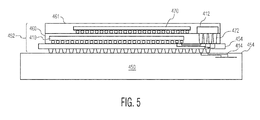
- Fig. 5 depicts a side cutaway view of another embodiment of internal electronic components of the electronic device 102 of Fig. 1 .
- the embodiment of Fig. 5 is similar to the embodiment of Fig. 4 , with the embodiment of Fig. 5 including a "package-on-package" configuration in which an additional IC 470, such as a memory IC, is packaged on top of the CPU 410.
- the electronic components of the embodiment of Fig. 5 include a circuit board 450, an RFID antenna 414, and a packaged IC 452, with the packaged IC including the CPU, the memory IC, and the RFID IC 412.
- the memory IC 470 and the RFID IC 412 are packaged above the CPU 410 in a second level package that includes internal contact pads.
- the physically secure communications channel 416 is still embedded in the substrate 454 of the packaged IC and electrically connects the CPU to the RFID IC.
- the RFID IC is electrically connected to the RFID antenna and the communications channel via conductive elements that traverse the CPU package, including conductive elements 472 that electrically connect the RFID antenna to the RFID IC and conductive elements that electrically connect the RFIC IC to the communications channel.
- the RFID IC is attached to a second level packaging surface through which the conductive elements protrude.
- the conductive elements may include, for example, copper wires, aluminum wires, or conductive glue.
- the CPU 410, the memory IC 470, and the RFID IC 412 are enclosed within first and second level encapsulants 460 and 461, respectively, such that the CPU and the RFID IC are not accessible from outside the packaged IC.
- the encapsulant may be a plastic or ceramic encapsulant as is known in the field of IC packaging. Other encapsulant materials and/or configurations are possible.
- the CPU, the memory IC, and the RFID IC are enclosed within a ceramic encapsulant that is fixed to the substrate with adhesive.
- the CPU, the memory IC, and/or the RFID IC may be partially or fully accessible from outside packaged IC.
- the communications channel 416 between the CPU 410 and the RFID IC 412 is physically secure such that the communications channel is protected from physical access by a structural barrier.
- the structural barrier includes the first and second level packaging and the substrate 454, within which the communications channel is embedded.
- Fig. 6 depicts a side cutaway view of another embodiment of internal electronic components of the electronic device 102 of Fig. 1 .
- the embodiment of Fig. 6 is similar to the embodiment of Fig. 4 , with the embodiment of Fig. 6 having the RFID IC 412 embedded within the substrate 454 of the packaged IC 452 instead of mounted on the top major surface 464 of the substrate.
- the RFID IC is electrically connected to the RFID antenna 414 via external conductive pads 456 and conductive traces 474 and electrically connected to the CPU 410 via conductive traces 476 and internal conductive pads 458.
- the CPU is attached to the substrate directly above the endpoints of the conductive traces of the communications channel.
- the communications channel 416/476 between the CPU 410 and the RFID IC 412 is physically secure such that the communications channel is protected from physical access by a structural barrier.
- the physical protection of the communications channel is at least a three-fold. First, access to the communications channel is protected by the encapsulant of the packaged IC. Second, access to the communications channel is protected by the location of the CPU directly above the endpoints of the communications channel. Third, access to the communications channel between the endpoints is protected by the fact that the conductive traces of the communications channel are embedded within the substrate. Given the configuration of Fig.
- an intruder intending to fraudulently configure the electronic device by gaining access to the communications channel would likely have to remove the encapsulant of the packaged IC and then remove the CPU from the substrate. Such structural barriers to physical access can deter attempts to fraudulently configure the electronic device. Further, removing the encapsulant and the CPU of the packaged IC to gain access to the communications channel may ultimately damage the electronic device and render the electronic device unusable for its intended purpose, thereby providing a further deterrent to fraudulent configuration.
- Fig. 7 depicts a side cutaway view of another embodiment of internal electronic components of the electronic device 102 of Fig. 1 .
- the embodiment of Fig. 7 is similar to the embodiment of Fig. 6 , with the embodiment of Fig. 7 having the RFID IC 412 located within a cavity of the circuit board 450 instead of embedded within the substrate 454 of the packaged IC 452.
- the circuit board has a cavity 480 with an elevation that is below the elevation of the top major surface 455 of the circuit board 450.
- the RFID IC is attached within the cavity directly below the packaged IC. As depicted in Fig.
- the RFID IC is electrically connected to the RFID antenna via conductive traces 474 that are embedded within the circuit board and the RFID IC is electrically connected to the external conductive pads 456 of the packaged IC by conductive traces 476 that are embedded within the circuit board.
- the packaged IC is attached to the circuit board directly above the contact points of the conductive traces of the communications channel and directly above the RFID IC such that it is difficult if not impossible to physically access the RFID IC without removing the CPU from the circuit board.
- the packaged IC may be attached to the circuit board by soldering all of the external contact pads 456 to the circuit board, creating a barrier of soldered contact pads between the RFID IC and the surrounding environment. Given the configuration of Fig.
- the communications channel between the CPU and the RFID IC is physically secure such that the communications channel is protected from physical access by a structural barrier.
- the physical protection of the communications channel is at least a three-fold.
- First, access to the RFID IC is protected because the packaged IC is attached to the circuit board directly above the RFID IC.
- Second, access to the communications channel between the endpoints at the top surface of the circuit board and the RFID IC is protected by the fact that the conductive traces of the communications channel are embedded within the circuit board. Given the configuration of Fig.
- an intruder intending to fraudulently configure the electronic device by gaining access to the communications channel would likely have to remove the packaged IC from the circuit board, which may ultimately damage the electronic device and render the electronic device unusable for its intended purpose, thereby providing a deterrent to fraudulent configuration.
- a cavity may be formed by a connection structure that is part of, or attached to, the circuit board.
- a rectangular connection structure is configured to receive the RFID IC in a central recessed location, with the packaged IC affixed on top of the connection structure and directly above the RFID IC.
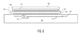
- Fig. 8 depicts a side cutaway view of another embodiment of internal electronic components of the electronic device 102 of Fig. 1 .
- the embodiment of Fig. 8 is similar to the embodiment of Fig. 6 , with the embodiment of Fig. 8 having the RFID IC 412 embedded within the circuit board 450 instead of embedded within the substrate 454 of the packaged IC 452.
- the RFID IC is electrically connected to the RFID antenna 414 via conductive traces 474 that are embedded within the circuit board and the RFID IC is electrically connected to the external conductive pads 456 of the packaged IC by conductive traces 476 that are embedded within the circuit board.
- the packaged IC is attached to the circuit board directly above the contact points of the conductive traces of the communications channel.
- the communications channel 416 between the CPU 410 and the RFID IC 412 is physically secure such that the communications channel is protected from physical access by a structural barrier and the physical protection of the communications channel is at least a three-fold.
- access to the RFID IC is protected because the RFID IC is embedded within the circuit board.
- access to the communications channel is protected by the location of the packaged IC directly above the endpoints of the communications channel.
- access to the communications channel between the endpoints is protected by the fact that the conductive traces of the communications channel are embedded within the circuit board.
- an intruder intending to fraudulently configure the electronic device by gaining access to the communications channel would have to remove the packaged IC from the circuit board, which may ultimately damage the electronic device and render the electronic device unusable for its intended purpose, thereby providing a deterrent to fraudulent configuration.
- an embodiment of a computer program product includes a computer useable storage medium to store a computer readable program.
- the computer-useable or computer-readable storage medium can be an electronic, magnetic, optical, electromagnetic, infrared, or semiconductor system (or apparatus or device).
- Examples of non-transitory computer-useable and computer-readable storage media include a semiconductor or solid state memory, magnetic tape, a removable computer diskette, a random access memory (RAM), a read-only memory (ROM), a rigid magnetic disk, and an optical disk.
- Current examples of optical disks include a compact disk with read only memory (CD-ROM), a compact disk with read/write (CD-R/W), and a digital video disk (DVD).
- embodiments of the invention may be implemented entirely in hardware or in an implementation containing both hardware and software elements.
- the software may include but is not limited to firmware, resident software, microcode, etc.
Landscapes
- Engineering & Computer Science (AREA)
- Computer Hardware Design (AREA)
- Theoretical Computer Science (AREA)
- Computer Security & Cryptography (AREA)
- General Engineering & Computer Science (AREA)
- General Physics & Mathematics (AREA)
- Physics & Mathematics (AREA)
- Software Systems (AREA)
- Microelectronics & Electronic Packaging (AREA)
- Health & Medical Sciences (AREA)
- Bioethics (AREA)
- General Health & Medical Sciences (AREA)
- Storage Device Security (AREA)
- Transceivers (AREA)
Applications Claiming Priority (1)
| Application Number | Priority Date | Filing Date | Title |
|---|---|---|---|
| US13/584,210 US20140047567A1 (en) | 2012-08-13 | 2012-08-13 | Method and system for secure configuration of an electronic device via an rfid ic |
Publications (2)
| Publication Number | Publication Date |
|---|---|
| EP2698746A2 true EP2698746A2 (de) | 2014-02-19 |
| EP2698746A3 EP2698746A3 (de) | 2018-04-04 |
Family
ID=48790175
Family Applications (1)
| Application Number | Title | Priority Date | Filing Date |
|---|---|---|---|
| EP13173713.2A Withdrawn EP2698746A3 (de) | 2012-08-13 | 2013-06-26 | Verfahren und System zur sicheren Konfiguration einer elektronischen Vorrichtung über ein RFID IC |
Country Status (2)
| Country | Link |
|---|---|
| US (1) | US20140047567A1 (de) |
| EP (1) | EP2698746A3 (de) |
Families Citing this family (7)
| Publication number | Priority date | Publication date | Assignee | Title |
|---|---|---|---|---|
| US9092712B2 (en) * | 2012-11-02 | 2015-07-28 | Flextronics Ap, Llc | Embedded high frequency RFID |
| US9053405B1 (en) | 2013-08-27 | 2015-06-09 | Flextronics Ap, Llc | Printed RFID circuit |
| US9967749B2 (en) * | 2013-09-26 | 2018-05-08 | Dell Products L.P. | Secure near field communication server information handling system support |
| US10528357B2 (en) * | 2014-01-17 | 2020-01-07 | L3 Technologies, Inc. | Web-based recorder configuration utility |
| US9560746B1 (en) | 2014-01-24 | 2017-01-31 | Multek Technologies, Ltd. | Stress relief for rigid components on flexible circuits |
| US10256974B1 (en) * | 2018-04-25 | 2019-04-09 | Blockchain Asics Llc | Cryptographic ASIC for key hierarchy enforcement |
| WO2025236047A1 (en) * | 2024-05-17 | 2025-11-20 | ResMed Pty Ltd | Systems and methods for setup, maintenance, and/or use of respiratory therapy devices |
Citations (4)
| Publication number | Priority date | Publication date | Assignee | Title |
|---|---|---|---|---|
| US6249227B1 (en) * | 1998-01-05 | 2001-06-19 | Intermec Ip Corp. | RFID integrated in electronic assets |
| US20060022799A1 (en) * | 2004-07-29 | 2006-02-02 | Ari Juels | Methods and apparatus for RFID device authentication |
| US20060087883A1 (en) * | 2004-10-08 | 2006-04-27 | Irvine Sensors Corporation | Anti-tamper module |
| US7825776B2 (en) * | 2006-08-17 | 2010-11-02 | Intel Corporation | Device configuration with RFID |
Family Cites Families (5)
| Publication number | Priority date | Publication date | Assignee | Title |
|---|---|---|---|---|
| US7675151B1 (en) * | 2005-06-01 | 2010-03-09 | Rockwell Collins, Inc. | Silicon-based packaging for electronic devices |
| DE102005043657B4 (de) * | 2005-09-13 | 2011-12-15 | Infineon Technologies Ag | Chipmodul, Verfahren zur Verkapselung eines Chips und Verwendung eines Verkapselungsmaterials |
| US7685263B2 (en) * | 2006-12-19 | 2010-03-23 | Blue Coat Systems, Inc. | Method and system for configuring a device with a wireless mobile configurator |
| KR20120035394A (ko) * | 2010-10-05 | 2012-04-16 | 삼성전자주식회사 | 수직구조의 전송선로 트랜지션 및 랜드 그리드 어레이 접합를 이용한 단일 칩 패키지를 위한 장치 |
| KR101711048B1 (ko) * | 2010-10-07 | 2017-03-02 | 삼성전자 주식회사 | 차폐막을 포함하는 반도체 장치 및 제조 방법 |
-
2012
- 2012-08-13 US US13/584,210 patent/US20140047567A1/en not_active Abandoned
-
2013
- 2013-06-26 EP EP13173713.2A patent/EP2698746A3/de not_active Withdrawn
Patent Citations (4)
| Publication number | Priority date | Publication date | Assignee | Title |
|---|---|---|---|---|
| US6249227B1 (en) * | 1998-01-05 | 2001-06-19 | Intermec Ip Corp. | RFID integrated in electronic assets |
| US20060022799A1 (en) * | 2004-07-29 | 2006-02-02 | Ari Juels | Methods and apparatus for RFID device authentication |
| US20060087883A1 (en) * | 2004-10-08 | 2006-04-27 | Irvine Sensors Corporation | Anti-tamper module |
| US7825776B2 (en) * | 2006-08-17 | 2010-11-02 | Intel Corporation | Device configuration with RFID |
Also Published As
| Publication number | Publication date |
|---|---|
| EP2698746A3 (de) | 2018-04-04 |
| US20140047567A1 (en) | 2014-02-13 |
Similar Documents
| Publication | Publication Date | Title |
|---|---|---|
| EP2698746A2 (de) | Verfahren und System zur sicheren Konfiguration einer elektronischen Vorrichtung über ein RFID IC | |
| US10078599B2 (en) | Application access control method and electronic apparatus implementing the same | |
| EP3108613B1 (de) | Verfahren und vorrichtung zur authentifizierung von client-berechtigungsnachweisen | |
| EP3131032B1 (de) | Authentifizierungsvorrichtung und -verfahren | |
| CN104160652B (zh) | 用于使用一次性密码的分布式离线登录的方法和系统 | |
| JP6937541B2 (ja) | 切り替え可能な内部接続役割を有するpos装置 | |
| CN103988185A (zh) | 安全的重放保护存储 | |
| CN101506815A (zh) | 用于安全系统的双处理器结构 | |
| CN101010677A (zh) | 用于交换数据的便携式存储设备和方法 | |
| KR102180529B1 (ko) | 어플리케이션 접근 제어 방법 및 이를 구현하는 전자 장치 | |
| CN104937606A (zh) | 近场通信(nfc)交易中的数据保护 | |
| KR20150011377A (ko) | 전자 인증 클라이언트 시스템 및 프로세싱 방법, 그리고 전자 인증 시스템 및 방법 | |
| US20210141946A1 (en) | System, device and method for protecting information of a payment transaction using tamper-resistant portable stick computer device | |
| US9331855B2 (en) | Apparatus, system, and method for providing attribute identity control associated with a processor | |
| CN112287360A (zh) | 电子装置以及该电子装置的操作方法 | |
| US20190042706A1 (en) | Display of protected content using trusted execution environment | |
| US9536116B2 (en) | Active component embedded in cable | |
| CN1971452B (zh) | 时间数据检验单元、用于检验时间数据的电子设备和方法 | |
| JP4996625B2 (ja) | 第1の通信機と第2の通信機とのあいだでの共通鍵の指定方法、および、第1の通信機と第2の通信機とのあいだでの共通鍵の指定装置 | |
| US20150095223A1 (en) | Electronic payment device | |
| CN112085505B (zh) | 人脸支付方法 | |
| US20130117864A1 (en) | Authentication system | |
| TWM612447U (zh) | 用於身分驗證的設備端和用於獲得產品權限的使用端 | |
| CN114595488A (zh) | 数据交换的管理方法、电子设备及存储介质 | |
| US12499200B2 (en) | Secure component verification using nfc |
Legal Events
| Date | Code | Title | Description |
|---|---|---|---|
| AK | Designated contracting states |
Kind code of ref document: A2 Designated state(s): AL AT BE BG CH CY CZ DE DK EE ES FI FR GB GR HR HU IE IS IT LI LT LU LV MC MK MT NL NO PL PT RO RS SE SI SK SM TR |
|
| AX | Request for extension of the european patent |
Extension state: BA ME |
|
| PUAI | Public reference made under article 153(3) epc to a published international application that has entered the european phase |
Free format text: ORIGINAL CODE: 0009012 |
|
| 17P | Request for examination filed |
Effective date: 20140326 |
|
| RIC1 | Information provided on ipc code assigned before grant |
Ipc: H01L 23/00 20060101ALI20170906BHEP Ipc: H05K 1/02 20060101ALI20170906BHEP Ipc: G06F 21/86 20130101ALI20170906BHEP Ipc: H01L 25/065 20060101ALI20170906BHEP Ipc: G06F 21/62 20130101ALI20170906BHEP Ipc: H05K 1/18 20060101ALI20170906BHEP Ipc: G06F 21/57 20130101ALI20170906BHEP Ipc: G06K 19/073 20060101AFI20170906BHEP Ipc: H04W 12/02 20090101ALI20170906BHEP Ipc: H04L 29/06 20060101ALI20170906BHEP Ipc: G06F 21/60 20130101ALI20170906BHEP Ipc: H01L 23/66 20060101ALI20170906BHEP Ipc: H01L 25/10 20060101ALI20170906BHEP Ipc: H05K 1/16 20060101ALI20170906BHEP |
|
| PUAL | Search report despatched |
Free format text: ORIGINAL CODE: 0009013 |
|
| AK | Designated contracting states |
Kind code of ref document: A3 Designated state(s): AL AT BE BG CH CY CZ DE DK EE ES FI FR GB GR HR HU IE IS IT LI LT LU LV MC MK MT NL NO PL PT RO RS SE SI SK SM TR |
|
| AX | Request for extension of the european patent |
Extension state: BA ME |
|
| RIC1 | Information provided on ipc code assigned before grant |
Ipc: H05K 1/18 20060101ALI20180227BHEP Ipc: G06F 21/60 20130101ALI20180227BHEP Ipc: H04W 12/02 20090101ALI20180227BHEP Ipc: H01L 25/065 20060101ALI20180227BHEP Ipc: H05K 1/16 20060101ALI20180227BHEP Ipc: H01L 23/00 20060101ALI20180227BHEP Ipc: G06K 19/073 20060101AFI20180227BHEP Ipc: H05K 1/02 20060101ALI20180227BHEP Ipc: H01L 23/66 20060101ALI20180227BHEP Ipc: H01L 25/10 20060101ALI20180227BHEP Ipc: G06F 21/62 20130101ALI20180227BHEP Ipc: H04L 29/06 20060101ALI20180227BHEP Ipc: G06F 21/57 20130101ALI20180227BHEP Ipc: G06F 21/86 20130101ALI20180227BHEP |
|
| RBV | Designated contracting states (corrected) |
Designated state(s): AL AT BE BG CH CY CZ DE DK EE ES FI FR GB GR HR HU IE IS IT LI LT LU LV MC MK MT NL NO PL PT RO RS SE SI SK SM TR |
|
| 17Q | First examination report despatched |
Effective date: 20191001 |
|
| STAA | Information on the status of an ep patent application or granted ep patent |
Free format text: STATUS: THE APPLICATION IS DEEMED TO BE WITHDRAWN |
|
| 18D | Application deemed to be withdrawn |
Effective date: 20200212 |