EP2695233B1 - Flat-conductor connection element for an antenna structure - Google Patents
Flat-conductor connection element for an antenna structure Download PDFInfo
- Publication number
- EP2695233B1 EP2695233B1 EP12706820.3A EP12706820A EP2695233B1 EP 2695233 B1 EP2695233 B1 EP 2695233B1 EP 12706820 A EP12706820 A EP 12706820A EP 2695233 B1 EP2695233 B1 EP 2695233B1
- Authority
- EP
- European Patent Office
- Prior art keywords
- pane
- shield
- flat conductor
- conductor
- dielectric layer
- Prior art date
- Legal status (The legal status is an assumption and is not a legal conclusion. Google has not performed a legal analysis and makes no representation as to the accuracy of the status listed.)
- Active
Links
- 239000004020 conductor Substances 0.000 title claims description 179
- 239000010410 layer Substances 0.000 claims description 98
- 229910052751 metal Inorganic materials 0.000 claims description 22
- 239000002184 metal Substances 0.000 claims description 22
- 239000012790 adhesive layer Substances 0.000 claims description 19
- 239000000853 adhesive Substances 0.000 claims description 18
- 230000001070 adhesive effect Effects 0.000 claims description 18
- 239000002131 composite material Substances 0.000 claims description 18
- 229920003023 plastic Polymers 0.000 claims description 12
- 239000004033 plastic Substances 0.000 claims description 12
- 239000011888 foil Substances 0.000 claims description 11
- 239000004642 Polyimide Substances 0.000 claims description 10
- 229920001721 polyimide Polymers 0.000 claims description 10
- 239000011521 glass Substances 0.000 claims description 9
- -1 polyethylene Polymers 0.000 claims description 9
- 229920000139 polyethylene terephthalate Polymers 0.000 claims description 8
- 239000005020 polyethylene terephthalate Substances 0.000 claims description 8
- 239000004945 silicone rubber Substances 0.000 claims description 8
- 238000004519 manufacturing process Methods 0.000 claims description 7
- 239000000203 mixture Substances 0.000 claims description 7
- 239000004952 Polyamide Substances 0.000 claims description 6
- 229920002647 polyamide Polymers 0.000 claims description 6
- 229920002379 silicone rubber Polymers 0.000 claims description 6
- 239000004698 Polyethylene Substances 0.000 claims description 5
- 229920000573 polyethylene Polymers 0.000 claims description 5
- RYGMFSIKBFXOCR-UHFFFAOYSA-N Copper Chemical compound [Cu] RYGMFSIKBFXOCR-UHFFFAOYSA-N 0.000 claims description 4
- 239000004743 Polypropylene Substances 0.000 claims description 4
- 229920001577 copolymer Polymers 0.000 claims description 4
- 229910052802 copper Inorganic materials 0.000 claims description 4
- 239000010949 copper Substances 0.000 claims description 4
- 229920001707 polybutylene terephthalate Polymers 0.000 claims description 4
- 229920000647 polyepoxide Polymers 0.000 claims description 4
- 229920001155 polypropylene Polymers 0.000 claims description 4
- 229920001343 polytetrafluoroethylene Polymers 0.000 claims description 4
- 239000004814 polyurethane Substances 0.000 claims description 4
- 229920001169 thermoplastic Polymers 0.000 claims description 4
- 239000004416 thermosoftening plastic Substances 0.000 claims description 4
- NIXOWILDQLNWCW-UHFFFAOYSA-M Acrylate Chemical compound [O-]C(=O)C=C NIXOWILDQLNWCW-UHFFFAOYSA-M 0.000 claims description 3
- 239000004417 polycarbonate Substances 0.000 claims description 3
- 229920000515 polycarbonate Polymers 0.000 claims description 3
- 229920002635 polyurethane Polymers 0.000 claims description 3
- 239000004800 polyvinyl chloride Substances 0.000 claims description 3
- 239000004925 Acrylic resin Substances 0.000 claims description 2
- 229920000178 Acrylic resin Polymers 0.000 claims description 2
- VVQNEPGJFQJSBK-UHFFFAOYSA-N Methyl methacrylate Chemical compound COC(=O)C(C)=C VVQNEPGJFQJSBK-UHFFFAOYSA-N 0.000 claims description 2
- 239000005062 Polybutadiene Substances 0.000 claims description 2
- BQCADISMDOOEFD-UHFFFAOYSA-N Silver Chemical compound [Ag] BQCADISMDOOEFD-UHFFFAOYSA-N 0.000 claims description 2
- 239000004830 Super Glue Substances 0.000 claims description 2
- ATJFFYVFTNAWJD-UHFFFAOYSA-N Tin Chemical compound [Sn] ATJFFYVFTNAWJD-UHFFFAOYSA-N 0.000 claims description 2
- 229920000180 alkyd Polymers 0.000 claims description 2
- 229910052782 aluminium Inorganic materials 0.000 claims description 2
- XAGFODPZIPBFFR-UHFFFAOYSA-N aluminium Chemical compound [Al] XAGFODPZIPBFFR-UHFFFAOYSA-N 0.000 claims description 2
- 239000003822 epoxy resin Substances 0.000 claims description 2
- FGBJXOREULPLGL-UHFFFAOYSA-N ethyl cyanoacrylate Chemical compound CCOC(=O)C(=C)C#N FGBJXOREULPLGL-UHFFFAOYSA-N 0.000 claims description 2
- PCHJSUWPFVWCPO-UHFFFAOYSA-N gold Chemical compound [Au] PCHJSUWPFVWCPO-UHFFFAOYSA-N 0.000 claims description 2
- 239000010931 gold Substances 0.000 claims description 2
- 229910052737 gold Inorganic materials 0.000 claims description 2
- 229920002857 polybutadiene Polymers 0.000 claims description 2
- 239000011112 polyethylene naphthalate Substances 0.000 claims description 2
- 229920000098 polyolefin Polymers 0.000 claims description 2
- 229920002631 room-temperature vulcanizate silicone Polymers 0.000 claims description 2
- 239000013464 silicone adhesive Substances 0.000 claims description 2
- 229910052709 silver Inorganic materials 0.000 claims description 2
- 239000004332 silver Substances 0.000 claims description 2
- 239000011135 tin Substances 0.000 claims description 2
- 229910052718 tin Inorganic materials 0.000 claims description 2
- XLYOFNOQVPJJNP-UHFFFAOYSA-N water Substances O XLYOFNOQVPJJNP-UHFFFAOYSA-N 0.000 claims description 2
- 239000004810 polytetrafluoroethylene Substances 0.000 claims 2
- 239000004593 Epoxy Substances 0.000 claims 1
- BLRPTPMANUNPDV-UHFFFAOYSA-N Silane Chemical compound [SiH4] BLRPTPMANUNPDV-UHFFFAOYSA-N 0.000 claims 1
- 238000004132 cross linking Methods 0.000 claims 1
- 125000003700 epoxy group Chemical group 0.000 claims 1
- 150000002978 peroxides Chemical class 0.000 claims 1
- 229920000642 polymer Polymers 0.000 claims 1
- 229920006254 polymer film Polymers 0.000 claims 1
- 229910000077 silane Inorganic materials 0.000 claims 1
- 239000002966 varnish Substances 0.000 claims 1
- 239000003990 capacitor Substances 0.000 description 9
- 239000011248 coating agent Substances 0.000 description 8
- 238000000576 coating method Methods 0.000 description 8
- 230000008878 coupling Effects 0.000 description 8
- 238000010168 coupling process Methods 0.000 description 8
- 238000005859 coupling reaction Methods 0.000 description 8
- 239000000463 material Substances 0.000 description 6
- 238000005259 measurement Methods 0.000 description 6
- 238000010586 diagram Methods 0.000 description 5
- 238000000034 method Methods 0.000 description 5
- 229910000679 solder Inorganic materials 0.000 description 5
- 239000000758 substrate Substances 0.000 description 5
- 239000003989 dielectric material Substances 0.000 description 4
- 239000010408 film Substances 0.000 description 4
- 238000005516 engineering process Methods 0.000 description 3
- 238000009413 insulation Methods 0.000 description 3
- 230000005855 radiation Effects 0.000 description 3
- 230000008054 signal transmission Effects 0.000 description 3
- 239000013039 cover film Substances 0.000 description 2
- 238000010438 heat treatment Methods 0.000 description 2
- 239000004922 lacquer Substances 0.000 description 2
- 230000000873 masking effect Effects 0.000 description 2
- 239000002985 plastic film Substances 0.000 description 2
- 229920006255 plastic film Polymers 0.000 description 2
- 229920003229 poly(methyl methacrylate) Polymers 0.000 description 2
- 229920002037 poly(vinyl butyral) polymer Polymers 0.000 description 2
- 239000004926 polymethyl methacrylate Substances 0.000 description 2
- 230000002787 reinforcement Effects 0.000 description 2
- 229920002799 BoPET Polymers 0.000 description 1
- 239000004793 Polystyrene Substances 0.000 description 1
- 241001074085 Scophthalmus aquosus Species 0.000 description 1
- 230000006750 UV protection Effects 0.000 description 1
- 208000027418 Wounds and injury Diseases 0.000 description 1
- 238000004026 adhesive bonding Methods 0.000 description 1
- 230000002238 attenuated effect Effects 0.000 description 1
- 230000005540 biological transmission Effects 0.000 description 1
- 239000012876 carrier material Substances 0.000 description 1
- 239000000919 ceramic Substances 0.000 description 1
- DGLFSNZWRYADFC-UHFFFAOYSA-N chembl2334586 Chemical compound C1CCC2=CN=C(N)N=C2C2=C1NC1=CC=C(C#CC(C)(O)C)C=C12 DGLFSNZWRYADFC-UHFFFAOYSA-N 0.000 description 1
- 238000010276 construction Methods 0.000 description 1
- 230000007797 corrosion Effects 0.000 description 1
- 238000005260 corrosion Methods 0.000 description 1
- 230000006378 damage Effects 0.000 description 1
- 238000010292 electrical insulation Methods 0.000 description 1
- 239000012799 electrically-conductive coating Substances 0.000 description 1
- 239000005038 ethylene vinyl acetate Substances 0.000 description 1
- 238000001125 extrusion Methods 0.000 description 1
- 230000002349 favourable effect Effects 0.000 description 1
- 239000005357 flat glass Substances 0.000 description 1
- 239000005329 float glass Substances 0.000 description 1
- 208000014674 injury Diseases 0.000 description 1
- 239000011810 insulating material Substances 0.000 description 1
- 238000002955 isolation Methods 0.000 description 1
- 230000013011 mating Effects 0.000 description 1
- 239000012811 non-conductive material Substances 0.000 description 1
- 229920000728 polyester Polymers 0.000 description 1
- 238000007639 printing Methods 0.000 description 1
- 230000004224 protection Effects 0.000 description 1
- 238000007650 screen-printing Methods 0.000 description 1
- 238000005476 soldering Methods 0.000 description 1
- 125000006850 spacer group Chemical group 0.000 description 1
- 239000000126 substance Substances 0.000 description 1
- 230000037072 sun protection Effects 0.000 description 1
- 230000028016 temperature homeostasis Effects 0.000 description 1
- 210000002105 tongue Anatomy 0.000 description 1
- 239000012780 transparent material Substances 0.000 description 1
- 238000011144 upstream manufacturing Methods 0.000 description 1
Images


Classifications
-
- H—ELECTRICITY
- H01—ELECTRIC ELEMENTS
- H01Q—ANTENNAS, i.e. RADIO AERIALS
- H01Q1/00—Details of, or arrangements associated with, antennas
- H01Q1/12—Supports; Mounting means
-
- H—ELECTRICITY
- H01—ELECTRIC ELEMENTS
- H01B—CABLES; CONDUCTORS; INSULATORS; SELECTION OF MATERIALS FOR THEIR CONDUCTIVE, INSULATING OR DIELECTRIC PROPERTIES
- H01B7/00—Insulated conductors or cables characterised by their form
- H01B7/08—Flat or ribbon cables
- H01B7/0861—Flat or ribbon cables comprising one or more screens
-
- B—PERFORMING OPERATIONS; TRANSPORTING
- B32—LAYERED PRODUCTS
- B32B—LAYERED PRODUCTS, i.e. PRODUCTS BUILT-UP OF STRATA OF FLAT OR NON-FLAT, e.g. CELLULAR OR HONEYCOMB, FORM
- B32B17/00—Layered products essentially comprising sheet glass, or glass, slag, or like fibres
- B32B17/06—Layered products essentially comprising sheet glass, or glass, slag, or like fibres comprising glass as the main or only constituent of a layer, next to another layer of a specific material
- B32B17/10—Layered products essentially comprising sheet glass, or glass, slag, or like fibres comprising glass as the main or only constituent of a layer, next to another layer of a specific material of synthetic resin
- B32B17/10005—Layered products essentially comprising sheet glass, or glass, slag, or like fibres comprising glass as the main or only constituent of a layer, next to another layer of a specific material of synthetic resin laminated safety glass or glazing
- B32B17/10009—Layered products essentially comprising sheet glass, or glass, slag, or like fibres comprising glass as the main or only constituent of a layer, next to another layer of a specific material of synthetic resin laminated safety glass or glazing characterized by the number, the constitution or treatment of glass sheets
- B32B17/10036—Layered products essentially comprising sheet glass, or glass, slag, or like fibres comprising glass as the main or only constituent of a layer, next to another layer of a specific material of synthetic resin laminated safety glass or glazing characterized by the number, the constitution or treatment of glass sheets comprising two outer glass sheets
-
- B—PERFORMING OPERATIONS; TRANSPORTING
- B32—LAYERED PRODUCTS
- B32B—LAYERED PRODUCTS, i.e. PRODUCTS BUILT-UP OF STRATA OF FLAT OR NON-FLAT, e.g. CELLULAR OR HONEYCOMB, FORM
- B32B17/00—Layered products essentially comprising sheet glass, or glass, slag, or like fibres
- B32B17/06—Layered products essentially comprising sheet glass, or glass, slag, or like fibres comprising glass as the main or only constituent of a layer, next to another layer of a specific material
- B32B17/10—Layered products essentially comprising sheet glass, or glass, slag, or like fibres comprising glass as the main or only constituent of a layer, next to another layer of a specific material of synthetic resin
- B32B17/10005—Layered products essentially comprising sheet glass, or glass, slag, or like fibres comprising glass as the main or only constituent of a layer, next to another layer of a specific material of synthetic resin laminated safety glass or glazing
- B32B17/10165—Functional features of the laminated safety glass or glazing
- B32B17/10293—Edge features, e.g. inserts or holes
-
- H—ELECTRICITY
- H01—ELECTRIC ELEMENTS
- H01B—CABLES; CONDUCTORS; INSULATORS; SELECTION OF MATERIALS FOR THEIR CONDUCTIVE, INSULATING OR DIELECTRIC PROPERTIES
- H01B13/00—Apparatus or processes specially adapted for manufacturing conductors or cables
- H01B13/06—Insulating conductors or cables
-
- H—ELECTRICITY
- H01—ELECTRIC ELEMENTS
- H01Q—ANTENNAS, i.e. RADIO AERIALS
- H01Q1/00—Details of, or arrangements associated with, antennas
- H01Q1/12—Supports; Mounting means
- H01Q1/1271—Supports; Mounting means for mounting on windscreens
-
- H—ELECTRICITY
- H01—ELECTRIC ELEMENTS
- H01Q—ANTENNAS, i.e. RADIO AERIALS
- H01Q1/00—Details of, or arrangements associated with, antennas
- H01Q1/52—Means for reducing coupling between antennas; Means for reducing coupling between an antenna and another structure
-
- H—ELECTRICITY
- H01—ELECTRIC ELEMENTS
- H01Q—ANTENNAS, i.e. RADIO AERIALS
- H01Q1/00—Details of, or arrangements associated with, antennas
- H01Q1/52—Means for reducing coupling between antennas; Means for reducing coupling between an antenna and another structure
- H01Q1/526—Electromagnetic shields
-
- H—ELECTRICITY
- H01—ELECTRIC ELEMENTS
- H01R—ELECTRICALLY-CONDUCTIVE CONNECTIONS; STRUCTURAL ASSOCIATIONS OF A PLURALITY OF MUTUALLY-INSULATED ELECTRICAL CONNECTING ELEMENTS; COUPLING DEVICES; CURRENT COLLECTORS
- H01R12/00—Structural associations of a plurality of mutually-insulated electrical connecting elements, specially adapted for printed circuits, e.g. printed circuit boards [PCB], flat or ribbon cables, or like generally planar structures, e.g. terminal strips, terminal blocks; Coupling devices specially adapted for printed circuits, flat or ribbon cables, or like generally planar structures; Terminals specially adapted for contact with, or insertion into, printed circuits, flat or ribbon cables, or like generally planar structures
- H01R12/50—Fixed connections
-
- Y—GENERAL TAGGING OF NEW TECHNOLOGICAL DEVELOPMENTS; GENERAL TAGGING OF CROSS-SECTIONAL TECHNOLOGIES SPANNING OVER SEVERAL SECTIONS OF THE IPC; TECHNICAL SUBJECTS COVERED BY FORMER USPC CROSS-REFERENCE ART COLLECTIONS [XRACs] AND DIGESTS
- Y10—TECHNICAL SUBJECTS COVERED BY FORMER USPC
- Y10T—TECHNICAL SUBJECTS COVERED BY FORMER US CLASSIFICATION
- Y10T29/00—Metal working
- Y10T29/49—Method of mechanical manufacture
- Y10T29/49002—Electrical device making
- Y10T29/49016—Antenna or wave energy "plumbing" making
- Y10T29/49018—Antenna or wave energy "plumbing" making with other electrical component
Definitions
- the invention relates to a disk arrangement with a flat conductor connection element for an antenna structure and to a method for the production thereof.
- the built-in conventional vehicle windscreens antennas are of the type line emitter.
- the term line emitter here describes a line-shaped antenna which is suitable both for receiving and for transmitting electromagnetic waves.
- Line radiators have a geometric length that exceeds their geometric width by several orders of magnitude.
- the geometric length of a line radiator is the distance between antenna base and antenna tip, the geometric width is the vertical dimension.
- length / width ⁇ 100 the following relationship usually applies: length / width ⁇ 100.
- line radiators for their geometric height which is to be understood as meaning a dimension that is both perpendicular to the length and perpendicular to the width, with the context as a rule Length / height ⁇ 100 applies.
- Line radiators may also be used in windshields of motor vehicles, provided that they do not impair the driver's visibility in accordance with legal requirements. This can be achieved for example by fine wires with a diameter of typically 10 to 150 microns.
- line emitters in the range of the terrestrial bands II to V a satisfactory antenna signal can be provided.
- ITU I nternational T elecommunication U nion
- band II 87.5 to 100 MHz, Volume III: 162-230 MHz
- Band IV 470-582 MHz
- Band V 582-960 MHz
- line sources in the upstream frequency range of band I can be used (41-68 MHz) can no longer achieve a satisfactory reception performance. The same applies to frequencies below Band I.
- planar antennas or planar antennas are suitable both for receiving and for transmitting electromagnetic waves and are also referred to below as surface radiators.
- Surface radiators are based on a planar, electrically conductive, transparent coating and are for example from the publications DE 101 06 125 A1 . DE 103 19 606 A1 . EP 0 720 249 A2 . US 2003/0112190 A1 and DE 198 32 228 C2 known.
- the conductive coating is galvanically or capacitively coupled to a coupling electrode and the antenna signal is provided in the edge region of the disk at the so-called antenna base point.
- connection conductors usually unshielded stranded wires or flat conductors are used. These have a relatively low ohmic resistance and cause only low ohmic power losses. Such unshielded stranded wires or flat conductors do not allow a defined signal transmission, since unavoidable position tolerances can lead to undefined couplings with the electrically conductive vehicle body or adjacent conductors, so that the fluctuation range of important antenna properties such as bandwidth, efficiency and line impedance is relatively large. Furthermore, such unshielded connection conductors easily coupled electromagnetic interference into the system and forwarded to the antenna amplifier.
- US 3,459,879 A discloses a flexible multicore flat conductor.
- the individual wires are either arranged in pairs with a ground line or have a common unilateral, flat ground line.
- connection surfaces of a plurality of antenna elements including shielding and grounding lines, are brought together locally adjacent to one another at a location in the edge region of the pane.
- the connection surfaces of the connection element are soldered to the connection surfaces of the glass pane.
- DE 10 2004 056 866 A1 describes a flat conductor with a plurality of conductor tracks, of which at least one is designed as a grounding conductor and connected to a shield.
- the flat conductor can be easily and inexpensively manufactured by an extrusion process.
- DE 103 51 488 A1 discloses an antenna arrangement for transmitting and receiving electromagnetic signals, the antenna arrangement comprising a planar carrier substrate of dielectric material.
- a first conductor track is applied, which has at its one end a contact point for input and output of the signals and at its opposite end a first dipole.
- a second conductor track is applied, which has at its one end a contact point for introducing or removing the signals and at its opposite end a second dipole.
- the first and second dipoles form a cross dipole.
- a window pane antenna whose main element is formed by a light-transparent transparent and in a region of the window pane applied thin electrically conductive layer and the conductive surface thus formed is fixed to the window glass.
- the conductive surface applied to the windowpane is formed from a limited conductive layer with non-negligible surface resistance.
- a substantially areally equipped electrode made of conductive material for high-frequency connection to this layer is formed, which is connected at least in the region of its boundary with the limited conductive surface high-frequency loss.
- DE 103 01 352 B3 discloses a solder connection element for at least one contact surface of an electrical conductor to be soldered to a conductor pattern provided on a substrate.
- the electrical conductor is covered at least on the side facing the substrate by an insulating cover film.
- the cover film is provided in the region of the contact surface with a recess, the edge of which surrounds the contact surface.
- WO 2009/015975 A1 describes a multicore flat conductor with a solder connection element for contacting electrically conductive structures, for example on a glass pane.
- the solder terminal includes an adhesive in the area around each pad to be soldered to fix the position of the solder pad and to prevent molten solder shorts.
- DE 202 10 286 U1 describes an adapter in the form of a flexible connecting element for connecting electrically conductive structures on motor vehicle window panes to further networks outside the panes.
- the electrically conductive structures are, for example, antennas.
- the adapter consists of a flexible, film-like carrier material on the conductor tracks run.
- the adapter comprises a shoe made of non-conductive material with metallic spring tongues, which are pressed onto contact surfaces of the electrically conductive structures.
- FR 2 913 141 A3 describes a flexible flat conductor for contacting electrically conductive structures on the surface of a disk.
- the individual conductor tracks run parallel next to one another and are arranged between two plastic films, wherein one of the plastic films is connected to the disk via an adhesive surface.
- DE 20 2004 019286 U1 discloses a flat conductor external connection element for window panes with at least one electrical or electrically connected to or in the window pane and connected to the edge of the discs out across the outwardly extending trace and a surrounding insulation, which is provided with a local reinforcement against mechanical wear ,
- the reinforcement consists of a smooth-surfaced and preferably superficial injury self-healing material that adheres to the insulation.
- the object of the present invention is to provide an antenna plate with a flat conductor connection element with improved signal transmission and low susceptibility to spurious signals.
- the antenna plate with flat conductor connection element should also be simple and inexpensive to manufacture, have a simple connection technology and be insensitive to positional tolerances when installed in a metallic frame or a vehicle body.
- the antenna amplifier is electrically connected to the electrically conductive vehicle body, wherein a high-frequency-technically effective reference potential, referred to below as reference ground, for the antenna signal is predetermined by this electrical connection.
- the usable antenna voltage results from the difference between the potential of the antenna signal and the potential of the reference ground.
- the conductor track is electrically conductively connected to the antenna structure via a connection surface, preferably galvanically or capacitively.
- the flat conductor runs over the edge of the disc to the outside. Outside the pane, the flat conductor extends at least partially adjacent to a metallic frame. The shield is thereby capacitively coupled via the metallic frame with a reference ground.
- the different layers of the flat conductor can be glued together by additional adhesive layers.
- the shield between the conductor track and the metallic frame is arranged.
- the metallic frame is not part of the flat conductor connection element but, for example, part of a window frame or a vehicle body.
- the shield, the second dielectric layer and a portion of the metallic frame form a capacitor arrangement over which the shield is capacitively coupled to the metallic frame.
- the shielding of the flat conductor extends over at least 50%, preferably over at least 75% and particularly preferably over at least 90% of the surface of the flat conductor outside the pane.
- Surface of the flat conductor means in this case the surface of a planar side of the flat conductor.
- the shield may also be arranged in the region in or on the disk for improving the shielding.
- the metallic frame comprises a vehicle body or a movable metallic frame, in particular a metallic window frame.
- the metallic frame does not necessarily have to be closed around the outer edge of the disc.
- a metallic frame according to the invention also includes a metallic and / or electrically conductive portion, such as a bar, an L-shaped or a U-shaped frame, which can serve as a reference ground of the antenna structure.
- the shield is arranged in the region of an area of 30 mm 2 to 200 mm 2 at a distance of 0.02 mm to 2 mm from the metallic frame.
- the base layer, the first dielectric layer and / or the second dielectric layer have a relative permittivity of from 1 to 6, preferably from 2 to 4, and more preferably from 3 to 3.5.
- the capacitance of the capacitor is from 5 nF to 10 pF and preferably from 0.1 nF to 2 nF.
- a high pass is formed. Via the high-pass electromagnetic interference radiation is conducted above the cut-off frequency fG of the high-pass filter from the shield to the reference ground.
- the cut-off frequency of the signal transmission from the shield to the reference ground is from 20 MHz to 1000 MHz.
- the base layer, the first dielectric layer and / or the second dielectric layer contains a plastic, preferably polyimide (PI), polyamide (PA), polyethylene (PE), polypropene (PP), polybutylene terephthalate (PBT ), Polycarbonate (PC), polyethylene terephthalate (PET), polyethylene naphthalate (PEN), polybutadiene, polyvinyl chloride (PVC) or polytetrafluoroethene (PTFE), and mixtures and / or copolymers thereof.
- PI polyimide
- PA polyamide
- PE polyethylene
- PP polypropene
- PBT polybutylene terephthalate
- PC Polycarbonate
- PET polyethylene terephthalate
- PEN polyethylene naphthalate
- PVC polyvinyl chloride
- PTFE polytetrafluoroethene
- the base layer, the first dielectric layer and / or the second dielectric layer can also be a lacquer layer, preferably alkyd resin, acrylic resin, epoxy resin or polyurethane, or an adhesive, preferably acrylate adhesive, methyl methacrylate adhesive, Polyuerthane, polyolefins, cyanoacrylate adhesive, polyepoxides, silicone adhesive and / or Silanvernetzender Polymeric adhesive, RTV silicone rubber, HTV silicone rubber, peroxidischvernetzten silicone rubber and / or addition-crosslinked silicone rubber, and mixtures and / or copolymers thereof.
- a lacquer layer preferably alkyd resin, acrylic resin, epoxy resin or polyurethane, or an adhesive, preferably acrylate adhesive, methyl methacrylate adhesive, Polyuerthane, polyolefins, cyanoacrylate adhesive, polyepoxides, silicone adhesive and / or Silanvernetzender Polymeric adhesive, RTV silicone rubber, HTV silicone rubber, peroxidischvernetzten silicone rubber and
- the second dielectric layer can also contain a gas, preferably air, wherein the distance between the shield and the metallic frame, for example formed by spacers.
- the second dielectric layer can be formed by a plastic layer or a lacquer layer on the metallic frame, for example a color layer on the vehicle body.
- the disk contains a single disk or a composite disk.
- the single pane or the individual panes of the composite pane contain, for example, a glass and / or a plastic.
- the conductor track and / or the shield contains a metal foil, a metallized plastic foil, an electrically conductive plastic foil or a metal wire mesh.
- the track may also contain a metal wire.
- the conductor track and / or the shield preferably contain an electrically highly conductive metal, particularly preferably copper, aluminum, tin, gold, silver or mixtures thereof.
- the shield has a greater width than the width of the conductor track.
- the ratio between the width of the shield and the width of the printed conductor determines the impedance of the printed circuit and is from 2: 1 to 1000: 1, preferably from 5: 1 to 30: 1 and particularly preferably from 10: 1 to 20: 1.
- the antenna structure comprises at least one line emitter, a surface emitter or a hybrid structure of line emitter and surface emitter.
- the surface radiator comprises at least one electrically conductive, preferably transparent coating which covers at least one inner or outer side of the single pane or the composite pane at least in sections and at least partially serves as a planar antenna for receiving electromagnetic waves.
- the conductive coating is suitable for use as a planar antenna and can cover the disc over a large area for this purpose.
- the antenna structure further comprises at least one coupling electrode electrically coupled to the conductive coating for coupling out antenna signals from the planar antenna.
- the coupling electrode may, for example, be capacitively or galvanically coupled to the conductive coating.
- the line emitter comprises at least one line-shaped antenna conductor, which is laid, for example, in the form of a wire within a composite pane or is printed from a metallic printing paste, for example by screen printing, on at least one side of a single pane or a single pane of a composite pane.
- a surface radiator and a line radiator are combined with each other and the antenna signal is preferably provided at a common antenna base point.
- the antenna conductor and the common Antennenfußddling are electrically connected to each other by a second connection conductor.
- a further aspect comprises a pane with a flat conductor connection element and an antenna structure arranged in or on the pane.
- the flat conductor in the second step b), is brought out via an outer edge of a first pane and the first pane is connected in a planar manner via a thermoplastic adhesive layer to a second pane.
- Another aspect of the invention comprises the use of a disc arrangement with a flat conductor connection element for an antenna structure in a vehicle body or a vehicle door of a means of transport on land, water or in the air, in a metallic frame of a building, preferably an outer facade or a building window or in a functional and / or decorative single piece and as a built-in part in furniture and appliances.
- the invention relates to a disc arrangement with a flat conductor connection element with a disc in a metallic frame connected to a reference ground, for example a windshield or rear window in a motor vehicle body, arranged in or on the disc Antenna structure and a connected to the antenna structure flat conductor connection element.
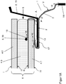
- Figure 1A shows a cross-sectional view of a disc assembly with a flat conductor connection element 1 for an antenna structure 5, wherein the antenna structure 5 is arranged inside a composite disk 4.
- the composite disk 4 comprises two individual disks, namely a rigid first disk 4.1 and a rigid second disk 4.2, which are firmly connected to one another via a thermoplastic adhesive layer 4.3.
- the individual panes have approximately the same size and are made for example of glass, in particular float glass, cast glass and ceramic glass, being equally made of a non-glassy material, such as plastic, in particular polystyrene (PS), polyamide (PA), polyester (PE), polyvinyl chloride (PVC), polycarbonate (PC), polymethylmethacrylate (PMA) or polyethylene terephthalate (PET).
- PS polystyrene
- PA polyamide
- PE polyester
- PVC polyvinyl chloride
- PC polycarbonate
- PMA polymethylmethacrylate
- PET polyethylene terephthalate
- first pane 4.1 and the second pane 4.2 from a flexible and / or a non-transparent material.
- the respective thickness of the first disk 4.1 and the second disk 4.2 may vary widely depending on the use and may for example be in the range of 1 to 24 mm for glass.
- the disc surfaces are denoted by the Roman numerals I-IV, wherein side I V of the outside of the first disc 4.1, side II I the inside of the first disc 4.1, side II of the inside of the second disc 4.2 and side I of the outside second disc 4.2 of the composite disc 4 corresponds.
- side I V of the outside of the first disc 4.1, side II I the inside of the first disc 4.1, side II of the inside of the second disc 4.2 and side I of the outside second disc 4.2 of the composite disc 4 corresponds.
- the side I of the external environment and the side IV of the passenger compartment of the motor vehicle faces.
- the adhesive layer 4.3 for connecting first pane 4.1 and second pane 4.2 preferably contains an adhesive plastic based preferably on polyvinyl butyral (PVB), ethylene-vinyl acetate (EVA) or polyurethane (PU).
- the adhesive layer 4.3 may be formed, for example, as a trilayer. In a trilayer, a film containing, for example, polyethylene terephthalate (PET) is sandwiched between two layers of adhesive plastic.
- PET film can serve as a carrier of a conductive layer and can thus be part of the antenna, in particular of the surface radiator.
- the composite pane 4 is transparent to visible light, for example in the wavelength range from 350 nm to 800 nm, the term "transparency” being understood to mean a light transmission of more than 50%, preferably more than 70% and especially preferably more than 80%.
- the composite pane 4 is glued over a Kleerstrang 13 in a metallic frame 8, such as a vehicle body 19 or vehicle door.
- the composite disk 4 serves, for example, as a windshield of a motor vehicle, but it can also be used elsewhere.
- the second disc 4.2 is provided with an opaque ink layer, which is applied to the side II and forms a frame-shaped circumferential masking strip, which is not shown in more detail in the figures.
- the color layer is preferably made of an electrically non-conductive, black-colored material that can be burned into the first 4.1 or the second disc 4.2.
- the masking strip on the one hand prevents the view of the adhesive strand 13, with which the composite disk 4 is glued into the vehicle body 19, on the other hand it serves as UV protection for the adhesive material used.
- the antenna conductor 5 serves as a line antenna for receiving electromagnetic waves, preferably in the frequency range of the terrestrial Broadcasting bands II to V and is designed for this purpose suitable.
- the antenna conductor 5 is designed in the form of a wire, which is preferably longer than 100 mm and narrower than 1 mm.
- the line conductivity of the antenna conductor 5 is preferably less than 20 ohm / m, more preferably less than 10 ohm / m.
- the length of the antenna conductor 5 is about 650 mm with a width of 0.75 mm. Its line conductivity is, for example, 5 ohms / m.
- the antenna conductor 5 has a sufficient distance to the disc edge 6, whereby a coupling with the vehicle body 19 is counteracted.
- the antenna structure 5 comprises an area antenna.
- the planar antenna contains a transparent conductive coating, which is arranged, for example, on the side III of the second disk 4.2.
- the antenna structure 5 comprises a hybrid antenna structure comprising an area antenna and a line antenna whose signals are conducted to the outside via a common antenna base point 20.
- the transparent, electrically conductive coating perform other functions.
- it may serve as a heat ray-reflecting coating for the purpose of sun protection, thermoregulation or heat insulation or as a heating layer for electrically heating the composite disk 4.
- the antenna structure 5 is connected via its antenna base point 20 to the electrical connection surface 18 of the conductor track 3 of a flat conductor 2.
- the connection between antenna base point 20 and electrical connection surface 18 takes place, for example, by soldering, ultrasonic bonding, gluing or clamping.
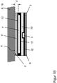
- FIG. 1B shows a cross-sectional view of the flat conductor 2 according to the invention along the section line AA 'from Figure 1A ,
- the flat conductor 2 comprises a base layer 9 which contains a foil of an insulating or dielectric material, preferably a plastic such as polyimide (PI).
- the base layer 9 preferably has a thickness of 10 .mu.m to 500 .mu.m and for example 25 .mu.m.
- the conductor 3 contains a foil of an electrically highly conductive metal, for example copper.
- the thickness of the conductor 3 is from 10 microns to 500 microns and, for example, 35 microns.
- the first dielectric layer 10 includes a sheet of dielectric material, preferably a plastic such as polyimide (PI).
- the first dielectric layer 10 has a thickness of 10 ⁇ m to 2,000 ⁇ m and, for example, 100 ⁇ m.
- the shield 7 contains a foil of an electrically highly conductive metal, for example copper.
- the thickness of the shield 7 is from 10 microns to 500 microns and, for example, 35 microns.
- the conductor 3, the first dielectric layer 10 and the shield 7 form a so-called asymmetric microstrip conductor, in which the signals of the antenna structure 5 are guided in a favorable manner.
- the second dielectric layer 11 contains a foil of a dielectric material, preferably a plastic such as polyimide (PI).
- the second dielectric layer 11 has a thickness of 10 ⁇ m to 500 ⁇ m and for example 25 ⁇ m.
- the base layer 9, the conductor 3, the first dielectric layer 10, the shield 7 and the second dielectric layer 11 are bonded together by suitable adhesive layers 12, for example by an acrylate adhesive.
- the flat conductor 2 extends beyond the edge 6 of the composite disk 4 to the outside.
- the flat conductor 2 is arranged in the region of the surface F adjacent to the vehicle body 19.
- the top V of the flat conductor 2 is the outer side of the second dielectric layer 11.
- the distance d of the shield 7 to the vehicle body 19 is determined by the thickness of the second dielectric layer 11 and the thickness of the Adhesive layer 12 between the shield 7 and second dielectric layer 11 is determined.
- the shield 7, the second dielectric layer 11, the adhesive layer 12 and the vehicle body 19 form a capacitor in the region of the surface F.
- the capacitance C of the capacitor is given by the area F, the thickness of the second dielectric layer 11 and its permittivity, and the thickness of the adhesive layer 12 between the shield 7 and the second dielectric layer 11 and the permittivity of the adhesive layer 12.
- the capacitor becomes the shield 7 capacitively coupled to the vehicle body 19 and thus to the reference ground.
- a high pass is formed, is passed through the electromagnetic interference above the cutoff frequency fG of the high pass to the reference ground.
- the area F at which the shield 7 is at a distance d from the vehicle body 19 is preferably from 30 mm 2 to 200 mm 2 .
- the length of the surface F is, for example, 20 mm.
- the area F is for example 240 mm 2 .
- the distance d corresponds to the thickness of the second dielectric layer 11 and is for example 25 ⁇ m.
- Neglecting the adhesive layer 12 between the shield 7 and the second dielectric layer 11 results in a capacitance C of, for example, 0.3 nF.
- the resistance of the conductor 2 is for example about 2 ohms.
- the upper side V of the flat conductor 2 can be connected to the vehicle body 19 via a further adhesive layer.
- the flat conductor connection element 1, the top V of the flat conductor 2 may be arranged on the vehicle body 19 side facing away.
- the shield 7 is then over the first dielectric layer 10 and the base layer 9 and the between them arranged adhesive layers 12 capacitively coupled to the vehicle body 19.
- FIG. 2 shows a plan view of a flat conductor according to the invention 2.
- the positions of the conductor 3 and the shield 7 in the interior of the flat conductor 2 are shown by dotted lines.
- the flat conductor 2 has an electrical connection surface 18 of the conductor track 3 at one end.
- the flat conductor 2 has a plug 14 at its other end.
- the plug 14 is connected to the conductor track 3.
- the antenna signal to a further connection line, such as a shielded coaxial cable, or be routed directly to the input of a receiving electronics.
- FIG. 3 is a cross-sectional view along the section line BB 'from FIG. 2 shown.
- the flat conductor 2 has a region 16 with a shield 7 and a region 15 without a shield 7.
- FIG. 4 shows a cross-sectional view of the region 16 with shield 7 along the section line DD 'from FIG. 3 and FIG. 5 a cross-sectional view along the section line EE 'from FIG. 3 ,
- the flat conductor 2 In the area 15 without shielding 7, the flat conductor 2 has a smaller thickness and is predominantly arranged inside the composite pane 4.
- the width bL of the wiring 3 is from 0.01 mm to 20 mm and, for example, 0.3 mm.
- the conductor track is arranged in the illustrated embodiment along the center line of the base layer 9.
- the width bA of the shield 7 is from 0.02 mm to 30 mm and, for example, 12 mm.
- the width bA of the shield 7 is preferably larger by a factor of 5 to 30 than the width bL of the printed conductor 3.
- the width of the base layer 9, the first dielectric layer 10 and the second dielectric layer 11 is preferably 0.5 mm to 5 mm wider than the width bA of the shield 7 and is for example 15 mm. Due to the protruding edge, a secure electrical insulation and protection against corrosion of the conductor 3 and the shield 7 is achieved.
- the permittivity of the base layer 9, the first dielectric layer 10, and the second dielectric layer 11 is from 1 to 6, preferably from 3 to 4, and for example, 3.4.
- the permittivity number of the adhesive of the adhesive layers 12 is about 3, for example.
- the widths and thicknesses of the base layer 9, the first dielectric layer 10, and the second dielectric layer 11, the adhesive layers 12, the wiring 3, and the shield 7 are selected so that the line impedance of the film conductor 2 is about 50 ohms.
- the line impedance of the film conductor 2 is thereby adapted to the input impedance of commercially available antenna amplifiers.
- the line impedance of the film conductor 2 is essentially determined by the stationary arrangement of the conductor track 2 and the shield 7. As a result, the flat conductor 2 according to the invention is insensitive to positional tolerances when installed in the vehicle body 19.
- FIG. 6 shows a cross-sectional view of another embodiment of a flat conductor 2 'according to the invention.
- the flat conductor 2 ' is designed in its shielded region 16 as a symmetrical microstrip conductor. To avoid unnecessary repetition, only the differences from the embodiment of FIG. 4 and otherwise reference is made to the statements made there.
- Another shield 7 ' is arranged between the base layer 9 and conductor 3 of the flat conductor 2'.
- a further first dielectric layer 10 ' is arranged between the shield 7' and the conductor track 3.
- the conductor track 3 is shielded both on the underside and on the upper side.
- the shield 7 is capacitively coupled in accordance with the invention via the vehicle body 19 to the reference ground.
- the shield 7 ' is capacitively coupled by the adjacent planar arrangement to the shield 7 with this. As a result of this capacitive coupling, the shield 7 'is also capacitively coupled to the reference ground.
- the shield 7 is galvanically connected to the shield 7'. The galvanic connection takes place for example by a connection of the shields 7 and 7 'in the edge region.
- FIG. 7 shows a flowchart of an embodiment of the method according to the invention.
- FIG. 8 shows the diagram of a comparison measurement between a flat conductor connection element according to the prior art (measurement 1) and a flat conductor connection element 1 according to the invention (measurement 2).
- the antenna structure 5 was a hybrid structure of an area antenna and a line antenna.
- the diagram shows the relative antenna level above the frequency of the radiated high-frequency radiation.
- the high frequency radiation was horizontally polarized.
- the relative antenna level shown in the diagram is an average over the antenna levels of the directional diagram.
- the relative antenna level measured on a flat conductor connection element according to the prior art shows from a frequency of about 600 MHz, a significantly greater attenuation than the relative antenna level measured on a flat conductor connection element according to the invention 1.
- the relative antenna level of a flat conductor Connection element according to the prior art is attenuated by 4 dB compared with a flat conductor connection element 1 according to the invention at a frequency of, for example, 800 MHz.
- the flat conductor connection element 1 according to the invention is therefore more suitable for transmitting high-frequency signals, such as signals for terrestrial television reception, than a flat conductor connection element according to the prior art.
- the flat conductor connection element 1 according to the invention is simple and inexpensive to produce. Since the shield 7 of the flat conductor connection element 1 is capacitively coupled to the reference ground, in addition to the connection of the conductor 3 no further connection technology is necessary. A disc with inventive flat conductor connection element 1 can be easily and quickly installed in a vehicle. Simultaneously line impedance of the flat conductor connection element 1 according to the invention insensitive to positional tolerances when installed in the vehicle body 19th
Description
Die Erfindung betrifft eine Scheibenanordnung mit einem Flachleiter-Anschlusselement für eine Antennenstruktur sowie ein Verfahren zu deren Herstellung.The invention relates to a disk arrangement with a flat conductor connection element for an antenna structure and to a method for the production thereof.
Aktuelle Kraftfahrzeuge benötigen eine Vielzahl von technischen Einrichtungen zum Senden und Empfangen von Grunddiensten wie Rundfunkempfang, vorzugsweise in den Bändern AM, FM oder DAB, Mobiltelefonie in den Bändern GSM 900, GSM 1800 und UMTS sowie satellitengestützer Navigation (GPS).Current motor vehicles require a variety of technical facilities for transmitting and receiving basic services such as radio reception, preferably in the bands AM, FM or DAB, mobile telephony in the bands GSM 900, GSM 1800 and UMTS and satellite-assisted navigation (GPS).
Die in konventionellen Fahrzeugscheiben verbauten Antennen sind vom Typ Linienstrahler. Der Begriff Linienstrahler beschreibt hier eine linienförmige Antenne, die sowohl zum Empfangen als auch zum Senden elektromagnetischer Wellen geeignet ist. Linienstrahler haben eine geometrische Länge, die deren geometrische Breite um mehrere Größenordnungen übersteigt. Die geometrische Länge eines Linienstrahlers ist der Abstand zwischen Antennenfußpunkt und Antennenspitze, die geometrische Breite ist die hierzu senkrechte Abmessung. Für Linienstrahler gilt in der Regel der folgende Zusammenhang: Länge/Breite ≥ 100. Entsprechendes gilt bei Linienstrahlern für deren geometrische Höhe, worunter eine Abmessung zu verstehen ist, die sowohl senkrecht zur Länge als auch senkrecht zur Breite ist, wobei in der Regel der Zusammenhang Länge/Höhe ≥ 100 gilt.The built-in conventional vehicle windscreens antennas are of the type line emitter. The term line emitter here describes a line-shaped antenna which is suitable both for receiving and for transmitting electromagnetic waves. Line radiators have a geometric length that exceeds their geometric width by several orders of magnitude. The geometric length of a line radiator is the distance between antenna base and antenna tip, the geometric width is the vertical dimension. For linear emitters, the following relationship usually applies: length / width ≥ 100. The same applies to line radiators for their geometric height, which is to be understood as meaning a dimension that is both perpendicular to the length and perpendicular to the width, with the context as a rule Length / height ≥ 100 applies.
Linienstrahler dürfen auch in Windschutzscheiben von Kraftfahrzeugen eingesetzt werden, vorausgesetzt, dass sie unter Beachtung gesetzlicher Vorschriften die Sicht des Fahrers nicht beeinträchtigen. Dies kann beispielsweise durch Feindrähte mit einem Durchmesser von typischerweise 10 bis 150 µm erreicht werden. Durch Linienstrahler kann im Bereich der terrestrischen Bänder II bis V ein zufrieden stellendes Antennensignal bereitgestellt werden. Gemäß einer Definition der Internationalen Fernmeldeunion (ITU = International Telecommunication Union) handelt es sich hierbei um den Frequenzbereich von 87,5 MHz bis 960 MHz (Band II: 87,5-100 MHz, Band III: 162-230 MHz, Band IV: 470-582 MHz, Band V: 582-960 MHz). Allerdings lässt sich durch Linienstrahler im vorgelagerten Frequenzbereich von Band I (41-68 MHz) keine zufrieden stellende Empfangsleistung mehr erzielen. Gleiches gilt auch für Frequenzen unterhalb von Band I.Line radiators may also be used in windshields of motor vehicles, provided that they do not impair the driver's visibility in accordance with legal requirements. This can be achieved for example by fine wires with a diameter of typically 10 to 150 microns. By line emitters in the range of the terrestrial bands II to V, a satisfactory antenna signal can be provided. According to a definition of the International Telecommunication Union (ITU = I nternational T elecommunication U nion) is this is the frequency range from 87.5 MHz to 960 MHz (band II: 87.5 to 100 MHz, Volume III: 162-230 MHz, Band IV: 470-582 MHz, Band V: 582-960 MHz). However, line sources in the upstream frequency range of band I can be used (41-68 MHz) can no longer achieve a satisfactory reception performance. The same applies to frequencies below Band I.
Für den Empfang von Frequenzen im Bereich von Band I sind flächenförmige Antennen besser geeignet. Solche flächenförmigen Antennen oder Flächenantennen sind sowohl zum Empfangen als auch zum Senden von elektromagnetischen Wellen geeignet und werden im Folgenden auch als Flächenstrahler bezeichnet.For the reception of frequencies in the range of Band I surface antennas are better suited. Such planar antennas or planar antennas are suitable both for receiving and for transmitting electromagnetic waves and are also referred to below as surface radiators.
Flächenstrahler basieren auf einer flächenhaften, elektrisch leitfähigen, transparenten Beschichtung und sind beispielsweise aus den Druckschriften
Durch eine geeignete Kombination von Linienstrahler und Flächenstrahler können sehr breitbandige Hybridantennen zum Empfangen und Senden elektromagnetischer Wellen in einem Kraftfahrzeug bereitgestellt werden.By means of a suitable combination of line emitters and area radiators, it is possible to provide very broadband hybrid antennas for receiving and transmitting electromagnetic waves in a motor vehicle.
Die Antennensignale werden über einen Anschlussleiter einem Empfangsgerät zugeführt, typischer Weise unter Zwischenschaltung eines Antennenverstärkers. Als Anschlussleiter werden gewöhnlich ungeschirmte Litzendrähte oder Flachleiter eingesetzt. Diese verfügen über einen relativ niedrigen ohmschen Widerstand und verursachen nur geringe ohmsche Leistungsverluste. Solche ungeschirmten Litzendrähte oder Flachleiter lassen keine definierte Signalübertragung zu, da es durch unvermeidliche Lagetoleranzen zu undefinierten Verkopplungen mit der elektrisch leitfähigen Fahrzeugkarosserie oder benachbarten Leitern kommen kann, so dass die Schwankungsbreite wichtiger Antenneneigenschaften wie Bandbreite, Effizienz und Leitungsimpedanz relativ groß ist. Des Weiteren werden über solche ungeschirmten Anschlussleiter leicht elektromagnetische Störungen in das System eingekoppelt und in den Antennenverstärker weitergeleitet.The antenna signals are fed via a connecting conductor to a receiving device, typically with the interposition of an antenna amplifier. As connection conductors usually unshielded stranded wires or flat conductors are used. These have a relatively low ohmic resistance and cause only low ohmic power losses. Such unshielded stranded wires or flat conductors do not allow a defined signal transmission, since unavoidable position tolerances can lead to undefined couplings with the electrically conductive vehicle body or adjacent conductors, so that the fluctuation range of important antenna properties such as bandwidth, efficiency and line impedance is relatively large. Furthermore, such unshielded connection conductors easily coupled electromagnetic interference into the system and forwarded to the antenna amplifier.
Durch die Verwendung spezieller Hochfrequenzleiter, beispielsweise Koaxialleiter, welche neben einem Signalleiter mindestens einen Masseleiter mit sich führen, können Signalverluste vermieden werden. Solche Hochfrequenzleiter sind jedoch aufwändig und kostenintensiv und benötigen relativ viel Bauraum. Zudem erfordern sie eine gleichermaßen aufwändige Verbindungstechnik.By using special high-frequency conductors, such as coaxial, which lead next to a signal conductor at least one ground conductor with it, signal losses can be avoided. However, such high-frequency conductors are complex and expensive and require a relatively large amount of space. In addition, they require an equally complex connection technology.
Demgegenüber besteht die Aufgabe der vorliegenden Erfindung darin, eine Antennenscheibe mit Flachleiter-Anschlusselement mit verbesserter Signalübertragung und geringer Anfälligkeit für Störsignale bereitzustellen. Die Antennenscheibe mit Flachleiter-Anschlusselement soll darüber hinaus einfach und kostengünstig herzustellen sein, über eine einfache Verbindungstechnik verfügen und unempfindlich gegenüber Lagetoleranzen beim Einbau in einen metallischen Rahmen oder eine Fahrzeugkarosserie sein. Diese und weitere Aufgaben werden nach dem Vorschlag der Erfindung durch eine Scheibenanordnung mit einem Flachleiter-Anschlusselement für eine Antennenstruktur mit den Merkmalen des unabhängigen Patentanspruchs gelöst. Vorteilhafte Ausgestaltungen der Erfindung sind durch die Merkmale der Unteransprüche angegeben.In contrast, the object of the present invention is to provide an antenna plate with a flat conductor connection element with improved signal transmission and low susceptibility to spurious signals. The antenna plate with flat conductor connection element should also be simple and inexpensive to manufacture, have a simple connection technology and be insensitive to positional tolerances when installed in a metallic frame or a vehicle body. These and other objects are achieved according to the proposal of the invention by an e disk arrangement with a flat conductor connection element for an antenna structure with the features of the independent claim. Advantageous embodiments of the invention are indicated by the features of the subclaims.
Ein Verfahren zur Herstellung einer Scheibenanordnung mit einem Flachleiter-Anschlusselements und Antennenstruktur sowie die Verwendung einers Scheibenanordnung mit Flachleiter-Anschlusselements und Antennenstruktur gehen aus weiteren unabhängigen Patentansprüchen hervor.A method for producing a r disk assembly having a flat-conductor connecting element and the antenna structure and the use einers disc assembly with flat-conductor connecting element and the antenna structure will be apparent from other independent patent claims.
In Kraftfahrzeugen ist der Antennenverstärker mit der elektrisch leitfähigen Fahrzeugkarosserie elektrisch verbunden, wobei durch diese elektrische Verbindung ein hochfrequenztechnisch wirksames Bezugspotenzial, im Folgenden Bezugsmasse genannt, für das Antennensignal vorgegeben wird. Die nutzbare Antennenspannung ergibt sich aus der Differenz zwischen dem Potenzial des Antennensignals und dem Potenzial der Bezugsmasse.In motor vehicles, the antenna amplifier is electrically connected to the electrically conductive vehicle body, wherein a high-frequency-technically effective reference potential, referred to below as reference ground, for the antenna signal is predetermined by this electrical connection. The usable antenna voltage results from the difference between the potential of the antenna signal and the potential of the reference ground.
Bei dem Flachleiter-Anschlusselement ist eine Antennenstruktur in oder an einer Scheibe angeordnet. Der Flachleiter umfasst:
- eine Grundschicht,
- eine Leiterbahn, die oberhalb der Grundschicht angeordnet ist,
- eine erste dielektrische Schicht, die oberhalb der Leiterbahn angeordnet ist,
- eine Abschirmung, die zumindest abschnittsweise oberhalb der ersten dielektrischen Schicht angeordnet ist und
- eine zweite dielektrische Schicht, die oberhalb der Abschirmung angeordnet ist.
- a base layer,
- a conductor track, which is arranged above the base layer,
- a first dielectric layer disposed above the trace,
- a shield, which is at least partially disposed above the first dielectric layer and
- a second dielectric layer disposed above the shield.
Die Leiterbahn ist über eine Anschlussfläche elektrisch leitend mit der Antennenstruktur verbunden, bevorzugt galvanisch oder kapazitiv. Der Flachleiter verläuft über den Rand der Scheibe nach außen. Außerhalb der Scheibe verläuft der Flachleiter zumindest abschnittsweise benachbart zu einem metallischen Rahmen. Die Abschirmung ist dadurch kapazitiv über den metallischen Rahmen mit einer Bezugsmasse gekoppelt.The conductor track is electrically conductively connected to the antenna structure via a connection surface, preferably galvanically or capacitively. The flat conductor runs over the edge of the disc to the outside. Outside the pane, the flat conductor extends at least partially adjacent to a metallic frame. The shield is thereby capacitively coupled via the metallic frame with a reference ground.
Der Begriff "oberhalb" bezieht sich hier auf die Position in der Schichtenfolge des Flachleiters. Dies bedeutet, der Flachleiter umfasst folgende aufeinander folgende Schichten:
- eine Grundschicht,
- eine Leiterbahn, die auf der Grundschicht angeordnet ist,
- eine erste dielektrische Schicht, die auf der Leiterbahn und falls die Leiterbahn schmäler als die Grundschicht ist, auch auf der freiliegenden Grundschicht angeordnet ist,
- eine Abschirmung, die zumindest abschnittsweise auf der ersten dielektrischen Schicht angeordnet ist und
- eine zweite dielektrische Schicht, die auf der Abschirmung angeordnet ist.
- a base layer,
- a conductor track, which is arranged on the base layer,
- a first dielectric layer disposed on the conductor track and, if the conductor track is narrower than the base layer, also on the exposed base layer,
- a shield, which is at least partially disposed on the first dielectric layer and
- a second dielectric layer disposed on the shield.
Die verschiedenen Schichten des Flachleiters können durch zusätzliche Klebeschichten miteinander verklebt sein.The different layers of the flat conductor can be glued together by additional adhesive layers.
In einer vorteilhaften Ausgestaltung des Flachleiter-Anschlusselements ist die Abschirmung zwischen der Leiterbahn und dem metallischem Rahmen angeordnet. Der metallische Rahmen ist nicht Teil des Flachleiter-Anschlusselements sondern beispielsweise Teil eines Fensterrahmens oder einer Fahrzeugkarosserie. Die Abschirmung, die zweite dielektrische Schicht und ein Teilbereich des metallischen Rahmens bilden eine Kondensatoranordnung, über die die Abschirmung kapazitiv mit dem metallischen Rahmen gekoppelt ist.In an advantageous embodiment of the flat conductor connection element, the shield between the conductor track and the metallic frame is arranged. The metallic frame is not part of the flat conductor connection element but, for example, part of a window frame or a vehicle body. The shield, the second dielectric layer and a portion of the metallic frame form a capacitor arrangement over which the shield is capacitively coupled to the metallic frame.
In einer vorteilhaften Ausgestaltung des Flachleiter-Anschlusselements verläuft die Abschirmung des Flachleiters über mindestens 50%, bevorzugt über mindestens 75% und besonders bevorzugt über mindestens 90% der Fläche des Flachleiters außerhalb der Scheibe. Fläche des Flachleiters bedeutet in diesem Falle die Oberfläche einer flächenhaften Seite des Flachleiters. Die Abschirmung kann zur Verbesserung der Abschirmung auch im Bereich in oder auf der Scheibe angeordnet sein.In an advantageous embodiment of the flat conductor connection element, the shielding of the flat conductor extends over at least 50%, preferably over at least 75% and particularly preferably over at least 90% of the surface of the flat conductor outside the pane. Surface of the flat conductor means in this case the surface of a planar side of the flat conductor. The shield may also be arranged in the region in or on the disk for improving the shielding.
In einer vorteilhaften Ausgestaltung des Flachleiter-Anschlusselements umfasst der metallische Rahmen eine Fahrzeugkarosserie oder einen beweglichen metallischen Rahmen, insbesondere einen metallischen Fensterrahmen. Der metallische Rahmen muss nicht notwendigerweise geschlossen um die äußere Umrandung der Scheibe verlaufen. Ein metallischer Rahmen im Sinne der Erfindung umfasst auch einen metallischen und/oder elektrisch leitfähigen Abschnitt, beispielsweise eine Leiste, einen L-förmigen oder einen U-förmigen Rahmen, der als Bezugsmasse der Antennenstruktur dienen kann.In an advantageous embodiment of the flat conductor connection element, the metallic frame comprises a vehicle body or a movable metallic frame, in particular a metallic window frame. The metallic frame does not necessarily have to be closed around the outer edge of the disc. A metallic frame according to the invention also includes a metallic and / or electrically conductive portion, such as a bar, an L-shaped or a U-shaped frame, which can serve as a reference ground of the antenna structure.
In einer vorteilhaften Ausgestaltung des Flachleiter-Anschlusselements ist die Abschirmung im Bereich einer Fläche von 30 mm2 bis 200 mm2 in einem Abstand von 0,02 mm bis 2 mm zu dem metallischen Rahmen angeordnet. Die Grundschicht, die erste dielektrische Schicht und/oder die zweite dielektrische Schicht haben eine relative Permittivitätszahl von 1 bis 6, bevorzugt von 2 bis 4 und besonders bevorzugt von 3 bis 3,5.In an advantageous embodiment of the flat conductor connecting element, the shield is arranged in the region of an area of 30 mm 2 to 200 mm 2 at a distance of 0.02 mm to 2 mm from the metallic frame. The base layer, the first dielectric layer and / or the second dielectric layer have a relative permittivity of from 1 to 6, preferably from 2 to 4, and more preferably from 3 to 3.5.
Zumindest die Abschirmung, die zweite dielektrische Schicht und der metallische Rahmen bilden einen Kondensator. In einer vorteilhaften Ausgestaltung des Flachleiter-Anschlusselements beträgt die Kapazität des Kondensators von 5 nF bis 10 pF und bevorzugt von 0,1 nF bis 2 nF. Durch den Kondensator wird ein Hochpass gebildet. Über den Hochpass wird elektromagnetische Störstrahlung oberhalb der Grenzfrequenz fG des Hochpasses von der Abschirmung zur Bezugsmasse geleitet.At least the shield, the second dielectric layer and the metallic frame form a capacitor. In an advantageous embodiment of the flat conductor connection element, the capacitance of the capacitor is from 5 nF to 10 pF and preferably from 0.1 nF to 2 nF. Through the capacitor, a high pass is formed. Via the high-pass electromagnetic interference radiation is conducted above the cut-off frequency fG of the high-pass filter from the shield to the reference ground.
In einer vorteilhaften Ausgestaltung des Flachleiter-Anschlusselements beträgt die Grenzfrequenz der Signalübertragung von der Abschirmung zur Bezugsmasse von 20 MHz bis 1000 MHz.In an advantageous embodiment of the flat conductor connection element, the cut-off frequency of the signal transmission from the shield to the reference ground is from 20 MHz to 1000 MHz.
In einer vorteilhaften Ausgestaltung des Flachleiter-Anschlusselements enthält die Grundschicht, die erste dielektrische Schicht und/oder die zweite dielektrische Schicht einen Kunststoff, bevorzugt Polyimid (PI), Polyamid (PA), Polyethylen (PE), Polypropen (PP), Polybutylenterephtalat (PBT), Polycarbonat (PC), Polyethylenenterephtalat (PET), Polyethylennaphtalat (PEN), Polybutadien, Polyvinylchlorid (PVC) oder Polytetrafluorethen (PTFE) sowie Gemische und/oder Copolymere davon. Die Grundschicht, die erste dielektrische Schicht und/oder die zweite dielektrische Schicht können auch eine Lackschicht, bevorzugt Alkydharz, Acrylharz, Epoxidharz oder Polyurethan, oder einen Klebstoff, bevorzugt Acrylatklebstoff, Methylmethacrylatklebstoff, Polyuerthane, Polyolefine, Cyanacrylatklebstoff, Polyepoxide, Silikonkleber und/oder Silanvernetzender-Polymerklebstoff, RTV-Silikonkautschuk, HTV-Silikonkautschuk, peroxidischvernetzter-Silikonkautschuk und/oder additionsvernetzter-Silikonkautschuk sowie Gemische und/oder Copolymere davon, enthalten.In an advantageous embodiment of the flat conductor connection element, the base layer, the first dielectric layer and / or the second dielectric layer contains a plastic, preferably polyimide (PI), polyamide (PA), polyethylene (PE), polypropene (PP), polybutylene terephthalate (PBT ), Polycarbonate (PC), polyethylene terephthalate (PET), polyethylene naphthalate (PEN), polybutadiene, polyvinyl chloride (PVC) or polytetrafluoroethene (PTFE), and mixtures and / or copolymers thereof. The base layer, the first dielectric layer and / or the second dielectric layer can also be a lacquer layer, preferably alkyd resin, acrylic resin, epoxy resin or polyurethane, or an adhesive, preferably acrylate adhesive, methyl methacrylate adhesive, Polyuerthane, polyolefins, cyanoacrylate adhesive, polyepoxides, silicone adhesive and / or Silanvernetzender Polymeric adhesive, RTV silicone rubber, HTV silicone rubber, peroxidischvernetzten silicone rubber and / or addition-crosslinked silicone rubber, and mixtures and / or copolymers thereof.
Die zweite dielektrische Schicht kann auch ein Gas, bevorzugt Luft enthalten, wobei der Abstand zwischen Abschirmung und metallischem Rahmen, beispielsweise durch Abstandshalter gebildet wird.The second dielectric layer can also contain a gas, preferably air, wherein the distance between the shield and the metallic frame, for example formed by spacers.
Des Weiteren kann die zweite dielektrische Schicht durch eine Kunststoffschicht oder eine Lackschicht auf dem metallischen Rahmen gebildet werden, beispielsweise einer Farbschicht auf der Fahrzeugkarosserie.Furthermore, the second dielectric layer can be formed by a plastic layer or a lacquer layer on the metallic frame, for example a color layer on the vehicle body.
In einer vorteilhaften Ausgestaltung des Flachleiter-Anschlusselements enthält die Scheibe eine Einzelscheibe oder ein Verbundscheibe. Die Einzelscheibe oder die einzelnen Scheiben der Verbundscheibe enthalten beispielsweise ein Glas und/oder einen Kunststoff.In an advantageous embodiment of the flat conductor connection element, the disk contains a single disk or a composite disk. The single pane or the individual panes of the composite pane contain, for example, a glass and / or a plastic.
In einer vorteilhaften Ausgestaltung des Flachleiter-Anschlusselements enthält die Leiterbahn und/oder die Abschirmung eine Metallfolie, eine metallisierte Kunststofffolie, eine elektrisch leitfähige Kunststofffolie oder ein Metalldrahtgeflecht. Die Leiterbahn kann auch einen Metalldraht enthalten. Die Leiterbahn und/oder die Abschirmung enthalten bevorzugt ein elektrisch hochleitendes Metall, besonders bevorzugt Kupfer, Aluminium, Zinn, Gold, Silber oder Gemische davon.In an advantageous embodiment of the flat conductor connection element, the conductor track and / or the shield contains a metal foil, a metallized plastic foil, an electrically conductive plastic foil or a metal wire mesh. The track may also contain a metal wire. The conductor track and / or the shield preferably contain an electrically highly conductive metal, particularly preferably copper, aluminum, tin, gold, silver or mixtures thereof.
In einer vorteilhaften Ausgestaltung des Flachleiter-Anschlusselements hat die Abschirmung eine größere Breite als die Breite der Leiterbahn. Das Verhältnis zwischen Breite der Abschirmung und Breite der Leiterbahn bestimmt unter anderem die Impedanz des Flachleiters und beträgt von 2:1 bis 1000:1, bevorzugt von 5:1 bis 30:1 und besonders bevorzugt von 10:1 bis 20:1.In an advantageous embodiment of the flat conductor connecting element, the shield has a greater width than the width of the conductor track. Among other things, the ratio between the width of the shield and the width of the printed conductor determines the impedance of the printed circuit and is from 2: 1 to 1000: 1, preferably from 5: 1 to 30: 1 and particularly preferably from 10: 1 to 20: 1.
In einer vorteilhaften Ausgestaltung des Flachleiter-Anschlusselements umfasst die Antennenstruktur mindestens einen Linienstrahler, einen Flächenstrahler oder eine Hybridstruktur aus Linienstrahler und Flächenstrahler.In an advantageous embodiment of the flat conductor connection element, the antenna structure comprises at least one line emitter, a surface emitter or a hybrid structure of line emitter and surface emitter.
Der Flächenstrahler umfasst zumindest eine elektrisch leitfähige, vorzugsweise transparente Beschichtung, die zumindest eine innenliegende oder außenliegende Seite der Einzelscheibe oder der Verbundscheibe zumindest abschnittsweise bedeckt und zumindest abschnittsweise als flächenförmige Antenne zum Empfangen von elektromagnetischen Wellen dient. Die leitfähige Beschichtung ist zur Verwendung als Flächenantenne geeignet ausgebildet und kann zu diesem Zweck die Scheibe großflächig bedecken. Der Antennenaufbau umfasst weiterhin mindestens eine mit der leitfähigen Beschichtung elektrisch gekoppelte Koppelektrode zum Auskoppeln von Antennensignalen aus der Flächenantenne. Die Koppelelektrode kann beispielsweise kapazitiv oder galvanisch mit der leitfähigen Beschichtung gekoppelt sein.The surface radiator comprises at least one electrically conductive, preferably transparent coating which covers at least one inner or outer side of the single pane or the composite pane at least in sections and at least partially serves as a planar antenna for receiving electromagnetic waves. The conductive coating is suitable for use as a planar antenna and can cover the disc over a large area for this purpose. The antenna structure further comprises at least one coupling electrode electrically coupled to the conductive coating for coupling out antenna signals from the planar antenna. The coupling electrode may, for example, be capacitively or galvanically coupled to the conductive coating.
Der Linienstrahler umfasst zumindest einen linienförmigen Antennenleiter, der beispielsweise in Form eines Drahtes innerhalb einer Verbundscheibe verlegt ist oder aus einer metallischen Druckpaste, beispielsweise im Siebdruckverfahren, auf zumindest eine Seite einer Einzelscheibe oder einer einzelnen Scheibe einer Verbundscheibe gedruckt ist.The line emitter comprises at least one line-shaped antenna conductor, which is laid, for example, in the form of a wire within a composite pane or is printed from a metallic printing paste, for example by screen printing, on at least one side of a single pane or a single pane of a composite pane.
Bei einem hybriden Antennenaufbau werden ein Flächenstrahler und ein Linienstrahler miteinander kombiniert und das Antennensignal vorzugsweise an einem gemeinsamen Antennenfußpunkt bereitgestellt. Zu diesem Zweck sind der Antennenleiter und der gemeinsame Antennenfußpunkt durch einen zweiten Verbindungsleiter miteinander elektrisch leitend verbunden.In a hybrid antenna construction, a surface radiator and a line radiator are combined with each other and the antenna signal is preferably provided at a common antenna base point. For this purpose, the antenna conductor and the common Antennenfußpunkt are electrically connected to each other by a second connection conductor.
Ein weiterer Aspekt umfasst eine Scheibe mit einem Flachleiter-Anschlusselement und einer in oder an der Scheibe angeordneten Antennenstruktur.A further aspect comprises a pane with a flat conductor connection element and an antenna structure arranged in or on the pane.
Ein weiterer Aspekt der Erfindung umfasst ein Verfahren zur Herstellung einer Scheibenanordnung mit einem Flachleiter-Anschlusselements für eine Antennenstruktur, wobei:
- a) eine Leiterbahn eines Flachleiters mit einer Antennenstruktur auf einer ersten Scheibe verbunden wird,
- b) der Flachleiter über einen äußeren Rand der ersten Scheibe herausgeführt wird,
- c) die erste Scheibe in einen metallischen Rahmen eingebaut wird,
- a) a conductor track of a flat conductor is connected to an antenna structure on a first disk,
- b) the lead is led out over an outer edge of the first disc,
- c) the first pane is installed in a metallic frame,
In einer weiteren Ausführungsform des erfindungsgemäßen Verfahrens wird im zweiten Schritt b) der Flachleiter über einen äußeren Rand einer ersten Scheibe herausgeführt und die erste Scheibe über eine thermoplastische Klebeschicht mit einer zweiten Scheibe flächig verbunden.In a further embodiment of the method according to the invention, in the second step b), the flat conductor is brought out via an outer edge of a first pane and the first pane is connected in a planar manner via a thermoplastic adhesive layer to a second pane.
Ein weiterer Aspekt der Erfindung umfasst die Verwendung eine Scheibenanordnung mit einem Flachleiter-Anschlusselement für eine Antennenstruktur in einer Fahrzeugkarosserie oder einer Fahrzeugtür eines Fortbewegungsmittels zu Lande, zu Wasser oder in der Luft, in einem metallischen Rahmen eines Gebäudes, bevorzugt einer Außenfassade oder eines Gebäudefensters oder in einem funktionalen und/oder dekorativen Einzelstück und als Einbauteil in Möbeln und Geräten.Another aspect of the invention comprises the use of a disc arrangement with a flat conductor connection element for an antenna structure in a vehicle body or a vehicle door of a means of transport on land, water or in the air, in a metallic frame of a building, preferably an outer facade or a building window or in a functional and / or decorative single piece and as a built-in part in furniture and appliances.
Es versteht sich, dass die verschiedenen Ausgestaltungen des Antennenaufbaus einzeln oder in beliebigen Kombinationen realisiert sein können. Insbesondere sind die vorstehend genannten und nachstehend zu erläuternden Merkmale nicht nur in den angegebenen Kombinationen, sondern auch in anderen Kombinationen oder in Alleinstellung einsetzbar, ohne den Rahmen der vorliegenden Erfindung zu verlassen.It is understood that the various configurations of the antenna structure can be implemented individually or in any combination. In particular, the features mentioned above and to be explained below can be used not only in the specified combinations but also in other combinations or in isolation, without departing from the scope of the present invention.
Die Erfindung betrifft eine Scheibenanordnung mit Flachleiter-Anschlusselement mit einer Scheibe in einem mit einer Bezugsmasse verbundenen metallischen Rahmen, beispielsweise eine Windschutzscheibe oder Heckscheibe in einer Kraftfahrzeugkarosserie, einer in oder an der Scheibe angeordneten Antennenstruktur und einem mit der Antennenstruktur verbundenen Flachleiter-Anschlusselement.The invention relates to a disc arrangement with a flat conductor connection element with a disc in a metallic frame connected to a reference ground, for example a windshield or rear window in a motor vehicle body, arranged in or on the disc Antenna structure and a connected to the antenna structure flat conductor connection element.
Die erfindungsgemäße Scheibenanordnung mit Flachleiter-Anschlusselement für eine Antennenstruktur umfasst mindestens:
- eine Scheibe, die in einem metallischen Rahmen angeordnet ist,
- eine Antennenstruktur, die in oder an der Scheibe angeordnet ist,
- einen Flachleiter mit
- einer Grundschicht,
- einer Leiterbahn, die oberhalb der Grundschicht angeordnet ist,
- einer ersten dielektrischen Schicht, die oberhalb der Leiterbahn angeordnet ist,
- einer Abschirmung, die zumindest abschnittsweise oberhalb der ersten dielektrischen Schicht angeordnet ist und
- einer zweiten dielektrischen Schicht, die oberhalb der Abschirmung angeordnet ist,
wobei die Leiterbahn mit der Antennenstruktur elektrisch leitend verbunden ist und der Flachleiter über den Rand der Scheibe nach außen verläuft und
der Flachleiter zumindest abschnittsweise benachbart zu dem metallischen Rahmen angeordnet ist und die Abschirmung kapazitiv über den metallischen Rahmen mit der Bezugsmasse gekoppelt ist.
- a disk, which is arranged in a metallic frame,
- an antenna structure disposed in or on the disk,
- a flat conductor with
- a base layer,
- a conductor track, which is arranged above the base layer,
- a first dielectric layer, which is arranged above the conductor track,
- a shield which is arranged at least in sections above the first dielectric layer and
- a second dielectric layer disposed above the shield,
wherein the conductor track is electrically connected to the antenna structure and the flat conductor extends over the edge of the disc to the outside and
the flat conductor is at least partially disposed adjacent to the metallic frame and the shield is capacitively coupled via the metallic frame with the reference ground.
Es versteht sich, dass die Ausgestaltungsmerkmale des Flachleiter-Anschlusselements auch für das Flachleiter-Anschlusselement in der Scheibenanordnung gelten.It is understood that the design features of the flat conductor connection element also apply to the flat conductor connection element in the pane arrangement.
Die Erfindung wird nachfolgend anhand einer Zeichnung und eines Beispiels näher erläutert. Die Zeichnung ist nicht vollständig maßstabsgetreu. Die Erfindung wird durch die Zeichnung in keiner Weise eingeschränkt. Es zeigen:
-
Figur 1A eine Querschnittsdarstellung eines Flachleiter-Anschlusselements für eine Antennenstruktur, -
Figur 1B eine Querschnittdarstellung entlang der Schnittlinie A-A' ausFigur 1A , -
Figur 2 -
Figur 3aus Figur 2 , -
Figur 4aus Figur 3 , -
Figur 5aus Figur 3 , -
Figur 6 -
Figur 7 -
Figur 8 ein Diagramm mit einer Vergleichsmessung.
-
Figure 1A a cross-sectional view of a flat conductor connection element for an antenna structure, -
FIG. 1B a cross-sectional view along the section AA 'fromFigure 1A . -
FIG. 2 a schematic representation of a flat conductor in a plan view, -
FIG. 3 a cross-sectional view along the section line BB 'fromFIG. 2 . -
FIG. 4 a cross-sectional view along the section line DD 'fromFIG. 3 . -
FIG. 5 a cross-sectional view along the section line EE 'fromFIG. 3 . -
FIG. 6 a cross-sectional view of another embodiment of a flat conductor, -
FIG. 7 a flowchart of an embodiment of the method according to the invention and -
FIG. 8 a diagram with a comparison measurement.
Die Verbundscheibe 4 umfasst zwei Einzelscheiben, nämlich eine starre erste Scheibe 4.1 und eine starre zweite Scheibe 4.2, die über eine thermoplastische Klebeschicht 4.3 fest miteinander verbunden sind. Die Einzelscheiben haben in etwa eine gleiche Größe und sind beispielsweise aus Glas, insbesondere Floatglas, Gussglas und Keramikglas gefertigt, wobei sie gleichermaßen aus einem nichtgläsernen Material, beispielsweise Kunststoff, insbesondere Polystyrol (PS), Polyamid (PA), Polyester (PE), Polyvinylchlorid (PVC), Polycarbonat (PC), Polymethylmethacrylat (PMA) oder Polyethylenterephtalat (PET) hergestellt sein können. Allgemein kann jedes Material mit hinreichender Transparenz, ausreichender chemischer Beständigkeit sowie geeigneter Form- und Größenstabilität verwendet werden. Für eine anderweitige Verwendung, beispielsweise als Dekorteil, wäre es auch möglich, die erste Scheibe 4.1 und die zweite Scheibe 4.2 aus einem flexiblen und/oder einem nichttransparenten Material herzustellen. Die jeweilige Dicke der ersten Scheibe 4.1 und der zweiten Scheibe 4.2 kann je nach Verwendung breit variieren und kann für Glas beispielsweise im Bereich von 1 bis 24 mm liegen.The
In üblicher Weise sind die Scheibenflächen mit den römischen Ziffern I-IV bezeichnet, wobei Seite IV der Außenseite der ersten Scheibe 4.1, Seite III der Innenseite der ersten Scheibe 4.1, Seite II der Innenseite der zweiten Scheibe 4.2 und Seite I der Außenseite der zweiten Scheibe 4.2 der Verbundscheibe 4 entspricht. In der Verwendung als Windschutzscheibe ist die Seite I der äußeren Umgebung und die Seite IV der Fahrgastzelle des Kraftfahrzeugs zugewandt.In a conventional manner, the disc surfaces are denoted by the Roman numerals I-IV, wherein side I V of the outside of the first disc 4.1, side II I the inside of the first disc 4.1, side II of the inside of the second disc 4.2 and side I of the outside second disc 4.2 of the
Die Klebeschicht 4.3 zur Verbindung von erster Scheibe 4.1 und zweiter Scheibe 4.2 enthält vorzugsweise einen klebenden Kunststoff bevorzugt auf Basis von Polyvinylbutyral (PVB), Ethylen-Vinyl-Acetat (EVA) oder Polyurethan (PU). Die Klebeschicht 4.3 kann beispielsweise auch als Trilayer ausgebildet sein. Bei einem Trilayer ist eine Folie, die beispielsweise Polyethylenterephtalat (PET) enthält, zwischen zwei Schichten eines klebenden Kunststoffs angeordnet. Die PET-Folie kann als Träger einer leitfähigen Schicht dienen und kann damit Bestandteil der Antenne sein, insbesondere des Flächenstrahlers.The adhesive layer 4.3 for connecting first pane 4.1 and second pane 4.2 preferably contains an adhesive plastic based preferably on polyvinyl butyral (PVB), ethylene-vinyl acetate (EVA) or polyurethane (PU). The adhesive layer 4.3 may be formed, for example, as a trilayer. In a trilayer, a film containing, for example, polyethylene terephthalate (PET) is sandwiched between two layers of adhesive plastic. The PET film can serve as a carrier of a conductive layer and can thus be part of the antenna, in particular of the surface radiator.
Die Verbundscheibe 4 ist für sichtbares Licht beispielsweise im Wellenlängenbereich von 350 nm bis 800 nm transparent, wobei unter dem Begriff "Transparenz" eine Lichtdurchlässigkeit von mehr als 50%, vorzugsweise mehr als 70% und insbesondere bevorzugt mehr als 80% zu verstehen ist.The
Die Verbundscheibe 4 ist über einen Klebestrang 13 in einen metallischen Rahmen 8, beispielsweise eine Fahrzeugkarosserie 19 oder Fahrzeugtür eingeklebt. Die Verbundscheibe 4 dient beispielsweise als Windschutzscheibe eines Kraftfahrzeugs, wobei sie aber auch anderweitig verwendet werden kann.The
Weiterhin ist die zweite Scheibe 4.2 mit einer opaken Farbschicht versehen, die auf der Seite II aufgebracht ist und einen rahmenförmig umlaufenden Maskierungsstreifen bildet, welcher in den Figuren nicht näher dargestellt ist. Die Farbschicht besteht vorzugsweise aus einem elektrisch nicht-leitenden, schwarz eingefärbten Material, das in die erste 4.1 oder die zweite Scheibe 4.2 eingebrannt werden kann. Der Maskierungsstreifen verhindert einerseits die Sicht auf den Klebestrang 13, mit dem die Verbundscheibe 4 in die Fahrzeugkarosserie 19 eingeklebt ist, andererseits dient er als UV-Schutz für das verwendete Klebematerial.Furthermore, the second disc 4.2 is provided with an opaque ink layer, which is applied to the side II and forms a frame-shaped circumferential masking strip, which is not shown in more detail in the figures. The color layer is preferably made of an electrically non-conductive, black-colored material that can be burned into the first 4.1 or the second disc 4.2. The masking strip on the one hand prevents the view of the
Innerhalb einer Randzone der Verbundscheibe 4 befindet sich, eingebettet in die Klebeschicht 4.3, eine Antennenstruktur 5 in Form eines linienförmigen, ungeschirmten Antennenleiters 5. Der Antennenleiter 5 dient als Linienantenne zum Empfangen von elektromagnetischen Wellen, vorzugsweise im Frequenzbereich der terrestrischen Rundfunkbänder II bis V und ist zu diesem Zweck geeignet ausgebildet. Im vorliegenden Ausführungsbeispiel ist der Antennenleiter 5 in Form eines Drahts ausgeführt, der vorzugsweise länger als 100 mm und schmaler als 1 mm ist. Die Linienleitfähigkeit des Antennenleiters 5 ist vorzugsweise geringer als 20 Ohm/m, besonders bevorzugt geringer als 10 Ohm/m. Im gezeigten Ausführungsbeispiel beträgt die Länge des Antennenleiters 5 ca. 650 mm bei einer Breite von 0,75 mm. Seine Linienleitfähigkeit beträgt beispielsweise 5 Ohm/m.Within an edge zone of the
Der Antennenleiter 5 hat einen hinreichenden Abstand zum Scheibenrand 6, wodurch einer Verkopplung mit der Fahrzeugkarosserie 19 entgegen gewirkt wird.The
In einem weiteren Ausführungsbeispiel umfasst die Antennenstruktur 5 eine Flächenantenne. Die Flächenantenne enthält eine transparente leitfähige Beschichtung, die beispielsweise auf der Seite III der zweiten Scheibe 4.2 angeordnet ist. In einem weiteren Ausführungsbeispiel umfasst die Antennenstruktur 5 einen hybriden Antennenaufbau aus einer Flächenantenne und einer Linienantenne, deren Signale über einen gemeinsamen Antennenfußpunkt 20 nach außen geführt werden.In a further embodiment, the
In dem hybriden Antennenaufbau kann die transparente, elektrisch leitfähige Beschichtung, je nach stofflicher Zusammensetzung, weitere Funktionen erfüllen. Beispielsweise kann sie als Wärmestrahlen-reflektierende Beschichtung zum Zwecke eines Sonnenschutzes, Thermoregulierung oder Wärmeisolation oder als Heizschicht zum elektrischen Beheizen der Verbundscheibe 4 dienen. Diese Funktionen sind für die vorliegende Erfindung von untergeordneter Bedeutung.In the hybrid antenna structure, the transparent, electrically conductive coating, depending on the material composition, perform other functions. For example, it may serve as a heat ray-reflecting coating for the purpose of sun protection, thermoregulation or heat insulation or as a heating layer for electrically heating the
Die Antennenstruktur 5 ist über ihren Antennenfußpunkt 20 mit der elektrischen Anschlussfläche 18 der Leiterbahn 3 eines Flachleiters 2 verbunden. Die Verbindung zwischen Antennenfußpunkt 20 und elektrischer Anschlussfläche 18 erfolgt beispielsweise durch Löten, Ultraschallbonden, Kleben oder Klemmen.The
Oberhalb der Grundschicht 9 ist eine Leiterbahn 3 angeordnet. Die Leiterbahn 3 enthält eine Folie eines elektrisch hochleitenden Metalls, beispielsweise Kupfer. Die Dicke der Leiterbahn 3 beträgt von 10 µm bis 500 µm und beispielsweise 35 µm.Above the
Oberhalb der Leiterbahn 3 ist eine erste dielektrische Schicht 10 angeordnet. Die erste dielektrische Schicht 10 enthält eine Folie eines dielektrischen Materials, bevorzugt einen Kunststoff wie Polyimid (PI). Die erste dielektrische Schicht 10 weist eine Dicke von 10 µm bis 2000 µm und beispielsweise 100 µm auf.Above the
Oberhalb der ersten dielektrischen Schicht 10 ist eine Abschirmung 7 angeordnet. Die Abschirmung 7 enthält eine Folie eines elektrisch hochleitenden Metalls, beispielsweise Kupfer. Die Dicke der Abschirmung 7 beträgt von 10 µm bis 500 µm und beispielsweise 35 µm.Above the
Die Leiterbahn 3, die erste dielektrische Schicht 10 und die Abschirmung 7 bilden einen sogenannten asymmetrischen Mikrostreifenleiter, in dem die Signale der Antennenstruktur 5 in günstiger Weise geführt werden.The
Oberhalb der Abschirmung 7 ist eine zweite dielektrische Schicht 11 angeordnet. Die zweite dielektrische Schicht 11 enthält eine Folie eines dielektrischen Materials, bevorzugt einen Kunststoff wie Polyimid (PI). Die zweite dielektrische Schicht 11 weist eine Dicke von 10 µm bis 500 µm und beispielsweise 25 µm auf.Above the
Die Grundschicht 9, die Leiterbahn 3, die erste dielektrische Schicht 10, die Abschirmung 7 und die zweite dielektrische Schicht 11 sind durch geeignete Klebeschichten 12 miteinander verklebt, beispielsweise durch einen Acrylat-Klebstoff.The
Der Flachleiter 2 verläuft über den Rand 6 der Verbundscheibe 4 nach außen. Der Flachleiter 2 ist im Bereich der Fläche F benachbart zur Fahrzeugkarosserie 19 angeordnet. Dabei weist die Oberseite V des Flachleiters 2 zur Fahrzeugkarosserie 19. Die Oberseite V des Flachleiters 2 ist die außenliegende Seite der zweiten dielektrischen Schicht 11. Unterhalb der zweiten dielektrischen Schicht 11 ist die Abschirmung 7 angeordnet. Der Abstand d der Abschirmung 7 zur Fahrzeugkarosserie 19 wird durch die Dicke der zweiten dielektrischen Schicht 11 und die Dicke der Klebeschicht 12 zwischen Abschirmung 7 und zweiter dielektrischen Schicht 11 bestimmt.The
Die Abschirmung 7, die zweite dielektrische Schicht 11, die Klebeschicht 12 und die Fahrzeugkarosserie 19 bilden im Bereich der Fläche F einen Kondensator. Die Kapazität C des Kondensators ergibt sich durch die Fläche F, die Dicke der zweiten dielektrischen Schicht 11 und deren Permittivitätszahl sowie die Dicke der Klebeschicht 12 zwischen Abschirmung 7 und zweiter dielektrischen Schicht 11 und der Permittivitätszahl der Klebeschicht 12. Durch den Kondensator wird die Abschirmung 7 an die Fahrzeugkarosserie 19 und damit an die Bezugsmasse kapazitiv gekoppelt. Durch den Kondensator wird ein Hochpass gebildet, über den elektromagnetische Störstrahlung oberhalb der Grenzfrequenz fG des Hochpasses zur Bezugsmasse geleitet wird.The
Die Fläche F, bei der sich die Abschirmung 7 in einem Abstand d von der Fahrzeugkarosserie19 befindet, beträgt bevorzugt von 30 mm2 bis 200 mm2. Die Breite der Fläche F entspricht beispielsweise einer Breite der Abschirmung 7 von bA = 12 mm. Die Länge der Fläche F beträgt beispielsweise 20 mm. Die Fläche F beträgt beispielsweise 240 mm2. Der Abstand d entspricht der Dicke der zweiten dielektrischen Schicht 11 und beträgt beispielsweise 25 µm. Unter Vernachlässigung der Klebeschicht 12 zwischen Abschirmung 7 und zweiter dielektrischer Schicht 11 ergibt sich eine Kapazität C von beispielsweise 0,3 nF. Der Widerstand der Leiterbahn 2 beträgt beispielsweise etwas 2 Ohm. Die Grenzfrequenz fG des durch den Kondensator gebildeten Hochpass beträgt beispielsweise fG = 1/(2*Pi*R*C) ≈ 275 MHz.The area F at which the
In einer vorteilhaften Ausgestaltung des erfindungsgemäßen Flachleiter-Anschlusselements 1 kann die Oberseite V des Flachleiters 2 über eine weitere Klebeschicht mit der Fahrzeugkarosserie 19 verbunden sein.In an advantageous embodiment of the flat
In einer weiteren vorteilhaften Ausgestaltung erfindungsgemäßen Flachleiter-Anschlusselements 1 kann die Oberseite V des Flachleiters 2 auf der der Fahrzeugkarosserie 19 abgewandten Seite angeordnet sein. Die Abschirmung 7 wird dann über die erste dielektrische Schicht 10 und die Grundschicht 9 sowie den dazwischen angeordneten Klebeschichten 12 mit der Fahrzeugkarosserie 19 kapazitiv gekoppelt.In a further advantageous embodiment of the invention, the flat
In
Die Breite bL der Leiterbahn 3 beträgt von 0,01 mm bis 20 mm und beispielsweise 0,3 mm. Die Leiterbahn ist im dargestellten Ausführungsbeispiel entlang der Mittellinie der Grundschicht 9 angeordnet.The width bL of the
Die Breite bA der Abschirmung 7 beträgt von 0,02 mm bis 30 mm und beispielsweise 12 mm. Die Breite bA der Abschirmung 7 ist bevorzugt um einen Faktor von 5 bis 30 größer als die Breite bL der Leiterbahn 3.The width bA of the
Die Breite der Grundschicht 9, der ersten dielektrischen Schicht 10 und der zweiten dielektrischen Schicht 11 ist bevorzugt um 0,5 mm bis 5 mm breiter als die Breite bA der Abschirmung 7 und beträgt beispielsweise 15 mm. Durch den überstehenden Rand wird eine sichere elektrische Isolation und ein Schutz vor Korrosion der Leiterbahn 3 und der Abschirmung 7 erzielt.The width of the
Die Permittivitätszahl der Grundschicht 9, der ersten dielektrischen Schicht 10 und der zweiten dielektrischen Schicht 11 beträgt von 1 bis 6, bevorzugt von 3 bis 4 und beispielsweise 3,4. Die Permittivitätszahl des Klebers der Klebeschichten 12 beträgt beispielsweise etwa 3.The permittivity of the
Die Breiten und Dicken der Grundschicht 9, der ersten dielektrischen Schicht 10 und der zweiten dielektrischen Schicht 11, der Klebeschichten 12, der Leiterbahn 3 und der Abschirmung 7 sind so gewählt, dass die Leitungsimpedanz des Folienleiters 2 etwa 50 Ohm beträgt. Die Leitungsimpedanz des Folienleiters 2 wird dadurch an die Eingangsimpedanz handelsüblicher Antennenverstärker angepasst.The widths and thicknesses of the
Die Leitungsimpedanz des Folienleiters 2 wird im Wesentlichen durch die zu einander ortsfeste Anordnung von Leiterbahn 2 und Abschirmung 7 bestimmt. Dadurch ist der erfindungsgemäße Flachleiter 2 unempfindlich gegenüber Lagetoleranzen beim Einbau in die Fahrzeugkarosserie 19.The line impedance of the
Der relative Antennenpegel gemessen an einem Flachleiter-Anschlusselement nach dem Stand der Technik (Messung 1), zeigt ab einer Frequenz von etwa 600 MHz eine deutlich größere Abschwächung als der relative Antennenpegel gemessen an einem erfindungsgemäßen Flachleiter-Anschlusselement 1. Der relative Antennenpegel eines Flachleiter-Anschlusselement nach dem Stand der Technik (Messung 1) ist im Vergleich mit einem erfindungsgemäßen Flachleiter-Anschlusselement 1 bei einer Frequenz von beispielsweise 800 MHz um 4 dB abgeschwächt. Das erfindungsgemäße Flachleiter-Anschlusselement 1 ist deshalb besser geeignet hochfrequente Signale, wie Signale für den terrestrischen Fernsehempfang, weiterzuleiten als ein Flachleiter-Anschlusselement nach dem Stand der Technik.The relative antenna level measured on a flat conductor connection element according to the prior art (measurement 1), shows from a frequency of about 600 MHz, a significantly greater attenuation than the relative antenna level measured on a flat conductor connection element according to the
Das erfindungsgemäße Flachleiter-Anschlusselement 1 ist einfach und kostengünstig herzustellen. Da die Abschirmung 7 des Flachleiter-Anschlusselements 1 kapazitiv an die Bezugsmasse angekoppelt ist, ist neben dem Anschluss der Leiterbahn 3 keine weitere Verbindungstechnik notwendig. Eine Scheibe mit erfindungsgemäßem Flachleiter-Anschlusselement 1 kann einfach und schnell in ein Fahrzeug eingebaut werden. Gleichzeitig Leitungsimpedanz des erfindungsgemäßen Flachleiter-Anschlusselements 1 unempfindlich gegenüber Lagetoleranzen beim Einbau in die Fahrzeugkarosserie 19.The flat
Dieses Ergebnis war für den Fachmann unerwartet und überraschend.This result was unexpected and surprising to the skilled person.
- 11
- Scheibe mit Flachleiter-AnschlusselementWasher with flat conductor connection element
- 2, 2'2, 2 '
- Flachleiterflat Head
- 33
- Leiterbahnconductor path
- 44
- Scheibe, VerbundscheibeDisc, composite disc
- 4.14.1
- erste Scheibefirst disc
- 4.24.2
- zweite Scheibesecond disc
- 4.34.3
- thermoplastische Klebeschichtthermoplastic adhesive layer
- 55
- Antennenstrukturantenna structure
- 66
-
Rand der Scheibe 4Edge of the
disc 4 - 7, 7'7, 7 '
- Abschirmungshielding
- 88th
- metallischer Rahmenmetallic frame
- 99
- Grundschichtbase layer
- 10, 10'10, 10 '
- erste dielektrische Schichtfirst dielectric layer
- 1111
- zweite dielektrische Schichtsecond dielectric layer
- 1212
- Klebeschichtadhesive layer
- 1313
- Klebestrang, Klebeverbindung mit Fahrzeugkarosserie 19Adhesive strand, adhesive bond with vehicle body 19
- 1414
- Steckerplug
- 1515
- nicht abgeschirmter Bereichunshielded area
- 1616
- abgeschirmter Bereichshielded area
- 1717
- Fläche der kapazitiven KopplungArea of capacitive coupling
- 1818
-
elektrische Anschlussfläche der Leiterbahn 3electrical connection surface of the
conductor 3 - 1919
- Fahrzeugkarosserievehicle body
- 2020
- Antennenfu ßpunktAntenna footpoint
- A-A'A-A '
- Schnittlinieintersection
- B-B'B-B '
- Schnittlinieintersection
- D-D'D-D '
- Schnittlinieintersection
- E-E'E-E '
- Schnittlinieintersection
- bAbA
-
Breite der Abschirmung 7Width of the
shield 7 - bLbL
-
Breite der Leiterbahn 3Width of the
track 3 - dd
-
Abstand zwischen Abschirmung 7 und metallischem Rahmen 8Distance between
shield 7 and metallic frame 8 - CC
- Kapazitätcapacity
- fGfG
- Grenzfrequenzcut-off frequency
- RR
-
Widerstand der Leiterbahn 2Resistor of the
track 2 - II
-
Außenseite der zweiten Scheibe 4.2, Außenseite der Scheibe 4Outside of the second disk 4.2, outside of the
disk 4 - IIII
- Innenseite der zweiten Scheibe 4.2Inside of the second disc 4.2
- IIIIII
- Innenseite der ersten Scheibe 4.1Inner side of the first disc 4.1
- IVIV
-
Außenseite der ersten Scheibe 4.1, Innenseite der Scheibe 4Outside of the first disc 4.1, inside the
disc 4 - VV
-
Abgeschirmte Seite des Flachleiters 2Shielded side of the
flat conductor 2
Claims (13)
- Pane arrangement, comprising:- a pane (4),- a metallic frame, wherein the pane (4) is arranged in the metallic frame (8) and wherein the metallic frame (8) is connected to a reference ground,- an antenna structure (5), which is arranged in or on the pane (4),- a flat conductor connecting element which is connected to the antenna structure (5) and has a flat conductor (2) with- a base layer (9),- a conductor track (3), which is arranged on the base layer (9),- a first dielectric layer (10), which is arranged on the conductor track (3),- a shield (7), which is arranged, at least in sections, on the first dielectric layer (10), and- a second dielectric layer (11), which is arranged on the shield (7),wherein
the conductor track (3) is electrically conductive connected to the antenna structure (5) and the flat conductor (2) runs outward over the edge (6) of the pane (4), and
the flat conductor (2) is arranged, at least in sections, adjacent the metal frame (8) and the shield (7) is capacitively coupled to the reference ground via the metal frame (8). - Pane arrangement according to claim 1, wherein the shield (7) is arranged between the conductor track (3) and the metal frame (8).
- Pane arrangement according to claim 1 or 2, wherein the shield (7) extends over at least 50%, preferably over at least 75%, and particularly preferably over at least 90% of the surface of the flat conductor (2) outside the pane (4).
- Pane arrangement according to one of claims 1 through 3, wherein the metal frame (8) comprises a vehicle body (19) or a movable metal frame, in particular a metal window frame.
- Pane arrangement according to one of claims 1 through 4, wherein the shield (7) is arranged with an area (F) of 30 mm2 to 200 mm2 at a distance (d) of 0.02 mm to 2 mm from the metal frame (8) and the second dielectric layer (11) has a relative permittivity value of 1 to 6.
- Pane arrangement according to one of claims 1 through 5 wherein the base layer (9), the first dielectric layer (10), and/or the second dielectric layer (9) includes a plastic, preferably polyimide (PI), polyamide (PA), polyethylene (PE), polypropene (PP), polybutylene terephthalate (PBT), polycarbonate (PC), polyethylene terephthalate (PET), polyethylene naphthalate (PEN), polybutadiene, polyvinyl chloride (PVC), or polytetrafluoroethylene (PTFE) as well as mixtures and/or copolymers thereof,
a varnish layer, preferably alkyd resin, acrylic resin, epoxy resin, or polyurethane,
an adhesive, preferably acrylate adhesive, methyl methacrylate adhesive, polyurethanes, polyolefins, cyanoacrylate adhesive, poly epoxies, silicone adhesive, and/or silane crosslinking polymer adhesives, RTV silicone rubber, HTV silicone rubber, peroxide vulcanizing silicone rubber, and/or addition vulcanizing silicone rubber, as well as mixtures and/or copolymers thereof,
or a gas, preferably air. - Pane arrangement according to one of claims 1 through 6, wherein the conductor track (3) and/or the shield (7) includes a metal foil, a metallized polymer film, a metal wire, or a metal wire mesh.
- Pane arrangement according to one of claims 1 through 7, wherein the conductor track (3) and/or the shield (7) includes copper, aluminum, tin, gold, silver, or mixtures thereof.
- Pane arrangement according to one of claims 1 through 8, wherein the shield (7) includes a metal foil and the metal foil has a width (bA) greater than the width (bL) of the conductor track (3).
- Pane arrangement according to one of claims 1 through 9, wherein the antenna structure (5) comprises at least one linear emitter, one planar emitter, or a hybrid structure made of linear emitters and planar emitters.
- Method for producing a pane arrangement according to one of claims 1 through 10, wherein:a) a conductor track (3) of a flat conductor (2) is connected to an antenna structure (5) on a first pane (4.1),b) the flat conductor (2) is led out over an outer edge (6) of the first pane (4.1),c) the first pane (4.1) is installed in a metal frame (8),wherein a shield (7) of the flat conductor (2) is arranged over at least one second dielectric layer (11) adjacent, at least in sections, to the metal frame and the shield (7) is capacitively coupled to a reference ground via the metal frame (8).
- Method for producing a pane arrangement according to claim 11, wherein in step b) the flat conductor (2) is led out over an outer edge (6) of a first pane (4.1), and the first pane (4.1) is connected surface-to-surface to a second pane (4.2) via a thermoplastic adhesive layer (4.3).
- Use of a pane arrangement according to one of claims 1 through 10 for an antenna structure (5), which is arranged on a single pane or in or on a composite glass pane, in a vehicle body (19) or a vehicle door of a means of transportation on land, on water, or in the air, in a metal frame of a building, preferably an exterior façade or a building window, or in a functional and/or decorative individual piece and as a built-in part in furniture and devices.
Priority Applications (2)
| Application Number | Priority Date | Filing Date | Title |
|---|---|---|---|
| PL12706820T PL2695233T3 (en) | 2011-04-06 | 2012-02-27 | Flat-conductor connection element for an antenna structure |
| EP12706820.3A EP2695233B1 (en) | 2011-04-06 | 2012-02-27 | Flat-conductor connection element for an antenna structure |
Applications Claiming Priority (3)
| Application Number | Priority Date | Filing Date | Title |
|---|---|---|---|
| EP11161283 | 2011-04-06 | ||
| PCT/EP2012/053245 WO2012136411A1 (en) | 2011-04-06 | 2012-02-27 | Flat-conductor connection element for an antenna structure |
| EP12706820.3A EP2695233B1 (en) | 2011-04-06 | 2012-02-27 | Flat-conductor connection element for an antenna structure |
Publications (2)
| Publication Number | Publication Date |
|---|---|
| EP2695233A1 EP2695233A1 (en) | 2014-02-12 |
| EP2695233B1 true EP2695233B1 (en) | 2018-10-24 |
Family
ID=44513430
Family Applications (1)
| Application Number | Title | Priority Date | Filing Date |
|---|---|---|---|
| EP12706820.3A Active EP2695233B1 (en) | 2011-04-06 | 2012-02-27 | Flat-conductor connection element for an antenna structure |
Country Status (13)
| Country | Link |
|---|---|
| US (1) | US9171658B2 (en) |
| EP (1) | EP2695233B1 (en) |
| JP (1) | JP5805299B2 (en) |
| KR (1) | KR101571948B1 (en) |
| CN (1) | CN103636060B (en) |
| BR (1) | BR112013024505B1 (en) |
| EA (1) | EA026715B1 (en) |
| ES (1) | ES2707608T3 (en) |
| MX (1) | MX2013011486A (en) |
| PL (1) | PL2695233T3 (en) |
| PT (1) | PT2695233T (en) |
| TR (1) | TR201900175T4 (en) |
| WO (1) | WO2012136411A1 (en) |
Cited By (2)
| Publication number | Priority date | Publication date | Assignee | Title |
|---|---|---|---|---|
| WO2024002685A1 (en) * | 2022-06-28 | 2024-01-04 | Saint-Gobain Glass France | Ribbon cable, electrical connecting line, substrate, and composite pane |
| WO2024012857A1 (en) | 2022-07-14 | 2024-01-18 | Saint-Gobain Glass France | Ribbon cable with temperature sensor, connection arrangement, and method |
Families Citing this family (27)
| Publication number | Priority date | Publication date | Assignee | Title |
|---|---|---|---|---|
| JP6171876B2 (en) * | 2012-11-14 | 2017-08-02 | 旭硝子株式会社 | FEEDING STRUCTURE AND WINDOW RESIN PLATE FORM WITH THE SAME, AND METHOD FOR MANUFACTURING WINDOW RESIN PLATE FORM WITH FEEDING STRUCTURE |
| EP3059801B1 (en) | 2013-10-16 | 2019-04-24 | AGC Inc. | Electricity-supplying structure, resin plate for window provided with said structure, and method for manufacturing resin plate for window provided with electricity-supplying structure |
| US20170033433A1 (en) * | 2014-04-14 | 2017-02-02 | Shanghai Amphenol Airwave Communication Electronics Co., Ltd. | Windshield Antenna |
| DE102014016564A1 (en) * | 2014-11-08 | 2016-05-12 | GM Global Technology Operations LLC (n. d. Ges. d. Staates Delaware) | Disc arrangement for a motor vehicle |
| WO2016096432A1 (en) | 2014-12-16 | 2016-06-23 | Saint-Gobain Glass France | Electrically heatable windscreen antenna, and method for producing same |
| CN107108353B (en) * | 2014-12-24 | 2020-03-17 | Agc株式会社 | Electrical connection member and laminated plate using same |
| CN106463813A (en) | 2015-04-08 | 2017-02-22 | 法国圣戈班玻璃厂 | Vehicle window aerial pane |
| CN106463812A (en) | 2015-04-08 | 2017-02-22 | 法国圣戈班玻璃厂 | Windscreen antenna |
| DE102015214377A1 (en) * | 2015-07-29 | 2017-02-02 | Brose Fahrzeugteile Gmbh & Co. Kommanditgesellschaft, Bamberg | Device for fastening and electrical contacting of a vehicle window pane |
| DE102015220115B4 (en) * | 2015-10-15 | 2019-11-07 | Lisa Dräxlmaier GmbH | ELECTRICAL ENERGY SUPPLY SYSTEM AND MANUFACTURING METHOD FOR SUCH A |
| JP2017149380A (en) * | 2016-02-26 | 2017-08-31 | イビデン株式会社 | Resin rear window and resin window |
| GB201608383D0 (en) | 2016-05-12 | 2016-06-29 | Pilkington Group Ltd | Connector for antennas, a glazing comprising the connector and an antenna system comprising the connector |
| JP6894212B2 (en) * | 2016-11-08 | 2021-06-30 | 矢崎総業株式会社 | Planar antenna body |
| CN106602271B (en) * | 2017-02-20 | 2024-02-02 | 长城信息股份有限公司 | Structure-enhanced antenna |
| CN107945934A (en) * | 2017-10-17 | 2018-04-20 | 安徽庆华电缆有限公司 | A kind of thermoplastic elastomer (TPE) insulating sheath flexible cable |
| JP6914809B2 (en) * | 2017-11-07 | 2021-08-04 | Agc株式会社 | Windshield for vehicles |
| US10910692B2 (en) * | 2017-11-28 | 2021-02-02 | Taoglas Group Holdings Limited | In-glass high performance antenna |
| JP7140825B2 (en) * | 2018-03-16 | 2022-09-21 | Agc株式会社 | Antenna unit, window glass with antenna unit and matching body |
| RU2768346C1 (en) * | 2018-03-27 | 2022-03-23 | ЭйДжиСи Инк. | Glass structure and its production method |
| RU2756295C1 (en) * | 2018-06-26 | 2021-09-29 | Сэн-Гобэн Гласс Франс | Panel with electrical connection element and connecting cable |
| US11108141B2 (en) | 2018-09-12 | 2021-08-31 | Taoglas Group Holdings Limited | Embedded patch antennas, systems and methods |
| CN111989821A (en) * | 2019-03-21 | 2020-11-24 | 法国圣戈班玻璃厂 | Vehicle glazing |
| MA55870A (en) | 2019-05-08 | 2022-03-16 | Saint Gobain | VEHICLE GLASS |
| US11783156B2 (en) * | 2019-08-09 | 2023-10-10 | Saint-Gobain Glass France | Glazing with RFID transponder |
| CN113365814A (en) | 2020-01-06 | 2021-09-07 | 法国圣戈班玻璃厂 | Vehicle glazing with capacitive sensor electrodes |
| DE102020207429A1 (en) | 2020-06-16 | 2021-12-16 | Volkswagen Aktiengesellschaft | Energy supply with strain relief for a functionalized pane composite |
| CN116547767A (en) | 2021-09-29 | 2023-08-04 | 法国圣戈班玻璃厂 | Flat belt cable for fracture identification, coupling assembly with composite disc, method for fracture identification and use of flat belt cable |
Family Cites Families (20)
| Publication number | Priority date | Publication date | Assignee | Title |
|---|---|---|---|---|
| US3459879A (en) | 1967-05-29 | 1969-08-05 | Hughes Aircraft Co | Flexible multiflat conductor characteristic impedance cable |
| US5867238A (en) | 1991-01-11 | 1999-02-02 | Minnesota Mining And Manufacturing Company | Polymer-dispersed liquid crystal device having an ultraviolet-polymerizable matrix and a variable optical transmission and a method for preparing same |
| JPH07122920A (en) * | 1993-10-21 | 1995-05-12 | Nippon Sheet Glass Co Ltd | Grounding structure of film antenna for vehicle |
| US5670966A (en) | 1994-12-27 | 1997-09-23 | Ppg Industries, Inc. | Glass antenna for vehicle window |
| DE19536131C2 (en) | 1995-09-28 | 2002-05-02 | Saint Gobain Sekurit D Gmbh | Diversity antenna disc for vehicles with connection elements |
| DE19735395A1 (en) | 1996-08-16 | 1998-02-19 | Lindenmeier Heinz | Low loss aerial especially for vehicle windscreen |
| DE19832228C2 (en) | 1998-07-17 | 2002-05-08 | Saint Gobain Sekurit D Gmbh | Antenna disc for motor vehicles |
| WO2001082410A1 (en) | 2000-04-19 | 2001-11-01 | Advanced Automotive Antennas, S.L. | Multilevel advanced antenna for motor vehicles |
| DE10106125B4 (en) | 2001-02-08 | 2014-04-10 | Delphi Technologies, Inc. | Vehicle window with antenna structures |
| JP2003101319A (en) * | 2001-09-26 | 2003-04-04 | Toshiba Corp | On-vehicle antenna and its high-frequency transmission line |
| DE20210286U1 (en) | 2002-07-03 | 2002-12-12 | Fuba Automotive Gmbh | Adapter for HF connections |
| DE10301352B3 (en) | 2003-01-16 | 2004-07-15 | Saint-Gobain Sekurit Deutschland Gmbh & Co. Kg | Solder terminal element for connecting electrical conductor with conductor structure applied to substrate e.g. automobile windscreen |
| DE10319606B4 (en) | 2003-05-02 | 2005-07-14 | Saint-Gobain Sekurit Deutschland Gmbh & Co. Kg | Antenna disc for vehicles |
| DE10351488A1 (en) | 2003-11-04 | 2005-06-16 | Saint-Gobain Sekurit Deutschland Gmbh & Co. Kg | Antenna arrangement for sending and receiving electromagnetic signals comprises a flat support substrate made from a dielectric material, and strip conductors formed on both surfaces of the substrate |
| DE102004056866A1 (en) | 2004-11-25 | 2006-01-26 | Leoni Bordnetz-Systeme Gmbh & Co Kg | Extruded flat cable has at least one screened conducting track embedded in insulating material, enclosed by shield, earth conductor that contacts shielding with at least one of its long sides, common casing |
| DE202004019286U1 (en) * | 2004-12-14 | 2006-04-20 | Saint-Gobain Sekurit Deutschland Gmbh & Co. Kg | Flat, electrically conductive connector element for window panes incorporates a local wear resistant reinforcement which consists of a material capable of self-healing of surface damage |
| FR2913141A3 (en) | 2007-02-27 | 2008-08-29 | Renault Sas | Flat flexible cable for e.g. midair type windscreen, of motor vehicle, has adhesive layer covering surface of band opposed to conductors to allow direct bonding of cable on glass surface, where cable has specific thickness |
| GB0714723D0 (en) | 2007-07-30 | 2007-09-12 | Pilkington Automotive D Gmbh | Improved electrical connector |
| JP4603617B2 (en) * | 2008-11-27 | 2010-12-22 | 京セラ株式会社 | Communication equipment |
| JP2012151829A (en) * | 2010-12-27 | 2012-08-09 | Canon Components Inc | Flexible printed wiring board and radio communication module |
-
2012
- 2012-02-27 PT PT12706820T patent/PT2695233T/en unknown
- 2012-02-27 EA EA201391477A patent/EA026715B1/en not_active IP Right Cessation
- 2012-02-27 PL PL12706820T patent/PL2695233T3/en unknown
- 2012-02-27 CN CN201280017167.8A patent/CN103636060B/en active Active
- 2012-02-27 US US14/110,124 patent/US9171658B2/en not_active Expired - Fee Related
- 2012-02-27 ES ES12706820T patent/ES2707608T3/en active Active
- 2012-02-27 KR KR1020137029026A patent/KR101571948B1/en active IP Right Grant
- 2012-02-27 TR TR2019/00175T patent/TR201900175T4/en unknown
- 2012-02-27 MX MX2013011486A patent/MX2013011486A/en active IP Right Grant
- 2012-02-27 JP JP2014503042A patent/JP5805299B2/en not_active Expired - Fee Related
- 2012-02-27 BR BR112013024505-0A patent/BR112013024505B1/en not_active IP Right Cessation
- 2012-02-27 WO PCT/EP2012/053245 patent/WO2012136411A1/en active Application Filing
- 2012-02-27 EP EP12706820.3A patent/EP2695233B1/en active Active
Non-Patent Citations (1)
| Title |
|---|
| None * |
Cited By (2)
| Publication number | Priority date | Publication date | Assignee | Title |
|---|---|---|---|---|
| WO2024002685A1 (en) * | 2022-06-28 | 2024-01-04 | Saint-Gobain Glass France | Ribbon cable, electrical connecting line, substrate, and composite pane |
| WO2024012857A1 (en) | 2022-07-14 | 2024-01-18 | Saint-Gobain Glass France | Ribbon cable with temperature sensor, connection arrangement, and method |
Also Published As
| Publication number | Publication date |
|---|---|
| MX2013011486A (en) | 2013-11-04 |
| CN103636060A (en) | 2014-03-12 |
| EA201391477A1 (en) | 2014-11-28 |
| JP2014514836A (en) | 2014-06-19 |
| PL2695233T3 (en) | 2019-05-31 |
| ES2707608T3 (en) | 2019-04-04 |
| US20140060921A1 (en) | 2014-03-06 |
| KR20140025428A (en) | 2014-03-04 |
| EA026715B1 (en) | 2017-05-31 |
| TR201900175T4 (en) | 2019-02-21 |
| PT2695233T (en) | 2019-01-30 |
| BR112013024505B1 (en) | 2022-01-25 |
| EP2695233A1 (en) | 2014-02-12 |
| WO2012136411A1 (en) | 2012-10-11 |
| CN103636060B (en) | 2016-03-23 |
| US9171658B2 (en) | 2015-10-27 |
| KR101571948B1 (en) | 2015-11-25 |
| BR112013024505A2 (en) | 2016-12-27 |
| JP5805299B2 (en) | 2015-11-04 |
Similar Documents
| Publication | Publication Date | Title |
|---|---|---|
| EP2695233B1 (en) | Flat-conductor connection element for an antenna structure | |
| EP3235339B1 (en) | Electrically heatable antenna disc and method for producing same | |
| EP3281247B1 (en) | Vehicle antenna window | |
| EP2580807B1 (en) | Antenna structure with improved signal/noise ratio | |
| EP3281248B1 (en) | Antenna disc | |
| EP2936926B1 (en) | Glasspane with electrical heating layer | |
| EP2465164B1 (en) | Panel having electrically conductive structures | |
| DE102017109746A1 (en) | FLEXIBLE DUAL-BAND ANTENNA WITH SEGMENTED SURFACE TREATMENT | |
| EP3189706B1 (en) | Pane with electric heating area | |
| EP2572403B1 (en) | Antenna with optimised bandwidth with optimised construction of surface and line transmitter | |
| DE112014006587T5 (en) | Windshield antenna | |
| WO2018215317A1 (en) | Pane arrangement with electrical connector | |
| EP3847581B1 (en) | Vehicle pane with transponder | |
| WO2020201170A1 (en) | Windscreen antenna | |
| DE112021003477T5 (en) | WINDOW GLASS FOR A VEHICLE AND VEHICLE STRUCTURE | |
| DE202018006266U1 (en) | Vehicle window with a transponder | |
| DE202020005661U1 (en) | Antenna disk with antenna of planar design | |
| DE102019110791A1 (en) | TRANSPARENT DISC ASSEMBLY WITH INTEGRATED ANTENNA | |
| WO2021110714A1 (en) | Vehicle pane | |
| WO2020182563A1 (en) | Antenna arrangement for a vehicle | |
| WO2021110713A1 (en) | Vehicle pane | |
| WO2011141151A2 (en) | Antennas in metallised window panes of a vehicle |
Legal Events
| Date | Code | Title | Description |
|---|---|---|---|
| PUAI | Public reference made under article 153(3) epc to a published international application that has entered the european phase |
Free format text: ORIGINAL CODE: 0009012 |
|
| 17P | Request for examination filed |
Effective date: 20131007 |
|
| AK | Designated contracting states |
Kind code of ref document: A1 Designated state(s): AL AT BE BG CH CY CZ DE DK EE ES FI FR GB GR HR HU IE IS IT LI LT LU LV MC MK MT NL NO PL PT RO RS SE SI SK SM TR |
|
| RIN1 | Information on inventor provided before grant (corrected) |
Inventor name: DEGEN, CHRISTOPH Inventor name: DROSTE, STEFAN Inventor name: REUL, BERNHARD |
|
| DAX | Request for extension of the european patent (deleted) | ||
| GRAP | Despatch of communication of intention to grant a patent |
Free format text: ORIGINAL CODE: EPIDOSNIGR1 |
|
| STAA | Information on the status of an ep patent application or granted ep patent |
Free format text: STATUS: GRANT OF PATENT IS INTENDED |
|
| INTG | Intention to grant announced |
Effective date: 20180502 |
|
| GRAS | Grant fee paid |
Free format text: ORIGINAL CODE: EPIDOSNIGR3 |
|
| GRAA | (expected) grant |
Free format text: ORIGINAL CODE: 0009210 |
|
| STAA | Information on the status of an ep patent application or granted ep patent |
Free format text: STATUS: THE PATENT HAS BEEN GRANTED |
|
| AK | Designated contracting states |
Kind code of ref document: B1 Designated state(s): AL AT BE BG CH CY CZ DE DK EE ES FI FR GB GR HR HU IE IS IT LI LT LU LV MC MK MT NL NO PL PT RO RS SE SI SK SM TR |
|
| REG | Reference to a national code |
Ref country code: GB Ref legal event code: FG4D Free format text: NOT ENGLISH |
|
| REG | Reference to a national code |
Ref country code: CH Ref legal event code: EP |
|
| REG | Reference to a national code |
Ref country code: IE Ref legal event code: FG4D Free format text: LANGUAGE OF EP DOCUMENT: GERMAN |
|
| REG | Reference to a national code |
Ref country code: AT Ref legal event code: REF Ref document number: 1057782 Country of ref document: AT Kind code of ref document: T Effective date: 20181115 |
|
| REG | Reference to a national code |
Ref country code: DE Ref legal event code: R096 Ref document number: 502012013674 Country of ref document: DE |
|
| REG | Reference to a national code |
Ref country code: RO Ref legal event code: EPE |
|
| REG | Reference to a national code |
Ref country code: PT Ref legal event code: SC4A Ref document number: 2695233 Country of ref document: PT Date of ref document: 20190130 Kind code of ref document: T Free format text: AVAILABILITY OF NATIONAL TRANSLATION Effective date: 20190121 Ref country code: NL Ref legal event code: FP |
|
| REG | Reference to a national code |
Ref country code: SE Ref legal event code: TRGR |
|
| REG | Reference to a national code |
Ref country code: LT Ref legal event code: MG4D |
|
| REG | Reference to a national code |
Ref country code: ES Ref legal event code: FG2A Ref document number: 2707608 Country of ref document: ES Kind code of ref document: T3 Effective date: 20190404 |
|
| PG25 | Lapsed in a contracting state [announced via postgrant information from national office to epo] |
Ref country code: FI Free format text: LAPSE BECAUSE OF FAILURE TO SUBMIT A TRANSLATION OF THE DESCRIPTION OR TO PAY THE FEE WITHIN THE PRESCRIBED TIME-LIMIT Effective date: 20181024 Ref country code: LV Free format text: LAPSE BECAUSE OF FAILURE TO SUBMIT A TRANSLATION OF THE DESCRIPTION OR TO PAY THE FEE WITHIN THE PRESCRIBED TIME-LIMIT Effective date: 20181024 Ref country code: IS Free format text: LAPSE BECAUSE OF FAILURE TO SUBMIT A TRANSLATION OF THE DESCRIPTION OR TO PAY THE FEE WITHIN THE PRESCRIBED TIME-LIMIT Effective date: 20190224 Ref country code: NO Free format text: LAPSE BECAUSE OF FAILURE TO SUBMIT A TRANSLATION OF THE DESCRIPTION OR TO PAY THE FEE WITHIN THE PRESCRIBED TIME-LIMIT Effective date: 20190124 Ref country code: BG Free format text: LAPSE BECAUSE OF FAILURE TO SUBMIT A TRANSLATION OF THE DESCRIPTION OR TO PAY THE FEE WITHIN THE PRESCRIBED TIME-LIMIT Effective date: 20190124 Ref country code: HR Free format text: LAPSE BECAUSE OF FAILURE TO SUBMIT A TRANSLATION OF THE DESCRIPTION OR TO PAY THE FEE WITHIN THE PRESCRIBED TIME-LIMIT Effective date: 20181024 Ref country code: LT Free format text: LAPSE BECAUSE OF FAILURE TO SUBMIT A TRANSLATION OF THE DESCRIPTION OR TO PAY THE FEE WITHIN THE PRESCRIBED TIME-LIMIT Effective date: 20181024 |
|
| PG25 | Lapsed in a contracting state [announced via postgrant information from national office to epo] |
Ref country code: GR Free format text: LAPSE BECAUSE OF FAILURE TO SUBMIT A TRANSLATION OF THE DESCRIPTION OR TO PAY THE FEE WITHIN THE PRESCRIBED TIME-LIMIT Effective date: 20190125 Ref country code: RS Free format text: LAPSE BECAUSE OF FAILURE TO SUBMIT A TRANSLATION OF THE DESCRIPTION OR TO PAY THE FEE WITHIN THE PRESCRIBED TIME-LIMIT Effective date: 20181024 Ref country code: AL Free format text: LAPSE BECAUSE OF FAILURE TO SUBMIT A TRANSLATION OF THE DESCRIPTION OR TO PAY THE FEE WITHIN THE PRESCRIBED TIME-LIMIT Effective date: 20181024 |
|
| REG | Reference to a national code |
Ref country code: SK Ref legal event code: T3 Ref document number: E 29904 Country of ref document: SK |
|
| REG | Reference to a national code |
Ref country code: DE Ref legal event code: R097 Ref document number: 502012013674 Country of ref document: DE |
|
| PG25 | Lapsed in a contracting state [announced via postgrant information from national office to epo] |
Ref country code: DK Free format text: LAPSE BECAUSE OF FAILURE TO SUBMIT A TRANSLATION OF THE DESCRIPTION OR TO PAY THE FEE WITHIN THE PRESCRIBED TIME-LIMIT Effective date: 20181024 |
|
| PG25 | Lapsed in a contracting state [announced via postgrant information from national office to epo] |
Ref country code: SM Free format text: LAPSE BECAUSE OF FAILURE TO SUBMIT A TRANSLATION OF THE DESCRIPTION OR TO PAY THE FEE WITHIN THE PRESCRIBED TIME-LIMIT Effective date: 20181024 Ref country code: EE Free format text: LAPSE BECAUSE OF FAILURE TO SUBMIT A TRANSLATION OF THE DESCRIPTION OR TO PAY THE FEE WITHIN THE PRESCRIBED TIME-LIMIT Effective date: 20181024 |
|
| PLBE | No opposition filed within time limit |
Free format text: ORIGINAL CODE: 0009261 |
|
| STAA | Information on the status of an ep patent application or granted ep patent |
Free format text: STATUS: NO OPPOSITION FILED WITHIN TIME LIMIT |
|
| REG | Reference to a national code |
Ref country code: CH Ref legal event code: PL |
|
| 26N | No opposition filed |
Effective date: 20190725 |
|
| PG25 | Lapsed in a contracting state [announced via postgrant information from national office to epo] |
Ref country code: SI Free format text: LAPSE BECAUSE OF FAILURE TO SUBMIT A TRANSLATION OF THE DESCRIPTION OR TO PAY THE FEE WITHIN THE PRESCRIBED TIME-LIMIT Effective date: 20181024 Ref country code: MC Free format text: LAPSE BECAUSE OF FAILURE TO SUBMIT A TRANSLATION OF THE DESCRIPTION OR TO PAY THE FEE WITHIN THE PRESCRIBED TIME-LIMIT Effective date: 20181024 |
|
| REG | Reference to a national code |
Ref country code: IE Ref legal event code: MM4A |
|
| PG25 | Lapsed in a contracting state [announced via postgrant information from national office to epo] |
Ref country code: LI Free format text: LAPSE BECAUSE OF NON-PAYMENT OF DUE FEES Effective date: 20190228 Ref country code: CH Free format text: LAPSE BECAUSE OF NON-PAYMENT OF DUE FEES Effective date: 20190228 |
|
| PG25 | Lapsed in a contracting state [announced via postgrant information from national office to epo] |
Ref country code: IE Free format text: LAPSE BECAUSE OF NON-PAYMENT OF DUE FEES Effective date: 20190227 |
|
| REG | Reference to a national code |
Ref country code: AT Ref legal event code: MM01 Ref document number: 1057782 Country of ref document: AT Kind code of ref document: T Effective date: 20190227 |
|
| PG25 | Lapsed in a contracting state [announced via postgrant information from national office to epo] |
Ref country code: AT Free format text: LAPSE BECAUSE OF NON-PAYMENT OF DUE FEES Effective date: 20190227 |
|
| PGFP | Annual fee paid to national office [announced via postgrant information from national office to epo] |
Ref country code: PT Payment date: 20200227 Year of fee payment: 9 Ref country code: SE Payment date: 20200210 Year of fee payment: 9 |
|
| PG25 | Lapsed in a contracting state [announced via postgrant information from national office to epo] |
Ref country code: MT Free format text: LAPSE BECAUSE OF FAILURE TO SUBMIT A TRANSLATION OF THE DESCRIPTION OR TO PAY THE FEE WITHIN THE PRESCRIBED TIME-LIMIT Effective date: 20181024 |
|
| PG25 | Lapsed in a contracting state [announced via postgrant information from national office to epo] |
Ref country code: CY Free format text: LAPSE BECAUSE OF FAILURE TO SUBMIT A TRANSLATION OF THE DESCRIPTION OR TO PAY THE FEE WITHIN THE PRESCRIBED TIME-LIMIT Effective date: 20181024 |
|
| PG25 | Lapsed in a contracting state [announced via postgrant information from national office to epo] |
Ref country code: HU Free format text: LAPSE BECAUSE OF FAILURE TO SUBMIT A TRANSLATION OF THE DESCRIPTION OR TO PAY THE FEE WITHIN THE PRESCRIBED TIME-LIMIT; INVALID AB INITIO Effective date: 20120227 |
|
| REG | Reference to a national code |
Ref country code: SE Ref legal event code: EUG |
|
| PG25 | Lapsed in a contracting state [announced via postgrant information from national office to epo] |
Ref country code: SE Free format text: LAPSE BECAUSE OF NON-PAYMENT OF DUE FEES Effective date: 20210228 Ref country code: PT Free format text: LAPSE BECAUSE OF NON-PAYMENT OF DUE FEES Effective date: 20210827 |
|
| PGFP | Annual fee paid to national office [announced via postgrant information from national office to epo] |
Ref country code: PL Payment date: 20211229 Year of fee payment: 11 |
|
| PGFP | Annual fee paid to national office [announced via postgrant information from national office to epo] |
Ref country code: GB Payment date: 20220106 Year of fee payment: 11 |
|
| PGFP | Annual fee paid to national office [announced via postgrant information from national office to epo] |
Ref country code: TR Payment date: 20220223 Year of fee payment: 11 Ref country code: SK Payment date: 20220113 Year of fee payment: 11 Ref country code: RO Payment date: 20220127 Year of fee payment: 11 Ref country code: NL Payment date: 20220118 Year of fee payment: 11 Ref country code: LU Payment date: 20220214 Year of fee payment: 11 Ref country code: IT Payment date: 20220111 Year of fee payment: 11 Ref country code: ES Payment date: 20220304 Year of fee payment: 11 Ref country code: CZ Payment date: 20220216 Year of fee payment: 11 Ref country code: BE Payment date: 20220118 Year of fee payment: 11 |
|
| PG25 | Lapsed in a contracting state [announced via postgrant information from national office to epo] |
Ref country code: MK Free format text: LAPSE BECAUSE OF FAILURE TO SUBMIT A TRANSLATION OF THE DESCRIPTION OR TO PAY THE FEE WITHIN THE PRESCRIBED TIME-LIMIT Effective date: 20181024 |
|
| PGFP | Annual fee paid to national office [announced via postgrant information from national office to epo] |
Ref country code: DE Payment date: 20221230 Year of fee payment: 12 |
|
| REG | Reference to a national code |
Ref country code: NL Ref legal event code: MM Effective date: 20230301 |
|
| REG | Reference to a national code |
Ref country code: SK Ref legal event code: MM4A Ref document number: E 29904 Country of ref document: SK Effective date: 20230227 |
|
| REG | Reference to a national code |
Ref country code: BE Ref legal event code: MM Effective date: 20230228 |
|
| GBPC | Gb: european patent ceased through non-payment of renewal fee |
Effective date: 20230227 |
|
| PG25 | Lapsed in a contracting state [announced via postgrant information from national office to epo] |
Ref country code: RO Free format text: LAPSE BECAUSE OF NON-PAYMENT OF DUE FEES Effective date: 20230227 Ref country code: LU Free format text: LAPSE BECAUSE OF NON-PAYMENT OF DUE FEES Effective date: 20230227 Ref country code: CZ Free format text: LAPSE BECAUSE OF NON-PAYMENT OF DUE FEES Effective date: 20230227 |
|
| PG25 | Lapsed in a contracting state [announced via postgrant information from national office to epo] |
Ref country code: SK Free format text: LAPSE BECAUSE OF NON-PAYMENT OF DUE FEES Effective date: 20230227 Ref country code: NL Free format text: LAPSE BECAUSE OF NON-PAYMENT OF DUE FEES Effective date: 20230301 |
|
| PG25 | Lapsed in a contracting state [announced via postgrant information from national office to epo] |
Ref country code: GB Free format text: LAPSE BECAUSE OF NON-PAYMENT OF DUE FEES Effective date: 20230227 |
|
| PG25 | Lapsed in a contracting state [announced via postgrant information from national office to epo] |
Ref country code: IT Free format text: LAPSE BECAUSE OF NON-PAYMENT OF DUE FEES Effective date: 20230227 Ref country code: GB Free format text: LAPSE BECAUSE OF NON-PAYMENT OF DUE FEES Effective date: 20230227 |
|
| PGFP | Annual fee paid to national office [announced via postgrant information from national office to epo] |
Ref country code: FR Payment date: 20231229 Year of fee payment: 13 |
|
| PG25 | Lapsed in a contracting state [announced via postgrant information from national office to epo] |
Ref country code: BE Free format text: LAPSE BECAUSE OF NON-PAYMENT OF DUE FEES Effective date: 20230228 |