EP2693472A2 - Power semiconductor module and its method of manufacturing - Google Patents
Power semiconductor module and its method of manufacturing Download PDFInfo
- Publication number
- EP2693472A2 EP2693472A2 EP13177852.4A EP13177852A EP2693472A2 EP 2693472 A2 EP2693472 A2 EP 2693472A2 EP 13177852 A EP13177852 A EP 13177852A EP 2693472 A2 EP2693472 A2 EP 2693472A2
- Authority
- EP
- European Patent Office
- Prior art keywords
- layer
- module
- dielectric
- sub
- semiconductor device
- Prior art date
- Legal status (The legal status is an assumption and is not a legal conclusion. Google has not performed a legal analysis and makes no representation as to the accuracy of the status listed.)
- Granted
Links
Images




Classifications
-
- H—ELECTRICITY
- H10—SEMICONDUCTOR DEVICES; ELECTRIC SOLID-STATE DEVICES NOT OTHERWISE PROVIDED FOR
- H10W—GENERIC PACKAGES, INTERCONNECTIONS, CONNECTORS OR OTHER CONSTRUCTIONAL DETAILS OF DEVICES COVERED BY CLASS H10
- H10W10/00—Isolation regions in semiconductor bodies between components of integrated devices
- H10W10/01—Manufacture or treatment
- H10W10/011—Manufacture or treatment of isolation regions comprising dielectric materials
-
- H—ELECTRICITY
- H10—SEMICONDUCTOR DEVICES; ELECTRIC SOLID-STATE DEVICES NOT OTHERWISE PROVIDED FOR
- H10W—GENERIC PACKAGES, INTERCONNECTIONS, CONNECTORS OR OTHER CONSTRUCTIONAL DETAILS OF DEVICES COVERED BY CLASS H10
- H10W10/00—Isolation regions in semiconductor bodies between components of integrated devices
- H10W10/10—Isolation regions comprising dielectric materials
-
- H—ELECTRICITY
- H10—SEMICONDUCTOR DEVICES; ELECTRIC SOLID-STATE DEVICES NOT OTHERWISE PROVIDED FOR
- H10W—GENERIC PACKAGES, INTERCONNECTIONS, CONNECTORS OR OTHER CONSTRUCTIONAL DETAILS OF DEVICES COVERED BY CLASS H10
- H10W40/00—Arrangements for thermal protection or thermal control
- H10W40/20—Arrangements for cooling
- H10W40/25—Arrangements for cooling characterised by their materials
- H10W40/255—Arrangements for cooling characterised by their materials having a laminate or multilayered structure, e.g. direct bond copper [DBC] ceramic substrates
-
- H—ELECTRICITY
- H10—SEMICONDUCTOR DEVICES; ELECTRIC SOLID-STATE DEVICES NOT OTHERWISE PROVIDED FOR
- H10W—GENERIC PACKAGES, INTERCONNECTIONS, CONNECTORS OR OTHER CONSTRUCTIONAL DETAILS OF DEVICES COVERED BY CLASS H10
- H10W70/00—Package substrates; Interposers; Redistribution layers [RDL]
- H10W70/01—Manufacture or treatment
- H10W70/05—Manufacture or treatment of insulating or insulated package substrates, or of interposers, or of redistribution layers
- H10W70/093—Connecting or disconnecting other interconnections thereto or therefrom, e.g. connecting bond wires or bumps
-
- H—ELECTRICITY
- H10—SEMICONDUCTOR DEVICES; ELECTRIC SOLID-STATE DEVICES NOT OTHERWISE PROVIDED FOR
- H10W—GENERIC PACKAGES, INTERCONNECTIONS, CONNECTORS OR OTHER CONSTRUCTIONAL DETAILS OF DEVICES COVERED BY CLASS H10
- H10W70/00—Package substrates; Interposers; Redistribution layers [RDL]
- H10W70/60—Insulating or insulated package substrates; Interposers; Redistribution layers
- H10W70/611—Insulating or insulated package substrates; Interposers; Redistribution layers for connecting multiple chips together
- H10W70/614—Insulating or insulated package substrates; Interposers; Redistribution layers for connecting multiple chips together the multiple chips being integrally enclosed
-
- H—ELECTRICITY
- H10—SEMICONDUCTOR DEVICES; ELECTRIC SOLID-STATE DEVICES NOT OTHERWISE PROVIDED FOR
- H10W—GENERIC PACKAGES, INTERCONNECTIONS, CONNECTORS OR OTHER CONSTRUCTIONAL DETAILS OF DEVICES COVERED BY CLASS H10
- H10W70/00—Package substrates; Interposers; Redistribution layers [RDL]
- H10W70/60—Insulating or insulated package substrates; Interposers; Redistribution layers
- H10W70/62—Insulating or insulated package substrates; Interposers; Redistribution layers characterised by their interconnections
- H10W70/65—Shapes or dispositions of interconnections
-
- H—ELECTRICITY
- H10—SEMICONDUCTOR DEVICES; ELECTRIC SOLID-STATE DEVICES NOT OTHERWISE PROVIDED FOR
- H10W—GENERIC PACKAGES, INTERCONNECTIONS, CONNECTORS OR OTHER CONSTRUCTIONAL DETAILS OF DEVICES COVERED BY CLASS H10
- H10W70/00—Package substrates; Interposers; Redistribution layers [RDL]
- H10W70/60—Insulating or insulated package substrates; Interposers; Redistribution layers
- H10W70/67—Insulating or insulated package substrates; Interposers; Redistribution layers characterised by their insulating layers or insulating parts
- H10W70/69—Insulating materials thereof
-
- H—ELECTRICITY
- H10—SEMICONDUCTOR DEVICES; ELECTRIC SOLID-STATE DEVICES NOT OTHERWISE PROVIDED FOR
- H10W—GENERIC PACKAGES, INTERCONNECTIONS, CONNECTORS OR OTHER CONSTRUCTIONAL DETAILS OF DEVICES COVERED BY CLASS H10
- H10W72/00—Interconnections or connectors in packages
-
- H—ELECTRICITY
- H10—SEMICONDUCTOR DEVICES; ELECTRIC SOLID-STATE DEVICES NOT OTHERWISE PROVIDED FOR
- H10W—GENERIC PACKAGES, INTERCONNECTIONS, CONNECTORS OR OTHER CONSTRUCTIONAL DETAILS OF DEVICES COVERED BY CLASS H10
- H10W72/00—Interconnections or connectors in packages
- H10W72/01—Manufacture or treatment
- H10W72/0198—Manufacture or treatment batch processes
-
- H—ELECTRICITY
- H10—SEMICONDUCTOR DEVICES; ELECTRIC SOLID-STATE DEVICES NOT OTHERWISE PROVIDED FOR
- H10W—GENERIC PACKAGES, INTERCONNECTIONS, CONNECTORS OR OTHER CONSTRUCTIONAL DETAILS OF DEVICES COVERED BY CLASS H10
- H10W74/00—Encapsulations, e.g. protective coatings
- H10W74/01—Manufacture or treatment
-
- H—ELECTRICITY
- H10—SEMICONDUCTOR DEVICES; ELECTRIC SOLID-STATE DEVICES NOT OTHERWISE PROVIDED FOR
- H10W—GENERIC PACKAGES, INTERCONNECTIONS, CONNECTORS OR OTHER CONSTRUCTIONAL DETAILS OF DEVICES COVERED BY CLASS H10
- H10W74/00—Encapsulations, e.g. protective coatings
- H10W74/01—Manufacture or treatment
- H10W74/012—Manufacture or treatment of encapsulations on active surfaces of flip-chip devices, e.g. forming underfills
-
- H—ELECTRICITY
- H10—SEMICONDUCTOR DEVICES; ELECTRIC SOLID-STATE DEVICES NOT OTHERWISE PROVIDED FOR
- H10W—GENERIC PACKAGES, INTERCONNECTIONS, CONNECTORS OR OTHER CONSTRUCTIONAL DETAILS OF DEVICES COVERED BY CLASS H10
- H10W74/00—Encapsulations, e.g. protective coatings
- H10W74/01—Manufacture or treatment
- H10W74/014—Manufacture or treatment using batch processing
-
- H—ELECTRICITY
- H10—SEMICONDUCTOR DEVICES; ELECTRIC SOLID-STATE DEVICES NOT OTHERWISE PROVIDED FOR
- H10W—GENERIC PACKAGES, INTERCONNECTIONS, CONNECTORS OR OTHER CONSTRUCTIONAL DETAILS OF DEVICES COVERED BY CLASS H10
- H10W74/00—Encapsulations, e.g. protective coatings
- H10W74/10—Encapsulations, e.g. protective coatings characterised by their shape or disposition
- H10W74/111—Encapsulations, e.g. protective coatings characterised by their shape or disposition the semiconductor body being completely enclosed
- H10W74/114—Encapsulations, e.g. protective coatings characterised by their shape or disposition the semiconductor body being completely enclosed by a substrate and the encapsulations
- H10W74/117—Encapsulations, e.g. protective coatings characterised by their shape or disposition the semiconductor body being completely enclosed by a substrate and the encapsulations the substrate having spherical bumps for external connection
-
- H—ELECTRICITY
- H10—SEMICONDUCTOR DEVICES; ELECTRIC SOLID-STATE DEVICES NOT OTHERWISE PROVIDED FOR
- H10W—GENERIC PACKAGES, INTERCONNECTIONS, CONNECTORS OR OTHER CONSTRUCTIONAL DETAILS OF DEVICES COVERED BY CLASS H10
- H10W74/00—Encapsulations, e.g. protective coatings
- H10W74/10—Encapsulations, e.g. protective coatings characterised by their shape or disposition
- H10W74/111—Encapsulations, e.g. protective coatings characterised by their shape or disposition the semiconductor body being completely enclosed
- H10W74/127—Encapsulations, e.g. protective coatings characterised by their shape or disposition the semiconductor body being completely enclosed characterised by arrangements for sealing or adhesion
-
- H—ELECTRICITY
- H10—SEMICONDUCTOR DEVICES; ELECTRIC SOLID-STATE DEVICES NOT OTHERWISE PROVIDED FOR
- H10W—GENERIC PACKAGES, INTERCONNECTIONS, CONNECTORS OR OTHER CONSTRUCTIONAL DETAILS OF DEVICES COVERED BY CLASS H10
- H10W74/00—Encapsulations, e.g. protective coatings
- H10W74/10—Encapsulations, e.g. protective coatings characterised by their shape or disposition
- H10W74/131—Encapsulations, e.g. protective coatings characterised by their shape or disposition the semiconductor body being only partially enclosed
- H10W74/134—Encapsulations, e.g. protective coatings characterised by their shape or disposition the semiconductor body being only partially enclosed the encapsulations being in grooves in the semiconductor body
-
- H—ELECTRICITY
- H10—SEMICONDUCTOR DEVICES; ELECTRIC SOLID-STATE DEVICES NOT OTHERWISE PROVIDED FOR
- H10W—GENERIC PACKAGES, INTERCONNECTIONS, CONNECTORS OR OTHER CONSTRUCTIONAL DETAILS OF DEVICES COVERED BY CLASS H10
- H10W74/00—Encapsulations, e.g. protective coatings
- H10W74/10—Encapsulations, e.g. protective coatings characterised by their shape or disposition
- H10W74/15—Encapsulations, e.g. protective coatings characterised by their shape or disposition on active surfaces of flip-chip devices, e.g. underfills
-
- H—ELECTRICITY
- H10—SEMICONDUCTOR DEVICES; ELECTRIC SOLID-STATE DEVICES NOT OTHERWISE PROVIDED FOR
- H10W—GENERIC PACKAGES, INTERCONNECTIONS, CONNECTORS OR OTHER CONSTRUCTIONAL DETAILS OF DEVICES COVERED BY CLASS H10
- H10W90/00—Package configurations
-
- H—ELECTRICITY
- H10—SEMICONDUCTOR DEVICES; ELECTRIC SOLID-STATE DEVICES NOT OTHERWISE PROVIDED FOR
- H10W—GENERIC PACKAGES, INTERCONNECTIONS, CONNECTORS OR OTHER CONSTRUCTIONAL DETAILS OF DEVICES COVERED BY CLASS H10
- H10W90/00—Package configurations
- H10W90/401—Package configurations characterised by multiple insulating or insulated package substrates, interposers or RDLs
-
- H—ELECTRICITY
- H10—SEMICONDUCTOR DEVICES; ELECTRIC SOLID-STATE DEVICES NOT OTHERWISE PROVIDED FOR
- H10W—GENERIC PACKAGES, INTERCONNECTIONS, CONNECTORS OR OTHER CONSTRUCTIONAL DETAILS OF DEVICES COVERED BY CLASS H10
- H10W90/00—Package configurations
- H10W90/701—Package configurations characterised by the relative positions of pads or connectors relative to package parts
-
- H—ELECTRICITY
- H10—SEMICONDUCTOR DEVICES; ELECTRIC SOLID-STATE DEVICES NOT OTHERWISE PROVIDED FOR
- H10W—GENERIC PACKAGES, INTERCONNECTIONS, CONNECTORS OR OTHER CONSTRUCTIONAL DETAILS OF DEVICES COVERED BY CLASS H10
- H10W72/00—Interconnections or connectors in packages
- H10W72/071—Connecting or disconnecting
- H10W72/073—Connecting or disconnecting of die-attach connectors
-
- H—ELECTRICITY
- H10—SEMICONDUCTOR DEVICES; ELECTRIC SOLID-STATE DEVICES NOT OTHERWISE PROVIDED FOR
- H10W—GENERIC PACKAGES, INTERCONNECTIONS, CONNECTORS OR OTHER CONSTRUCTIONAL DETAILS OF DEVICES COVERED BY CLASS H10
- H10W72/00—Interconnections or connectors in packages
- H10W72/071—Connecting or disconnecting
- H10W72/073—Connecting or disconnecting of die-attach connectors
- H10W72/07331—Connecting techniques
-
- H—ELECTRICITY
- H10—SEMICONDUCTOR DEVICES; ELECTRIC SOLID-STATE DEVICES NOT OTHERWISE PROVIDED FOR
- H10W—GENERIC PACKAGES, INTERCONNECTIONS, CONNECTORS OR OTHER CONSTRUCTIONAL DETAILS OF DEVICES COVERED BY CLASS H10
- H10W72/00—Interconnections or connectors in packages
- H10W72/30—Die-attach connectors
- H10W72/321—Structures or relative sizes of die-attach connectors
- H10W72/325—Die-attach connectors having a filler embedded in a matrix
-
- H—ELECTRICITY
- H10—SEMICONDUCTOR DEVICES; ELECTRIC SOLID-STATE DEVICES NOT OTHERWISE PROVIDED FOR
- H10W—GENERIC PACKAGES, INTERCONNECTIONS, CONNECTORS OR OTHER CONSTRUCTIONAL DETAILS OF DEVICES COVERED BY CLASS H10
- H10W72/00—Interconnections or connectors in packages
- H10W72/30—Die-attach connectors
- H10W72/351—Materials of die-attach connectors
- H10W72/352—Materials of die-attach connectors comprising metals or metalloids, e.g. solders
-
- H—ELECTRICITY
- H10—SEMICONDUCTOR DEVICES; ELECTRIC SOLID-STATE DEVICES NOT OTHERWISE PROVIDED FOR
- H10W—GENERIC PACKAGES, INTERCONNECTIONS, CONNECTORS OR OTHER CONSTRUCTIONAL DETAILS OF DEVICES COVERED BY CLASS H10
- H10W72/00—Interconnections or connectors in packages
- H10W72/851—Dispositions of multiple connectors or interconnections
- H10W72/874—On different surfaces
-
- H—ELECTRICITY
- H10—SEMICONDUCTOR DEVICES; ELECTRIC SOLID-STATE DEVICES NOT OTHERWISE PROVIDED FOR
- H10W—GENERIC PACKAGES, INTERCONNECTIONS, CONNECTORS OR OTHER CONSTRUCTIONAL DETAILS OF DEVICES COVERED BY CLASS H10
- H10W72/00—Interconnections or connectors in packages
- H10W72/90—Bond pads, in general
- H10W72/941—Dispositions of bond pads
- H10W72/9413—Dispositions of bond pads on encapsulations
-
- H—ELECTRICITY
- H10—SEMICONDUCTOR DEVICES; ELECTRIC SOLID-STATE DEVICES NOT OTHERWISE PROVIDED FOR
- H10W—GENERIC PACKAGES, INTERCONNECTIONS, CONNECTORS OR OTHER CONSTRUCTIONAL DETAILS OF DEVICES COVERED BY CLASS H10
- H10W74/00—Encapsulations, e.g. protective coatings
-
- H—ELECTRICITY
- H10—SEMICONDUCTOR DEVICES; ELECTRIC SOLID-STATE DEVICES NOT OTHERWISE PROVIDED FOR
- H10W—GENERIC PACKAGES, INTERCONNECTIONS, CONNECTORS OR OTHER CONSTRUCTIONAL DETAILS OF DEVICES COVERED BY CLASS H10
- H10W90/00—Package configurations
- H10W90/10—Configurations of laterally-adjacent chips
-
- H—ELECTRICITY
- H10—SEMICONDUCTOR DEVICES; ELECTRIC SOLID-STATE DEVICES NOT OTHERWISE PROVIDED FOR
- H10W—GENERIC PACKAGES, INTERCONNECTIONS, CONNECTORS OR OTHER CONSTRUCTIONAL DETAILS OF DEVICES COVERED BY CLASS H10
- H10W90/00—Package configurations
- H10W90/701—Package configurations characterised by the relative positions of pads or connectors relative to package parts
- H10W90/731—Package configurations characterised by the relative positions of pads or connectors relative to package parts of die-attach connectors
- H10W90/734—Package configurations characterised by the relative positions of pads or connectors relative to package parts of die-attach connectors between a chip and a stacked insulating package substrate, interposer or RDL
Definitions
- Embodiments of the invention relate generally to structures and methods for packaging semiconductor devices and, more particularly, to a surface mount packaging structure that yields improved thermo-mechanical reliability and more robust second-level package interconnections.
- Surface-mount technology is a method for constructing electronic circuits in which surface mount components or packages are mounted directly onto the surface of printed circuit boards (PCBs) or other similar external circuits.
- PCBs printed circuit boards
- surface-mount technology has replaced the through-hole technology construction method of fitting components with wire leads into holes in the circuit board.
- a power semiconductor device which is a semiconductor device used as a switch or rectifier in power electronic circuits, such as switched mode power supplies, for example.
- Most power semiconductor devices are only used in commutation mode (i.e., they are either on or off), and are therefore optimized for this.
- Many power semiconductor devices are used in high voltage power applications and are designed to carry a large amount of current and support a large voltage.
- high voltage power semiconductor devices are surface mounted to an external circuit by way of a power overlay (POL) packaging and interconnect system, with the POL package also providing a way to remove the heat generated by the device and protect the device from the external environment.
- POL power overlay
- a standard POL package manufacturing process typically begins with placement of one or more power semiconductor devices onto a dielectric layer by way of an adhesive.
- Metal interconnects e.g., copper interconnects
- the metal interconnects may be in the form of a low profile (e.g., less than 200 micrometers thick), planar interconnect structure that provides for formation of an input/output (I/O) system to and from the power semiconductor device(s).
- the POL sub-module is then soldered to a ceramic substrate (Alumina with DBC, AlN with AMB Cu, etc.) using soldered interconnection for electrical and thermal connectivity.
- the gaps around the semiconductor between the POL dielectric layer and the ceramic substrate are then filled using a dielectric organic material using either capillary flow (capillary underfill), no-flow underfill or injection molding (molding compounds) to form the POL package.
- thermo-mechanical stresses that are generated due to the varying thermal expansion coefficients (CTEs) of the constituent materials. More specifically, the varying CTEs of the dielectric organic material/underfill and ceramic substrate of the POL package leads to thermal and bending stresses in the underfill and ceramic substrate. These thermal and bending stresses in the underfill and ceramic substrate can in turn lead to warping of the package. When warping of the package occurs, the reliability of second-level interconnections of the package is affected.
- CTEs thermal expansion coefficients
- Embodiments of the invention overcome the aforementioned drawbacks by providing a surface-mount package structure that yields improved thermo-mechanical reliability and more robust second-level package interconnections.
- a surface-mount structure includes a sub-module having a dielectric layer and at least one semiconductor device attached to the dielectric layer, with each of the at least one semiconductor device including a substrate composed of a semiconductor material.
- the sub-module also includes a first level metal interconnect structure electrically coupled to the at least one semiconductor device that extends through vias formed through the dielectric layer so as to be connected to the at least one semiconductor device and a second level input/output (I/O) connection electrically coupled to the first level metal interconnect structure and formed on the dielectric layer on a side opposite the at least one semiconductor device, the second level I/O connection configured to connect the sub-module to an external circuit.
- I/O input/output
- the surface-mount structure also includes a multi-layer substrate structure having a first surface and a second surface, wherein the at least one semiconductor device of the sub-module is attached to the first surface of the multi-layer substrate.
- the surface-mount structure further includes one or more dielectric materials positioned between the dielectric layer and the first surface of the multi-layer substrate structure and at least partially about the at least one semiconductor device of the sub-module, the one or more dielectric materials configured to fill in gaps in the surface-mount structure and provide additional structural integrity thereto.
- a method of manufacturing a surface-mount packaging and interconnect structure includes the step of constructing a sub-module including at least one semiconductor device and a packaging structure formed thereabout, with the step of constructing the sub-module further including attaching the at least one semiconductor device to a dielectric layer, forming a first-level metallic interconnect structure over the dielectric that extends through vias in the dielectric layer to electrically connect to the at least one semiconductor device, and forming a second level input/output (I/O) connection on the dielectric layer on a side opposite the at least one semiconductor device, with the second level I/O connection configured to connect the sub-module to an external circuit.
- I/O input/output
- the method also includes the step of forming a substrate structure that includes a center substrate layer and first and second metallic layers on opposing sides of the center substrate layer, such that the first and second metallic layers form a first surface and a second surface, respectively, of the substrate structure.
- the method further includes the steps of attaching the sub-module to the first surface of the substrate structure and providing a dielectric filler material between the dielectric layer and the first surface of the substrate structure, the dielectric filler material at least partially encapsulating the at least one semiconductor device of the sub-module.
- a power overlay (POL) packaging structure includes a POL sub-module having a dielectric layer, a plurality of semiconductor devices attached to the dielectric layer, a first level interconnect structure electrically coupled to the plurality of semiconductor devices and extending through vias formed through the dielectric layer so as to be connected to the plurality of semiconductor devices, and a second level interconnect structure to electrically couple the POL sub-module to an external circuit structure, with the second level interconnect structure comprising a plurality of solder bumps formed over the dielectric layer and first level interconnect structure and configured to make an interconnection to the external circuit structure.
- the POL packaging structure also includes a multi-layer substrate structure having a first surface and a second surface, with the plurality of semiconductor devices of the POL sub-module being attached to the first surface of the multi-layer substrate structure.
- the multi-layer substrate structure of the POL packaging structure further includes a first direct bond copper (DBC) layer forming the first surface of the multi-layer substrate structure, a second DBC layer forming the second surface of the multi-layer substrate structure, and a ceramic layer sandwiched between the first and second DBC layers.
- the POL packaging structure further includes an encapsulate positioned between the dielectric layer and the first surface of the multi-layer substrate structure and at least partially about the plurality of semiconductor devices of the sub-module.
- Embodiments of the present invention provide for a surface-mount package having improved thermo-mechanical reliability, as well as a method of forming such a surface-mount package.
- a surface-mount packaging and interconnect structure 10 is shown according to an embodiment of the invention.
- surface-mount package structure 10 is in the form of a power overlay (POL) structure, although it is recognized that other surface-mount package structures are considered to be within the scope of the invention.
- the POL structure 10 includes one or more semiconductor device(s) 12 therein that, according to various embodiments, may be in the form of a die, diode, or other power electronic device. As shown in FIG. 1 , three semiconductor device(s) 12 are provided in POL structure 10, however, it is recognized that a greater or lesser number of semiconductor devices 12 could be included in POL structure 10.
- the semiconductor device(s) 12 are packaged within a POL sub-module 14 that forms a direct metallic connection to the power semiconductor device(s) 12, with the connection being in the form of a low profile, planar first-level interconnect structure, for example.
- a second-level input-output (I/O) connection 16 is provided on POL sub-module 14 to enable surface mounting of the POL structure 10 to an external circuit, such as a printed circuit board (PCB) (not shown).
- the second-level I/O connection 16 is formed of land grid array (LGA) solder bumps 17that are configured to be attached/affixed to the PCB to electrically couple the POL structure 10 to the PCB, although other suitable second-level solder interconnections, such as ball grid array (BGA) solder bumps, could also be used.
- LGA solder bumps 17 provide a highly reliable interconnection structure that is resistive to failure in high stress conditions.
- POL structure 10 also includes a multi-layer substrate structure 18 to which POL sub-module 14 is attached.
- the substrate structure 18 is composed of a ceramic tile (e.g., alumina) 20 with a layer of direct bond copper (DBC) 22, 24 bonded to both sides thereof by a high-temperature joining process, with the top DBC layer 22 forming a "first surface" of the structure 18 and the bottom DBC layer 24 forming a "second surface" of the structure 18.
- DBC direct bond copper
- different brazing and direct bond technologies may be employed based on, for example, whether tile 20 is composed of alumina or aluminum nitride and silicon nitride, etc.
- the top DBC layer 22, or "die side DBC layer,” of substrate structure 18 is then etched after firing, to pattern the layer as desired based on the number/arrangement of semiconductor devices 12.
- the bottom DBC layer 24, or “non-die side DBC layer,” on the backside of the substrate structure 18 is left fully or partially exposed to provide efficient heat transfer out from the POL structure 10. While referred to above and here below as “DBC layers,” it is recognized that aluminum can be used instead of copper as the metal layers, and thus such an embodiment is considered within the scope of the invention.
- DLC layers here below is meant to encompass a substrate structure 18 that includes sheets of any suitable metallic material 22, 24 (such as copper or aluminum) bonded to both sides of a ceramic tile (e.g., alumina) 20.
- a dielectric material 26 i.e., "dielectric filler material” is also provided on POL structure 10 to fill in gaps in the POL structure 10, so as to provide additional structural integrity to POL structure 10.
- the dielectric material 26 is in the form of a polymeric underfill (e.g., capillary underfill or no-flow underfill), encapsulate, silicone or molding compound.
- the dielectric material 26 could be formed from a combination of a ceramic or dielectric sheet and an additional dielectric filler material (underfills, molding compounds, silicone or encapsulate).
- the POL structure 10 of FIG. 1 is thus formed such that the second-level package I/O connections 16 are provided on the first-level interconnect side, for second-level interconnection to a PCB or other external circuit.
- the specific construction of POL structure 10 yields improved thermo-mechanical reliability and more robust second-level package I/O connections 16, along with superior electrical and thermal performance.
- FIGS. 2-11 detailed views of the process steps for a technique of manufacturing the POL structure 10 of FIG. 1 are provided, according to an embodiment of the invention.
- process steps for a build-up of the POL sub-module 14 are provided.
- the build-up process of POL sub-module 14 begins with the placement and attachment of a dielectric layer 30 or "flex layer” onto a frame structure 32.
- the dielectric layer 30 is in the form of a lamination or film and is placed on frame structure 32 to provide stability during the build-up process of POL sub-module 14.
- the dielectric layer 30 may be formed of one a plurality of dielectric materials, such as Kapton®, Ultem®, polytetrafluoroethylene (PTFE), Upilex®, polysulfone materials (e.g., Udel®, Radel®), or another polymer film, such as a liquid crystal polymer (LCP) or a polyimide material.
- dielectric materials such as Kapton®, Ultem®, polytetrafluoroethylene (PTFE), Upilex®, polysulfone materials (e.g., Udel®, Radel®), or another polymer film, such as a liquid crystal polymer (LCP) or a polyimide material.
- an adhesive layer 34 is deposited onto dielectric layer 30.
- a plurality of vias 36 is then formed through the adhesive layer 34 and dielectric layer 30, as illustrated in FIG. 4 .
- the vias 36 may be formed by way of a laser ablation or laser drilling process, plasma etching, photo-definition, or mechanical drilling processes.
- one or more semiconductor devices 12 e.g., three semiconductor devices are secured to dielectric layer 30 by way of adhesive layer 34, as illustrated in FIG. 5 .
- semiconductor devices 12 may be of varying thickness/height.
- a copper shim 37 may be soldered to one or more of semiconductor devices 12 in order to increase its thickness/height so that the thickness/height of all semiconductor devices 12 is equal and a back surface of the semiconductor devices 12 is "planarized.”
- vias 36 through adhesive layer 34 and dielectric lamination 30 is shown in FIG. 4 as being performed prior to placement of semiconductor devices 12 onto adhesive layer 34, it is recognized that the placement of semiconductor devices 12 could occur prior to via formation. That is, depending on constraints imposed by via size, semiconductor devices 12 could first be placed on adhesive layer 34 and dielectric layer 30, with the vias 36 subsequently being formed at locations corresponding to a plurality of metalized circuits and/or connection pads (not shown) formed on semiconductor devices 12. Furthermore, a combination of pre- and post-drilled vias could be employed as needed.
- first-level interconnects 38 are typically formed through a combination of sputtering and electroplating applications, although it is recognized that other electroless methods of metal deposition could also be used.
- a titanium adhesion layer and copper seed layer may first be applied via a sputtering process, followed by an electroplating process that increases a thickness of the copper to a desired level.
- metal interconnects 38 i.e., first level interconnects
- the metal interconnects 38 extend out from circuits and/or connection pads (not shown) of semiconductor devices 12, through vias/opening 36, and out across a top surface 39 of dielectric layer 30.
- a solder mask layer 40 is applied over the patterned metal interconnects 38 to provide a protective coating for the copper shims thereof.
- the layer 40 could be composed of some metal material other than solder, such as Ni or Ni/Au.
- the second-level I/O interconnections 16 are applied to solder mask 40, on top of the dielectric layer 30.
- I/O interconnections 16 are formed as LGA or BGA solder bumps 17 that are soldered to solder mask 40 to enable surface mounting of the POL structure 10 to an external circuit.
- the solder bumps 17 provide a highly reliable second-level interconnection structure that is resistive to failure in high stress conditions.
- a completed POL sub-module 14 is thus provided that includes semiconductor devices 12, first-level metal interconnects 38 that function as metal vertical feed-throughs, and second-level I/O interconnections 16 for surface-mounting of POL sub-module 14 to an external circuit, such as a PCB.
- the POL sub-module 14 is handled as a component or multi-chip module.
- the technique of manufacturing POL structure 10 continues with the formation of a substrate structure 18 to be joined to POL sub-module 14.
- the substrate structure 18 is composed of a ceramic tile (e.g., alumina) 20 with die side and non-die side layers of DBC 22, 24 bonded to both sides thereof by a high-temperature joining process.
- the die side DCB layer 22 of substrate structure 18 is patterned, such as via an etching process, to correlate to the number/arrangement of semiconductor devices 12 of POL sub-module 14.
- the non-die side DBC layer 24 on the backside of the substrate structure 18 is left unpatterned, as a continuous layer, so as to provide for greater bending strength of the substrate structure 18. Additionally, the entire surface of non-die side DBC layer 24 is available for thermal connection (i.e., heatsink attachment).
- POL sub-module 14 is attached to substrate structure 18 by way of a solder material 42, so as to secure the POL sub-module 14 and substrate structure 18 together. That is, each of semiconductor devices 12 is soldered to the die side DBC layer 22. It is recognized, however, that a conductive adhesive or sintered silver could also be used instead of a solder material to secure the POL sub-module 14 and substrate structure 18 together.
- a polymeric underfill, encapsulate, or molding compound 26 (e.g., epoxy or other organic filler material) is then provided on POL structure 10 that fills in gaps in the POL structure 10, as shown in FIG. 11 , so as to constrain dielectric layer 30 and provide additional electrical insulation and structural integrity to the POL structure 10.
- formation of the substrate structure 18 is selectively performed so as to optimize thermal performance of POL structure 10. That is, it is recognized that there is a mismatch between the coefficient of thermal expansion (CTE) of the ceramic substrate 20 (which generally has a low CTE) and the underfill 26 and copper pads/connections 22, 24, 38 (which generally have a high CTE) in the substrate structure 18, and that this CTE mismatch can lead to unbalanced thermal stresses in POL structure 10 and thereby cause module warpage, bending stress, and cracking in the ceramic/insulating substrate 20, underfill material 26, and/or the second-level I/O interconnections 16 (i.e., BGA/LGA solder bumps 17).
- CTE coefficient of thermal expansion
- a thickness (identified as 44) and area coverage (identified as 46) of non-die side DBC layer 24 is selectively controlled so to optimize thermal performance of POL structure 10. More specifically, the ratio of a volume of non-die side DBC layer 24 to the volume of the die-side DBC layer 22 is selected/controlled such that thermal/bending stresses in the underfill 26 and ceramic substrate 20 are reduced simultaneously to within acceptable levels.
- the thermal expansion of the DBC layer 24 on the non-die side can counteract the underfill/encapsulant 26 expansion on the die side of the ceramic substrate 20, such that the thermal/bending stresses are reduced.
- the following factors are taken into consideration: (1) the volume of the underfill material 26 and the known material properties thereof, including the elastic modulus, coefficient of thermal expansion (CTE), and fracture stress and toughness of the underfill material; (2) the die 12 density, thickness and spacing within the POL sub-module 14; and (3) the thickness and material properties of the ceramic substrate 20, including the elastic modulus and CTE of the ceramic substrate.
- stiffer underfill materials 26 require greater DBC volume imbalance between DBC layers 22, 24 to reduce module warpage and bending stress, whereas compliant underfill materials require lesser volume imbalance.
- the DBC volume ratio/volume imbalance of the non-die side DBC 24 and the die side DBC 22 will be greater than 1 and less than 2.5, for a typical organic underfill material 26 for electronics packaging. That is, it is desired that the DBC volume ratio/volume imbalance be in this range because a balanced ceramic substrate (i.e., DBC Ratios ⁇ 1) would exhibit high unbalanced thermal stress during thermal cycling and greater package curvature (warpage) due to high CTE-mismatch between the ceramic 20 (3-9 ppm/C) and typical organic underfills 26 (9-50ppm/C).
- a balanced ceramic substrate i.e., DBC Ratios ⁇ 1
- a POL structure 50 is shown according to another embodiment of the invention, where separate dielectric elements are used to fills in gaps in the POL structure 50 between dielectric layer 30 and substrate structure 18 in the area occupied by dies 12.
- a ceramic or dielectric sheet 52 is positioned between dielectric layer 30 and the multi-layer substrate structure 18, adjacent the dielectric layer 30.
- the ceramic/dielectric sheet 52 includes cut-outs 54 formed therein to receive the dies 12 therein.
- a polymeric underfill material or molding compound 56 is then positioned between the ceramic/dielectric sheet 52 and the multi-layer substrate structure 18, so as to fill-in gaps 58 between the ceramic/dielectric sheet 52 and the ceramic tile/alumina 20 of the multi-layer substrate structure 18.
- the implementing of ceramic/dielectric sheet 52 for filling-in a portion of the volume in the POL structure 50 between dielectric layer 30 and substrate structure 18, as opposed to entirely using only a dielectric filler material 56, beneficially makes the POL structure 50 less susceptible to moisture absorption and can further minimize thermo-mechanical stresses in the POL structure 50 so as to reduce cracking, delaminations, etc.
- each of the ceramic/dielectric sheet 52 and the underfill material 56 are taken into account in determining an appropriate volume ratio/volume imbalance of the non-die side DBC 24 to the die side DBC 22, and a corresponding thickness 44 and area coverage 46 of DBC layer 24.
- the elastic modulus, coefficient of thermal expansion (CTE), and fracture stress and toughness of each of the ceramic/dielectric sheet 52 and the underfill material 56 may differ from one another, and thus these material properties for each separate element are considered when determined the volume ratio/volume imbalance.
- embodiments of the invention thus provide a POL packaging and interconnect structure 10 having second-level package I/O's 16 that are provided on the flex side (i.e., on top of dielectric layer 30) of the POL sub-module 14 for second-level interconnection to an external circuit and the entire non-die side DBC layer 24 is available for thermal connection.
- the POL structure 10 incorporates a stress balance-based design strategy that reduces package warpage and thermal stress, such that the package reliability in thermal cycling can be improved.
- Thermal expansion of the non-die side DBC layer 24 counteracts the underfill/encapsulant expansion on the die side of the ceramic substrate 20, with the resulting stress balance reducing package curvature and enabling more robust second-level module interconnections 16.
- a non-die side DBC layer 24 can be formed to provide optimal DBC volume ratio/volume imbalance for a given package design (device size, density etc.), with the volume determination of the non-die side DBC layer 24 being based on the package curvature requirement for second level assembly, along with the dielectric material and insulating material's bending strength and toughness.
- a surface-mount structure includes a sub-module having a dielectric layer and at least one semiconductor device attached to the dielectric layer, with each of the at least one semiconductor device including a substrate composed of a semiconductor material.
- the sub-module also includes a first level metal interconnect structure electrically coupled to the at least one semiconductor device that extends through vias formed through the dielectric layer so as to be connected to the at least one semiconductor device and a second level input/output (I/O) connection electrically coupled to the first level metal interconnect structure and formed on the dielectric layer on a side opposite the at least one semiconductor device, the second level I/O connection configured to connect the sub-module to an external circuit.
- I/O input/output
- the surface-mount structure also includes a multi-layer substrate structure having a first surface and a second surface, wherein the at least one semiconductor device of the sub-module is attached to the first surface of the multi-layer substrate.
- the surface-mount structure further includes one or more dielectric materials positioned between the dielectric layer and the first surface of the multi-layer substrate structure and at least partially about the at least one semiconductor device of the sub-module, the one or more dielectric materials configured to fill in gaps in the surface-mount structure and provide additional structural integrity thereto.
- a method of manufacturing a surface-mount packaging and interconnect structure includes the step of constructing a sub-module including at least one semiconductor device and a packaging structure formed thereabout, with the step of constructing the sub-module further including attaching the at least one semiconductor device to a dielectric layer, forming a first-level metallic interconnect structure over the dielectric that extends through vias in the dielectric layer to electrically connect to the at least one semiconductor device, and forming a second level input/output (I/O) connection on the dielectric layer on a side opposite the at least one semiconductor device, with the second level I/O connection configured to connect the sub-module to an external circuit.
- I/O input/output
- the method also includes the step of forming a substrate structure that includes a center substrate layer and first and second metallic layers on opposing sides of the center substrate layer, such that the first and second metallic layers form a first surface and a second surface, respectively, of the substrate structure.
- the method further includes the steps of attaching the sub-module to the first surface of the substrate structure and providing a dielectric filler material between the dielectric layer and the first surface of the substrate structure, the dielectric filler material at least partially encapsulating the at least one semiconductor device of the sub-module.
- a power overlay (POL) packaging structure includes a POL sub-module having a dielectric layer, a plurality of semiconductor devices attached to the dielectric layer, a first level interconnect structure electrically coupled to the plurality of semiconductor devices and extending through vias formed through the dielectric layer so as to be connected to the plurality of semiconductor devices, and a second level interconnect structure to electrically couple the POL sub-module to an external circuit structure, with the second level interconnect structure comprising a plurality of solder bumps formed over the dielectric layer and first level interconnect structure and configured to make an interconnection to the external circuit structure.
- the POL packaging structure also includes a multi-layer substrate structure having a first surface and a second surface, with the plurality of semiconductor devices of the POL sub-module being attached to the first surface of the multi-layer substrate structure.
- the multi-layer substrate structure of the POL packaging structure further includes a first direct bond copper (DBC) layer forming the first surface of the multi-layer substrate structure, a second DBC layer forming the second surface of the multi-layer substrate structure, and a ceramic layer sandwiched between the first and second DBC layers.
- the POL packaging structure further includes an encapsulate positioned between the dielectric layer and the first surface of the multi-layer substrate structure and at least partially about the plurality of semiconductor devices of the sub-module.
Landscapes
- Production Of Multi-Layered Print Wiring Board (AREA)
- Structures Or Materials For Encapsulating Or Coating Semiconductor Devices Or Solid State Devices (AREA)
- Cooling Or The Like Of Semiconductors Or Solid State Devices (AREA)
- Wire Bonding (AREA)
- Physics & Mathematics (AREA)
- Geometry (AREA)
- Chemical & Material Sciences (AREA)
- Engineering & Computer Science (AREA)
- Ceramic Engineering (AREA)
- Combinations Of Printed Boards (AREA)
Abstract
Description
- Embodiments of the invention relate generally to structures and methods for packaging semiconductor devices and, more particularly, to a surface mount packaging structure that yields improved thermo-mechanical reliability and more robust second-level package interconnections.
- Surface-mount technology is a method for constructing electronic circuits in which surface mount components or packages are mounted directly onto the surface of printed circuit boards (PCBs) or other similar external circuits. In the industry, surface-mount technology has replaced the through-hole technology construction method of fitting components with wire leads into holes in the circuit board.
- One common type of component that is surface-mounted is a power semiconductor device, which is a semiconductor device used as a switch or rectifier in power electronic circuits, such as switched mode power supplies, for example. Most power semiconductor devices are only used in commutation mode (i.e., they are either on or off), and are therefore optimized for this. Many power semiconductor devices are used in high voltage power applications and are designed to carry a large amount of current and support a large voltage. In use, high voltage power semiconductor devices are surface mounted to an external circuit by way of a power overlay (POL) packaging and interconnect system, with the POL package also providing a way to remove the heat generated by the device and protect the device from the external environment.
- A standard POL package manufacturing process typically begins with placement of one or more power semiconductor devices onto a dielectric layer by way of an adhesive. Metal interconnects (e.g., copper interconnects) are then electroplated onto the dielectric layer to form a direct metallic connection to the power semiconductor device(s), so as to form a POL sub-module. The metal interconnects may be in the form of a low profile (e.g., less than 200 micrometers thick), planar interconnect structure that provides for formation of an input/output (I/O) system to and from the power semiconductor device(s). The POL sub-module is then soldered to a ceramic substrate (Alumina with DBC, AlN with AMB Cu, etc.) using soldered interconnection for electrical and thermal connectivity. The gaps around the semiconductor between the POL dielectric layer and the ceramic substrate are then filled using a dielectric organic material using either capillary flow (capillary underfill), no-flow underfill or injection molding (molding compounds) to form the POL package.
- In existing surface-mounted POL packages, the long term reliability of the package is limited by thermo-mechanical stresses that are generated due to the varying thermal expansion coefficients (CTEs) of the constituent materials. More specifically, the varying CTEs of the dielectric organic material/underfill and ceramic substrate of the POL package leads to thermal and bending stresses in the underfill and ceramic substrate. These thermal and bending stresses in the underfill and ceramic substrate can in turn lead to warping of the package. When warping of the package occurs, the reliability of second-level interconnections of the package is affected.
- Therefore, it would be desirable to provide a surface-mount package having a stress balance-based design strategy that reduces package warpage and thermal stress, such that the package reliability in thermal cycling can be improved. It would further be desirable for such a package design strategy to improve the reliability of the second-level interconnections.
- Embodiments of the invention overcome the aforementioned drawbacks by providing a surface-mount package structure that yields improved thermo-mechanical reliability and more robust second-level package interconnections.
- In accordance with one aspect of the invention, a surface-mount structure includes a sub-module having a dielectric layer and at least one semiconductor device attached to the dielectric layer, with each of the at least one semiconductor device including a substrate composed of a semiconductor material. The sub-module also includes a first level metal interconnect structure electrically coupled to the at least one semiconductor device that extends through vias formed through the dielectric layer so as to be connected to the at least one semiconductor device and a second level input/output (I/O) connection electrically coupled to the first level metal interconnect structure and formed on the dielectric layer on a side opposite the at least one semiconductor device, the second level I/O connection configured to connect the sub-module to an external circuit. The surface-mount structure also includes a multi-layer substrate structure having a first surface and a second surface, wherein the at least one semiconductor device of the sub-module is attached to the first surface of the multi-layer substrate. The surface-mount structure further includes one or more dielectric materials positioned between the dielectric layer and the first surface of the multi-layer substrate structure and at least partially about the at least one semiconductor device of the sub-module, the one or more dielectric materials configured to fill in gaps in the surface-mount structure and provide additional structural integrity thereto.
- In accordance with another aspect of the invention, a method of manufacturing a surface-mount packaging and interconnect structure includes the step of constructing a sub-module including at least one semiconductor device and a packaging structure formed thereabout, with the step of constructing the sub-module further including attaching the at least one semiconductor device to a dielectric layer, forming a first-level metallic interconnect structure over the dielectric that extends through vias in the dielectric layer to electrically connect to the at least one semiconductor device, and forming a second level input/output (I/O) connection on the dielectric layer on a side opposite the at least one semiconductor device, with the second level I/O connection configured to connect the sub-module to an external circuit. The method also includes the step of forming a substrate structure that includes a center substrate layer and first and second metallic layers on opposing sides of the center substrate layer, such that the first and second metallic layers form a first surface and a second surface, respectively, of the substrate structure. The method further includes the steps of attaching the sub-module to the first surface of the substrate structure and providing a dielectric filler material between the dielectric layer and the first surface of the substrate structure, the dielectric filler material at least partially encapsulating the at least one semiconductor device of the sub-module.
- In accordance with yet another aspect of the invention, a power overlay (POL) packaging structure includes a POL sub-module having a dielectric layer, a plurality of semiconductor devices attached to the dielectric layer, a first level interconnect structure electrically coupled to the plurality of semiconductor devices and extending through vias formed through the dielectric layer so as to be connected to the plurality of semiconductor devices, and a second level interconnect structure to electrically couple the POL sub-module to an external circuit structure, with the second level interconnect structure comprising a plurality of solder bumps formed over the dielectric layer and first level interconnect structure and configured to make an interconnection to the external circuit structure. The POL packaging structure also includes a multi-layer substrate structure having a first surface and a second surface, with the plurality of semiconductor devices of the POL sub-module being attached to the first surface of the multi-layer substrate structure. The multi-layer substrate structure of the POL packaging structure further includes a first direct bond copper (DBC) layer forming the first surface of the multi-layer substrate structure, a second DBC layer forming the second surface of the multi-layer substrate structure, and a ceramic layer sandwiched between the first and second DBC layers. The POL packaging structure further includes an encapsulate positioned between the dielectric layer and the first surface of the multi-layer substrate structure and at least partially about the plurality of semiconductor devices of the sub-module.
- These and other advantages and features will be more readily understood from the following detailed description of preferred embodiments of the invention that is provided in connection with the accompanying drawings.
- The drawings illustrate embodiments presently contemplated for carrying out the invention.
- In the drawings:
-
FIG. 1 is a schematic cross-sectional side view of a power overlay (POL) structure according to an embodiment of the invention. -
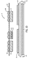
FIGS. 2-11 are schematic cross-sectional side views of a POL structure during various stages of a manufacturing/build-up process according to an embodiment of the invention. -
FIG. 12 is a schematic cross-sectional side view of a POL structure according to another embodiment of the invention. - Embodiments of the present invention provide for a surface-mount package having improved thermo-mechanical reliability, as well as a method of forming such a surface-mount package.
- Referring to
FIG. 1 , a surface-mount packaging andinterconnect structure 10 is shown according to an embodiment of the invention. In the embodiment shown inFIG. 1 , surface-mount package structure 10 is in the form of a power overlay (POL) structure, although it is recognized that other surface-mount package structures are considered to be within the scope of the invention. ThePOL structure 10 includes one or more semiconductor device(s) 12 therein that, according to various embodiments, may be in the form of a die, diode, or other power electronic device. As shown inFIG. 1 , three semiconductor device(s) 12 are provided inPOL structure 10, however, it is recognized that a greater or lesser number ofsemiconductor devices 12 could be included inPOL structure 10. The semiconductor device(s) 12 are packaged within aPOL sub-module 14 that forms a direct metallic connection to the power semiconductor device(s) 12, with the connection being in the form of a low profile, planar first-level interconnect structure, for example. - A second-level input-output (I/O)
connection 16 is provided onPOL sub-module 14 to enable surface mounting of thePOL structure 10 to an external circuit, such as a printed circuit board (PCB) (not shown). According to an exemplary embodiment, the second-level I/O connection 16 is formed of land grid array (LGA) solder bumps 17that are configured to be attached/affixed to the PCB to electrically couple thePOL structure 10 to the PCB, although other suitable second-level solder interconnections, such as ball grid array (BGA) solder bumps, could also be used. TheLGA solder bumps 17 provide a highly reliable interconnection structure that is resistive to failure in high stress conditions. - As shown in
FIG. 1 ,POL structure 10 also includes amulti-layer substrate structure 18 to whichPOL sub-module 14 is attached. According to an exemplary embodiment, thesubstrate structure 18 is composed of a ceramic tile (e.g., alumina) 20 with a layer of direct bond copper (DBC) 22, 24 bonded to both sides thereof by a high-temperature joining process, with thetop DBC layer 22 forming a "first surface" of thestructure 18 and thebottom DBC layer 24 forming a "second surface" of thestructure 18. For the joining process, different brazing and direct bond technologies may be employed based on, for example, whethertile 20 is composed of alumina or aluminum nitride and silicon nitride, etc. Thetop DBC layer 22, or "die side DBC layer," ofsubstrate structure 18 is then etched after firing, to pattern the layer as desired based on the number/arrangement ofsemiconductor devices 12. Thebottom DBC layer 24, or "non-die side DBC layer," on the backside of thesubstrate structure 18 is left fully or partially exposed to provide efficient heat transfer out from thePOL structure 10. While referred to above and here below as "DBC layers," it is recognized that aluminum can be used instead of copper as the metal layers, and thus such an embodiment is considered within the scope of the invention. Thus, use of the term "DBC layers" here below is meant to encompass asubstrate structure 18 that includes sheets of any suitablemetallic material 22, 24 (such as copper or aluminum) bonded to both sides of a ceramic tile (e.g., alumina) 20. As shown inFIG. 1 , a dielectric material 26 (i.e., "dielectric filler material") is also provided onPOL structure 10 to fill in gaps in thePOL structure 10, so as to provide additional structural integrity toPOL structure 10. According to the embodiment ofPOL structure 10 shown inFIG. 1 , thedielectric material 26 is in the form of a polymeric underfill (e.g., capillary underfill or no-flow underfill), encapsulate, silicone or molding compound. Alternatively, and as will be discussed below in greater detail with respect toFIG. 12 , it is recognized that thedielectric material 26 could be formed from a combination of a ceramic or dielectric sheet and an additional dielectric filler material (underfills, molding compounds, silicone or encapsulate). - The
POL structure 10 ofFIG. 1 is thus formed such that the second-level package I/O connections 16 are provided on the first-level interconnect side, for second-level interconnection to a PCB or other external circuit. The specific construction ofPOL structure 10 yields improved thermo-mechanical reliability and more robust second-level package I/O connections 16, along with superior electrical and thermal performance. - Referring now to
FIGS. 2-11 , detailed views of the process steps for a technique of manufacturing thePOL structure 10 ofFIG. 1 are provided, according to an embodiment of the invention. As shown first inFIGS. 2-9 , process steps for a build-up of thePOL sub-module 14 are provided. Referring toFIG. 2 , the build-up process ofPOL sub-module 14 begins with the placement and attachment of adielectric layer 30 or "flex layer" onto aframe structure 32. Thedielectric layer 30 is in the form of a lamination or film and is placed onframe structure 32 to provide stability during the build-up process ofPOL sub-module 14. According to embodiments of the invention, thedielectric layer 30 may be formed of one a plurality of dielectric materials, such as Kapton®, Ultem®, polytetrafluoroethylene (PTFE), Upilex®, polysulfone materials (e.g., Udel®, Radel®), or another polymer film, such as a liquid crystal polymer (LCP) or a polyimide material. - As shown in
FIG. 3 , upon securing ofdielectric layer 30 to framestructure 32, anadhesive layer 34 is deposited ontodielectric layer 30. A plurality ofvias 36 is then formed through theadhesive layer 34 anddielectric layer 30, as illustrated inFIG. 4 . According to embodiments of the invention, thevias 36 may be formed by way of a laser ablation or laser drilling process, plasma etching, photo-definition, or mechanical drilling processes. In a next step of technique, one or more semiconductor devices 12 (e.g., three semiconductor devices) are secured todielectric layer 30 by way ofadhesive layer 34, as illustrated inFIG. 5 . To secure thesemiconductor devices 12 todielectric layer 30, thesemiconductor devices 12 are placed ontoadhesive layer 34 and the adhesive 34 is then cured to secure thesemiconductor device 12 on thedielectric layer 30. According to one embodiment of the invention, and as shown inFIG. 5 ,semiconductor devices 12 may be of varying thickness/height. In order to increase a thickness/height of asemiconductor device 12, acopper shim 37 may be soldered to one or more ofsemiconductor devices 12 in order to increase its thickness/height so that the thickness/height of allsemiconductor devices 12 is equal and a back surface of thesemiconductor devices 12 is "planarized." - While the formation of
vias 36 throughadhesive layer 34 anddielectric lamination 30 is shown inFIG. 4 as being performed prior to placement ofsemiconductor devices 12 ontoadhesive layer 34, it is recognized that the placement ofsemiconductor devices 12 could occur prior to via formation. That is, depending on constraints imposed by via size,semiconductor devices 12 could first be placed onadhesive layer 34 anddielectric layer 30, with thevias 36 subsequently being formed at locations corresponding to a plurality of metalized circuits and/or connection pads (not shown) formed onsemiconductor devices 12. Furthermore, a combination of pre- and post-drilled vias could be employed as needed. - Referring now to
FIGS. 6 and 7 , upon securing ofsemiconductor devices 12 on thedielectric layer 30 and the formation ofvias 36, thevias 36 are cleaned (such as through a reactive ion etching (RIE) desoot process) and subsequently metalized to form first-level interconnects 38. The first-level metal interconnects 38 are typically formed through a combination of sputtering and electroplating applications, although it is recognized that other electroless methods of metal deposition could also be used. For example, a titanium adhesion layer and copper seed layer may first be applied via a sputtering process, followed by an electroplating process that increases a thickness of the copper to a desired level. The applied metal material is then subsequently patterned into metal interconnects 38 (i.e., first level interconnects) having a desired shape and that function as vertical feed-throughs formed throughdielectric layer 30 andadhesive layer 34. The metal interconnects 38 extend out from circuits and/or connection pads (not shown) ofsemiconductor devices 12, through vias/opening 36, and out across atop surface 39 ofdielectric layer 30. - As shown in
FIG. 8 , asolder mask layer 40 is applied over the patternedmetal interconnects 38 to provide a protective coating for the copper shims thereof. Alternative to solder, it is recognized that thelayer 40 could be composed of some metal material other than solder, such as Ni or Ni/Au. As further shown inFIG. 8 , the second-level I/O interconnections 16 are applied tosolder mask 40, on top of thedielectric layer 30. In one embodiment, I/O interconnections 16 are formed as LGA or BGA solder bumps 17 that are soldered tosolder mask 40 to enable surface mounting of thePOL structure 10 to an external circuit. The solder bumps 17 provide a highly reliable second-level interconnection structure that is resistive to failure in high stress conditions. - In completing the build-up of
POL sub-module 14, the POL sub-module 14 is singulated and removed fromframe structure 32, as illustrated inFIG. 9 . A completedPOL sub-module 14 is thus provided that includessemiconductor devices 12, first-level metal interconnects 38 that function as metal vertical feed-throughs, and second-level I/O interconnections 16 for surface-mounting of POL sub-module 14 to an external circuit, such as a PCB. ThePOL sub-module 14 is handled as a component or multi-chip module. - Referring now to
FIG. 10 , the technique of manufacturingPOL structure 10 continues with the formation of asubstrate structure 18 to be joined toPOL sub-module 14. Thesubstrate structure 18 is composed of a ceramic tile (e.g., alumina) 20 with die side and non-die side layers ofDBC FIG. 10 , the dieside DCB layer 22 ofsubstrate structure 18 is patterned, such as via an etching process, to correlate to the number/arrangement ofsemiconductor devices 12 ofPOL sub-module 14. According to an exemplary embodiment, the non-dieside DBC layer 24 on the backside of thesubstrate structure 18 is left unpatterned, as a continuous layer, so as to provide for greater bending strength of thesubstrate structure 18. Additionally, the entire surface of non-dieside DBC layer 24 is available for thermal connection (i.e., heatsink attachment). - As shown in
FIG. 11 , the technique of manufacturingPOL structure 10 continues with the attaching of POL sub-module 14 tosubstrate structure 18. According to one embodiment of the invention,POL sub-module 14 is attached tosubstrate structure 18 by way of asolder material 42, so as to secure the POL sub-module 14 andsubstrate structure 18 together. That is, each ofsemiconductor devices 12 is soldered to the dieside DBC layer 22. It is recognized, however, that a conductive adhesive or sintered silver could also be used instead of a solder material to secure the POL sub-module 14 andsubstrate structure 18 together. A polymeric underfill, encapsulate, or molding compound 26 (e.g., epoxy or other organic filler material) is then provided onPOL structure 10 that fills in gaps in thePOL structure 10, as shown inFIG. 11 , so as to constraindielectric layer 30 and provide additional electrical insulation and structural integrity to thePOL structure 10. - As shown in
FIGS. 10 and11 , according to an exemplary embodiment of the invention, formation of thesubstrate structure 18 is selectively performed so as to optimize thermal performance ofPOL structure 10. That is, it is recognized that there is a mismatch between the coefficient of thermal expansion (CTE) of the ceramic substrate 20 (which generally has a low CTE) and theunderfill 26 and copper pads/connections substrate structure 18, and that this CTE mismatch can lead to unbalanced thermal stresses inPOL structure 10 and thereby cause module warpage, bending stress, and cracking in the ceramic/insulatingsubstrate 20,underfill material 26, and/or the second-level I/O interconnections 16 (i.e., BGA/LGA solder bumps 17). The unbalanced thermal stresses inPOL structure 10, and the warpage, bending stress and cracking caused thereby, can be minimized by selective formation of thesubstrate structure 18. In formingsubstrate structure 18, a thickness (identified as 44) and area coverage (identified as 46) of non-dieside DBC layer 24 is selectively controlled so to optimize thermal performance ofPOL structure 10. More specifically, the ratio of a volume of non-dieside DBC layer 24 to the volume of the die-side DBC layer 22 is selected/controlled such that thermal/bending stresses in theunderfill 26 andceramic substrate 20 are reduced simultaneously to within acceptable levels. By providing additional DBC volume to layer 24 on the substrate back-side (i.e., non-die side), the thermal expansion of theDBC layer 24 on the non-die side can counteract the underfill/encapsulant 26 expansion on the die side of theceramic substrate 20, such that the thermal/bending stresses are reduced. - In determining an appropriate volume ratio/volume imbalance of the
non-die side DBC 24 to thedie side DBC 22, and acorresponding thickness 44 andarea coverage 46 ofDBC layer 24, the following factors are taken into consideration: (1) the volume of theunderfill material 26 and the known material properties thereof, including the elastic modulus, coefficient of thermal expansion (CTE), and fracture stress and toughness of the underfill material; (2) thedie 12 density, thickness and spacing within thePOL sub-module 14; and (3) the thickness and material properties of theceramic substrate 20, including the elastic modulus and CTE of the ceramic substrate. In general,stiffer underfill materials 26 require greater DBC volume imbalance between DBC layers 22, 24 to reduce module warpage and bending stress, whereas compliant underfill materials require lesser volume imbalance. - According to an exemplary embodiment of the invention, the DBC volume ratio/volume imbalance of the
non-die side DBC 24 and thedie side DBC 22 will be greater than 1 and less than 2.5, for a typicalorganic underfill material 26 for electronics packaging. That is, it is desired that the DBC volume ratio/volume imbalance be in this range because a balanced ceramic substrate (i.e., DBC Ratios ∼1) would exhibit high unbalanced thermal stress during thermal cycling and greater package curvature (warpage) due to high CTE-mismatch between the ceramic 20 (3-9 ppm/C) and typical organic underfills 26 (9-50ppm/C). By increasing the DBC volume ratio of thenon-die side DBC 24 to between 1 and 2.5 that of thedie side DBC 22, stress balance is provided that reduces POL package curvature and enables more robust second-level module interconnections 16. With respect to the above listed range of 1 to 2.5, it is recognized that the DBC volume ratio/volume imbalance of thenon-die side DBC 24 and thedie side DBC 22 could be less than 1 if the CTE ofunderfill material 26 is very low, such that the CTE mismatch is minimized. - Referring now to
FIG. 12 , aPOL structure 50 is shown according to another embodiment of the invention, where separate dielectric elements are used to fills in gaps in thePOL structure 50 betweendielectric layer 30 andsubstrate structure 18 in the area occupied by dies 12. As shown inFIG. 12 , a ceramic ordielectric sheet 52 is positioned betweendielectric layer 30 and themulti-layer substrate structure 18, adjacent thedielectric layer 30. The ceramic/dielectric sheet 52 includes cut-outs 54 formed therein to receive the dies 12 therein. A polymeric underfill material ormolding compound 56 is then positioned between the ceramic/dielectric sheet 52 and themulti-layer substrate structure 18, so as to fill-ingaps 58 between the ceramic/dielectric sheet 52 and the ceramic tile/alumina 20 of themulti-layer substrate structure 18. The implementing of ceramic/dielectric sheet 52 for filling-in a portion of the volume in thePOL structure 50 betweendielectric layer 30 andsubstrate structure 18, as opposed to entirely using only adielectric filler material 56, beneficially makes thePOL structure 50 less susceptible to moisture absorption and can further minimize thermo-mechanical stresses in thePOL structure 50 so as to reduce cracking, delaminations, etc. - With respect to
POL structure 50, it is recognized that the volume and the known thermo-mechanical material properties of each of the ceramic/dielectric sheet 52 and theunderfill material 56 are taken into account in determining an appropriate volume ratio/volume imbalance of thenon-die side DBC 24 to thedie side DBC 22, and acorresponding thickness 44 andarea coverage 46 ofDBC layer 24. The elastic modulus, coefficient of thermal expansion (CTE), and fracture stress and toughness of each of the ceramic/dielectric sheet 52 and theunderfill material 56 may differ from one another, and thus these material properties for each separate element are considered when determined the volume ratio/volume imbalance. - Beneficially, embodiments of the invention thus provide a POL packaging and
interconnect structure 10 having second-level package I/O's 16 that are provided on the flex side (i.e., on top of dielectric layer 30) of the POL sub-module 14 for second-level interconnection to an external circuit and the entire non-dieside DBC layer 24 is available for thermal connection. ThePOL structure 10 incorporates a stress balance-based design strategy that reduces package warpage and thermal stress, such that the package reliability in thermal cycling can be improved. Thermal expansion of the non-dieside DBC layer 24 counteracts the underfill/encapsulant expansion on the die side of theceramic substrate 20, with the resulting stress balance reducing package curvature and enabling more robust second-level module interconnections 16. A non-dieside DBC layer 24 can be formed to provide optimal DBC volume ratio/volume imbalance for a given package design (device size, density etc.), with the volume determination of the non-dieside DBC layer 24 being based on the package curvature requirement for second level assembly, along with the dielectric material and insulating material's bending strength and toughness. - Therefore, according to one embodiment of the invention, a surface-mount structure includes a sub-module having a dielectric layer and at least one semiconductor device attached to the dielectric layer, with each of the at least one semiconductor device including a substrate composed of a semiconductor material. The sub-module also includes a first level metal interconnect structure electrically coupled to the at least one semiconductor device that extends through vias formed through the dielectric layer so as to be connected to the at least one semiconductor device and a second level input/output (I/O) connection electrically coupled to the first level metal interconnect structure and formed on the dielectric layer on a side opposite the at least one semiconductor device, the second level I/O connection configured to connect the sub-module to an external circuit. The surface-mount structure also includes a multi-layer substrate structure having a first surface and a second surface, wherein the at least one semiconductor device of the sub-module is attached to the first surface of the multi-layer substrate. The surface-mount structure further includes one or more dielectric materials positioned between the dielectric layer and the first surface of the multi-layer substrate structure and at least partially about the at least one semiconductor device of the sub-module, the one or more dielectric materials configured to fill in gaps in the surface-mount structure and provide additional structural integrity thereto.
- According to another embodiment of the invention, a method of manufacturing a surface-mount packaging and interconnect structure includes the step of constructing a sub-module including at least one semiconductor device and a packaging structure formed thereabout, with the step of constructing the sub-module further including attaching the at least one semiconductor device to a dielectric layer, forming a first-level metallic interconnect structure over the dielectric that extends through vias in the dielectric layer to electrically connect to the at least one semiconductor device, and forming a second level input/output (I/O) connection on the dielectric layer on a side opposite the at least one semiconductor device, with the second level I/O connection configured to connect the sub-module to an external circuit. The method also includes the step of forming a substrate structure that includes a center substrate layer and first and second metallic layers on opposing sides of the center substrate layer, such that the first and second metallic layers form a first surface and a second surface, respectively, of the substrate structure. The method further includes the steps of attaching the sub-module to the first surface of the substrate structure and providing a dielectric filler material between the dielectric layer and the first surface of the substrate structure, the dielectric filler material at least partially encapsulating the at least one semiconductor device of the sub-module.
- According to yet another embodiment of the invention, a power overlay (POL) packaging structure includes a POL sub-module having a dielectric layer, a plurality of semiconductor devices attached to the dielectric layer, a first level interconnect structure electrically coupled to the plurality of semiconductor devices and extending through vias formed through the dielectric layer so as to be connected to the plurality of semiconductor devices, and a second level interconnect structure to electrically couple the POL sub-module to an external circuit structure, with the second level interconnect structure comprising a plurality of solder bumps formed over the dielectric layer and first level interconnect structure and configured to make an interconnection to the external circuit structure. The POL packaging structure also includes a multi-layer substrate structure having a first surface and a second surface, with the plurality of semiconductor devices of the POL sub-module being attached to the first surface of the multi-layer substrate structure. The multi-layer substrate structure of the POL packaging structure further includes a first direct bond copper (DBC) layer forming the first surface of the multi-layer substrate structure, a second DBC layer forming the second surface of the multi-layer substrate structure, and a ceramic layer sandwiched between the first and second DBC layers. The POL packaging structure further includes an encapsulate positioned between the dielectric layer and the first surface of the multi-layer substrate structure and at least partially about the plurality of semiconductor devices of the sub-module.
- While the invention has been described in detail in connection with only a limited number of embodiments, it should be readily understood that the invention is not limited to such disclosed embodiments. Rather, the invention can be modified to incorporate any number of variations, alterations, substitutions or equivalent arrangements not heretofore described, but which are commensurate with the spirit and scope of the invention. Additionally, while various embodiments of the invention have been described, it is to be understood that aspects of the invention may include only some of the described embodiments. Accordingly, the invention is not to be seen as limited by the foregoing description, but is only limited by the scope of the appended claims.
Claims (15)
- A surface-mount structure (10) comprising:a sub-module (14), the sub-module comprising:a dielectric layer (30);at least one semiconductor device (12) attached to the dielectric layer (30), with each of the at least one semiconductor device (12) including a substrate (18) composed of a semiconductor material;a first level metal interconnect structure (38) electrically coupled to the at least one semiconductor device (12), the metal interconnect structure (38) extending through vias (36) formed through the dielectric layer (30) so as to be connected to the at least one semiconductor device (12); anda second level input/output (I/O) connection (16) electrically coupled to the first level metal interconnect structure (38) and formed on the dielectric layer (30) on a side opposite the at least one semiconductor device (12), the second level I/O connection (16) configured to connect the sub-module (14) to an external circuit;a multi-layer substrate structure (18) having a first surface and a second surface, wherein the at least one semiconductor device (12) of the sub-module (14) is attached to the first surface of the multi-layer substrate (18); andone or more dielectric materials (26) positioned between the dielectric layer (30) and the first surface of the multi-layer substrate structure (18) and at least partially about the at least one semiconductor device (12) of the sub-module (14), the one or more dielectric materials (26) configured to fill in gaps (58) in the surface-mount structure (10) and provide additional structural integrity thereto.
- The surface-mount structure of claim 1, wherein the multi-layer substrate structure (18) comprises:a ceramic insulating layer (20);a first metallic layer (22) positioned on one side of the insulating layer (20) to form the first surface of the multi-layer substrate structure (18); anda second metallic layer (24) positioned on another side of the insulating layer (20) to form the second surface of the multi-layer substrate structure (18) .
- The surface-mount structure of claim 2, wherein the first and second metallic layers (22,24) comprise first and second direct bond copper (DBC) layers.
- The surface-mount structure of claim 3, wherein the first DBC layer (22) comprises a patterned DBC layer and the second DBC layer (24) comprises a patterned or unpatterned DBC layer.
- The surface-mount structure of claim 3 or 4, wherein a volume of the second DBC layer (24) is greater than a volume of the first DBC layer (22).
- The surface-mount structure of claim 5, wherein the volume of the second DBC layer (24) is between 1 and 2.5 times the volume of the first DBC layer (22).
- The surface-mount structure of claim 5 or 6, wherein a thickness or area of the second DBC layer (24), and the corresponding volume, is controlled based on at least one of a thickness and material properties of the one or more dielectric materials (26), a density, thickness, and spacing of the at least one semiconductor device (12), and a thickness and material properties of the ceramic insulating layer (20).
- The surface-mount structure of claim 7, wherein the material properties of the one or more dielectric materials (26) and the ceramic insulating layer (20) include at least one of an elastic modulus, coefficient of thermal expansion (CTE), and fracture stress and toughness.
- The surface-mount structure of any of claims 5 to 8, wherein a volume ratio between the second DBC layer (24) and the first DBC layer (22) provides a stress balanced surface-mount packaging and interconnect structure that minimizes warpage and thermal stresses therein.
- The surface-mount structure of any preceding claim, wherein the one or more dielectric materials (26) comprises an underfill material (56), encapsulant, silicone or molding compound positioned between the dielectric layer (30) and the first surface of the multi-layer substrate structure (18).
- The surface-mount structure of any preceding claim, wherein one or more dielectric materials (26) comprises:a ceramic or dielectric sheet (52) positioned between the dielectric layer (30) and the first surface of the multi-layer substrate structure (18), the ceramic or dielectric sheet (52) having cut-outs (54) formed therein to receive the at least one semiconductor device (12); anda dielectric filler material positioned between the ceramic or dielectric sheet (52) and the first surface of the multi-layer substrate structure (18) so as to fill-in gaps (58) between the ceramic or dielectric sheet (52) and the multi-layer substrate structure (18).
- The surface-mount structure of any preceding claim, wherein the second level I/O connection (16) comprises one of land grid array (LGA) solder bumps and ball grid array (BGA) solder bumps.
- The surface-mount structure of claim 12, further comprising one of a solder material (42), a conductive adhesive (34), or sintered metal joint positioned between the multi-layer substrate structure (18) and the sub-module (14) to secure the sub-module (14) to the multi-layer substrate structure (18).
- The surface-mount structure of any preceding claim, wherein the sub-module (14) comprises a power overlay (POL) sub-module.
- A method of manufacturing a surface-mount packaging and interconnect structure (10) comprising of:constructing a sub-module (14) including at least one semiconductor device (12) and a packaging structure formed thereabout, wherein constructing the sub-module (14) further includes:attaching the at least one semiconductor device (12) to a dielectric layer (30), forming a first-level metallic interconnect structure (38) over the dielectric layer (30) that extends through vias (36) in the dielectric layer (30) to electrically connect to the at least one semiconductor device (12); andforming a second level input/output (I/O) connection (16) on the dielectric layer (30) on a side opposite the at least one semiconductor device (12), with the second level I/O connection (16) configured to connect the sub-module (14) to an external circuit;forming a substrate structure (18) that includes a center substrate layer (20) and first and second metallic layers (22,24) on opposing sides of the center substrate layer (20), such that the first and second metallic layers (22,24) form a first surface and a second surface, respectively, of the substrate structure (18);attaching the sub-module (14) to the first surface of the substrate structure (18); andproviding a dielectric filler material (26) between the dielectric layer (30) and the first surface of the substrate structure (18), the dielectric filler material (26) at least partially encapsulating the at least one semiconductor device (12) of the sub-module (14).
Applications Claiming Priority (1)
| Application Number | Priority Date | Filing Date | Title |
|---|---|---|---|
| US13/561,811 US8941208B2 (en) | 2012-07-30 | 2012-07-30 | Reliable surface mount integrated power module |
Publications (3)
| Publication Number | Publication Date |
|---|---|
| EP2693472A2 true EP2693472A2 (en) | 2014-02-05 |
| EP2693472A3 EP2693472A3 (en) | 2017-08-09 |
| EP2693472B1 EP2693472B1 (en) | 2022-12-14 |
Family
ID=49035265
Family Applications (1)
| Application Number | Title | Priority Date | Filing Date |
|---|---|---|---|
| EP13177852.4A Active EP2693472B1 (en) | 2012-07-30 | 2013-07-24 | Power semiconductor module and its method of manufacturing |
Country Status (7)
| Country | Link |
|---|---|
| US (2) | US8941208B2 (en) |
| EP (1) | EP2693472B1 (en) |
| JP (1) | JP6302184B2 (en) |
| KR (1) | KR102088692B1 (en) |
| CN (3) | CN111508909B (en) |
| SG (1) | SG196753A1 (en) |
| TW (1) | TWI587477B (en) |
Families Citing this family (25)
| Publication number | Priority date | Publication date | Assignee | Title |
|---|---|---|---|---|
| US8804339B2 (en) * | 2011-02-28 | 2014-08-12 | Toyota Motor Engineering & Manufacturing North America, Inc. | Power electronics assemblies, insulated metal substrate assemblies, and vehicles incorporating the same |
| DE102011078811B3 (en) * | 2011-07-07 | 2012-05-24 | Semikron Elektronik Gmbh & Co. Kg | Power electronic system with a cooling device |
| KR20130129712A (en) * | 2012-05-21 | 2013-11-29 | 페어차일드코리아반도체 주식회사 | Semiconductor package and methods of fabricating the same |
| US8941208B2 (en) * | 2012-07-30 | 2015-01-27 | General Electric Company | Reliable surface mount integrated power module |
| US10269688B2 (en) | 2013-03-14 | 2019-04-23 | General Electric Company | Power overlay structure and method of making same |
| US8987876B2 (en) | 2013-03-14 | 2015-03-24 | General Electric Company | Power overlay structure and method of making same |
| US9312231B2 (en) * | 2013-10-31 | 2016-04-12 | Freescale Semiconductor, Inc. | Method and apparatus for high temperature semiconductor device packages and structures using a low temperature process |
| US9659837B2 (en) | 2015-01-30 | 2017-05-23 | Semiconductor Components Industries, Llc | Direct bonded copper semiconductor packages and related methods |
| JP6418126B2 (en) | 2015-10-09 | 2018-11-07 | 三菱電機株式会社 | Semiconductor device |
| US9443792B1 (en) * | 2015-10-31 | 2016-09-13 | Ixys Corporation | Bridging DMB structure for wire bonding in a power semiconductor device module |
| JP6403741B2 (en) * | 2016-09-30 | 2018-10-10 | 三菱電機株式会社 | Surface mount semiconductor package equipment |
| US9953917B1 (en) | 2016-12-12 | 2018-04-24 | General Electric Company | Electronics package with embedded through-connect and resistor structure and method of manufacturing thereof |
| US9953913B1 (en) | 2016-12-12 | 2018-04-24 | General Electric Company | Electronics package with embedded through-connect structure and method of manufacturing thereof |
| TWI648854B (en) * | 2017-06-14 | 2019-01-21 | Win Semiconductors Corp. | Improved structure for reducing deformation of compound semiconductor wafers |
| US10541153B2 (en) | 2017-08-03 | 2020-01-21 | General Electric Company | Electronics package with integrated interconnect structure and method of manufacturing thereof |
| US10541209B2 (en) | 2017-08-03 | 2020-01-21 | General Electric Company | Electronics package including integrated electromagnetic interference shield and method of manufacturing thereof |
| US10804115B2 (en) | 2017-08-03 | 2020-10-13 | General Electric Company | Electronics package with integrated interconnect structure and method of manufacturing thereof |
| US10332832B2 (en) | 2017-08-07 | 2019-06-25 | General Electric Company | Method of manufacturing an electronics package using device-last or device-almost last placement |
| US10892237B2 (en) * | 2018-12-14 | 2021-01-12 | General Electric Company | Methods of fabricating high voltage semiconductor devices having improved electric field suppression |
| DE102019121012B4 (en) * | 2019-08-02 | 2024-06-13 | Infineon Technologies Ag | Package and method for producing a package |
| US11398445B2 (en) | 2020-05-29 | 2022-07-26 | General Electric Company | Mechanical punched via formation in electronics package and electronics package formed thereby |
| CN118451543A (en) * | 2022-03-31 | 2024-08-06 | 华为技术有限公司 | Chip packaging structure, electronic equipment and preparation method of chip packaging structure |
| US12431402B2 (en) | 2022-07-26 | 2025-09-30 | Avago Technologies International Sales Pte. Limited | Stress and warpage improvements for stiffener ring package with exposed die(s) |
| TWI869906B (en) * | 2023-06-29 | 2025-01-11 | 同欣電子工業股份有限公司 | Pre-mold direct bond copper (dbc) substrate and manufacturing method thereof |
| GB2642027A (en) * | 2024-06-17 | 2025-12-31 | Cambridge Gan Devices Ltd | Fan-out panel-level packaging with a direct bonded copper substrate |
Family Cites Families (36)
| Publication number | Priority date | Publication date | Assignee | Title |
|---|---|---|---|---|
| US6104078A (en) * | 1994-03-09 | 2000-08-15 | Denso Corporation | Design for a semiconductor device having elements isolated by insulating regions |
| US5880530A (en) | 1996-03-29 | 1999-03-09 | Intel Corporation | Multiregion solder interconnection structure |
| US6404065B1 (en) | 1998-07-31 | 2002-06-11 | I-Xys Corporation | Electrically isolated power semiconductor package |
| US6306680B1 (en) | 1999-02-22 | 2001-10-23 | General Electric Company | Power overlay chip scale packages for discrete power devices |
| JP3683179B2 (en) | 2000-12-26 | 2005-08-17 | 松下電器産業株式会社 | Semiconductor device and manufacturing method thereof |
| JP4969738B2 (en) * | 2001-06-28 | 2012-07-04 | 株式会社東芝 | Ceramic circuit board and semiconductor module using the same |
| US6908784B1 (en) * | 2002-03-06 | 2005-06-21 | Micron Technology, Inc. | Method for fabricating encapsulated semiconductor components |
| DE10227658B4 (en) * | 2002-06-20 | 2012-03-08 | Curamik Electronics Gmbh | Metal-ceramic substrate for electrical circuits or modules, method for producing such a substrate and module with such a substrate |
| CN2613046Y (en) * | 2003-04-17 | 2004-04-21 | 威盛电子股份有限公司 | Chip packaging structure |
| JP3809168B2 (en) * | 2004-02-03 | 2006-08-16 | 株式会社東芝 | Semiconductor module |
| TWI245384B (en) * | 2004-12-10 | 2005-12-11 | Phoenix Prec Technology Corp | Package structure with embedded chip and method for fabricating the same |
| US7190581B1 (en) * | 2005-01-11 | 2007-03-13 | Midwest Research Institute | Low thermal resistance power module assembly |
| JP4207896B2 (en) * | 2005-01-19 | 2009-01-14 | 富士電機デバイステクノロジー株式会社 | Semiconductor device |
| JP4793622B2 (en) * | 2005-03-04 | 2011-10-12 | 日立金属株式会社 | Ceramic circuit board, power module, and method of manufacturing power module |
| US20070126085A1 (en) * | 2005-12-02 | 2007-06-07 | Nec Electronics Corporation | Semiconductor device and method of manufacturing the same |
| TWI279897B (en) * | 2005-12-23 | 2007-04-21 | Phoenix Prec Technology Corp | Embedded semiconductor chip structure and method for fabricating the same |
| US8018056B2 (en) | 2005-12-21 | 2011-09-13 | International Rectifier Corporation | Package for high power density devices |
| WO2007105361A1 (en) * | 2006-03-08 | 2007-09-20 | Kabushiki Kaisha Toshiba | Electronic component module |
| US8049338B2 (en) * | 2006-04-07 | 2011-11-01 | General Electric Company | Power semiconductor module and fabrication method |
| US7999369B2 (en) | 2006-08-29 | 2011-08-16 | Denso Corporation | Power electronic package having two substrates with multiple semiconductor chips and electronic components |
| KR101391924B1 (en) | 2007-01-05 | 2014-05-07 | 페어차일드코리아반도체 주식회사 | Semiconductor package |
| US20080190748A1 (en) * | 2007-02-13 | 2008-08-14 | Stephen Daley Arthur | Power overlay structure for mems devices and method for making power overlay structure for mems devices |
| DE102007041921A1 (en) * | 2007-09-04 | 2009-03-05 | Siemens Ag | Method for producing and contacting electronic components by means of a substrate plate, in particular DCB ceramic substrate plate |
| US8030752B2 (en) * | 2007-12-18 | 2011-10-04 | Samsung Electro-Mechanics Co., Ltd. | Method of manufacturing semiconductor package and semiconductor plastic package using the same |
| KR101610973B1 (en) * | 2008-03-17 | 2016-04-08 | 미쓰비시 마테리알 가부시키가이샤 | Substrate for power module with heat sink and method for producing the same, power module with heat sink, and substrate for power module |
| US8130507B2 (en) * | 2008-03-24 | 2012-03-06 | Ngk Spark Plug Co., Ltd. | Component built-in wiring board |
| US8358000B2 (en) * | 2009-03-13 | 2013-01-22 | General Electric Company | Double side cooled power module with power overlay |
| JP2010263080A (en) * | 2009-05-07 | 2010-11-18 | Denso Corp | Semiconductor device |
| US8409926B2 (en) * | 2010-03-09 | 2013-04-02 | Stats Chippac, Ltd. | Semiconductor device and method of forming insulating layer around semiconductor die |
| CN201667332U (en) * | 2010-03-29 | 2010-12-08 | 比亚迪股份有限公司 | A semiconductor power module |
| US8531027B2 (en) * | 2010-04-30 | 2013-09-10 | General Electric Company | Press-pack module with power overlay interconnection |
| JP2011253950A (en) * | 2010-06-02 | 2011-12-15 | Mitsubishi Electric Corp | Power semiconductor device |
| CN102339818B (en) | 2010-07-15 | 2014-04-30 | 台达电子工业股份有限公司 | Power module and manufacturing method thereof |
| US8114712B1 (en) * | 2010-12-22 | 2012-02-14 | General Electric Company | Method for fabricating a semiconductor device package |
| CN202135401U (en) * | 2011-05-30 | 2012-02-01 | 宝鸡市博瑞德金属材料有限公司 | High thermal conductivity aluminum substrate |
| US8941208B2 (en) * | 2012-07-30 | 2015-01-27 | General Electric Company | Reliable surface mount integrated power module |
-
2012
- 2012-07-30 US US13/561,811 patent/US8941208B2/en active Active
-
2013
- 2013-07-15 TW TW102125293A patent/TWI587477B/en active
- 2013-07-17 JP JP2013148095A patent/JP6302184B2/en active Active
- 2013-07-24 EP EP13177852.4A patent/EP2693472B1/en active Active
- 2013-07-25 SG SG2013056916A patent/SG196753A1/en unknown
- 2013-07-30 CN CN202010096033.6A patent/CN111508909B/en active Active
- 2013-07-30 CN CN201811531761.4A patent/CN110060962B/en active Active
- 2013-07-30 KR KR1020130090523A patent/KR102088692B1/en active Active
- 2013-07-30 CN CN201310324485.5A patent/CN103579137B/en active Active
-
2014
- 2014-11-19 US US14/547,667 patent/US9184124B2/en active Active
Non-Patent Citations (1)
| Title |
|---|
| None |
Also Published As
| Publication number | Publication date |
|---|---|
| TW201413916A (en) | 2014-04-01 |
| US9184124B2 (en) | 2015-11-10 |
| CN110060962A (en) | 2019-07-26 |
| US20140029234A1 (en) | 2014-01-30 |
| CN111508909A (en) | 2020-08-07 |
| CN110060962B (en) | 2023-09-26 |
| EP2693472A3 (en) | 2017-08-09 |
| SG196753A1 (en) | 2014-02-13 |
| JP6302184B2 (en) | 2018-03-28 |
| CN103579137A (en) | 2014-02-12 |
| KR20140016204A (en) | 2014-02-07 |
| US8941208B2 (en) | 2015-01-27 |
| JP2014027272A (en) | 2014-02-06 |
| TWI587477B (en) | 2017-06-11 |
| US20150069612A1 (en) | 2015-03-12 |
| EP2693472B1 (en) | 2022-12-14 |
| CN103579137B (en) | 2020-03-13 |
| KR102088692B1 (en) | 2020-03-13 |
| CN111508909B (en) | 2024-12-17 |
Similar Documents
| Publication | Publication Date | Title |
|---|---|---|
| US9184124B2 (en) | Reliable surface mount integrated power module | |
| US10186477B2 (en) | Power overlay structure and method of making same | |
| US8653635B2 (en) | Power overlay structure with leadframe connections | |
| CN104051377B (en) | Power cover structure and method of making the same | |
| EP1597947B1 (en) | Method for manufacturing an electronic module |
Legal Events
| Date | Code | Title | Description |
|---|---|---|---|
| AK | Designated contracting states |
Kind code of ref document: A2 Designated state(s): AL AT BE BG CH CY CZ DE DK EE ES FI FR GB GR HR HU IE IS IT LI LT LU LV MC MK MT NL NO PL PT RO RS SE SI SK SM TR |
|
| AX | Request for extension of the european patent |
Extension state: BA ME |
|
| PUAI | Public reference made under article 153(3) epc to a published international application that has entered the european phase |
Free format text: ORIGINAL CODE: 0009012 |
|
| RIC1 | Information provided on ipc code assigned before grant |
Ipc: H01L 23/538 20060101ALN20170328BHEP Ipc: H01L 23/31 20060101ALN20170328BHEP Ipc: H01L 21/56 20060101ALN20170328BHEP Ipc: H01L 23/373 20060101AFI20170328BHEP Ipc: H01L 23/48 20060101ALN20170328BHEP Ipc: H01L 25/07 20060101ALN20170328BHEP |
|
| PUAL | Search report despatched |
Free format text: ORIGINAL CODE: 0009013 |
|
| AK | Designated contracting states |
Kind code of ref document: A3 Designated state(s): AL AT BE BG CH CY CZ DE DK EE ES FI FR GB GR HR HU IE IS IT LI LT LU LV MC MK MT NL NO PL PT RO RS SE SI SK SM TR |
|
| AX | Request for extension of the european patent |
Extension state: BA ME |
|
| RIC1 | Information provided on ipc code assigned before grant |
Ipc: H01L 23/48 20060101ALN20170706BHEP Ipc: H01L 23/373 20060101AFI20170706BHEP Ipc: H01L 25/07 20060101ALN20170706BHEP Ipc: H01L 21/56 20060101ALN20170706BHEP Ipc: H01L 23/538 20060101ALN20170706BHEP Ipc: H01L 23/31 20060101ALN20170706BHEP |
|
| STAA | Information on the status of an ep patent application or granted ep patent |
Free format text: STATUS: REQUEST FOR EXAMINATION WAS MADE |
|
| 17P | Request for examination filed |
Effective date: 20180209 |
|
| RBV | Designated contracting states (corrected) |
Designated state(s): AL AT BE BG CH CY CZ DE DK EE ES FI FR GB GR HR HU IE IS IT LI LT LU LV MC MK MT NL NO PL PT RO RS SE SI SK SM TR |
|
| STAA | Information on the status of an ep patent application or granted ep patent |
Free format text: STATUS: EXAMINATION IS IN PROGRESS |
|
| 17Q | First examination report despatched |
Effective date: 20210420 |
|
| GRAP | Despatch of communication of intention to grant a patent |
Free format text: ORIGINAL CODE: EPIDOSNIGR1 |
|
| STAA | Information on the status of an ep patent application or granted ep patent |
Free format text: STATUS: GRANT OF PATENT IS INTENDED |
|
| INTG | Intention to grant announced |
Effective date: 20220725 |
|
| GRAS | Grant fee paid |
Free format text: ORIGINAL CODE: EPIDOSNIGR3 |
|
| GRAA | (expected) grant |
Free format text: ORIGINAL CODE: 0009210 |
|
| STAA | Information on the status of an ep patent application or granted ep patent |
Free format text: STATUS: THE PATENT HAS BEEN GRANTED |
|
| AK | Designated contracting states |
Kind code of ref document: B1 Designated state(s): AL AT BE BG CH CY CZ DE DK EE ES FI FR GB GR HR HU IE IS IT LI LT LU LV MC MK MT NL NO PL PT RO RS SE SI SK SM TR |
|
| REG | Reference to a national code |
Ref country code: GB Ref legal event code: FG4D |
|
| REG | Reference to a national code |
Ref country code: CH Ref legal event code: EP |
|
| REG | Reference to a national code |
Ref country code: DE Ref legal event code: R096 Ref document number: 602013083047 Country of ref document: DE |
|
| REG | Reference to a national code |
Ref country code: IE Ref legal event code: FG4D |
|
| REG | Reference to a national code |
Ref country code: AT Ref legal event code: REF Ref document number: 1538186 Country of ref document: AT Kind code of ref document: T Effective date: 20230115 |
|
| REG | Reference to a national code |
Ref country code: LT Ref legal event code: MG9D |
|
| REG | Reference to a national code |
Ref country code: NL Ref legal event code: MP Effective date: 20221214 |
|
| PG25 | Lapsed in a contracting state [announced via postgrant information from national office to epo] |
Ref country code: SE Free format text: LAPSE BECAUSE OF FAILURE TO SUBMIT A TRANSLATION OF THE DESCRIPTION OR TO PAY THE FEE WITHIN THE PRESCRIBED TIME-LIMIT Effective date: 20221214 Ref country code: NO Free format text: LAPSE BECAUSE OF FAILURE TO SUBMIT A TRANSLATION OF THE DESCRIPTION OR TO PAY THE FEE WITHIN THE PRESCRIBED TIME-LIMIT Effective date: 20230314 Ref country code: LT Free format text: LAPSE BECAUSE OF FAILURE TO SUBMIT A TRANSLATION OF THE DESCRIPTION OR TO PAY THE FEE WITHIN THE PRESCRIBED TIME-LIMIT Effective date: 20221214 Ref country code: FI Free format text: LAPSE BECAUSE OF FAILURE TO SUBMIT A TRANSLATION OF THE DESCRIPTION OR TO PAY THE FEE WITHIN THE PRESCRIBED TIME-LIMIT Effective date: 20221214 |
|
| REG | Reference to a national code |
Ref country code: AT Ref legal event code: MK05 Ref document number: 1538186 Country of ref document: AT Kind code of ref document: T Effective date: 20221214 |
|
| PG25 | Lapsed in a contracting state [announced via postgrant information from national office to epo] |
Ref country code: RS Free format text: LAPSE BECAUSE OF FAILURE TO SUBMIT A TRANSLATION OF THE DESCRIPTION OR TO PAY THE FEE WITHIN THE PRESCRIBED TIME-LIMIT Effective date: 20221214 Ref country code: LV Free format text: LAPSE BECAUSE OF FAILURE TO SUBMIT A TRANSLATION OF THE DESCRIPTION OR TO PAY THE FEE WITHIN THE PRESCRIBED TIME-LIMIT Effective date: 20221214 Ref country code: HR Free format text: LAPSE BECAUSE OF FAILURE TO SUBMIT A TRANSLATION OF THE DESCRIPTION OR TO PAY THE FEE WITHIN THE PRESCRIBED TIME-LIMIT Effective date: 20221214 Ref country code: GR Free format text: LAPSE BECAUSE OF FAILURE TO SUBMIT A TRANSLATION OF THE DESCRIPTION OR TO PAY THE FEE WITHIN THE PRESCRIBED TIME-LIMIT Effective date: 20230315 |
|
| PG25 | Lapsed in a contracting state [announced via postgrant information from national office to epo] |
Ref country code: NL Free format text: LAPSE BECAUSE OF FAILURE TO SUBMIT A TRANSLATION OF THE DESCRIPTION OR TO PAY THE FEE WITHIN THE PRESCRIBED TIME-LIMIT Effective date: 20221214 |
|
| PG25 | Lapsed in a contracting state [announced via postgrant information from national office to epo] |
Ref country code: SM Free format text: LAPSE BECAUSE OF FAILURE TO SUBMIT A TRANSLATION OF THE DESCRIPTION OR TO PAY THE FEE WITHIN THE PRESCRIBED TIME-LIMIT Effective date: 20221214 Ref country code: RO Free format text: LAPSE BECAUSE OF FAILURE TO SUBMIT A TRANSLATION OF THE DESCRIPTION OR TO PAY THE FEE WITHIN THE PRESCRIBED TIME-LIMIT Effective date: 20221214 Ref country code: PT Free format text: LAPSE BECAUSE OF FAILURE TO SUBMIT A TRANSLATION OF THE DESCRIPTION OR TO PAY THE FEE WITHIN THE PRESCRIBED TIME-LIMIT Effective date: 20230414 Ref country code: ES Free format text: LAPSE BECAUSE OF FAILURE TO SUBMIT A TRANSLATION OF THE DESCRIPTION OR TO PAY THE FEE WITHIN THE PRESCRIBED TIME-LIMIT Effective date: 20221214 Ref country code: EE Free format text: LAPSE BECAUSE OF FAILURE TO SUBMIT A TRANSLATION OF THE DESCRIPTION OR TO PAY THE FEE WITHIN THE PRESCRIBED TIME-LIMIT Effective date: 20221214 Ref country code: CZ Free format text: LAPSE BECAUSE OF FAILURE TO SUBMIT A TRANSLATION OF THE DESCRIPTION OR TO PAY THE FEE WITHIN THE PRESCRIBED TIME-LIMIT Effective date: 20221214 Ref country code: AT Free format text: LAPSE BECAUSE OF FAILURE TO SUBMIT A TRANSLATION OF THE DESCRIPTION OR TO PAY THE FEE WITHIN THE PRESCRIBED TIME-LIMIT Effective date: 20221214 |
|
| PG25 | Lapsed in a contracting state [announced via postgrant information from national office to epo] |
Ref country code: SK Free format text: LAPSE BECAUSE OF FAILURE TO SUBMIT A TRANSLATION OF THE DESCRIPTION OR TO PAY THE FEE WITHIN THE PRESCRIBED TIME-LIMIT Effective date: 20221214 Ref country code: PL Free format text: LAPSE BECAUSE OF FAILURE TO SUBMIT A TRANSLATION OF THE DESCRIPTION OR TO PAY THE FEE WITHIN THE PRESCRIBED TIME-LIMIT Effective date: 20221214 Ref country code: IS Free format text: LAPSE BECAUSE OF FAILURE TO SUBMIT A TRANSLATION OF THE DESCRIPTION OR TO PAY THE FEE WITHIN THE PRESCRIBED TIME-LIMIT Effective date: 20230414 Ref country code: AL Free format text: LAPSE BECAUSE OF FAILURE TO SUBMIT A TRANSLATION OF THE DESCRIPTION OR TO PAY THE FEE WITHIN THE PRESCRIBED TIME-LIMIT Effective date: 20221214 |
|
| REG | Reference to a national code |
Ref country code: DE Ref legal event code: R097 Ref document number: 602013083047 Country of ref document: DE |
|
| PLBE | No opposition filed within time limit |
Free format text: ORIGINAL CODE: 0009261 |
|
| STAA | Information on the status of an ep patent application or granted ep patent |
Free format text: STATUS: NO OPPOSITION FILED WITHIN TIME LIMIT |
|
| PG25 | Lapsed in a contracting state [announced via postgrant information from national office to epo] |
Ref country code: DK Free format text: LAPSE BECAUSE OF FAILURE TO SUBMIT A TRANSLATION OF THE DESCRIPTION OR TO PAY THE FEE WITHIN THE PRESCRIBED TIME-LIMIT Effective date: 20221214 |
|
| 26N | No opposition filed |
Effective date: 20230915 |
|
| PG25 | Lapsed in a contracting state [announced via postgrant information from national office to epo] |
Ref country code: SI Free format text: LAPSE BECAUSE OF FAILURE TO SUBMIT A TRANSLATION OF THE DESCRIPTION OR TO PAY THE FEE WITHIN THE PRESCRIBED TIME-LIMIT Effective date: 20221214 |
|
| PG25 | Lapsed in a contracting state [announced via postgrant information from national office to epo] |
Ref country code: MC Free format text: LAPSE BECAUSE OF FAILURE TO SUBMIT A TRANSLATION OF THE DESCRIPTION OR TO PAY THE FEE WITHIN THE PRESCRIBED TIME-LIMIT Effective date: 20221214 |
|
| PG25 | Lapsed in a contracting state [announced via postgrant information from national office to epo] |
Ref country code: MC Free format text: LAPSE BECAUSE OF FAILURE TO SUBMIT A TRANSLATION OF THE DESCRIPTION OR TO PAY THE FEE WITHIN THE PRESCRIBED TIME-LIMIT Effective date: 20221214 |
|
| REG | Reference to a national code |
Ref country code: CH Ref legal event code: PL |
|
| REG | Reference to a national code |
Ref country code: BE Ref legal event code: MM Effective date: 20230731 |
|
| PG25 | Lapsed in a contracting state [announced via postgrant information from national office to epo] |
Ref country code: LU Free format text: LAPSE BECAUSE OF NON-PAYMENT OF DUE FEES Effective date: 20230724 |
|
| PG25 | Lapsed in a contracting state [announced via postgrant information from national office to epo] |
Ref country code: LU Free format text: LAPSE BECAUSE OF NON-PAYMENT OF DUE FEES Effective date: 20230724 |
|
| REG | Reference to a national code |
Ref country code: IE Ref legal event code: MM4A |
|
| PG25 | Lapsed in a contracting state [announced via postgrant information from national office to epo] |
Ref country code: CH Free format text: LAPSE BECAUSE OF NON-PAYMENT OF DUE FEES Effective date: 20230731 |
|
| PG25 | Lapsed in a contracting state [announced via postgrant information from national office to epo] |
Ref country code: IT Free format text: LAPSE BECAUSE OF FAILURE TO SUBMIT A TRANSLATION OF THE DESCRIPTION OR TO PAY THE FEE WITHIN THE PRESCRIBED TIME-LIMIT Effective date: 20221214 Ref country code: BE Free format text: LAPSE BECAUSE OF NON-PAYMENT OF DUE FEES Effective date: 20230731 |
|
| PG25 | Lapsed in a contracting state [announced via postgrant information from national office to epo] |
Ref country code: IE Free format text: LAPSE BECAUSE OF NON-PAYMENT OF DUE FEES Effective date: 20230724 |
|
| PG25 | Lapsed in a contracting state [announced via postgrant information from national office to epo] |
Ref country code: IE Free format text: LAPSE BECAUSE OF NON-PAYMENT OF DUE FEES Effective date: 20230724 |
|
| PG25 | Lapsed in a contracting state [announced via postgrant information from national office to epo] |
Ref country code: BG Free format text: LAPSE BECAUSE OF FAILURE TO SUBMIT A TRANSLATION OF THE DESCRIPTION OR TO PAY THE FEE WITHIN THE PRESCRIBED TIME-LIMIT Effective date: 20221214 |
|
| PG25 | Lapsed in a contracting state [announced via postgrant information from national office to epo] |
Ref country code: BG Free format text: LAPSE BECAUSE OF FAILURE TO SUBMIT A TRANSLATION OF THE DESCRIPTION OR TO PAY THE FEE WITHIN THE PRESCRIBED TIME-LIMIT Effective date: 20221214 |
|
| PGFP | Annual fee paid to national office [announced via postgrant information from national office to epo] |
Ref country code: GB Payment date: 20250619 Year of fee payment: 13 |
|
| PGFP | Annual fee paid to national office [announced via postgrant information from national office to epo] |
Ref country code: FR Payment date: 20250620 Year of fee payment: 13 |
|
| PG25 | Lapsed in a contracting state [announced via postgrant information from national office to epo] |
Ref country code: CY Free format text: LAPSE BECAUSE OF FAILURE TO SUBMIT A TRANSLATION OF THE DESCRIPTION OR TO PAY THE FEE WITHIN THE PRESCRIBED TIME-LIMIT; INVALID AB INITIO Effective date: 20130724 |
|
| PG25 | Lapsed in a contracting state [announced via postgrant information from national office to epo] |
Ref country code: HU Free format text: LAPSE BECAUSE OF FAILURE TO SUBMIT A TRANSLATION OF THE DESCRIPTION OR TO PAY THE FEE WITHIN THE PRESCRIBED TIME-LIMIT; INVALID AB INITIO Effective date: 20130724 |
|
| PGFP | Annual fee paid to national office [announced via postgrant information from national office to epo] |
Ref country code: DE Payment date: 20250620 Year of fee payment: 13 |
|
| REG | Reference to a national code |
Ref country code: DE Ref legal event code: R079 Ref document number: 602013083047 Country of ref document: DE Free format text: PREVIOUS MAIN CLASS: H01L0023373000 Ipc: H10W0040250000 |
|
| PG25 | Lapsed in a contracting state [announced via postgrant information from national office to epo] |
Ref country code: TR Free format text: LAPSE BECAUSE OF FAILURE TO SUBMIT A TRANSLATION OF THE DESCRIPTION OR TO PAY THE FEE WITHIN THE PRESCRIBED TIME-LIMIT Effective date: 20221214 |