EP2693463A1 - Semiconductor device having amplification factor with less dependence on current value - Google Patents
Semiconductor device having amplification factor with less dependence on current value Download PDFInfo
- Publication number
- EP2693463A1 EP2693463A1 EP12763747.8A EP12763747A EP2693463A1 EP 2693463 A1 EP2693463 A1 EP 2693463A1 EP 12763747 A EP12763747 A EP 12763747A EP 2693463 A1 EP2693463 A1 EP 2693463A1
- Authority
- EP
- European Patent Office
- Prior art keywords
- semiconductor region
- electric current
- semiconductor
- semiconductor device
- contact
- Prior art date
- Legal status (The legal status is an assumption and is not a legal conclusion. Google has not performed a legal analysis and makes no representation as to the accuracy of the status listed.)
- Withdrawn
Links
Images




Classifications
-
- H—ELECTRICITY
- H10—SEMICONDUCTOR DEVICES; ELECTRIC SOLID-STATE DEVICES NOT OTHERWISE PROVIDED FOR
- H10D—INORGANIC ELECTRIC SEMICONDUCTOR DEVICES
- H10D10/00—Bipolar junction transistors [BJT]
- H10D10/01—Manufacture or treatment
-
- H—ELECTRICITY
- H10—SEMICONDUCTOR DEVICES; ELECTRIC SOLID-STATE DEVICES NOT OTHERWISE PROVIDED FOR
- H10D—INORGANIC ELECTRIC SEMICONDUCTOR DEVICES
- H10D10/00—Bipolar junction transistors [BJT]
- H10D10/01—Manufacture or treatment
- H10D10/051—Manufacture or treatment of vertical BJTs
-
- H—ELECTRICITY
- H10—SEMICONDUCTOR DEVICES; ELECTRIC SOLID-STATE DEVICES NOT OTHERWISE PROVIDED FOR
- H10D—INORGANIC ELECTRIC SEMICONDUCTOR DEVICES
- H10D10/00—Bipolar junction transistors [BJT]
- H10D10/40—Vertical BJTs
- H10D10/421—Vertical BJTs having both emitter-base and base-collector junctions ending at the same surface of the body
-
- H—ELECTRICITY
- H10—SEMICONDUCTOR DEVICES; ELECTRIC SOLID-STATE DEVICES NOT OTHERWISE PROVIDED FOR
- H10D—INORGANIC ELECTRIC SEMICONDUCTOR DEVICES
- H10D62/00—Semiconductor bodies, or regions thereof, of devices having potential barriers
- H10D62/10—Shapes, relative sizes or dispositions of the regions of the semiconductor bodies; Shapes of the semiconductor bodies
- H10D62/13—Semiconductor regions connected to electrodes carrying current to be rectified, amplified or switched, e.g. source or drain regions
- H10D62/137—Collector regions of BJTs
-
- H—ELECTRICITY
- H10—SEMICONDUCTOR DEVICES; ELECTRIC SOLID-STATE DEVICES NOT OTHERWISE PROVIDED FOR
- H10D—INORGANIC ELECTRIC SEMICONDUCTOR DEVICES
- H10D62/00—Semiconductor bodies, or regions thereof, of devices having potential barriers
- H10D62/10—Shapes, relative sizes or dispositions of the regions of the semiconductor bodies; Shapes of the semiconductor bodies
- H10D62/17—Semiconductor regions connected to electrodes not carrying current to be rectified, amplified or switched, e.g. channel regions
- H10D62/177—Base regions of bipolar transistors, e.g. BJTs or IGBTs
-
- H—ELECTRICITY
- H10—SEMICONDUCTOR DEVICES; ELECTRIC SOLID-STATE DEVICES NOT OTHERWISE PROVIDED FOR
- H10D—INORGANIC ELECTRIC SEMICONDUCTOR DEVICES
- H10D64/00—Electrodes of devices having potential barriers
- H10D64/20—Electrodes characterised by their shapes, relative sizes or dispositions
- H10D64/23—Electrodes carrying the current to be rectified, amplified, oscillated or switched, e.g. sources, drains, anodes or cathodes
- H10D64/231—Emitter or collector electrodes for bipolar transistors
-
- H—ELECTRICITY
- H10—SEMICONDUCTOR DEVICES; ELECTRIC SOLID-STATE DEVICES NOT OTHERWISE PROVIDED FOR
- H10D—INORGANIC ELECTRIC SEMICONDUCTOR DEVICES
- H10D62/00—Semiconductor bodies, or regions thereof, of devices having potential barriers
- H10D62/10—Shapes, relative sizes or dispositions of the regions of the semiconductor bodies; Shapes of the semiconductor bodies
- H10D62/124—Shapes, relative sizes or dispositions of the regions of semiconductor bodies or of junctions between the regions
- H10D62/126—Top-view geometrical layouts of the regions or the junctions
Definitions
- the present invention relates to a semiconductor device and specifically relates to a bipolar transistor of which the electric current gain has less dependence on the base electric current or on the collector electric current.
- a conventional bipolar transistor is known for the fact that the electric current gain is small in a very low electric-current level, large in a middle electric-current level and small again due to a high level injection effect in a high electric-current level.
- the electric current gain is 35 at the collector electric current of 100 pA, and increases by approximately one order of magnitude according to the increase of the collector electric current to reach the maximum gain of 400 at about 100 ⁇ A, and then decreases for larger collector electric current.
- FIG. 6 .12(A) in page 106 of non-patent document 2 this structure is a structure in which a high-concentration base region (graft base 127) is extended from an edge surface of an emitter 130 laterally to under the emitter and buried therein.
- graft base 127 graft base 127
- FIG. 1 illustrates a sectional view of a transistor having the graft base structure extracted from FIG. 6 .12(A) of non-patent document 2.
- FIG. 1 illustrates a sectional view of a transistor having the graft base structure extracted from FIG. 6 .12(A) of non-patent document 2.
- the high-concentration base region 127 is extended with a length of 0.35 ⁇ m from the edge of the emitter 130 to under the emitter and buried therein.
- the reference numeral 110 is the collector
- the reference numeral 121 is the intrinsic base
- the reference numeral 127 is the graft base
- the reference numeral 130 is the emitter.
- This graft base transistor is not developed for improving the electric current dependence of the electric current gain. Since the graft base transistor is developed for improving the high frequency characteristics, the operating range mainly covers large electric current and less emphasis is put on the very low electric-current level.
- the structure in which the high-concentration part of the high-concentration base region of the graft base transistor has contact with the emitter increases the leakage electric current between the emitter and the base. This may lead the decrease of the electric current gain in the very low electric-current level near the value of the leakage electric current. Therefore, the range of the collector electric current, for which the gain variation is small, is unfavorably narrowed. In addition, the breakdown voltage between the base and the emitter becomes small and the application voltage range of the transistor is narrowed, which is not preferable.
- a measure in which a high-impurity-concentration region is provided on the surface of the base so as to be separated from the emitter and enclose the emitter is taken to solve the above problems. Namely, this can be described in terms of a device structure as follows.
- this device is used as not only a transistor but also an amplifying sensor having a favorable linearity, this device is referred to as "semiconductor device”.
- the expression “have contact with ... on (a part of) a surface” includes a case in which a device is provided “on” the surface and a case in which a device is provided “in” the surface (refer to FIG. 3 as described later) .
- the term “opposite conductivity” means p-type (hole with regard to carrier) when the first conductivity is n-type (electron with regard to carrier) and n-type (electron with regard to carrier) when the first conductivity is p-type (hole with regard to carrier).
- the fourth semiconductor region of which the impurity concentration is larger than that of the second semiconductor region, is separated from the third semiconductor region, the increase of the leakage electric current and the decrease of the breakdown voltage due to the graft base transistor configuration are prevented.
- the separation distance therebetween is required to be a distance with which the breakdown voltage between the second semiconductor region and the third semiconductor region does not considerably decrease, such as 0.06 micron for 3 V breakdown voltage.
- the ratio (electric current gain) of the electric current flowing between the first semiconductor region and the third semiconductor region to the electric current required for the second semiconductor region (corresponding to the base electric current) becomes large.
- the increase of the electric current gain is prevented, when the fourth semiconductor region is provided.
- the distance between the third semiconductor region and the fourth semiconductor region is shorter than the diffusion length of the minority carriers in the second semiconductor region in order to achieve the effect of the prevention of the increase of this electric current gain.
- a semiconductor is silicon and the impurity concentration is about 1E18 atoms/cc, this distance is about 20 micron. Since the lifetimes of the minority carriers are controlled by the defect density (a cause of the recombination center, as described later), the impurity concentration and the temperature-time history at the time of manufacturing a device (including the cooling down time from a high temperature), the diffusion length which represented by the square root of "a product of the diffusion constant of the minority carriers and the lifetime thereof" depends on the impurity concentration and the processing condition of manufacturing a device.
- the fourth semiconductor region is not required to enclose the third semiconductor region by a closed shape.
- a semiconductor device according to the present invention can also be as follows.
- the semiconductor device according to (2) even when there is a part (the opening) which is not entirely enclosed by the fourth semiconductor region around the third semiconductor region, the increase of the electric current gain is prevented at the part in which the opposite conductivity carriers flow out of the fourth semiconductor region. Additionally, even when the part is shorter than the length of the opening, the effect of the present invention is achieved when the length of the opening is equal to or shorter than the length of the inner perimeter where the fourth semiconductor region encloses the third semiconductor region.
- the impurity concentration of the third semiconductor region is required to be larger than that of the second semiconductor region.
- FIG. 2 illustrates a plane view of a semiconductor device in an embodiment according to the present invention.
- FIG. 3 is a sectional view of the semiconductor device sectioned along the 1-2 dotted and dashed line in the plane view illustrated in FIG. 2 .
- the reference numeral 110 denotes the first semiconductor region.
- the reference numeral 111 denotes an insulating film which is provided on the first, second, third, fourth surfaces for the purpose of passivation.
- the reference numeral 120 denotes the second semiconductor region provided so as to be in contact with the surface of the first semiconductor region.
- the reference numeral 130 denotes the third semiconductor region provided so as to be in contact with the surface of the second semiconductor region.
- the reference numeral 140 denotes the fourth semiconductor region provided so as to be separated from the third semiconductor and be in contact with the surface of the second semiconductor region. Unlike graft base, the fourth semiconductor region is not buried under the third semiconductor region.
- the reference numeral 133 denotes a contact hole to the third semiconductor region provided in the insulating film 111
- the reference numeral 143 denotes a contact hole to the fourth semiconductor region provided in the insulating film 111. Electrodes for each region are omitted for simplicity.
- the surface impurity concentration of the second semiconductor region 120 is about 1E18 atoms/cc, and the second thickness (depth) is about 2 micron.
- the surface impurity concentration of the third semiconductor region is about 9E20 atoms/cc, and the third thickness is submicrometer which is equal to or smaller than 0.5 micron.
- the surface impurity concentration of the fourth semiconductor region 140 is 1E20 atoms/cc, and the fourth thickness is smaller than the third thickness.
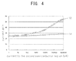
- the curve 14 depicted in FIG. 4 illustrates the dependence of the electric current gain on the electric current to the second semiconductor region of the fabricated semiconductor device.
- the electric current gain is already obtained as small as 1 pA.
- the electric current gain of this semiconductor device only increases from 24 to 28 for the 6-digit variation from 1 pA to 1000000 pA (1 ⁇ A) in the electric current to the second semiconductor region.
- the curve 12 depicted in FIG. 4 illustrates the electric current gain of a semiconductor device in which the fourth semiconductor region 140 is excluded in the structure illustrated in FIG. 2 , and the electric current gain of this device varies more than twice as much from 26 to 54 in reference for the variation from 1 pA to 1000000 pA in the electric current.
- the above comparison validates that the fourth semiconductor region according to one aspect of the present invention advantageously suppresses the variation of electric current gain.
- the electric current to the second semiconductor region is amplified at 1 pA even in a device in which the fourth semiconductor region is excluded.
- the surface impurity concentration of the second semiconductor region is smaller than that of the above fabrication conditions, for instance, approximately 1E17 atoms/cc or lower or when the clean MOS process is not employed, the second surface turns to depletion or inversion. Therefore, without the fourth semiconductor region, a leak channel may be formed on the second surface of the second semiconductor region to bypass between the third surface of the third semiconductor region and the first surface of the first semiconductor region, and the electric current gain may significantly decrease such as equal to or smaller than 1.
- the fourth semiconductor region since this leak channel is blocked the electric current gain is ensured even in a very low electric-current level.
- FIG. 5 illustrates an embodiment in which the shape of the fourth semiconductor region 140 is not a closed shape like an alphabet 0 but a planar shape having an opening like an alphabet C.
- the same reference numerals as in FIG. 2 mean the same regions and features.
- the reference numeral 44 denotes the dimension of the smallest part of the opening. In the semiconductor device illustrated in FIG. 5 , even an opening with a dimension of about 2-3 micron does not diminish an effect of suppressing the electric current dependence of the fourth current gain under the above described fabrication conditions in connection with FIG. 2 .
- FIG. 6 illustrates a plane view of an embodiment in which the present invention is applied to an amplifying photoelectric conversion device.
- the device is fabricated by use of the same design rule and fabrication techniques as in FIG. 2 .
- the reference numeral 120-0 denotes the second semiconductor region for photoelectric conversion, and forms a photodiode for converting light input P into photocurrent along with the first semiconductor region 110.
- the reference numeral 120-1 denotes the second semiconductor region (first base) of the first amplifying transistor which is in connection with this photodiode.
- the reference numeral 130-1 denotes the third semiconductor region (first emitter).
- the reference numeral 140-1 denotes the fourth semiconductor region.
- the reference numeral 120-2 denotes the second semiconductor region (second base) of the second amplifying transistor.
- the reference numeral 130-2 denotes the third semiconductor region (second emitter).
- the reference numeral 140-2 denotes the fourth semiconductor region.
- the third semiconductor region 130-1 of the first amplifying transistor is connected to the fourth semiconductor region 140-2 of the second amplifying transistor via thin film wiring 34 through a contact hole 133-1 and a contact hole 143-2. Since the second semiconductor region 120-2 (second base) of the second amplifying transistor is continuous with the fourth semiconductor region 140-2, the second semiconductor region 120-2 is connected to the third semiconductor region 130-1 (first emitter) of the first amplifying transistor.
- FIG. 6 illustrates that a lead out electrode 32 is provided through a contact hole 133-2 from the third semiconductor region 130-2.
- the gain is a product of each electric current gain of individual amplifying transistors.
- Amplified light electric current is obtained as Iout2 from the lead out electrode 32.
- pulse electric current for recharging electric charge which has been discharged by light electric current from the junction capacitors provided between the first semiconductor region 110 and the second semiconductor regions 120-0 and 120-1 is amplified and obtained from the lead out electrode 32.
- FIG. 7 illustrates direct-electric-current Iout2 (picoampere) obtained from the third semiconductor region 130-2 with reference to the light input energy P (picowatt) of the amplifying photoelectric conversion device illustrated in FIG. 6 .
- a voltage of 1.5 V is applied between the first semiconductor region and the third semiconductor region 130-2.
- the light source is He-Ne laser.
- Iout2 is proportional to P to the nth power
- a constant electric current gain is achieved with a simple configuration regardless of the electric current level. Therefore, by use of the semiconductor device according to one aspect of the present invention, an amplifying sensor with a small area is realized. As a result, a large-scale array is realized with high sensitivity amplifying sensor cells.
Landscapes
- Bipolar Transistors (AREA)
- Light Receiving Elements (AREA)
Abstract
Description
- The present invention relates to a semiconductor device and specifically relates to a bipolar transistor of which the electric current gain has less dependence on the base electric current or on the collector electric current.
- A conventional bipolar transistor is known for the fact that the electric current gain is small in a very low electric-current level, large in a middle electric-current level and small again due to a high level injection effect in a high electric-current level. For example, it is described as a typical example in pages 142-143 and
FIG. 7 ofnon-patent document 1 that the electric current gain is 35 at the collector electric current of 100 pA, and increases by approximately one order of magnitude according to the increase of the collector electric current to reach the maximum gain of 400 at about 100 µA, and then decreases for larger collector electric current. - On the other hand, a graft base transistor structure is conventionally known for achieving a small external base electric resistance and improving the high frequency characteristics. As illustrated in
FIG. 6 .12(A) in page 106 ofnon-patent document 2, this structure is a structure in which a high-concentration base region (graft base 127) is extended from an edge surface of anemitter 130 laterally to under the emitter and buried therein. In this case, when the high-concentration base region is separated from the emitter, the electric resistance from the region to anintrinsic base 121 under the center of the emitter becomes high and therefore this is not advantageous.FIG. 1 illustrates a sectional view of a transistor having the graft base structure extracted fromFIG. 6 .12(A) ofnon-patent document 2. InFIG. 1 , the high-concentration base region 127 is extended with a length of 0.35 µm from the edge of theemitter 130 to under the emitter and buried therein. InFIG. 1 , thereference numeral 110 is the collector, thereference numeral 121 is the intrinsic base, thereference numeral 127 is the graft base and thereference numeral 130 is the emitter. These reference numerals are overwritten inFIG. 6 .12(A). - This graft base transistor is not developed for improving the electric current dependence of the electric current gain. Since the graft base transistor is developed for improving the high frequency characteristics, the operating range mainly covers large electric current and less emphasis is put on the very low electric-current level.
- Thus, the structure in which the high-concentration part of the high-concentration base region of the graft base transistor has contact with the emitter increases the leakage electric current between the emitter and the base. This may lead the decrease of the electric current gain in the very low electric-current level near the value of the leakage electric current. Therefore, the range of the collector electric current, for which the gain variation is small, is unfavorably narrowed. In addition, the breakdown voltage between the base and the emitter becomes small and the application voltage range of the transistor is narrowed, which is not preferable.
-
- [NPL 1]
S.M.Sze, "Physics of Semiconductor Devices", second edition, John Wilyand Son. - [NPL 2]
L.Treitinger, M.Miura-Mattausch, "Ultra-Fast Silicon Bipolar Technology", Springer-Verlag - However, in order to amplify the current which varies by a factor of several orders of magnitude with a constant gain without using a complicated circuit, a bipolar transistor of which the electric current dependence of the electric current gain (the rate of output electric current (collector electric current or emitter electric current) to input electric current (base electric current) : β or hfe) is small in a several orders of magnitude is required.
- It is an object in the present invention to:
- 1) suppress the electric current gain variation occurred in the above conventional technique,
- 2) and, prevent the decrease of the breakdown voltage between the base and the emitter.
- In the present invention, a measure in which a high-impurity-concentration region is provided on the surface of the base so as to be separated from the emitter and enclose the emitter is taken to solve the above problems. Namely, this can be described in terms of a device structure as follows.
- (1)
A semiconductor device comprising:- a first semiconductor region having a first surface, a first thickness and a first conductivity;
- a second semiconductor region having a second surface, a second thickness, an opposite conductivity and in contact with the first semiconductor region at apart of the first surface;
- a third semiconductor region having a third surface, a third thickness, the first conductivity and in contact with the second semiconductor region at a part of the second surface; and
- a fourth semiconductor region having a fourth surface, a fourth thickness and in contact with the second semiconductor region at a part of the second surface,
- wherein, an impurity concentration of the third semiconductor region is larger than that of a part of the second semiconductor region which is in contact with the third semiconductor region, and the fourth semiconductor region is provided so as to be separated from the third semiconductor region and enclose the third semiconductor region and the impurity concentration of the fourth semiconductor region is larger than that of the second semiconductor region.
- Since this device is used as not only a transistor but also an amplifying sensor having a favorable linearity, this device is referred to as "semiconductor device".
- In addition, the expression "have contact with ... on (a part of) a surface" includes a case in which a device is provided "on" the surface and a case in which a device is provided "in" the surface (refer to
FIG. 3 as described later) . Also, the term "opposite conductivity" means p-type (hole with regard to carrier) when the first conductivity is n-type (electron with regard to carrier) and n-type (electron with regard to carrier) when the first conductivity is p-type (hole with regard to carrier). - In the present invention, since the fourth semiconductor region, of which the impurity concentration is larger than that of the second semiconductor region, is separated from the third semiconductor region, the increase of the leakage electric current and the decrease of the breakdown voltage due to the graft base transistor configuration are prevented. The separation distance therebetween is required to be a distance with which the breakdown voltage between the second semiconductor region and the third semiconductor region does not considerably decrease, such as 0.06 micron for 3 V breakdown voltage.
- It is known that the reason why "the electric current gain is small in the very low electric-current level" in the conventional transistor is the bulk recombination of minority carriers at the bulk recombination center in the second semiconductor region and the surface recombination caused at the surface recombination center on the second surface of the second semiconductor region.
- Since the effects of these recombinations become small when the electric current flowing between the first semiconductor region and the third semiconductor region (corresponding to the collector electric current and the emitter electric current) becomes large, the ratio (electric current gain) of the electric current flowing between the first semiconductor region and the third semiconductor region to the electric current required for the second semiconductor region (corresponding to the base electric current) becomes large. However, in an electric current level in which the effect of the surface recombination is small, the increase of the electric current gain is prevented, when the fourth semiconductor region is provided.
- It is desirable that the distance between the third semiconductor region and the fourth semiconductor region is shorter than the diffusion length of the minority carriers in the second semiconductor region in order to achieve the effect of the prevention of the increase of this electric current gain. When a semiconductor is silicon and the impurity concentration is about 1E18 atoms/cc, this distance is about 20 micron. Since the lifetimes of the minority carriers are controlled by the defect density (a cause of the recombination center, as described later), the impurity concentration and the temperature-time history at the time of manufacturing a device (including the cooling down time from a high temperature), the diffusion length which represented by the square root of "a product of the diffusion constant of the minority carriers and the lifetime thereof" depends on the impurity concentration and the processing condition of manufacturing a device.
- The fourth semiconductor region is not required to enclose the third semiconductor region by a closed shape. A semiconductor device according to the present invention can also be as follows.
- (2)
A semiconductor device according to (1) described above, wherein the fourth semiconductor region includes an opening in a plane shape which encloses the third semiconductor region, and a dimension of a shortest distance of the opening is equal to or smaller than one-tenth of a length of an inner perimeter of the plane shape which encloses the third semiconductor region. - In the semiconductor device according to (2), even when there is a part (the opening) which is not entirely enclosed by the fourth semiconductor region around the third semiconductor region, the increase of the electric current gain is prevented at the part in which the opposite conductivity carriers flow out of the fourth semiconductor region. Additionally, even when the part is shorter than the length of the opening, the effect of the present invention is achieved when the length of the opening is equal to or shorter than the length of the inner perimeter where the fourth semiconductor region encloses the third semiconductor region.
-
- (3)
In order to achieve the prevention of the increase of this electric current gain, the impurity concentration of the fourth semiconductor region is more than or equal to 10 times as large as that of the second semiconductor region. - In order to increase the electric current gain to be equal to or larger than 1, the impurity concentration of the third semiconductor region is required to be larger than that of the second semiconductor region.
- Although, conventionally, feedback loops are added to an analog amplifier circuit employing a number of transistors in order to achieve a constant electric current gain which is independent of the electric current level, in a semiconductor device in the present invention an almost constant electric current gain regardless of the electric current level is achieved by employing a simple structure.
-
- [
FIG. 1 ]
FIG. 1 is a sectional view of a conventional graft base transistor. - [
FIG. 2 ]
FIG. 2 is a plane view illustrating an embodiment according to the present invention. - [
FIG. 3 ]
FIG. 3 is a sectional view in the embodiment illustrated inFIG. 2 . - [
FIG. 4 ]
FIG. 4 illustrates the electric current dependence of the gain regarding a semiconductor device manufactured with reference to the plane view in the embodiment illustrated inFIG. 2 . - [
FIG. 5 ]
FIG. 5 is a plane view exemplifying an opening in the plane shape of the fourth semiconductor region. - [
FIG. 6 ]
FIG. 6 illustrates an embodiment in which one aspect of the present invention is applied to an amplifying photoelectric conversion device. - [
FIG. 7 ]
FIG. 7 illustrates electrical properties in the embodiment illustrated inFIG. 6 . -
FIG. 2 illustrates a plane view of a semiconductor device in an embodiment according to the present invention.FIG. 3 is a sectional view of the semiconductor device sectioned along the 1-2 dotted and dashed line in the plane view illustrated inFIG. 2 . In the diagrams, thereference numeral 110 denotes the first semiconductor region. The reference numeral 111 denotes an insulating film which is provided on the first, second, third, fourth surfaces for the purpose of passivation. Thereference numeral 120 denotes the second semiconductor region provided so as to be in contact with the surface of the first semiconductor region. Thereference numeral 130 denotes the third semiconductor region provided so as to be in contact with the surface of the second semiconductor region. Thereference numeral 140 denotes the fourth semiconductor region provided so as to be separated from the third semiconductor and be in contact with the surface of the second semiconductor region. Unlike graft base, the fourth semiconductor region is not buried under the third semiconductor region. Thereference numeral 133 denotes a contact hole to the third semiconductor region provided in the insulating film 111, and thereference numeral 143 denotes a contact hole to the fourth semiconductor region provided in the insulating film 111. Electrodes for each region are omitted for simplicity. - An n-type (100) face oriented silicon substrate with a resistivity of 10-20 Ωcm is used as the
first semiconductor region 110. The surface impurity concentration of thesecond semiconductor region 120 is about 1E18 atoms/cc, and the second thickness (depth) is about 2 micron. The surface impurity concentration of the third semiconductor region is about 9E20 atoms/cc, and the third thickness is submicrometer which is equal to or smaller than 0.5 micron. The surface impurity concentration of thefourth semiconductor region 140 is 1E20 atoms/cc, and the fourth thickness is smaller than the third thickness. With these configurations, a semiconductor device according to one aspect of the present invention as illustrated inFIGS. 2 and3 is manufactured by use of a CMOS process. - The
curve 14 depicted inFIG. 4 illustrates the dependence of the electric current gain on the electric current to the second semiconductor region of the fabricated semiconductor device. In this semiconductor device, the electric current gain is already obtained as small as 1 pA. The electric current gain of this semiconductor device only increases from 24 to 28 for the 6-digit variation from 1 pA to 1000000 pA (1 µA) in the electric current to the second semiconductor region. By contrast, thecurve 12 depicted inFIG. 4 illustrates the electric current gain of a semiconductor device in which thefourth semiconductor region 140 is excluded in the structure illustrated inFIG. 2 , and the electric current gain of this device varies more than twice as much from 26 to 54 in reference for the variation from 1 pA to 1000000 pA in the electric current. The above comparison validates that the fourth semiconductor region according to one aspect of the present invention advantageously suppresses the variation of electric current gain. - Since a clean MOS process is employed in this fabrication example, the electric current to the second semiconductor region is amplified at 1 pA even in a device in which the fourth semiconductor region is excluded. However, when the surface impurity concentration of the second semiconductor region is smaller than that of the above fabrication conditions, for instance, approximately 1E17 atoms/cc or lower or when the clean MOS process is not employed, the second surface turns to depletion or inversion. Therefore, without the fourth semiconductor region, a leak channel may be formed on the second surface of the second semiconductor region to bypass between the third surface of the third semiconductor region and the first surface of the first semiconductor region, and the electric current gain may significantly decrease such as equal to or smaller than 1. Here, with the fourth semiconductor region provided, since this leak channel is blocked the electric current gain is ensured even in a very low electric-current level.
-
FIG. 5 illustrates an embodiment in which the shape of thefourth semiconductor region 140 is not a closed shape like analphabet 0 but a planar shape having an opening like an alphabet C. InFIG. 5 , the same reference numerals as inFIG. 2 mean the same regions and features. Thereference numeral 44 denotes the dimension of the smallest part of the opening. In the semiconductor device illustrated inFIG. 5 , even an opening with a dimension of about 2-3 micron does not diminish an effect of suppressing the electric current dependence of the fourth current gain under the above described fabrication conditions in connection withFIG. 2 . -
FIG. 6 illustrates a plane view of an embodiment in which the present invention is applied to an amplifying photoelectric conversion device. The device is fabricated by use of the same design rule and fabrication techniques as inFIG. 2 . The reference numeral 120-0 denotes the second semiconductor region for photoelectric conversion, and forms a photodiode for converting light input P into photocurrent along with thefirst semiconductor region 110. The reference numeral 120-1 denotes the second semiconductor region (first base) of the first amplifying transistor which is in connection with this photodiode. The reference numeral 130-1 denotes the third semiconductor region (first emitter). The reference numeral 140-1 denotes the fourth semiconductor region. The reference numeral 120-2 denotes the second semiconductor region (second base) of the second amplifying transistor. The reference numeral 130-2 denotes the third semiconductor region (second emitter). The reference numeral 140-2 denotes the fourth semiconductor region. - The third semiconductor region 130-1 of the first amplifying transistor is connected to the fourth semiconductor region 140-2 of the second amplifying transistor via
thin film wiring 34 through a contact hole 133-1 and a contact hole 143-2. Since the second semiconductor region 120-2 (second base) of the second amplifying transistor is continuous with the fourth semiconductor region 140-2, the second semiconductor region 120-2 is connected to the third semiconductor region 130-1 (first emitter) of the first amplifying transistor. - Consequently, the light electric current converted by the
first semiconductor region 110 and the second semiconductor region 120-0 is amplified by the first and second amplifying transistors and obtained from the third semiconductor region 130-2 or the first semiconductor region.FIG. 6 illustrates that a lead outelectrode 32 is provided through a contact hole 133-2 from the third semiconductor region 130-2. The gain is a product of each electric current gain of individual amplifying transistors. - Amplified light electric current is obtained as Iout2 from the lead out
electrode 32. In addition, when pulse driving is performed between thefirst semiconductor region 110 and the third semiconductor region 130-2, pulse electric current for recharging electric charge which has been discharged by light electric current from the junction capacitors provided between thefirst semiconductor region 110 and the second semiconductor regions 120-0 and 120-1 is amplified and obtained from the lead outelectrode 32. -
FIG. 7 illustrates direct-electric-current Iout2 (picoampere) obtained from the third semiconductor region 130-2 with reference to the light input energy P (picowatt) of the amplifying photoelectric conversion device illustrated inFIG. 6 . A voltage of 1.5 V is applied between the first semiconductor region and the third semiconductor region 130-2. The light source is He-Ne laser. As illustrated inFIG. 7 , almost linear output electric current Iout2 is obtained with reference to the light input energy P. When it is assumed that Iout2 is proportional to P to the nth power, n = 1.07 is obtained as a result, which is approximate to n = 1. - With a semiconductor device according to one aspect of the present invention, a constant electric current gain is achieved with a simple configuration regardless of the electric current level. Therefore, by use of the semiconductor device according to one aspect of the present invention, an amplifying sensor with a small area is realized. As a result, a large-scale array is realized with high sensitivity amplifying sensor cells.
-
- 12: Curve illustrating the electric current dependence of the electric current gain of the semiconductor device in which the fourth semiconductor region is excluded 14: Curve illustrating the electric current dependence of the electric current gain of the semiconductor device in which the fourth semiconductor region is provided according to one aspect of the present invention
- 32: Electrode
- 34: Thin film wiring
- 44: Dimension of the smallest opening of the fourth semiconductor region
- 110: First semiconductor region
- 111: First insulating film
- 120: Second semiconductor region
- 120-0: Second semiconductor region for photoelectric conversion
- 120-1: Second semiconductor region of the first amplifying
- transistor
- 120-2: Second semiconductor region of the second amplifying transistor
- 130: Third semiconductor region
- 130-1: Third semiconductor region of the first amplifying transistor
- 130-2: Third semiconductor region of the second amplifying transistor
- 133 Contact hole to the third semiconductor region
- 133-1: Contact hole to the third semiconductor region of the first amplifying transistor
- 133-2: Contact hole to the third semiconductor region of the second amplifying transistor
- 140: Fourth semiconductor region
- 143: Contact hole to the fourth semiconductor region
- 143-2: Contact hole to the fourth semiconductor region of the second amplifying transistor
Claims (3)
- A semiconductor device comprising:a first semiconductor region having a first surface, a first thickness and a first conductivity;a second semiconductor region having a second surface, a second thickness, an opposite conductivity and in contact with the first semiconductor region at apart of the first surface;a third semiconductor region having a third surface, a third thickness, the first conductivity and in contact with the second semiconductor region at a part of the second surface; anda fourth semiconductor region having a fourth surface, a fourth thickness and in contact with the second semiconductor region at a part of the second surface,wherein, an impurity concentration of the third semiconductor region is larger than that of a part of the second semiconductor region which is in contact with the third semiconductor region, and the fourth semiconductor region is provided so as to be separated from the third semiconductor region and enclose the third semiconductor region and the impurity concentration of the fourth semiconductor region is larger than that of the second semiconductor region.
- The semiconductor device according to claim 1, wherein the fourth semiconductor region includes an opening in a plane shape which encloses the third semiconductor region, and a dimension of a smallest distance of the opening is smaller than or equal to one-tenth of a length of an inner perimeter of the plane shape which encloses the third semiconductor region.
- The semiconductor device according to claim 1, wherein a surface impurity concentration of the fourth semiconductor region is more than or equal to ten times as much as that of the second semiconductor region.
Applications Claiming Priority (2)
| Application Number | Priority Date | Filing Date | Title |
|---|---|---|---|
| JP2011069468A JP5750723B2 (en) | 2011-03-28 | 2011-03-28 | Method for suppressing change in amplification factor of semiconductor device against current change, photoelectric conversion element, and method for manufacturing semiconductor device |
| PCT/JP2012/052256 WO2012132539A1 (en) | 2011-03-28 | 2012-02-01 | Semiconductor device having amplification factor with less dependence on current value |
Publications (2)
| Publication Number | Publication Date |
|---|---|
| EP2693463A1 true EP2693463A1 (en) | 2014-02-05 |
| EP2693463A4 EP2693463A4 (en) | 2014-09-17 |
Family
ID=46930306
Family Applications (1)
| Application Number | Title | Priority Date | Filing Date |
|---|---|---|---|
| EP12763747.8A Withdrawn EP2693463A4 (en) | 2011-03-28 | 2012-02-01 | SEMICONDUCTOR DEVICE HAVING AMPLIFYING FACTOR WITH DEPENDENCE ON CURRENT VALUE |
Country Status (5)
| Country | Link |
|---|---|
| US (1) | US8921213B2 (en) |
| EP (1) | EP2693463A4 (en) |
| JP (1) | JP5750723B2 (en) |
| CN (1) | CN103460355B (en) |
| WO (1) | WO2012132539A1 (en) |
Families Citing this family (1)
| Publication number | Priority date | Publication date | Assignee | Title |
|---|---|---|---|---|
| EP3931854A1 (en) * | 2019-02-26 | 2022-01-05 | ASML Netherlands B.V. | Charged particle detector with gain element |
Family Cites Families (12)
| Publication number | Priority date | Publication date | Assignee | Title |
|---|---|---|---|---|
| US4881111A (en) * | 1977-02-24 | 1989-11-14 | Harris Corporation | Radiation hard, high emitter-base breakdown bipolar transistor |
| JPS61114574A (en) * | 1984-11-09 | 1986-06-02 | Hitachi Ltd | semiconductor equipment |
| JPH0626217B2 (en) * | 1987-11-11 | 1994-04-06 | 日本電気株式会社 | Method for manufacturing semiconductor device |
| JPH0319346A (en) * | 1989-06-16 | 1991-01-28 | Toyota Autom Loom Works Ltd | Semiconductor device |
| JP3037710B2 (en) * | 1990-02-28 | 2000-05-08 | キヤノン株式会社 | Semiconductor device and electronic device using the semiconductor device |
| JPH05166825A (en) * | 1991-12-17 | 1993-07-02 | Hitachi Ltd | Semiconductor device |
| JP2852241B2 (en) * | 1996-05-30 | 1999-01-27 | 山形日本電気株式会社 | Semiconductor device and manufacturing method thereof |
| JPH11176836A (en) * | 1997-12-05 | 1999-07-02 | Sony Corp | Semiconductor device and manufacturing method thereof |
| US6555894B2 (en) * | 1998-04-20 | 2003-04-29 | Intersil Americas Inc. | Device with patterned wells and method for forming same |
| JP2000235983A (en) * | 1999-02-16 | 2000-08-29 | Nec Corp | Semiconductor device and manufacturing method thereof |
| JP4707203B2 (en) * | 1999-09-09 | 2011-06-22 | ローム株式会社 | Semiconductor device |
| JP2001189318A (en) * | 1999-12-28 | 2001-07-10 | Nec Corp | Bipolar transistor and method of manufacturing the same |
-
2011
- 2011-03-28 JP JP2011069468A patent/JP5750723B2/en not_active Expired - Fee Related
-
2012
- 2012-02-01 EP EP12763747.8A patent/EP2693463A4/en not_active Withdrawn
- 2012-02-01 WO PCT/JP2012/052256 patent/WO2012132539A1/en not_active Ceased
- 2012-02-01 CN CN201280016617.1A patent/CN103460355B/en not_active Expired - Fee Related
-
2013
- 2013-09-27 US US14/039,719 patent/US8921213B2/en not_active Expired - Fee Related
Also Published As
| Publication number | Publication date |
|---|---|
| WO2012132539A1 (en) | 2012-10-04 |
| US8921213B2 (en) | 2014-12-30 |
| JP5750723B2 (en) | 2015-07-22 |
| CN103460355A (en) | 2013-12-18 |
| EP2693463A4 (en) | 2014-09-17 |
| JP2012204724A (en) | 2012-10-22 |
| US20140030878A1 (en) | 2014-01-30 |
| CN103460355B (en) | 2016-03-02 |
Similar Documents
| Publication | Publication Date | Title |
|---|---|---|
| CN1998091B (en) | Silicon photomultiplier and silicon photomultiplier unit | |
| US6455858B1 (en) | Semiconductor radiation detector | |
| JP5211095B2 (en) | Photodetector | |
| US7768090B2 (en) | Semiconductor photodetector device | |
| US9768340B2 (en) | Photodiode with a dark current suppression junction | |
| US20090261441A1 (en) | Optical semiconductor device | |
| US20140159180A1 (en) | Semiconductor resistor structure and semiconductor photomultiplier device | |
| US3745424A (en) | Semiconductor photoelectric transducer | |
| EP2175497B1 (en) | Avalanche photodiode for ultraviolet photon detection | |
| JPS62109376A (en) | Light receiving semiconductor device | |
| RU2494497C2 (en) | Mos-diode cell of solid radiation detector | |
| JPS5895877A (en) | Semiconductor photoelectric conversion device | |
| US8921213B2 (en) | Method of making less electric current dependence of electric current gain of semiconductor device | |
| Sinha et al. | Effect of heavy doping on the properties of high-low junction | |
| US20120326260A1 (en) | Photodiode that incorporates a charge balanced set of alternating n and p doped semiconductor regions | |
| JP5604901B2 (en) | Current amplification element | |
| CN110914995A (en) | Semiconductor device with single electron counting capability comprising avalanche bipolar transistor | |
| JP5218370B2 (en) | Current amplification circuit and light detection device | |
| EP0116652B1 (en) | Phototransistor | |
| EP3996137B1 (en) | Semiconductor device | |
| KR102891611B1 (en) | light detecting device | |
| RU2559161C1 (en) | Metal semiconductor device | |
| JPH0637349A (en) | Avalance photodiode doped with platinum | |
| Baliga | An improved GAMBIT device structure | |
| RU2583955C1 (en) | Capacitive mos diode cell of photodetector-radiation detector |
Legal Events
| Date | Code | Title | Description |
|---|---|---|---|
| PUAI | Public reference made under article 153(3) epc to a published international application that has entered the european phase |
Free format text: ORIGINAL CODE: 0009012 |
|
| 17P | Request for examination filed |
Effective date: 20131001 |
|
| AK | Designated contracting states |
Kind code of ref document: A1 Designated state(s): AL AT BE BG CH CY CZ DE DK EE ES FI FR GB GR HR HU IE IS IT LI LT LU LV MC MK MT NL NO PL PT RO RS SE SI SK SM TR |
|
| DAX | Request for extension of the european patent (deleted) | ||
| A4 | Supplementary search report drawn up and despatched |
Effective date: 20140814 |
|
| RIC1 | Information provided on ipc code assigned before grant |
Ipc: H01L 29/10 20060101ALI20140808BHEP Ipc: H01L 29/732 20060101ALI20140808BHEP Ipc: H01L 21/331 20060101AFI20140808BHEP |
|
| STAA | Information on the status of an ep patent application or granted ep patent |
Free format text: STATUS: THE APPLICATION HAS BEEN WITHDRAWN |
|
| 18W | Application withdrawn |
Effective date: 20170116 |