EP2692016B1 - Drahtlose kommunikationsvorrichtung mit passiven nebeneinander angeordnenten rahmenantennen und zugehörige verfahren - Google Patents
Drahtlose kommunikationsvorrichtung mit passiven nebeneinander angeordnenten rahmenantennen und zugehörige verfahren Download PDFInfo
- Publication number
- EP2692016B1 EP2692016B1 EP12711292.8A EP12711292A EP2692016B1 EP 2692016 B1 EP2692016 B1 EP 2692016B1 EP 12711292 A EP12711292 A EP 12711292A EP 2692016 B1 EP2692016 B1 EP 2692016B1
- Authority
- EP
- European Patent Office
- Prior art keywords
- antenna
- passive
- passive loop
- antennas
- loop
- Prior art date
- Legal status (The legal status is an assumption and is not a legal conclusion. Google has not performed a legal analysis and makes no representation as to the accuracy of the status listed.)
- Active
Links
- 238000004891 communication Methods 0.000 title claims description 38
- 238000000034 method Methods 0.000 title claims description 12
- 239000004020 conductor Substances 0.000 claims description 49
- 239000000758 substrate Substances 0.000 claims description 22
- 238000004519 manufacturing process Methods 0.000 claims description 6
- 239000003990 capacitor Substances 0.000 description 42
- 230000005855 radiation Effects 0.000 description 27
- 230000001965 increasing effect Effects 0.000 description 24
- 230000004044 response Effects 0.000 description 21
- 230000010287 polarization Effects 0.000 description 9
- 230000008878 coupling Effects 0.000 description 8
- 238000010168 coupling process Methods 0.000 description 8
- 238000005859 coupling reaction Methods 0.000 description 8
- RYGMFSIKBFXOCR-UHFFFAOYSA-N Copper Chemical compound [Cu] RYGMFSIKBFXOCR-UHFFFAOYSA-N 0.000 description 6
- 239000002184 metal Substances 0.000 description 6
- 229910052751 metal Inorganic materials 0.000 description 6
- 229910052802 copper Inorganic materials 0.000 description 5
- 239000010949 copper Substances 0.000 description 5
- 238000010586 diagram Methods 0.000 description 5
- 230000000694 effects Effects 0.000 description 5
- 230000008901 benefit Effects 0.000 description 4
- 239000000919 ceramic Substances 0.000 description 4
- 238000009413 insulation Methods 0.000 description 4
- 239000000463 material Substances 0.000 description 4
- 238000004804 winding Methods 0.000 description 4
- 238000013459 approach Methods 0.000 description 3
- 230000007423 decrease Effects 0.000 description 3
- 238000013461 design Methods 0.000 description 3
- 238000005259 measurement Methods 0.000 description 3
- 238000012360 testing method Methods 0.000 description 3
- 239000004593 Epoxy Substances 0.000 description 2
- 230000001413 cellular effect Effects 0.000 description 2
- 230000008859 change Effects 0.000 description 2
- 230000003247 decreasing effect Effects 0.000 description 2
- 238000009826 distribution Methods 0.000 description 2
- 239000011521 glass Substances 0.000 description 2
- 230000001939 inductive effect Effects 0.000 description 2
- 238000002955 isolation Methods 0.000 description 2
- 238000006842 Henry reaction Methods 0.000 description 1
- 241000220317 Rosa Species 0.000 description 1
- 239000011324 bead Substances 0.000 description 1
- 230000009286 beneficial effect Effects 0.000 description 1
- 230000005540 biological transmission Effects 0.000 description 1
- 230000010267 cellular communication Effects 0.000 description 1
- 150000001875 compounds Chemical class 0.000 description 1
- 238000010276 construction Methods 0.000 description 1
- MPTQRFCYZCXJFQ-UHFFFAOYSA-L copper(II) chloride dihydrate Chemical compound O.O.[Cl-].[Cl-].[Cu+2] MPTQRFCYZCXJFQ-UHFFFAOYSA-L 0.000 description 1
- PTVDYARBVCBHSL-UHFFFAOYSA-N copper;hydrate Chemical compound O.[Cu] PTVDYARBVCBHSL-UHFFFAOYSA-N 0.000 description 1
- 230000003467 diminishing effect Effects 0.000 description 1
- 238000002474 experimental method Methods 0.000 description 1
- 238000010438 heat treatment Methods 0.000 description 1
- 239000012212 insulator Substances 0.000 description 1
- 230000010354 integration Effects 0.000 description 1
- 239000011159 matrix material Substances 0.000 description 1
- 238000010295 mobile communication Methods 0.000 description 1
- 238000005457 optimization Methods 0.000 description 1
- 238000005549 size reduction Methods 0.000 description 1
- 238000004513 sizing Methods 0.000 description 1
- 239000007787 solid Substances 0.000 description 1
- 230000007704 transition Effects 0.000 description 1
- 229910000859 α-Fe Inorganic materials 0.000 description 1
Images


Classifications
-
- H—ELECTRICITY
- H01—ELECTRIC ELEMENTS
- H01Q—ANTENNAS, i.e. RADIO AERIALS
- H01Q1/00—Details of, or arrangements associated with, antennas
- H01Q1/12—Supports; Mounting means
- H01Q1/22—Supports; Mounting means by structural association with other equipment or articles
- H01Q1/24—Supports; Mounting means by structural association with other equipment or articles with receiving set
-
- H—ELECTRICITY
- H01—ELECTRIC ELEMENTS
- H01Q—ANTENNAS, i.e. RADIO AERIALS
- H01Q7/00—Loop antennas with a substantially uniform current distribution around the loop and having a directional radiation pattern in a plane perpendicular to the plane of the loop
-
- H—ELECTRICITY
- H01—ELECTRIC ELEMENTS
- H01Q—ANTENNAS, i.e. RADIO AERIALS
- H01Q1/00—Details of, or arrangements associated with, antennas
- H01Q1/12—Supports; Mounting means
- H01Q1/22—Supports; Mounting means by structural association with other equipment or articles
- H01Q1/24—Supports; Mounting means by structural association with other equipment or articles with receiving set
- H01Q1/241—Supports; Mounting means by structural association with other equipment or articles with receiving set used in mobile communications, e.g. GSM
- H01Q1/242—Supports; Mounting means by structural association with other equipment or articles with receiving set used in mobile communications, e.g. GSM specially adapted for hand-held use
- H01Q1/243—Supports; Mounting means by structural association with other equipment or articles with receiving set used in mobile communications, e.g. GSM specially adapted for hand-held use with built-in antennas
-
- H—ELECTRICITY
- H01—ELECTRIC ELEMENTS
- H01Q—ANTENNAS, i.e. RADIO AERIALS
- H01Q21/00—Antenna arrays or systems
- H01Q21/06—Arrays of individually energised antenna units similarly polarised and spaced apart
-
- H—ELECTRICITY
- H01—ELECTRIC ELEMENTS
- H01Q—ANTENNAS, i.e. RADIO AERIALS
- H01Q21/00—Antenna arrays or systems
- H01Q21/06—Arrays of individually energised antenna units similarly polarised and spaced apart
- H01Q21/061—Two dimensional planar arrays
-
- H—ELECTRICITY
- H01—ELECTRIC ELEMENTS
- H01Q—ANTENNAS, i.e. RADIO AERIALS
- H01Q5/00—Arrangements for simultaneous operation of antennas on two or more different wavebands, e.g. dual-band or multi-band arrangements
- H01Q5/30—Arrangements for providing operation on different wavebands
- H01Q5/378—Combination of fed elements with parasitic elements
- H01Q5/385—Two or more parasitic elements
-
- Y—GENERAL TAGGING OF NEW TECHNOLOGICAL DEVELOPMENTS; GENERAL TAGGING OF CROSS-SECTIONAL TECHNOLOGIES SPANNING OVER SEVERAL SECTIONS OF THE IPC; TECHNICAL SUBJECTS COVERED BY FORMER USPC CROSS-REFERENCE ART COLLECTIONS [XRACs] AND DIGESTS
- Y10—TECHNICAL SUBJECTS COVERED BY FORMER USPC
- Y10T—TECHNICAL SUBJECTS COVERED BY FORMER US CLASSIFICATION
- Y10T29/00—Metal working
- Y10T29/49—Method of mechanical manufacture
- Y10T29/49002—Electrical device making
- Y10T29/49016—Antenna or wave energy "plumbing" making
Definitions
- the present invention relates to the field of communications, and, more particularly, to antennas and related methods.
- Antennas may be used for a variety of purposes, such as communications or navigation, and portable radio devices may include broadcast receivers, pagers, or radio location devices ("ID tags").
- the cellular telephone is an example of a wireless communications device, which is nearly ubiquitous. A relatively small size, increased efficiency, and a relatively broad radiation pattern are generally desired characteristics of an antenna for a portable radio or wireless device. Additionally, as the functionality of a wireless device continues to increase, so too does the demand for a smaller wireless device which is easier and more convenient for users to carry.
- One challenge this poses for wireless device manufacturers is designing antennas that provide desired operating characteristics within the relatively limited amount of space available for antennas. For example, it may be desirable for an antenna to communicate over multiple frequency bands and at lower frequencies.
- antenna size may be based upon operating frequency or frequencies. For example, an antenna may become increasingly larger as the operating frequency decreases. Reducing the wavelength may reduce the size of the antenna, but a longer wavelengths may be desired for enhanced propagation.
- HF high frequencies
- 3 to 30 MHz for example, used for long-range communications
- efficient antennas for example, transmitting antennas
- wire antennas may be required at fixed stations.
- it may become increasingly important in these wireless communication applications to reduce not only the antenna size, but also to design and manufacture a reduced size antenna having the greatest gain for the smallest area over the desired frequency bands.
- the instantaneous 3 dB gain bandwidth, also known as half power fixed tuned radiation bandwidth, of electrically small antennas is thought to be limited under the Chu-Harrington limit (" Physical Limitations Of Omni-Directional Antennas, L.J. Chu, Journal of Applied Physics, Vol. 19, pp 1163 -1175, Dec. 1948 ).
- Canonical antennas include dipole and the loop antennas, in line and circle shapes. They translate and rotate electric currents to realize the divergence and curl functions, for example.
- Various coils may form hybrids of the dipole and the loop.
- Antennas may be linear, planar, or volumetric in form, e.g., they may be nearly 1, 2 or 3 dimensional.
- Optimal envelopes for antenna sizing may be Euclidian geometries such as a line, a circle, and a sphere, which may provide increased optimization of a relatively short distance between two points, increased area for circumference, and increased volume for decreased surface area respectively. It may be desirable to know the antennas that provide the greatest radiation bandwidth in these sizes.
- a broadband electrically large (r > ⁇ /2 ⁇ ) antenna for example, the spiral antenna, may provide a high pass response with theoretically unlimited bandwidth above a lower cutoff.
- the spiral may provide only a quadratic, bandpass type response with greatly limited bandwidth.
- Planar antennas may be increasingly valuable for their ease of manufacture and product integration.
- the elementary planar dipole may be formed by radial electric currents flowing on a metal disc (" Theory Of The Circular Diffraction Antenna," A. A. Pistolkors, Proceedings of the Institute Of Radio Engineers, Jan 1948, pp 56-60 ). Circular and linear notches for feeding may be desired.
- a circle of wire may give the same radiation pattern, and it may be preferred for ease of driving. Elements to extend the bandwidth of wire loop antennas may be desired. Radio wave expansion occurs at the speed of light. If the speed of light were reduced, antenna size would also be reduced.
- U.S. Patent Application Publication No. 2009/0212774 to Bosshard et al discloses an antenna arrangement for a magnetic resonance apparatus.
- the antenna arrangement includes at least four individually operable antenna conductor loops arranged in a matrix (i.e., rows and columns) configuration. Two antenna conductor loops adjacent in a row or column are inductively decoupled from one another, while two antenna loops diagonally adjacent to one another are capacitively decoupled from one another.
- U.S. Patent Application Publication No. 2009/0009414 to Reykowsi discloses an antenna array.
- the antenna array includes multiple Individual antennas arranged next to one another.
- the individual antennas are arranged within a radio- frequency closed conductor loop with capacitors inserted in each conductor loop.
- U.S. Patent Application Publication No. 2010/0121180 to Biber et al discloses a head coil to a magnetic resonance device.
- a number of antenna elements are carried by a supporting body.
- the supporting body has an end section that is shaped as a spherical cap.
- a butterfly antenna is mounted at the end of the section, and is annularly surrounded by at least one group antenna that overlaps the butterfly antenna.
- none of these approaches are focused on providing an antenna with multi-band frequency operation, while being small in size, and having desired gain for area.
- JP 2006-340246 A discloses a directivity control antenna system.
- US 2005/0088342 A1 discloses an annular ring antenna.
- US 2007/0139285 A1 discloses a loop antenna unit and a radio communication medium processor.
- US 2009/0009414 A1 discloses an antenna array.
- US 6,236,368 discloses a loop directive antenna.
- US 2004/0100410 A1 discloses a built-in multiband mobile phone antenna assembly.
- a wireless communications device that includes a housing and wireless communications circuitry carried by the housing.
- the wireless communications device also includes an antenna assembly carried by the housing and coupled to the wireless communications circuitry, for example.
- the antenna assembly includes a substrate, and a plurality of passive loop antennas carried by the substrate and arranged in side -by-side relation.
- Each of the plurality of passive loop antennas includes a passive loop conductor and a tuning element coupled thereto, for example.
- the antenna assembly also includes an active loop antenna carried by the substrate and arranged to be at least partially coextensive with each of the plurality of passive loop antennas.
- the active loop antenna includes an active loop conductor and a pair of feedpoints defined therein, for example. Accordingly, the antenna assembly has a relatively reduced size, while maintaining performance, for example, by providing multi-band frequency operation, and providing increased gain with respect to area.
- Each of the plurality of passive loop antennas has a respective straight side adjacent each neighboring passive antenna.
- Each of the plurality of passive loop antennas may have a polygonal shape, for example.
- the polygonal shape may be one of a square shape, a hexagonal shape, and a triangular shape.
- Each of the plurality of passive loop antennas may have a same size and shape.
- the active loop antenna may have a circular shape, for example.
- the plurality of passive loop antennas may define a center point.
- the active loop antenna may be concentric with the center point, for example.
- Each of the tuning elements may include a capacitor, for example.
- the plurality of passive loop antennas may be positioned on a first side of the substrate and the active loop antenna is positioned on a second side of the substrate, for example.
- Each of the passive loop conductors and the active loop conductor comprises an insulated wire.
- a method aspect is directed to a method of making an antenna assembly to be carried by a housing and to be coupled to wireless communications circuitry.
- the method includes positioning a plurality of passive loop antennas to be carried by a substrate in side-by-side relation.
- Each of the plurality of passive loop antennas includes a passive loop conductor and a tuning element coupled thereto, for example.
- the method also includes positioning an active loop antenna to be carried by the substrate and to be at least partially coextensive with each of the plurality of passive loop antennas.
- the active loop antenna includes an active loop conductor and a pair of feedpoints defined therein, for example.
- a wireless communications device 10 includes a housing 11 and wireless communications circuitry 12 carried by the housing.
- the wireless communications circuitry 12 may be cellular communications circuitry or radiolocation tag circuitry, for example, and be configured to communicate voice and/or data.
- the wireless circuitry 12 may be configured to communicate over a plurality of frequency bands, for example, cellular, WiFi, and global positioning system (GPS) bands.
- GPS global positioning system
- the wireless communications circuitry 12 may be configured to communicate over other frequency bands.
- Other circuitry for example, a controller 13 may be carried by the housing 11 and coupled to wireless communications circuitry 12.
- the wireless communications device 10 may include an input device (not shown), for example, input keys and/or a microphone, and an output device (not shown), for example, a display and/or speaker, coupled to the controller 13 and/or wireless communications circuitry 12.
- the wireless communications device 10 also includes an antenna assembly 20 carried by the housing 11 and coupled to the wireless communications circuitry 12.
- the antenna assembly 20 illustratively includes a substrate 21.
- the substrate 21 may be a printed circuit board substrate, for example, and may carry other components, as will be appreciated by those skilled in the art.
- the antenna assembly 20 also includes three same-sized hexagonal shaped passive loop antennas 22a-22c carried by the substrate 21.
- the passive loop antennas 22a-22c are arranged in a side -by-side relation. In the illustrated embodiment, each of the three passive loop antennas 22a-22c has a respective straight side adjacent each neighboring passive antenna.
- the passive loop antennas 22a-22c each have a circumference of 0.5 wavelengths or less at the operating frequency, e.g., the passive radiating loop antennas are naturally resonant or electrically small relative to the wavelength.
- each of the hexagonal passive loop antennas 22a-22c may be considered as an individual antenna element such that the combined electrical characteristics act like a loop antenna array.
- the hexagonal shape of the passive loop antennas 22a-22c creates a honeycomb lattice which advantageously provides an increased efficiency usage of space.
- the hexagonal tiling of space filling polyedra may be particularly advantageous in a portable wireless communications device where the housing 21 is relatively limited in size.
- the hexagonal shape of the passive loop antennas develop an increased radiation resistance at a reduced conductor loss for an increased efficiency gain and reduced overall size.
- Each of the passive loop antennas 22a-22c includes a passive loop conductor 27a-27c and a tuning element 28 coupled thereto.
- the tuning element 28 determines the frequency band of a particular passive loop antenna 22, and not the size thereof. Instead, the size of each passive loop antenna 22 is related to the gain of the antenna assembly 20 at the frequency band corresponding to the respective passive loop antenna.
- Each passive loop antenna 22 also includes a dielectric insulation layer 29 surrounding the passive loop conductor 27.
- each passive loop antenna 22 may be an insulated wire.
- the tuning element 28 is illustratively a capacitor and coupled inline with the passive loop conductor 27.
- the tuning element 28 may be another type of component, for example, an inductor, and may not be coupled inline, for example, a ferrite bead may instead surround the passive loop conductor 27 and the dielectric insulation layer 29.
- the tuning element 28 is a capacitor, for example, the passive loop antennas 22a-22c become electrically loaded so that they operate at a smaller physical size and/or lower frequency. Thus, the tuning element 28, or capacitor, reduces the size.
- the active loop antenna 23 cooperates with the passive loop antennas 22a-22c by inductive coupling such that the passive loop antennas act as three independent tunable antennas.
- Independent tuning of each of the passive loop antennas 22a-22c is accomplished by selecting or changing the value of each of the tuning elements 28, in particular, the capacitance.
- the antenna assembly 20 also includes an active loop antenna 23 carried by the substrate 21.
- the active loop antenna 23 illustratively has a circular shape and is partially coextensive with each of the plurality of passive loop antennas 22a-22c. In other words, the areas of the active loop antenna 23 and passive loop antennas 22a-22c may overlap without touching one another.
- the active loop antenna includes an active loop conductor 25 and a pair of feedpoints 26a, 26b defined therein.
- the active loop antenna 23 may also include an insulation layer 36 surrounding the active loop conductor 25. In other words, the active loop antenna 23 may also be an insulated wire.
- the respective insulation layers advantageously provide dielectric spacing between the passive loop antennas 22a-22c and the active loop antenna 23 so that they do not short circuit.
- the side-by-side relation of the passive loop antennas 22a-22c defines a center point 24, and the active loop antenna 23 is illustratively concentric with the center point.
- the active loop antenna 23 may not be concentric with the center point 24 in other embodiments.
- adjustment of an amount of offset may affect an amount of power coupled to each of the passive loop antennas 22a-22c.
- a feed conductor 31 or cable may couple the antenna assembly 20 to the wireless communications circuitry 12 via the feedpoints 26a, 26b.
- the feed conductor 31 may be coaxial cable, for example, and may include a center conductor 32 coupled to one of the feedpoints 26a, 26b and an outer conductor 34 coupled to the other of the feedbpoints, and separated from the inner conductor by a dielectric layer 33.
- Other types of cables or conductors may be used, such as, for example, a twisted pair of insulated wire.
- the feed cable 31 may itself become an antenna.
- the active loop antenna 23 may provide a balun to reduce the effect of the feed cable 31 inadvertently becoming an antenna.
- the passive loop antennas 22a-22c do not have a direct current (DC) connection to the feed cable 31 (i.e., there is no conductive contact, but rather inductive coupling).
- the active loop antenna 23 may also function as balun or "isolation transformer" to reduce common mode currents on coaxial feedlines, for example.
- a graph 50 is shown of the measured frequency response, or voltage standing wave ratio, of a multiple band prototype antenna assembly similar to the antenna assembly 20 as illustrated in FIG. 1 .
- the prototype antenna assembly included three hexagonal passive loop antennas and a circular active loop antenna.
- a first capacitor had a value of 30 picofarads
- a second capacitor was 10 picofarads
- a third capacitor was 20 picofarads.
- each passive loop antenna loop had a different value tuning capacitor.
- the graph 50 illustratively includes three bands, 51a, 51b, 51c at about 86 MHz, 106 MHz, and 144 MHz respectively, that were independently realized based upon the values of the respective capacitors.
- a summary of the multiple band prototype is as follows: Multiple Band Prototype Performance Summary Parameter Value Basis Function
- Three band antenna with single feedline Specified Spot Frequency Bands Centered at 86, 106, 144 MHz Measured Number of passive loop antennas
- Passive loop antenna tuning capacitor 30 picofarads, ceramic chip Measured Passive loop antenna tuning capacitor 10 picofarads, ceramic chip Measured Passive loop antenna tuning capacitor 20 picofarads, ceramic chip Measured Antenna construction Thin loops of insulated solid copper wire Implemented Wire diameter 0.020 inches Nominal Voltage Standing Wave Ratio Less than 2.0 to 1 at each of the spot frequencies Measured Polarization Linear horizontal Measured Passband response A three band antenna was realized, e.g., three separate quadratic responses Observed by measurement
- each hexagonal shaped passive loop antenna 22a-22c may be adjusted according to the Chebyschev polynomial to provide an increased bandwidth to a specified ripple.
- each of the passive loop antennas may be stagger tuned to the zeroes of the nth order Chebyshev polynomial.
- two passive loop antennas can provide a 4 th order Chebyschev response with 2 ripple peaks and about 4 times the bandwidth of a single passive loop antenna.
- the single hexagonal shaped passive loop antenna has a diameter of 0.12 ⁇
- the 6:1 voltage standing wave ratio (VSWR) bandwidth is about 1.52%.
- each hexagonal shaped passive loop antenna also has a diameter of 0.12 ⁇ , the bandwidth is about 4 x 1.52% or 6.1%.
- the ripple frequency of the Chebyschev polynomial generally increases with the order n so when ripple amplitude is held constant, a diminishing return occurs with increasing order n.
- An infinite number of passive loop antennas may provide up to 3 ⁇ more instantaneous bandwidth than a single radiating loop antenna, as will be appreciated by those skilled in the art. Testing has shown that two passive loop antennas provide four times the bandwidth of a single passive loop antenna.
- the embodiments advantageously provide a loop antenna array with versatile tunings for reduced size and increased instantaneous bandwidth.
- the embodiments advantageously provide the versatile tunings through radiating structures rather than external lumped element networks of passive components, for example, without a ladder network of inductors and/or capacitors.
- the radiation pattern of the antenna assembly 20 is generally toroidal.
- the graph 61 illustrates the plane of the antenna assembly 20 in a Cartesian coordinate system.
- the plane of the antenna assembly 20 lies in the XY plane.
- the graph 62 illustrates that the XY plane radiation pattern cut of the antenna assembly 20 is circular and omnidirectional.
- the graphs 63, 64 respectively illustrate that the shape of the radiation pattern cuts in the YZ and ZX planes are that of a two petal rose having the function cos 2 ⁇ .
- the radiation pattern is a Fourier transform of the current distribution around the loop which is uniform at smaller loop sizes.
- the antenna assembly 20 radiation pattern shape is similar to a canonical 1 ⁇ 2 wave wire dipole oriented along the graph 61 Z axis, although the 1 ⁇ 2 wave dipole will be vertically polarized and the antenna assembly 20 will be horizontally polarized. Horizontal polarization may be particularly advantageous to aid in long range propagation by tropospheric refraction, for example.
- the antenna assembly 20 has radiation pattern nulls broadside the antenna plane, and the radiation pattern lobe is in the antenna plane.
- the half power beamwidth of the antenna assembly 20 in the YZ and ZX pattern cuts is about 82 degrees.
- the directivity is 1.5.
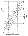
- the graph 65 in FIG. 4 illustrates the typical relationship (calculated) between size, realized gain, and frequency for a single hexagonal passive loop antenna.
- the graph 65 in FIG. 4 also illustrates the typical realized gain provided by an embodiment of the antenna assembly.
- the antenna assembly corresponding to the graph 65 is a single passive loop antenna similar to the antenna assembly 20 in FIG. 1 , and is copper and greater than 3 RF skin depths thick.
- the antenna assembly is tuned and matched, by using radiation pattern peak gain, for example, and the polarization is co-polarized.
- the lines 66, 67, 68, and 69 correspond to +1.5, 0.0,-10.0, and -20.0 dBil realized gain, respectively.
- the embodiments advantageously allowing tradeoffs between antenna size and realized gain and provide increased efficiency with respect to size.
- GPS Global Positioning System
- the antenna assembly provided relatively high GPS satellite constellation availability so many satellites could be received at once.
- a performance summary for the prototype antenna assembly GPS reception is a follows: GPS Prototype Performance Summary Parameter Value/Function Basis Function Receive antenna for the Global Positioning System (GPS) L1 signal Specified Wireless communications circuitry Battery powered radiolocation tag Implemented Center Frequency GPS L1 at 1575.2 MHz Measured Antenna assembly size Circular disc, 0.900 inches diameter, 0.011 inches thick Measured Number of passive loop antennas One (1) Implemented Outer diameter of passive loop antenna 0.900 inches (0.12 ⁇ ) Measured Outer diameter of active loop antenna 0.306 inches Measured PWB Material 0.010 inch thick G10 epoxy glass with 1 ⁇ 2 ounce copper conductors Specified Copper trace thickness 0.0007 inches Nominal Passive loop antenna trace width 0.19 inches Measured Active loop antenna trace width 0.0
- the GPS prototype had the operative advantage of reduced deep cross sense circular polarization fades.
- Right hand circularly polarized microstrip patch antennas tend to become left hand circularly polarized when inverted, which can produce deep fades in GPS reception.
- wireless communications circuitry includes a GPS radiolocation tag, for example, with an antenna assembly
- the antenna assembly provided increased reliability reception than a microstrip patch antenna having circular polarization and higher gain, for example.
- the antenna is generally un-aimed and unoriented. Indeed, in the present embodiment, when the circumference of the passive loop antenna approaches 1 ⁇ 2 wavelength, the radiation pattern becomes nearly spherical and isotropic.
- the circuit equivalent model of the antenna assembly 20 may be regarded as a transformer with multiple secondary windings, so that a power divider is realized, for example.
- the signal generator S corresponds to the wireless communications circuitry 12.
- the active loop antenna 23 corresponds to a primary winding L
- the three hexagonal passive loop antennas 22a-22c correspond to respective secondaries k 1 , k 2 , k 3 .
- Power may be equally divided three-ways, by the active loop antenna 23 being concentric with the center point 24 defined by the three hexagonal passive loop antennas 22a-22c. Adjustment of the amount of coextension of the three hexagonal passive loop antennas 22a-22c over the active loop antenna 23 is equivalent to adjustment of the "turns ratio" of conventional transformers having multiple turn windings.
- the equivalent tuning elements are the capacitors C 1 , C 2 , C 3 .
- the illustrated resistors R r1 , R r2 , R r3 correspond to the radiation resistance. In other words, this is the resistance provided by the conductor itself, for example, a copper conductor.
- R 11 , R 12 , R 13 correspond to conductor resistance loss from joule effect heating.
- R 1 is usually the predominant determinant of the antenna efficiency. In fact, tuning capacitor equivalent series resistance (ESR) losses often may be neglected.
- the loss resistance of metal conductors is generally a fundamental limitation to efficiency and gain of room temperature electrically small antennas.
- the directivity of an individual passive loop antenna is 1.76 dB. This value of directivity does not significantly increase or decrease with the number or passive loop antennas.
- the active loop antenna may be adjusted to provide 50 ohms of resistance, and the metal conductor loss of the active loop may be neglected.
- the passive loop antennas typically do not significantly couple to one another when their loop structures do not overlap, e.g., the mutual coupling is less than about -15 dB in those circumstances. Overlapping of the passive loop antennas may alter the mutual coupling as desired. The degree of mutual coupling adjusts the spacing between the Chebyschev responses.
- the features of the present embodiments allow for control of driving resistance (active loop diameter), reactance (tuning capacitor), frequency (tuning element value), element mutual coupling (spacing between passive loop antennas, size (tuning element provides loading), gain (passive loop antenna diameter), and bandwidth (the number of passive loop antennas 22 adjust the frequency response ripple).
- an antenna assembly 20' illustratively includes four passive loop antennas 22a'-22d' each having a square shape and carried by a first side 37' of the substrate 21'.
- the four passive loop antennas 22a'-22d' are illustratively arranged in side-by-side relation and define a center point 24' corresponding to a corner of each of the square passive loop antennas.
- the active loop antenna 23' which is carried on a second side 38' of the substrate 21', or opposite side from the passive loop antennas 22', is partially coextensive with each of the four square shaped passive loop antennas 22a'-22d'.
- Each of the four square passive loop antennas 22a'-22d' includes a respective tuning member 28a'-28d', or capacitor coupled to respective passive loop conductors 27a'- 27d'.
- each of the four passive loop antennas 22a'-22d' corresponds to a frequency band that is determined by respective capacitors 28a'-28d'.
- yet another embodiment of the antenna assembly 20" illustratively includes eight passive loop antennas 22a"-22h” each having a triangular or pie shape.
- the eight passive loop antennas 22a"-22h” are illustratively arranged in side-by-side relation and define a center point 24" corresponding to a point of each of the triangular passive loop antennas.
- the active loop antenna 23" is partially coextensive with each of the eight triangular shaped passive loop antennas 22a"-22h".
- Each of the eight triangular passive loop antennas 22a"-22" includes a respective tuning member 28a'-28d', or capacitor, coupled to respective passive loop conductors 27a"-27h".
- each of the eight passive loop antennas 27a"-27h" corresponds to a frequency band that is determined by respective capacitors 28a"-28h”.
- each passive loop antenna 22 described herein is illustratively a same size shape, the passive loop antennas may have any polygonal shape. Additionally, in some embodiments, each of the passive loop antennas 22 may not be the same size.
- a method aspect is directed to a method of making an antenna assembly 20 to be carried by a housing 11 and to be coupled to wireless communications circuitry 12.
- the method includes positioning a plurality of passive loop antennas 22 to be carried by a substrate 21 in side-by-side relation.
- Each of the passive loop antennas 22 include a passive loop conductor 27 and a tuning element 28 coupled thereto.
- the method also includes positioning an active loop antenna 23 to be carried by the substrate 21 and to be at least partially coextensive with each of the passive loop antennas 22.
- the active loop antenna 23 includes an active loop conductor 25 and a pair of feedpoints 26a, 26b, defined therein.
- the gain response of a double tuned / 4 th order Chebyschev embodiment of the antenna assembly is illustrated.
- a rippled passband 106 with two gain peaks, but the two peaks of passband are considered as being a single continuous passband, e.g., so a single band antenna with ripple is formed.
- Ripple in the passband 106 may be particularly beneficial to provide increased bandwidth, for example.
- the antenna assembly corresponding to the graph 100 includes two (2) passive loop antennas are adjacent each other with one (1) active loop antenna overlapping each passive loop antenna.
- the radiating loop antennas are preferentially of equal size, and they use similar or identical value tuning element capacitors.
- the individual resonant frequencies of the passive loop antennas are the same by themselves.
- mutual coupling may cause the two gain peaks 106, 108 in the frequency response to form.
- the quadratic responses of two individual passive loop antennas thus combine to become a double tuned 4 th order Chebyschev response.
- the ripple amplitude 104 and the bandwidth 106 may be adjusted by adjusting the spacing of the passive loop antennas with respect to each other. When the two passive loop antennas are further apart, the spacing between gain peaks 102 is reduced and so the bandwidth 106 is reduced, and the ripple level amplitude 104 is reduced.
- the spacing between the two passive loop antennas are closer, the spacing 102 between the gain peaks 108, 110 is increased (the responses spread apart), so the bandwidth 106 is increased, and the ripple amplitude 104 is increased.
- the two passive loop antennas may even overlap each other (but not touch each other) to create relatively very large bandwidths.
- the double tuned 4 th order Chebyschev embodiment advantageously provides a wide and continuous range of tradeoff between ripple level 104 and bandwidth 106.
- the diameter of the active loop antenna adjusts the circuit resistance that the antenna provides to the wireless communications circuitry.
- a larger diameter active loop increases the resistance provided to the transmitter, and a smaller diameter active loop reduces the resistance provided to the transmitter.
- Fifty ohms resistance has been readily achievable in practice when the diameter of the active loop was about 0.2 to 0.5 the diameter of a passive loop antennas.
- the size of the active loop antenna may be adjusted to obtain active and 1 to 1 VSWR. Alternatively, the active loop antenna may be increased in size to provide an overactive trade for increased bandwidth with increased VSWR at the two gain peaks 108, 110.
- the active loop antenna advantageously provides a resistance compensation over a given frequency.
- the passive loop antennas become smaller, their radiation resistance drops, but the the coupling factor of the active loop antenna increases as the passive loop antennas become smaller.
- the desired resistance seen by the electronics circuitry may be constant over a relatively broad bandwidth.
- the compensation behavior is thought to be due to the transition in the passive loop antennas' current distribution from sinusoidal to uniform with reduced passive loop antenna circumference. Loop antennas have stronger magnetic near fields when electrically small so they become better transformer secondaries.
- the passive loop antenna is a far field antenna for radiation, and also a near field antenna.
- the electrical conductor forming the passive loop antennas have a width near 0.15 that of the loop outer diameter.
- the passive loop antenna has an outside diameter of 1.0 inch, and each passive loop antenna is wire, the highest realized gain typically occur when the wire diameter is 0.15 inches.
- the passive loop antenna is 1 inch in diameter and formed as a printed wiring board (PWB) trace, the width of that trace should be also about 0.15 inches for increased radiation efficiency.
- PWB printed wiring board
- the conductor loss resistance is increased when the trace width is too small as there is too little metal to conduct efficiently. Yet, when the trace width is too large, proximity effect increases the conductor loss resistance. When conductor proximity effect occurs, the current hugs the inside edge of the loop conductor and not all the metal is put used for radiating. The loop conductor on the opposite side of the loop causes the proximity effect. The hole in the loop should generally be sized appropriately. The optimal loop conductor trace width for the passive loop antennas was verified by experiment.
- the graph 110 of FIG. 9 illustrates the measured quality factor (Q) 111 of a PWB embodiment single passive loop antenna versus loop conductor trace width.
- Q is an indication of antenna gain so when the Q is highest the realized antenna gain is highest.
- the outer loop diameter was 1.0 inch and it was operated at 146.52 MHz so the outer loop diameter was ⁇ /84. Thus, critical active and resonance at 146.52 MHz was considered and adjusted.
- the thickness of the PWB copper traces was greater than 3 skin depths thick. When the loop antenna hole was 90 percent of the outer diameter, a 22 picofarad capacitor was connected across a gap in the loop to cause set the resonance at 146.52 MHz. When the passive loop antenna internal hole size was zero, the antenna was effectively a notched metal disc.
- the active loop antenna 23 typically does not radiate appreciably or have significant ohmic losses. As background, the active loop antenna 23 also provides a balun of the isolation transformer type.
- the antenna assembly 20 accomplishes this operative advantage by having stronger radial magnetic near fields rather than radial electric near fields which minimizes PWB dielectric losses.
- the antenna assembly 20 tuning and loading is accomplished by component capacitors rather than the PWB dielectric.
- chip capacitors are relatively inexpensive and low loss, and the NPO variety has relatively flat temperature coefficients. Stable capacitance over temperature means that the antenna assembly 20 can have relatively stable frequency of operation over temperature. This can be an advantage of the antenna assembly 20 over typical microstrip patch antennas, for example.
- microstrip patch antennas may require costly, low loss controlled permittivity materials as the antenna "patch" forms a printed circuit transmission line concentrating electric near fields in the PWB dialectic.
- the capacitance of microstrip patch antenna PWB materials is generally not as stable over temperature as are NPO chip capacitors.
- antenna 20 may have stable tuning along and may be planar and relatively easy to construct at a relatively low expense.
- inventions advantageously provide multi-band operation and/or to provide relatively broad single band bandwidth with a Chebyschev passband response.
- embodiments of the antenna assembly also provide broad tunable bandwidth.
- Variable tuning over a wide range is accomplished by varying the reactance of a tuning element 28, for example.
- the tuning element 28 may be a variable capacitor, for example.
- the tunable bandwidth can be over a 7 to 1 frequency range with a relatively low voltage standing wave ratio (VSWR).
- VSWR voltage standing wave ratio
- a VSWR under 2 to 1 was realized across a continuous 3 to 22 MHz tuning range using a vacuum variable capacitor having a range of 10 to 1000 picofarads, and the passive loop antenna 22 was formed from a hexagon of copper water pipe having a circumference of 18 feet.
- the tuning element 28 may be a varactor diode for electronic tuning, for example.
- the desired value of the tuning element 28 may be calculated from the common resonance formula 1/2 ⁇ LC once the inductance of the passive loop antenna 22 is known.
- the antenna assembly 20 is for television and FM broadcast reception with extended range. Typical broadcasts in these frequency bands include horizontal polarization components, and the antenna assembly 20 advantageously responds to horizontal polarization components when oriented in the horizontal plane. Horizontal polarization is known to propagate over the horizon by tropospheric refraction. Thus, the antenna assembly 20 may provide greater range than a vertical 1 ⁇ 2 wave dipole.
- the antenna assembly 20 is omni-directional when horizontally polarized, aiming may not be desired.
- a passive loop antenna 22a-22c can render +1.0 dBil realized gain at 100 MHz when it is 19 inches in diameter, and thus may be used indoors.
- loop antennas and dipole antennas Although there are many differences between loop antennas and dipole antennas, electrically small dipole antennas and loop antennas are typically loaded to smaller size with capacitors and inductors respectively. In the current art, and at room temperature, there are better insulators than conductors, so the efficiency and Q of capacitors is usually much better than inductors. Indeed, the quality factor of capacitors is typically 10 to 100 times better than inductors.
- loop antennas similar to the present embodiments of the antenna assembly may be preferred over dipole antennas as they may accomplish size reduction, loading, and tuning using relatively low loss and relatively inexpensive capacitors. Loop antennas also provide an inductor and a transformer winding with limited or reduced additional components.
- the present embodiments provide a compound design in which the antenna inductor, matching transformer, and balun are integrated into the antenna structure.
Landscapes
- Engineering & Computer Science (AREA)
- Computer Networks & Wireless Communication (AREA)
- Variable-Direction Aerials And Aerial Arrays (AREA)
- Details Of Aerials (AREA)
Claims (8)
- Drahtlose Kommunikationsvorrichtung (10) mit:- einem Gehäuse (11),- einer drahtlosen Kommunikationsschaltung (12), die von dem Gehäuse (11) getragen wird, und- einer Antennenanordnung (20), die von dem Gehäuse (11) getragen wird und mit der drahtlosen Kommunikationsschaltung (12) gekoppelt ist und umfasst:- ein Substrat (21),- eine Mehrzahl passiver Rahmenantennen (22a-22c), die von dem Substrat (21) getragen werden und nebeneinander angeordnet sind, wobei jede der Mehrzahl passiver Rahmenantennen (22a-22c) einen passiven Schleifenleiter (27a-27c) und ein damit gekoppeltes Abstimmelement (28) umfasst, wobei jede der Mehrzahl passiver Rahmenantennen (22a-22c) eine jeweilige an jede benachbarte passive Antenne angrenzende gerade Seite aufweist, und jede der Mehrzahl passiver Rahmenantennen (22a-22c) eine Länge hat, die kleiner oder gleich 0,5 Wellenlängen bei einer Betriebsfrequenz ist, und- eine aktive Rahmenantenne (23), die von dem Substrat (21) getragen wird und so angeordnet ist, dass sie zumindest teilweise mit jeder der Mehrzahl passiver Rahmenantennen (22a-22c) koextensiv ist, wobei die aktive Rahmenantenne (23) einen aktiven Schleifenleiter (25) und ein Paar darin ausgebildeter Speisepunkte (26a, 26b) umfasst.
- Drahtlose Kommunikationsvorrichtung nach Anspruch 1, wobei jede der Mehrzahl passiver Rahmenantennen (22a-22c) eine polygonale Gestalt hat.
- Drahtlose Kommunikationsvorrichtung nach Anspruch 2, wobei die polygonale Gestalt eine viereckige Gestalt, eine sechseckige Gestalt oder eine dreieckige Gestalt ist.
- Drahtlose Kommunikationsvorrichtung nach Anspruch 1, wobei jede der Mehrzahl passiver Rahmenantennen (22a-22c) dieselbe Größe und Gestalt hat.
- Drahtlose Kommunikationsvorrichtung nach Anspruch 1, wobei die aktive Rahmenantenne (23) eine kreisförmige Gestalt hat.
- Verfahren zum Herstellen einer von einem Gehäuse (11) zu tragenden und mit einer drahtlosen Kommunikationsschaltung (12) zu koppelnden Antennenanordnung (20), wobei das Verfahren umfasst:- Positionieren einer nebeneinander von einem Substrat (21) zu tragenden Mehrzahl passiver Rahmenantennen (22a-22c), wobei jede der Mehrzahl passiver Rahmenantennen (22a-22c) so positioniert wird, dass eine jeweilige gerade Seite an jede benachbarte passive Antenne (22a-22c) angrenzt, wobei jede der Mehrzahl passiver Rahmenantennen (22a-22c) einen passiven Schleifenleiter (27a-27c) und ein damit gekoppeltes Abstimmelement (28) umfasst, und jede der Mehrzahl passiver Rahmenantennen (22a-22c) eine Länge hat, die kleiner oder gleich 0,5 Wellenlängen einer bei Betriebsfrequenz ist, und- Positionieren einer von dem Substrat (21) zu tragenden und so anzuordnenden aktiven Rahmenantenne (23), dass sie zumindest teilweise mit jeder der Mehrzahl passiver Rahmenantennen (22a-22c) koextensiv ist, wobei die aktive Rahmenantenne (23) einen aktiven Schleifenleiter (25) und ein Paar darin ausgebildeter Speisepunkte (26a, 26b) umfasst.
- Verfahren nach Anspruch 6, wobei jede der Mehrzahl passiver Rahmenantennen (22a-22c) eine polygonale Gestalt hat.
- Verfahren nach Anspruch 6, wobei die aktive Rahmenantenne (23) eine kreisförmige Gestalt hat.
Applications Claiming Priority (2)
| Application Number | Priority Date | Filing Date | Title |
|---|---|---|---|
| US13/076,587 US8982008B2 (en) | 2011-03-31 | 2011-03-31 | Wireless communications device including side-by-side passive loop antennas and related methods |
| PCT/US2012/027609 WO2012134709A1 (en) | 2011-03-31 | 2012-03-02 | Wireless communications device including side-by-side passive loop antennas and related methods |
Publications (2)
| Publication Number | Publication Date |
|---|---|
| EP2692016A1 EP2692016A1 (de) | 2014-02-05 |
| EP2692016B1 true EP2692016B1 (de) | 2015-08-12 |
Family
ID=45895462
Family Applications (1)
| Application Number | Title | Priority Date | Filing Date |
|---|---|---|---|
| EP12711292.8A Active EP2692016B1 (de) | 2011-03-31 | 2012-03-02 | Drahtlose kommunikationsvorrichtung mit passiven nebeneinander angeordnenten rahmenantennen und zugehörige verfahren |
Country Status (7)
| Country | Link |
|---|---|
| US (1) | US8982008B2 (de) |
| EP (1) | EP2692016B1 (de) |
| JP (1) | JP2014509815A (de) |
| KR (1) | KR101569979B1 (de) |
| CN (1) | CN103477496B (de) |
| TW (1) | TWI521801B (de) |
| WO (1) | WO2012134709A1 (de) |
Families Citing this family (69)
| Publication number | Priority date | Publication date | Assignee | Title |
|---|---|---|---|---|
| US9232893B2 (en) | 2009-03-09 | 2016-01-12 | Nucurrent, Inc. | Method of operation of a multi-layer-multi-turn structure for high efficiency wireless communication |
| US9444213B2 (en) | 2009-03-09 | 2016-09-13 | Nucurrent, Inc. | Method for manufacture of multi-layer wire structure for high efficiency wireless communication |
| US9300046B2 (en) | 2009-03-09 | 2016-03-29 | Nucurrent, Inc. | Method for manufacture of multi-layer-multi-turn high efficiency inductors |
| US9439287B2 (en) | 2009-03-09 | 2016-09-06 | Nucurrent, Inc. | Multi-layer wire structure for high efficiency wireless communication |
| US9208942B2 (en) * | 2009-03-09 | 2015-12-08 | Nucurrent, Inc. | Multi-layer-multi-turn structure for high efficiency wireless communication |
| US11476566B2 (en) | 2009-03-09 | 2022-10-18 | Nucurrent, Inc. | Multi-layer-multi-turn structure for high efficiency wireless communication |
| US9306358B2 (en) | 2009-03-09 | 2016-04-05 | Nucurrent, Inc. | Method for manufacture of multi-layer wire structure for high efficiency wireless communication |
| US20120268346A1 (en) * | 2011-04-25 | 2012-10-25 | Lockheed Martin Corporation | Biologically inspired beam forming small antenna arrays |
| FR2988195B1 (fr) | 2012-03-14 | 2015-04-10 | Continental Automotive France | Dispositif de detection et de communication en champ proche |
| WO2014088323A1 (en) * | 2012-12-04 | 2014-06-12 | Samsung Electronics Co., Ltd. | Antenna for wireless power transmission and near field communication |
| US9281118B2 (en) * | 2012-12-10 | 2016-03-08 | Intel Corporation | Cascaded coils for multi-surface coverage in near field communication |
| EP3579338A1 (de) * | 2013-03-06 | 2019-12-11 | NuCurrent, Inc. | Mehrlagige drahtstruktur für hochwirksame drahtloskommunikation |
| US9847576B2 (en) * | 2013-11-11 | 2017-12-19 | Nxp B.V. | UHF-RFID antenna for point of sales application |
| EP3068299B1 (de) * | 2013-11-14 | 2019-05-08 | Technische Universiteit Eindhoven | System zur ortung eines objekts unter verwendung einer antennengruppe mit teilweise überlappenden spulen |
| TWI509891B (zh) * | 2013-11-22 | 2015-11-21 | Wistron Neweb Corp | 迴圈天線 |
| US9306283B2 (en) | 2014-01-24 | 2016-04-05 | Sony Corporation | Antenna device and method for increasing loop antenna communication range |
| KR101584764B1 (ko) * | 2014-04-17 | 2016-01-12 | 주식회사 이엠따블유 | 다중 안테나 |
| FR3024594B1 (fr) | 2014-07-31 | 2017-12-01 | Continental Automotive France | Dispositif de communication radiofrequence en champ proche avec un element portable embarque dans un vehicule automobile |
| CN104157980B (zh) * | 2014-08-08 | 2017-02-15 | 电子科技大学 | 可重构微带八木天线 |
| US9735822B1 (en) * | 2014-09-16 | 2017-08-15 | Amazon Technologies, Inc. | Low specific absorption rate dual-band antenna structure |
| CN104362432A (zh) * | 2014-11-13 | 2015-02-18 | 杭州立方控股股份有限公司 | 一种印刷螺旋天线的制作方法 |
| CN109786964B (zh) * | 2014-11-18 | 2023-11-03 | 康普技术有限责任公司 | 用于多频带辐射阵列的掩蔽的低频带元件 |
| US10056689B2 (en) | 2015-06-09 | 2018-08-21 | Electronics And Telecommunications Research Institute | Electronically steerable parasitic radiator antenna and beam forming apparatus |
| US10063100B2 (en) | 2015-08-07 | 2018-08-28 | Nucurrent, Inc. | Electrical system incorporating a single structure multimode antenna for wireless power transmission using magnetic field coupling |
| US9941729B2 (en) | 2015-08-07 | 2018-04-10 | Nucurrent, Inc. | Single layer multi mode antenna for wireless power transmission using magnetic field coupling |
| US9960628B2 (en) | 2015-08-07 | 2018-05-01 | Nucurrent, Inc. | Single structure multi mode antenna having a single layer structure with coils on opposing sides for wireless power transmission using magnetic field coupling |
| US9941743B2 (en) | 2015-08-07 | 2018-04-10 | Nucurrent, Inc. | Single structure multi mode antenna having a unitary body construction for wireless power transmission using magnetic field coupling |
| US9941590B2 (en) | 2015-08-07 | 2018-04-10 | Nucurrent, Inc. | Single structure multi mode antenna for wireless power transmission using magnetic field coupling having magnetic shielding |
| US11205848B2 (en) | 2015-08-07 | 2021-12-21 | Nucurrent, Inc. | Method of providing a single structure multi mode antenna having a unitary body construction for wireless power transmission using magnetic field coupling |
| US9948129B2 (en) | 2015-08-07 | 2018-04-17 | Nucurrent, Inc. | Single structure multi mode antenna for wireless power transmission using magnetic field coupling having an internal switch circuit |
| US10658847B2 (en) | 2015-08-07 | 2020-05-19 | Nucurrent, Inc. | Method of providing a single structure multi mode antenna for wireless power transmission using magnetic field coupling |
| US10636563B2 (en) | 2015-08-07 | 2020-04-28 | Nucurrent, Inc. | Method of fabricating a single structure multi mode antenna for wireless power transmission using magnetic field coupling |
| US9960629B2 (en) | 2015-08-07 | 2018-05-01 | Nucurrent, Inc. | Method of operating a single structure multi mode antenna for wireless power transmission using magnetic field coupling |
| WO2017031348A1 (en) | 2015-08-19 | 2017-02-23 | Nucurrent, Inc. | Multi-mode wireless antenna configurations |
| USD827620S1 (en) | 2015-10-08 | 2018-09-04 | Antennas Direct, Inc. | Antenna element |
| US10128575B2 (en) | 2015-09-02 | 2018-11-13 | Antennas Direct, Inc. | HDTV antenna assemblies |
| USD824884S1 (en) | 2015-10-08 | 2018-08-07 | Antennas Direct, Inc. | Antenna element |
| US9761935B2 (en) * | 2015-09-02 | 2017-09-12 | Antennas Direct, Inc. | HDTV antenna assemblies |
| USD811752S1 (en) | 2015-10-08 | 2018-03-06 | Antennas Direct, Inc. | Picture frame antenna |
| TWI584713B (zh) * | 2015-10-29 | 2017-05-21 | Huang-Chieh Metal Composite Material Tech Co Ltd | The structure of a metal housing of a radio wave communication device and a method of manufacturing the same |
| US10714960B2 (en) * | 2015-12-22 | 2020-07-14 | Intel Corporation | Uniform wireless charging device |
| TWI629835B (zh) | 2016-07-21 | 2018-07-11 | 和碩聯合科技股份有限公司 | 天線單元、天線系統及天線控制方法 |
| CN109804516B (zh) | 2016-08-26 | 2021-11-02 | 纽卡润特有限公司 | 无线连接器系统 |
| US10601468B2 (en) * | 2016-09-06 | 2020-03-24 | Apple Inc. | Wirelessly charged devices |
| CN209590845U (zh) * | 2016-12-02 | 2019-11-05 | 株式会社村田制作所 | 辅助天线、rfid系统 |
| WO2018107037A1 (en) | 2016-12-09 | 2018-06-14 | Nucurrent, Inc. | A substrate configured to facilitate through-metal energy transfer via near field magnetic coupling |
| US11223234B2 (en) | 2017-02-13 | 2022-01-11 | Nucurrent, Inc. | Method of operating a wireless electrical energy transmission base |
| US11277028B2 (en) | 2017-05-26 | 2022-03-15 | Nucurrent, Inc. | Wireless electrical energy transmission system for flexible device orientation |
| CN107394396B (zh) * | 2017-07-07 | 2020-05-01 | 中国计量科学研究院 | 天线系数可计算的标准环天线、系统及天线系数确定方法 |
| US10811761B2 (en) * | 2018-10-01 | 2020-10-20 | Auden Techno Corp. | Information carrier and tag antenna structure thereof |
| JP7169897B2 (ja) * | 2019-02-12 | 2022-11-11 | 株式会社日立製作所 | 受電ユニット、送電ユニット及び無線給電装置 |
| TWI699042B (zh) * | 2019-06-28 | 2020-07-11 | 啓碁科技股份有限公司 | 天線結構 |
| US11271430B2 (en) | 2019-07-19 | 2022-03-08 | Nucurrent, Inc. | Wireless power transfer system with extended wireless charging range |
| US11227712B2 (en) | 2019-07-19 | 2022-01-18 | Nucurrent, Inc. | Preemptive thermal mitigation for wireless power systems |
| US11056922B1 (en) | 2020-01-03 | 2021-07-06 | Nucurrent, Inc. | Wireless power transfer system for simultaneous transfer to multiple devices |
| ES2982188T3 (es) * | 2020-01-23 | 2024-10-15 | Premo Sl | Antena universal tridimensional multibanda |
| CN111725610B (zh) * | 2020-06-30 | 2022-05-10 | 西安易朴通讯技术有限公司 | 一种双环天线、天线模组及移动终端 |
| US11283303B2 (en) | 2020-07-24 | 2022-03-22 | Nucurrent, Inc. | Area-apportioned wireless power antenna for maximized charging volume |
| CN112436269B (zh) * | 2020-11-16 | 2022-07-05 | 重庆大学 | 一种频率捷变方向图可重构的惠更斯源电小天线 |
| KR20220075956A (ko) | 2020-11-30 | 2022-06-08 | 현대자동차주식회사 | 메타 물질 전자파 흡수체 |
| US11881716B2 (en) | 2020-12-22 | 2024-01-23 | Nucurrent, Inc. | Ruggedized communication for wireless power systems in multi-device environments |
| US11876386B2 (en) | 2020-12-22 | 2024-01-16 | Nucurrent, Inc. | Detection of foreign objects in large charging volume applications |
| US12009915B2 (en) | 2021-01-29 | 2024-06-11 | Eagle Technology, Llc | Compact receiver system with antijam and antispoof capability |
| US11502414B2 (en) | 2021-01-29 | 2022-11-15 | Eagle Technology, Llc | Microstrip patch antenna system having adjustable radiation pattern shapes and related method |
| US11695302B2 (en) | 2021-02-01 | 2023-07-04 | Nucurrent, Inc. | Segmented shielding for wide area wireless power transmitter |
| US11942698B2 (en) * | 2021-03-19 | 2024-03-26 | City University Of Hong Kong | Electrically small, planar, horizontally polarized dual-band omnidirectional antenna |
| US12133314B2 (en) | 2021-04-13 | 2024-10-29 | Apple Inc. | Electronic devices having failsafe mechanisms with near field communications |
| US12003116B2 (en) | 2022-03-01 | 2024-06-04 | Nucurrent, Inc. | Wireless power transfer system for simultaneous transfer to multiple devices with cross talk and interference mitigation |
| US11831174B2 (en) | 2022-03-01 | 2023-11-28 | Nucurrent, Inc. | Cross talk and interference mitigation in dual wireless power transmitter |
Family Cites Families (23)
| Publication number | Priority date | Publication date | Assignee | Title |
|---|---|---|---|---|
| SE9700401D0 (sv) * | 1997-02-05 | 1997-02-05 | Allgon Ab | Antenna operating with isolated channels |
| WO1999013528A1 (en) | 1997-09-10 | 1999-03-18 | Rangestar International Corporation | Loop antenna assembly for telecommunications devices |
| US6570541B2 (en) | 1998-05-18 | 2003-05-27 | Db Tag, Inc. | Systems and methods for wirelessly projecting power using multiple in-phase current loops |
| US6427913B1 (en) * | 1998-09-11 | 2002-08-06 | Key-Trak, Inc. | Object control and tracking system with zonal transition detection |
| JP2001244727A (ja) * | 2000-03-02 | 2001-09-07 | Nippon Dengyo Kosaku Co Ltd | マイクロストリップアンテナ |
| US6781552B2 (en) | 2002-11-22 | 2004-08-24 | Quanta Computer Inc. | Built-in multi-band mobile phone antenna assembly with coplanar patch antenna and loop antenna |
| US6788261B1 (en) * | 2003-04-09 | 2004-09-07 | Wilson Electronics, Inc. | Antenna with multiple radiators |
| US6992630B2 (en) | 2003-10-28 | 2006-01-31 | Harris Corporation | Annular ring antenna |
| US7432874B2 (en) | 2004-07-22 | 2008-10-07 | Feig Electronic Gmbh | Antenna array |
| WO2006033408A1 (ja) | 2004-09-22 | 2006-03-30 | Matsushita Electric Industrial Co., Ltd. | ループアンテナユニット及び無線通信媒体処理装置 |
| JP4521724B2 (ja) | 2005-01-20 | 2010-08-11 | ソニー・エリクソン・モバイルコミュニケーションズ株式会社 | アンテナ装置及びこのアンテナ装置を備えた携帯端末装置 |
| US7268742B2 (en) | 2005-03-22 | 2007-09-11 | Mobile Aspects, Inc. | Antenna arrangement |
| JP2006340246A (ja) | 2005-06-06 | 2006-12-14 | Toyota Central Res & Dev Lab Inc | アンテナ装置 |
| US7374105B2 (en) * | 2005-10-29 | 2008-05-20 | Magnex Corporation | RFID tag with improved range |
| US8219143B2 (en) * | 2006-09-28 | 2012-07-10 | Kyocera Corporation | Mobile radio device |
| DE102007026965A1 (de) | 2007-06-12 | 2009-01-02 | Siemens Ag | Antennenarray |
| CA2660357C (en) * | 2007-08-23 | 2016-03-01 | Mallinckrodt Inc. | Syringe content detection using rf energy |
| DE102007052446B4 (de) | 2007-11-02 | 2010-02-11 | Siemens Ag | Kopfspule für ein Magnetresonanzgerät und Verwendung einer Kopfspule in der Magnetresonanz-Tomographie |
| DE102008011144B4 (de) | 2008-02-26 | 2012-02-16 | Siemens Aktiengesellschaft | Antennenanordnung für ein Magnetresonanzgerät |
| WO2011044383A1 (en) * | 2009-10-08 | 2011-04-14 | Checkpoint Systems, Inc. | Security tag utilizing two rfid reflectivity modes |
| AU2010315240B2 (en) * | 2009-11-04 | 2016-05-05 | Allflex USA LLC | Signal cancelling transmit/receive multi-loop antenna for a radio frequency identification reader |
| US8587407B2 (en) * | 2010-12-06 | 2013-11-19 | Ncr Corporation | Media transaction kiosk and method |
| US9579510B2 (en) * | 2011-07-19 | 2017-02-28 | Cochlear Limited | Implantable remote control |
-
2011
- 2011-03-31 US US13/076,587 patent/US8982008B2/en active Active
-
2012
- 2012-03-02 JP JP2014502582A patent/JP2014509815A/ja active Pending
- 2012-03-02 WO PCT/US2012/027609 patent/WO2012134709A1/en not_active Ceased
- 2012-03-02 KR KR1020137026727A patent/KR101569979B1/ko not_active Expired - Fee Related
- 2012-03-02 EP EP12711292.8A patent/EP2692016B1/de active Active
- 2012-03-02 CN CN201280015526.6A patent/CN103477496B/zh not_active Expired - Fee Related
- 2012-03-20 TW TW101109558A patent/TWI521801B/zh not_active IP Right Cessation
Also Published As
| Publication number | Publication date |
|---|---|
| JP2014509815A (ja) | 2014-04-21 |
| CN103477496A (zh) | 2013-12-25 |
| TWI521801B (zh) | 2016-02-11 |
| EP2692016A1 (de) | 2014-02-05 |
| KR20140026401A (ko) | 2014-03-05 |
| KR101569979B1 (ko) | 2015-11-17 |
| TW201242170A (en) | 2012-10-16 |
| US8982008B2 (en) | 2015-03-17 |
| CN103477496B (zh) | 2015-09-02 |
| WO2012134709A1 (en) | 2012-10-04 |
| US20120249396A1 (en) | 2012-10-04 |
Similar Documents
| Publication | Publication Date | Title |
|---|---|---|
| EP2692016B1 (de) | Drahtlose kommunikationsvorrichtung mit passiven nebeneinander angeordnenten rahmenantennen und zugehörige verfahren | |
| Cai et al. | Compact-size low-profile wideband circularly polarized omnidirectional patch antenna with reconfigurable polarizations | |
| AU760084B2 (en) | Circularly polarized dielectric resonator antenna | |
| US8164529B2 (en) | Loop antenna including impedance tuning gap and associated methods | |
| KR101226867B1 (ko) | 하프-루프 칩 안테나 및 연관 방법 | |
| EP2504885B1 (de) | Kommunikationsflachantenne mit epizyklischer struktur und isotroper strahlung sowie zugehörige verfahren | |
| USRE40129E1 (en) | Wide bandwidth multi-mode antenna | |
| US20150102972A1 (en) | Method and apparatus for high-performance compact volumetric antenna with pattern control | |
| Chen | A compact wideband filtering omnidirectional dipole antenna without extra circuits | |
| US9748654B2 (en) | Antenna systems with proximity coupled annular rectangular patches | |
| Wang et al. | Low-profile omnidirectional WIFI antennas with pattern reconfigurability inspired by meta-resonators | |
| CA2725029A1 (en) | Folded conical antenna and associated methods | |
| CN109216912B (zh) | 一种加载六边形环寄生枝节的花形馈源终端多频微带天线 | |
| Tang et al. | Frequency-agile, efficient, near-field resonant parasitic monopole antenna | |
| US20110006957A1 (en) | Method and apparatus for a high-performance compact volumetric antenna | |
| US6738026B1 (en) | Low profile tri-filar, single feed, helical antenna | |
| Fusco et al. | Quadrifilar loop antenna | |
| Öner et al. | Design of a Compact Multilayer High-Gain Microstrip Patch Antenna for IoT Applications | |
| Sim et al. | A dual‐band antenna design for GPS and UMTS applications | |
| Monica et al. | Quadrifilar Conical Helix-Antenna and Its Radiation Characteristics Evaluation | |
| Sayyad | Design and Simulation of An Octagonal Microstrip Antenna Array | |
| Alibakhshi-Kenari et al. | Compact planar antennas for beam steering and RFID tags | |
| Kumara et al. | A low profile circularly polarized UWB antenna with integrated GSM band for wireless communication | |
| WO2020088760A1 (en) | Turnchip circularly polarized antenna |
Legal Events
| Date | Code | Title | Description |
|---|---|---|---|
| PUAI | Public reference made under article 153(3) epc to a published international application that has entered the european phase |
Free format text: ORIGINAL CODE: 0009012 |
|
| 17P | Request for examination filed |
Effective date: 20131010 |
|
| AK | Designated contracting states |
Kind code of ref document: A1 Designated state(s): AL AT BE BG CH CY CZ DE DK EE ES FI FR GB GR HR HU IE IS IT LI LT LU LV MC MK MT NL NO PL PT RO RS SE SI SK SM TR |
|
| DAX | Request for extension of the european patent (deleted) | ||
| GRAP | Despatch of communication of intention to grant a patent |
Free format text: ORIGINAL CODE: EPIDOSNIGR1 |
|
| RIC1 | Information provided on ipc code assigned before grant |
Ipc: H01Q 21/06 20060101ALI20150128BHEP Ipc: H01Q 1/24 20060101AFI20150128BHEP Ipc: H01Q 7/00 20060101ALI20150128BHEP Ipc: H01Q 5/385 20150101ALI20150128BHEP |
|
| INTG | Intention to grant announced |
Effective date: 20150213 |
|
| GRAS | Grant fee paid |
Free format text: ORIGINAL CODE: EPIDOSNIGR3 |
|
| GRAP | Despatch of communication of intention to grant a patent |
Free format text: ORIGINAL CODE: EPIDOSNIGR1 |
|
| GRAA | (expected) grant |
Free format text: ORIGINAL CODE: 0009210 |
|
| INTG | Intention to grant announced |
Effective date: 20150629 |
|
| AK | Designated contracting states |
Kind code of ref document: B1 Designated state(s): AL AT BE BG CH CY CZ DE DK EE ES FI FR GB GR HR HU IE IS IT LI LT LU LV MC MK MT NL NO PL PT RO RS SE SI SK SM TR |
|
| REG | Reference to a national code |
Ref country code: GB Ref legal event code: FG4D |
|
| REG | Reference to a national code |
Ref country code: CH Ref legal event code: EP |
|
| REG | Reference to a national code |
Ref country code: AT Ref legal event code: REF Ref document number: 742862 Country of ref document: AT Kind code of ref document: T Effective date: 20150815 |
|
| REG | Reference to a national code |
Ref country code: IE Ref legal event code: FG4D |
|
| REG | Reference to a national code |
Ref country code: DE Ref legal event code: R096 Ref document number: 602012009523 Country of ref document: DE |
|
| REG | Reference to a national code |
Ref country code: LT Ref legal event code: MG4D |
|
| REG | Reference to a national code |
Ref country code: AT Ref legal event code: MK05 Ref document number: 742862 Country of ref document: AT Kind code of ref document: T Effective date: 20150812 |
|
| REG | Reference to a national code |
Ref country code: NL Ref legal event code: MP Effective date: 20150812 |
|
| PG25 | Lapsed in a contracting state [announced via postgrant information from national office to epo] |
Ref country code: NO Free format text: LAPSE BECAUSE OF FAILURE TO SUBMIT A TRANSLATION OF THE DESCRIPTION OR TO PAY THE FEE WITHIN THE PRESCRIBED TIME-LIMIT Effective date: 20151112 Ref country code: LV Free format text: LAPSE BECAUSE OF FAILURE TO SUBMIT A TRANSLATION OF THE DESCRIPTION OR TO PAY THE FEE WITHIN THE PRESCRIBED TIME-LIMIT Effective date: 20150812 Ref country code: FI Free format text: LAPSE BECAUSE OF FAILURE TO SUBMIT A TRANSLATION OF THE DESCRIPTION OR TO PAY THE FEE WITHIN THE PRESCRIBED TIME-LIMIT Effective date: 20150812 Ref country code: GR Free format text: LAPSE BECAUSE OF FAILURE TO SUBMIT A TRANSLATION OF THE DESCRIPTION OR TO PAY THE FEE WITHIN THE PRESCRIBED TIME-LIMIT Effective date: 20151113 Ref country code: LT Free format text: LAPSE BECAUSE OF FAILURE TO SUBMIT A TRANSLATION OF THE DESCRIPTION OR TO PAY THE FEE WITHIN THE PRESCRIBED TIME-LIMIT Effective date: 20150812 |
|
| PG25 | Lapsed in a contracting state [announced via postgrant information from national office to epo] |
Ref country code: ES Free format text: LAPSE BECAUSE OF FAILURE TO SUBMIT A TRANSLATION OF THE DESCRIPTION OR TO PAY THE FEE WITHIN THE PRESCRIBED TIME-LIMIT Effective date: 20150812 Ref country code: SE Free format text: LAPSE BECAUSE OF FAILURE TO SUBMIT A TRANSLATION OF THE DESCRIPTION OR TO PAY THE FEE WITHIN THE PRESCRIBED TIME-LIMIT Effective date: 20150812 Ref country code: IS Free format text: LAPSE BECAUSE OF FAILURE TO SUBMIT A TRANSLATION OF THE DESCRIPTION OR TO PAY THE FEE WITHIN THE PRESCRIBED TIME-LIMIT Effective date: 20151212 Ref country code: RS Free format text: LAPSE BECAUSE OF FAILURE TO SUBMIT A TRANSLATION OF THE DESCRIPTION OR TO PAY THE FEE WITHIN THE PRESCRIBED TIME-LIMIT Effective date: 20150812 Ref country code: AT Free format text: LAPSE BECAUSE OF FAILURE TO SUBMIT A TRANSLATION OF THE DESCRIPTION OR TO PAY THE FEE WITHIN THE PRESCRIBED TIME-LIMIT Effective date: 20150812 Ref country code: PL Free format text: LAPSE BECAUSE OF FAILURE TO SUBMIT A TRANSLATION OF THE DESCRIPTION OR TO PAY THE FEE WITHIN THE PRESCRIBED TIME-LIMIT Effective date: 20150812 Ref country code: HR Free format text: LAPSE BECAUSE OF FAILURE TO SUBMIT A TRANSLATION OF THE DESCRIPTION OR TO PAY THE FEE WITHIN THE PRESCRIBED TIME-LIMIT Effective date: 20150812 Ref country code: PT Free format text: LAPSE BECAUSE OF FAILURE TO SUBMIT A TRANSLATION OF THE DESCRIPTION OR TO PAY THE FEE WITHIN THE PRESCRIBED TIME-LIMIT Effective date: 20151214 |
|
| REG | Reference to a national code |
Ref country code: FR Ref legal event code: PLFP Year of fee payment: 5 |
|
| PG25 | Lapsed in a contracting state [announced via postgrant information from national office to epo] |
Ref country code: NL Free format text: LAPSE BECAUSE OF FAILURE TO SUBMIT A TRANSLATION OF THE DESCRIPTION OR TO PAY THE FEE WITHIN THE PRESCRIBED TIME-LIMIT Effective date: 20150812 |
|
| PG25 | Lapsed in a contracting state [announced via postgrant information from national office to epo] |
Ref country code: CZ Free format text: LAPSE BECAUSE OF FAILURE TO SUBMIT A TRANSLATION OF THE DESCRIPTION OR TO PAY THE FEE WITHIN THE PRESCRIBED TIME-LIMIT Effective date: 20150812 Ref country code: SK Free format text: LAPSE BECAUSE OF FAILURE TO SUBMIT A TRANSLATION OF THE DESCRIPTION OR TO PAY THE FEE WITHIN THE PRESCRIBED TIME-LIMIT Effective date: 20150812 Ref country code: IT Free format text: LAPSE BECAUSE OF FAILURE TO SUBMIT A TRANSLATION OF THE DESCRIPTION OR TO PAY THE FEE WITHIN THE PRESCRIBED TIME-LIMIT Effective date: 20150812 Ref country code: EE Free format text: LAPSE BECAUSE OF FAILURE TO SUBMIT A TRANSLATION OF THE DESCRIPTION OR TO PAY THE FEE WITHIN THE PRESCRIBED TIME-LIMIT Effective date: 20150812 Ref country code: DK Free format text: LAPSE BECAUSE OF FAILURE TO SUBMIT A TRANSLATION OF THE DESCRIPTION OR TO PAY THE FEE WITHIN THE PRESCRIBED TIME-LIMIT Effective date: 20150812 |
|
| REG | Reference to a national code |
Ref country code: DE Ref legal event code: R097 Ref document number: 602012009523 Country of ref document: DE |
|
| PG25 | Lapsed in a contracting state [announced via postgrant information from national office to epo] |
Ref country code: RO Free format text: LAPSE BECAUSE OF FAILURE TO SUBMIT A TRANSLATION OF THE DESCRIPTION OR TO PAY THE FEE WITHIN THE PRESCRIBED TIME-LIMIT Effective date: 20150812 |
|
| PLBE | No opposition filed within time limit |
Free format text: ORIGINAL CODE: 0009261 |
|
| STAA | Information on the status of an ep patent application or granted ep patent |
Free format text: STATUS: NO OPPOSITION FILED WITHIN TIME LIMIT |
|
| 26N | No opposition filed |
Effective date: 20160513 |
|
| PG25 | Lapsed in a contracting state [announced via postgrant information from national office to epo] |
Ref country code: SI Free format text: LAPSE BECAUSE OF FAILURE TO SUBMIT A TRANSLATION OF THE DESCRIPTION OR TO PAY THE FEE WITHIN THE PRESCRIBED TIME-LIMIT Effective date: 20150812 Ref country code: BE Free format text: LAPSE BECAUSE OF NON-PAYMENT OF DUE FEES Effective date: 20160331 |
|
| PG25 | Lapsed in a contracting state [announced via postgrant information from national office to epo] |
Ref country code: LU Free format text: LAPSE BECAUSE OF FAILURE TO SUBMIT A TRANSLATION OF THE DESCRIPTION OR TO PAY THE FEE WITHIN THE PRESCRIBED TIME-LIMIT Effective date: 20160302 Ref country code: MC Free format text: LAPSE BECAUSE OF FAILURE TO SUBMIT A TRANSLATION OF THE DESCRIPTION OR TO PAY THE FEE WITHIN THE PRESCRIBED TIME-LIMIT Effective date: 20150812 |
|
| REG | Reference to a national code |
Ref country code: CH Ref legal event code: PL |
|
| REG | Reference to a national code |
Ref country code: IE Ref legal event code: MM4A |
|
| PG25 | Lapsed in a contracting state [announced via postgrant information from national office to epo] |
Ref country code: BE Free format text: LAPSE BECAUSE OF FAILURE TO SUBMIT A TRANSLATION OF THE DESCRIPTION OR TO PAY THE FEE WITHIN THE PRESCRIBED TIME-LIMIT Effective date: 20150812 |
|
| PG25 | Lapsed in a contracting state [announced via postgrant information from national office to epo] |
Ref country code: IE Free format text: LAPSE BECAUSE OF NON-PAYMENT OF DUE FEES Effective date: 20160302 Ref country code: CH Free format text: LAPSE BECAUSE OF NON-PAYMENT OF DUE FEES Effective date: 20160331 Ref country code: LI Free format text: LAPSE BECAUSE OF NON-PAYMENT OF DUE FEES Effective date: 20160331 |
|
| REG | Reference to a national code |
Ref country code: FR Ref legal event code: PLFP Year of fee payment: 6 |
|
| PG25 | Lapsed in a contracting state [announced via postgrant information from national office to epo] |
Ref country code: MT Free format text: LAPSE BECAUSE OF FAILURE TO SUBMIT A TRANSLATION OF THE DESCRIPTION OR TO PAY THE FEE WITHIN THE PRESCRIBED TIME-LIMIT Effective date: 20150812 |
|
| REG | Reference to a national code |
Ref country code: FR Ref legal event code: PLFP Year of fee payment: 7 |
|
| PG25 | Lapsed in a contracting state [announced via postgrant information from national office to epo] |
Ref country code: HU Free format text: LAPSE BECAUSE OF FAILURE TO SUBMIT A TRANSLATION OF THE DESCRIPTION OR TO PAY THE FEE WITHIN THE PRESCRIBED TIME-LIMIT; INVALID AB INITIO Effective date: 20120302 Ref country code: SM Free format text: LAPSE BECAUSE OF FAILURE TO SUBMIT A TRANSLATION OF THE DESCRIPTION OR TO PAY THE FEE WITHIN THE PRESCRIBED TIME-LIMIT Effective date: 20150812 Ref country code: CY Free format text: LAPSE BECAUSE OF FAILURE TO SUBMIT A TRANSLATION OF THE DESCRIPTION OR TO PAY THE FEE WITHIN THE PRESCRIBED TIME-LIMIT Effective date: 20150812 |
|
| PG25 | Lapsed in a contracting state [announced via postgrant information from national office to epo] |
Ref country code: MK Free format text: LAPSE BECAUSE OF FAILURE TO SUBMIT A TRANSLATION OF THE DESCRIPTION OR TO PAY THE FEE WITHIN THE PRESCRIBED TIME-LIMIT Effective date: 20150812 Ref country code: TR Free format text: LAPSE BECAUSE OF FAILURE TO SUBMIT A TRANSLATION OF THE DESCRIPTION OR TO PAY THE FEE WITHIN THE PRESCRIBED TIME-LIMIT Effective date: 20150812 Ref country code: MT Free format text: LAPSE BECAUSE OF FAILURE TO SUBMIT A TRANSLATION OF THE DESCRIPTION OR TO PAY THE FEE WITHIN THE PRESCRIBED TIME-LIMIT Effective date: 20160331 |
|
| PG25 | Lapsed in a contracting state [announced via postgrant information from national office to epo] |
Ref country code: BG Free format text: LAPSE BECAUSE OF FAILURE TO SUBMIT A TRANSLATION OF THE DESCRIPTION OR TO PAY THE FEE WITHIN THE PRESCRIBED TIME-LIMIT Effective date: 20150812 |
|
| PG25 | Lapsed in a contracting state [announced via postgrant information from national office to epo] |
Ref country code: AL Free format text: LAPSE BECAUSE OF FAILURE TO SUBMIT A TRANSLATION OF THE DESCRIPTION OR TO PAY THE FEE WITHIN THE PRESCRIBED TIME-LIMIT Effective date: 20150812 |
|
| P01 | Opt-out of the competence of the unified patent court (upc) registered |
Effective date: 20230525 |
|
| PGFP | Annual fee paid to national office [announced via postgrant information from national office to epo] |
Ref country code: DE Payment date: 20250327 Year of fee payment: 14 |
|
| PGFP | Annual fee paid to national office [announced via postgrant information from national office to epo] |
Ref country code: FR Payment date: 20250325 Year of fee payment: 14 |
|
| PGFP | Annual fee paid to national office [announced via postgrant information from national office to epo] |
Ref country code: GB Payment date: 20250327 Year of fee payment: 14 |