EP2690644B1 - Mikroplasma-Nachtsichtvorrichtung - Google Patents
Mikroplasma-Nachtsichtvorrichtung Download PDFInfo
- Publication number
- EP2690644B1 EP2690644B1 EP13177868.0A EP13177868A EP2690644B1 EP 2690644 B1 EP2690644 B1 EP 2690644B1 EP 13177868 A EP13177868 A EP 13177868A EP 2690644 B1 EP2690644 B1 EP 2690644B1
- Authority
- EP
- European Patent Office
- Prior art keywords
- photocathode
- goggles
- voltage
- transparent electrode
- plasma
- Prior art date
- Legal status (The legal status is an assumption and is not a legal conclusion. Google has not performed a legal analysis and makes no representation as to the accuracy of the status listed.)
- Not-in-force
Links
Images


Classifications
-
- H—ELECTRICITY
- H01—ELECTRIC ELEMENTS
- H01J—ELECTRIC DISCHARGE TUBES OR DISCHARGE LAMPS
- H01J31/00—Cathode ray tubes; Electron beam tubes
- H01J31/08—Cathode ray tubes; Electron beam tubes having a screen on or from which an image or pattern is formed, picked up, converted, or stored
- H01J31/50—Image-conversion or image-amplification tubes, i.e. having optical, X-ray, or analogous input, and optical output
-
- H—ELECTRICITY
- H01—ELECTRIC ELEMENTS
- H01J—ELECTRIC DISCHARGE TUBES OR DISCHARGE LAMPS
- H01J47/00—Tubes for determining the presence, intensity, density or energy of radiation or particles
- H01J47/02—Ionisation chambers
-
- G—PHYSICS
- G02—OPTICS
- G02B—OPTICAL ELEMENTS, SYSTEMS OR APPARATUS
- G02B27/00—Optical systems or apparatus not provided for by any of the groups G02B1/00 - G02B26/00, G02B30/00
- G02B27/01—Head-up displays
- G02B27/017—Head mounted
- G02B2027/0178—Eyeglass type
Definitions
- This application relates to light sensing and amplification and, more particularly, to night vision apparatus and methods.
- Night vision imaging is currently achieved by collecting and amplifying light.
- ambient visible light e.g., moonlight, starlight, plant luminescence and the like
- thermal imaging infrared photons emitted by an object that is warmer than the ambient environment (e.g., a living organism or a vehicle engine) are captured, such as with a charge-coupled device image sensor, and the image is then processed, amplified, and then displayed as a visible image.
- a typical ambient light-collecting night vision device includes an objective lens that collects light that may not be readily visible with the naked eye, and focuses the collected light onto an image intensifier.
- the image intensifier includes a photocathode that absorbs the collected light and converts it to electrons.
- a microchannel plate is often used to further amplify the electronic signal.
- the amplified electronic signal is then drawn toward, and strikes, a phosphor screen, thereby causing the screen to emit visible light. Since the phosphor screen emits visible light in exactly the same pattern and contrast as collected by the objective lens, an image is created on the phosphor screen that closely corresponds to the scene observed by the objective lens.
- the green image formed on the phosphor screen has become characteristic of night vision devices.
- US 6,828,730 relates to a microdischarge photodetector that has a photocathode, an insulator and an anode.
- a cavity of limited size is disposed in the insulator and filled with gas.
- a voltage applied between the photocathode and the anode produces a plasma.
- Light incident on the photocathode having photon energies larger than about the work function produces photoelectrons are ejected from the photocathode and accelerated by the plasma electric field. The incident light is detected by detecting an increase in the plasma current or light emission from the plasma.
- the cavity may be flat or tapered and is designed to optimize detector performance.
- US 5,311,010 relates to a buffer assembly for a gamma-insensitive gas avalanche focal plane array operating in the ultra-violet/visible/infrared energy wavelengths and using a photocathode and an avalanche gas located in a gap between an anode and the photocathode.
- Behaviour of light emission in a semiconductor gas discharge IR image converter (Salamov, B. G. et al, J. Phys D: Appl. Phys, vol. 37, no. 18, 2004, pages 2496 - 2501 ) relates to the study of discharge light emission generated by an IR image converter and the possibility of local increase in the gas-discharge light emission of a semiconductor photocathode.
- a night vision apparatus and method comprising employing a detector operating in the 7 to 14 microns wavelength region, converting via electronics and/or photonics the received light to the region visible to the human eye, and displaying the visible light on a display, wherein a housing contains the detector, the electronics and/or photonics, and the display.
- US 5942747 there is described a night vision device which applies a time-varying voltage to the photocathode of the device during periods of high average light intensity from a scene being viewed.
- the purpose of applying this time-varying voltage during periods of high average light intensity is to reduce the average current through the photocathode, thus increasing reliability for the night vision device while preserving image resolution.
- goggles comprising a photon sensing device, e.g. a microplasma night vision device, are provided.
- one embodiment of the disclosed microplasma night vision device may include a photocathode 12, a transparent electrode 14 and a plurality of plasma cavities 16 positioned between the photocathode 12 and the transparent electrode 14.
- a voltage source 18 may apply a voltage V across the photocathode 12 and the transparent electrode 14.
- the photocathode 12 may be any material or structure that emits electrons in response to incident electromagnetic radiation (arrow A ) pursuant to the photoelectric effect and/or any material or structure that generates free electrons due to the photovoltaic effect.
- the photocathode 12 may emit/generate electrons in response to incident visible light.
- the photocathode 12 may emit/generate electrons in response to incident infrared light.
- the photocathode 12 may emit/generate electrons in response to both visible and infrared light. Therefore, the photocathode 12 may act as the electron source of the disclosed microplasma night vision device 10.
- the photocathode 12 may include a semiconductor material.
- the semiconductor material used in (or as) the photocathode 12 may include a p-n junction.
- the semiconductor material used in (or as) the photocathode 12 may include an intrinsic region between a p-type semiconductor and an n-type semiconductor.
- the semiconductor material used in (or as) the photocathode 12 may be a III-V compound semiconductor.
- suitable semiconductor materials that may be used in (or as) the photocathode 12 include, but are not limited to, silicon (Si), gallium arsenide (GaAs), indium gallium arsenide (InGaAs), gallium antimonide (GaSb), mercury cadmium telluride (HgCdTe), and indium antimonide (InSb). It is also contemplated that semiconductor composites may be used in (or as) the photocathode 12.
- the type of semiconductor material selected for use in (or as) the photocathode 12, particularly the band gap of the selected semiconductor material, may dictate the portion of the electromagnetic spectrum to which the disclosed microplasma night vision device 10 may be sensitive.
- a first transparent substrate may be layered over the outer surface 20 of the photocathode 12.
- the first transparent substrate may be a layer of glass, polymer or the like, and may structurally reinforce the disclosed microplasma night vision device 10.
- a second transparent electrode may optionally be positioned between the optional first transparent substrate and the photocathode 12 to enhance electrical conductivity proximate the photocathode 12.
- An objective lens (not shown) may optionally be included to collect and focus light onto the photocathode 12.
- the transparent electrode 14 may be spaced a distance D from the photocathode 12, and may be generally parallel with the photocathode 12.
- the distance D may be dictated by, among other things, the size, composition and configuration of the plasma cavities 16 between the transparent electrode 14 and the photocathode 12.
- the transparent electrode 14 may be generally electrically conductive.
- the transparent electrode 14 may have an electrical conductivity of at least 100 S/cm, such as at least 1000 S/cm or at least 10,000 S/cm.
- the transparent electrode 14 may be generally optically transparent to the light being observed by the microplasma night vision device 10.
- the transparent electrode 14 may have a transmittance of at least 50 percent, such as at least 75 percent or at least 90 percent.
- the transparent electrode 14 may be a thin-film, transparent conducting oxide.
- transparent conducting oxides suitable for use as the transparent electrode 14 include, but are not limited to, indium tin oxide (ITO), aluminum-doped zinc oxide, and fluorine-doped tin oxide.
- a second transparent substrate may be layered over the outer surface 22 of the transparent electrode 14.
- the second transparent substrate may be a layer of glass, polymer or the like, and may structurally reinforce the disclosed microplasma night vision device 10.
- each plasma cavity 16 may be arranged in parallel between the photocathode 12 and the transparent electrode 14. Therefore, each plasma cavity 16 may include a first end 24 electrically coupled to the photocathode 12 and a second end 26 electrically coupled to the transparent electrode 14.
- the plasma cavities 16 may be arranged in an array having a plurality of rows and column. Each plasma cavity 16 of the array may correspond to a pixel (or sub-pixel) of an image. Therefore, the array of plasma cavities 16 may form an image upon plasma ignition.
- Each plasma cavity 16 may house an ionizable gas.
- suitable ionizable gases include, but are not limited to, helium, neon, argon and other noble gases, and combinations thereof.
- the ionizable gas may be in admixture with a carrier gas, such as nitrogen.
- the voltage source 18 may apply a voltage V between the photocathode 12 and the transparent electrode 14.
- the applied voltage V may be less than, but proximate, the threshold voltage necessary to ionize the ionizable gas and ignite a plasma (e.g., a micro-plasma) within the plasma cavities 16.
- the threshold voltage may depend upon various factors, such as the size and shape of the plasma cavities 16 and the composition of the ionizable gas.
- the applied voltage V may be at least 70 percent of the threshold voltage, such as at least 80 percent, at least 90 percent, or at least 95 percent.
- the incident photons may excite electron-hole pairs within the photocathode 12.
- electrons may be directed into one or more of the plasma cavities 16, thereby igniting a transient plasma within the respective plasma cavities 16.
- the ignited plasma may persist so long as the flow of electrons persists, and may have a color and intensity.
- the ignited plasma may be viewed as visible light (arrow B ) through the transparent electrode 14.
- the intensity of the plasmas formed within the plasma cavities 16 may depend on the number of electrons injected into the respective plasma cavities 16, which may be a function of the number of incoming photons (arrow A ).
- the intensity of the plasmas formed within the plasma cavities 16 may also depend on, among other things, the composition of the ionizable gas (which may also affect plasma color), the gas pressure, and the applied voltage V.
- the voltage V applied by the voltage source 18 may be at or above the threshold voltage necessary to ionize the ionizable gas within the plasma cavities 16. Therefore, incident photons (arrow A ) may cause electron emission into the plasma cavities 16, which may in turn alter the intensity of the plasma that is viewable as visible light (arrow B ) through the transparent electrode 14.
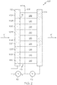
- FIG. 2 another embodiment of the disclosed microplasma night vision device, generally designated 100, may include a photocathode 102, a transparent electrode 104, a plurality of plasma cavities 106 and an accelerating grid 108.
- a first voltage source 110 may apply a first voltage V 1 between the photocathode 102 and the accelerating grid 108 and a second voltage source 112 may apply a second voltage V 2 between the accelerating grid 108 and the transparent electrode 104.
- the photocathode 102, the transparent electrode 104 and the plasma cavities 106 of the microplasma night vision device 100 may be configured as described above in connection with the microplasma night vision device 10.
- the photocathode 102 may be segmented into a plurality of photocathode segments 102A-102I. Each photocathode segment 102A-102I may be associated with a corresponding plasma cavity 106.
- the microplasma night vision device 100 may be constructed and operated in substantially the same way as the microplasma night vision device 10 discussed above. However, as is described in greater detail below, the addition of the accelerating grid 108 may facilitate field emission of electrons from the photocathode 102.
- the accelerating grid 108 may be positioned between the photocathode 102 and the transparent electrode 104, and may be spaced a distance S from the photocathode 102.
- the distance S between the photocathode 102 and the accelerating grid 108 may range from about 0 to about 50 percent of the distance D ( Fig. 1 ) between the photocathode 102 and the transparent electrode, such as from about 5 to about 25 percent of the distance D.
- the first voltage source 110 may apply a first voltage V 1 between the photocathode 102 (negative) and the accelerating grid 108 (positive).
- the first voltage V 1 may establish an electric field. Therefore, when the photocathode 102 is illuminated (arrow A' ), the electric field may induce field emission of electrons from the inner surface 114 of the photocathode 102, and may accelerate the electrons into the plasma cavities 106.
- the second voltage source 112 may apply a second voltage V 2 between the accelerating grid 108 and the transparent electrode 104.
- the second voltage V 2 may be less than, but proximate, the threshold voltage necessary to ionize the ionizable gas and ignite a plasma (e.g., a micro-plasma) within the plasma cavities 106.
- An AC voltage may optionally be used as the second voltage V 2 to inhibit erosion on the transparent electrode 104.
- the field emitted electrons accelerated into the plasma cavities 106 may ignite plasmas within the plasma cavities 106, thereby emitting visible light (arrow B' ) through the transparent electrode 104.
- the magnitude of the first voltage V 1 may be selected such that plasma ignition does not occur in the gap 116 between the photocathode 102 and the accelerating grid 108, but rather only occurs between the accelerating grid 108 and the transparent electrode 104.
- a method for sensing and amplifying incident photons.
- the method 200 may be used in a variety of applications, including but not limited to, night vision (visible and near infrared) and thermal imaging (infrared).
- the method 200 may begin at Block 202 with the step of providing a plurality of plasma cavities.
- the plasma cavities may be arranged in parallel between a photocathode and a transparent electrode.
- Each plasma cavity may house an ionizable gas (or mixture of ionizable gases).
- a voltage may be applied across the plasma cavities.
- the applied voltage may be less (e.g., just less) than the threshold voltage necessary to ionize the ionizable gas and ignite a plasma within the plasma cavities.
- the incident photons may be transduced to electrons.
- the step of transducing the incident photons to electrons may be performed by a photocathode.
- An optional accelerating grid may effect field emission of the electrons from the photocathode.
- the electrons may be introduced to the plasma cavities.
- the electrical energy within the plasma cavities may be sufficient to ignite plasmas within the plasma cavities, thereby outputting visible light (i.e., output photons).
- the disclosed method 200 employs a biasing voltage to generate microplasmas that output photons in response to incident photons, thereby effectively amplifying the incident photons.
- the disclosed microplasma night vision devices and methods generate visible plasmas in response to incident photons and, therefore, function as significantly powerful photon amplifiers.
- the photocathode material e.g., using advanced semiconductor materials
- engineering device topology and plasma ignition parameters it may be possible to achieve photon amplification ratios that are at least about 1 to 2 orders of magnitude higher than may be achieved using current night vision technology, such as Gen III night vision.
Landscapes
- Image-Pickup Tubes, Image-Amplification Tubes, And Storage Tubes (AREA)
- Gas-Filled Discharge Tubes (AREA)
- Transforming Light Signals Into Electric Signals (AREA)
- Photometry And Measurement Of Optical Pulse Characteristics (AREA)
Claims (13)
- Brille mit einer Photonensensorvorrichtung (10), die umfasst:eine Fotokathode (12);eine transparente Elektrode (14), die der Photokathode gegenüberliegt; undmindestens eine Plasmakammer (16), die zwischen der Photokathode und der transparenten Elektrode angeordnet ist, wobei die mindestens eine Plasmakammer ein ionisierbares Gas enthält.
- Brille nach Anspruch 1, ferner mit einer Spannungsquelle (18), wobei die Spannungsquelle eine Spannung über die Plasmakammer anlegt, wobei die Spannung kleiner als eine zum Ionisieren des ionisierbaren Gases erforderliche Schwellenspannung ist.
- Brille nach Anspruch 2, bei der die Spannung mindestens 90 Prozent der Schwellenspannung beträgt.
- Brille nach einem der Ansprüche 1 bis 3, bei der die Photokathode empfindlich auf mindestens eines von sichtbarem Licht und Infrarotlicht reagiert.
- Brille nach einem der Ansprüche 1 bis 4, bei der die Photokathode ein Halbleitermaterial umfasst, wie beispielsweise ein aus der Gruppe bestehend aus Silizium, Galliumarsenid, Indiumgalliumarsenid, Galliumantimonid, Quecksilbercadmiumtellurid, Indiumantimonid und Kombinationen derselben ausgewähltes halbleitendes Material.
- Brille nach einem der Ansprüche 1 bis 5, bei der die transparente Elektrode ein transparentes leitfähiges Oxid umfasst, wie beispielsweise ein aus der Gruppe bestehend aus Indiumzinnoxid, aluminiumdotiertem Zinkoxid, fluordotiertem Zinnoxid und Kombinationen derselben ausgewähltes transparentes leitfähiges Oxid.
- Brille nach einem der Ansprüche 1 bis 6, mit einer Mehrzahl von Plasmakammern, die zwischen der Photokathode und der transparenten Elektrode angeordnet sind, wobei jede Plasmakammer der Mehrzahl von Plasmakammern das ionisierbare Gas enthält.
- Brille nach einem der Ansprüche 1 bis 7, bei der das ionisierbare Gas ein Edelgas umfasst.
- Brille nach einem der Ansprüche 1 bis 8, ferner mit einem Beschleunigungsgitter (108), das zwischen der Photokathode und der transparenten Elektrode angeordnet ist.
- Brille nach Anspruch 9, bei der eine erste Spannungsquelle (110) eine erste Spannung zwischen der Photokathode und dem Beschleunigungsgitter anlegt.
- Brille nach Anspruch 10, bei der eine zweite Spannungsquelle (112) eine zweite Spannung zwischen dem Beschleunigungsgitter und der transparenten Elektrode anlegt.
- Brille nach Anspruch 7 oder einem der Ansprüche 8 bis 11, soweit auf Anspruch 7 rückbezogen, bei der die Mehrzahl der Plasmakammern parallel zwischen der Photokathode und der transparenten Elektrode angeordnet ist.
- Brille nach einem der Ansprüche 1 bis 12, ferner mit einem Objektiv.
Applications Claiming Priority (1)
| Application Number | Priority Date | Filing Date | Title |
|---|---|---|---|
| US13/558,012 US8872094B2 (en) | 2012-07-25 | 2012-07-25 | Microplasma night vision device |
Publications (3)
| Publication Number | Publication Date |
|---|---|
| EP2690644A2 EP2690644A2 (de) | 2014-01-29 |
| EP2690644A3 EP2690644A3 (de) | 2017-08-16 |
| EP2690644B1 true EP2690644B1 (de) | 2019-03-06 |
Family
ID=48877072
Family Applications (1)
| Application Number | Title | Priority Date | Filing Date |
|---|---|---|---|
| EP13177868.0A Not-in-force EP2690644B1 (de) | 2012-07-25 | 2013-07-24 | Mikroplasma-Nachtsichtvorrichtung |
Country Status (4)
| Country | Link |
|---|---|
| US (1) | US8872094B2 (de) |
| EP (1) | EP2690644B1 (de) |
| JP (1) | JP6355900B2 (de) |
| CN (1) | CN103578892B (de) |
Families Citing this family (1)
| Publication number | Priority date | Publication date | Assignee | Title |
|---|---|---|---|---|
| US9960005B2 (en) * | 2012-08-08 | 2018-05-01 | Massachusetts Institute Of Technology | Microplasma generation devices and associated systems and methods |
Citations (2)
| Publication number | Priority date | Publication date | Assignee | Title |
|---|---|---|---|---|
| US5942747A (en) * | 1997-07-28 | 1999-08-24 | Litton Systems, Inc. | Night vision device with voltage to photocathode having a rectified half-sine wave component |
| EP1724623A1 (de) * | 2005-05-18 | 2006-11-22 | Lockheed Martin Corporation | Nachtsichtgerät für fernes Infrarot |
Family Cites Families (8)
| Publication number | Priority date | Publication date | Assignee | Title |
|---|---|---|---|---|
| US3213312A (en) * | 1963-05-22 | 1965-10-19 | Mc Graw Edison Co | Ultraviolet detector tube with a gas filling of hydrogen, helium and a noble gas |
| GB1455011A (en) * | 1973-05-21 | 1976-11-10 | Agfa Gevaert | Electrostatic imaging device and process using same |
| JPS5922351B2 (ja) * | 1976-04-20 | 1984-05-25 | 松下電器産業株式会社 | 発光型スクリ−ン |
| US4039830A (en) * | 1976-08-13 | 1977-08-02 | General Electric Company | Electrostatic x-ray image recording device with mesh-base photocathode photoelectron discriminator means |
| US5311010A (en) * | 1993-02-01 | 1994-05-10 | The United States Of America As Represented By The United States Department Of Energy | Buffer for a gamma-insensitive optical sensor with gas and a buffer assembly |
| US6828730B2 (en) * | 2002-11-27 | 2004-12-07 | Board Of Trustees Of The University Of Illinois | Microdischarge photodetectors |
| CN1854761A (zh) * | 2005-04-29 | 2006-11-01 | 中国科学院西安光学精密机械研究所 | 紫外像增强器 |
| US7804651B2 (en) * | 2008-11-25 | 2010-09-28 | Itt Manufacturing Enterprises, Inc. | Flat field eyepiece |
-
2012
- 2012-07-25 US US13/558,012 patent/US8872094B2/en not_active Expired - Fee Related
-
2013
- 2013-05-22 CN CN201310193963.3A patent/CN103578892B/zh not_active Expired - Fee Related
- 2013-07-24 EP EP13177868.0A patent/EP2690644B1/de not_active Not-in-force
- 2013-07-24 JP JP2013153976A patent/JP6355900B2/ja not_active Expired - Fee Related
Patent Citations (2)
| Publication number | Priority date | Publication date | Assignee | Title |
|---|---|---|---|---|
| US5942747A (en) * | 1997-07-28 | 1999-08-24 | Litton Systems, Inc. | Night vision device with voltage to photocathode having a rectified half-sine wave component |
| EP1724623A1 (de) * | 2005-05-18 | 2006-11-22 | Lockheed Martin Corporation | Nachtsichtgerät für fernes Infrarot |
Also Published As
| Publication number | Publication date |
|---|---|
| EP2690644A3 (de) | 2017-08-16 |
| US8872094B2 (en) | 2014-10-28 |
| CN103578892A (zh) | 2014-02-12 |
| JP2014053292A (ja) | 2014-03-20 |
| CN103578892B (zh) | 2017-10-03 |
| EP2690644A2 (de) | 2014-01-29 |
| JP6355900B2 (ja) | 2018-07-11 |
| US20140027622A1 (en) | 2014-01-30 |
Similar Documents
| Publication | Publication Date | Title |
|---|---|---|
| JP4639379B2 (ja) | バイポーラ型飛行時間質量分析計用のディテクター | |
| EP2880693B1 (de) | Photokathode mit einem siliciumsubstrat mit einer borschicht | |
| WO2016187603A1 (en) | Photocathode including field emitter array on a silicon substrate with boron layer | |
| WO2013045877A1 (en) | Bright source protection for low light imaging sensors | |
| CN207197676U (zh) | 一种日盲紫外单光子成像系统 | |
| Bülter | Single-photon counting detectors for the visible range between 300 and 1,000 nm | |
| Breskin et al. | Recent advances in gaseous imaging photomultipliers | |
| WO2015150765A1 (en) | Ultraviolet light detection | |
| US6836059B2 (en) | Image intensifier and electron multiplier therefor | |
| US8872094B2 (en) | Microplasma night vision device | |
| Barbarino et al. | Proof of feasibility of the vacuum silicon photomultiplier tube (vsipmt) | |
| US12183562B2 (en) | Global shutter for transmission mode secondary electron intensifier by a low voltage signal | |
| CN104505421B (zh) | 一种具有自熄灭自恢复功能的雪崩光电二极管 | |
| US6303918B1 (en) | Method and system for detecting radiation incorporating a hardened photocathode | |
| CN104505422B (zh) | 一种自熄灭自恢复雪崩光电二极管 | |
| Suyama et al. | Development of a multipixel hybrid photodetector with high quantum efficiency and gain | |
| RU141786U1 (ru) | Фотоэлектронный прибор типа проксимити с фотокатодом на основе гетероструктуры а3в5 | |
| Moser | Silicon photomultipliers, a new device for low light level photon detection | |
| CN222029040U (zh) | 一种探测系统及像增强器 | |
| Smith et al. | Development of hybrid photodetectors using single-crystal III–V photocathodes | |
| JP5778179B2 (ja) | 赤外線外部光電子放出検出器 | |
| WO2013007981A1 (en) | Ion detector | |
| Ferenc et al. | First ReFerence photosensor prototype | |
| CN117790264A (zh) | 一种探测系统及像增强器 | |
| CN117954296A (zh) | 一种光电探测装置 |
Legal Events
| Date | Code | Title | Description |
|---|---|---|---|
| PUAI | Public reference made under article 153(3) epc to a published international application that has entered the european phase |
Free format text: ORIGINAL CODE: 0009012 |
|
| AK | Designated contracting states |
Kind code of ref document: A2 Designated state(s): AL AT BE BG CH CY CZ DE DK EE ES FI FR GB GR HR HU IE IS IT LI LT LU LV MC MK MT NL NO PL PT RO RS SE SI SK SM TR |
|
| AX | Request for extension of the european patent |
Extension state: BA ME |
|
| PUAL | Search report despatched |
Free format text: ORIGINAL CODE: 0009013 |
|
| AK | Designated contracting states |
Kind code of ref document: A3 Designated state(s): AL AT BE BG CH CY CZ DE DK EE ES FI FR GB GR HR HU IE IS IT LI LT LU LV MC MK MT NL NO PL PT RO RS SE SI SK SM TR |
|
| AX | Request for extension of the european patent |
Extension state: BA ME |
|
| RIC1 | Information provided on ipc code assigned before grant |
Ipc: H01J 47/02 20060101ALI20170707BHEP Ipc: H01J 31/50 20060101AFI20170707BHEP Ipc: G02B 23/12 20060101ALI20170707BHEP |
|
| STAA | Information on the status of an ep patent application or granted ep patent |
Free format text: STATUS: REQUEST FOR EXAMINATION WAS MADE |
|
| 17P | Request for examination filed |
Effective date: 20180214 |
|
| RBV | Designated contracting states (corrected) |
Designated state(s): AL AT BE BG CH CY CZ DE DK EE ES FI FR GB GR HR HU IE IS IT LI LT LU LV MC MK MT NL NO PL PT RO RS SE SI SK SM TR |
|
| GRAP | Despatch of communication of intention to grant a patent |
Free format text: ORIGINAL CODE: EPIDOSNIGR1 |
|
| STAA | Information on the status of an ep patent application or granted ep patent |
Free format text: STATUS: GRANT OF PATENT IS INTENDED |
|
| INTG | Intention to grant announced |
Effective date: 20180417 |
|
| GRAJ | Information related to disapproval of communication of intention to grant by the applicant or resumption of examination proceedings by the epo deleted |
Free format text: ORIGINAL CODE: EPIDOSDIGR1 |
|
| STAA | Information on the status of an ep patent application or granted ep patent |
Free format text: STATUS: REQUEST FOR EXAMINATION WAS MADE |
|
| GRAP | Despatch of communication of intention to grant a patent |
Free format text: ORIGINAL CODE: EPIDOSNIGR1 |
|
| STAA | Information on the status of an ep patent application or granted ep patent |
Free format text: STATUS: GRANT OF PATENT IS INTENDED |
|
| INTC | Intention to grant announced (deleted) | ||
| INTG | Intention to grant announced |
Effective date: 20180912 |
|
| GRAS | Grant fee paid |
Free format text: ORIGINAL CODE: EPIDOSNIGR3 |
|
| GRAA | (expected) grant |
Free format text: ORIGINAL CODE: 0009210 |
|
| STAA | Information on the status of an ep patent application or granted ep patent |
Free format text: STATUS: THE PATENT HAS BEEN GRANTED |
|
| AK | Designated contracting states |
Kind code of ref document: B1 Designated state(s): AL AT BE BG CH CY CZ DE DK EE ES FI FR GB GR HR HU IE IS IT LI LT LU LV MC MK MT NL NO PL PT RO RS SE SI SK SM TR |
|
| REG | Reference to a national code |
Ref country code: GB Ref legal event code: FG4D |
|
| REG | Reference to a national code |
Ref country code: CH Ref legal event code: EP Ref country code: AT Ref legal event code: REF Ref document number: 1105676 Country of ref document: AT Kind code of ref document: T Effective date: 20190315 |
|
| REG | Reference to a national code |
Ref country code: DE Ref legal event code: R096 Ref document number: 602013051720 Country of ref document: DE |
|
| REG | Reference to a national code |
Ref country code: IE Ref legal event code: FG4D |
|
| REG | Reference to a national code |
Ref country code: NL Ref legal event code: MP Effective date: 20190306 |
|
| REG | Reference to a national code |
Ref country code: LT Ref legal event code: MG4D |
|
| PG25 | Lapsed in a contracting state [announced via postgrant information from national office to epo] |
Ref country code: NO Free format text: LAPSE BECAUSE OF FAILURE TO SUBMIT A TRANSLATION OF THE DESCRIPTION OR TO PAY THE FEE WITHIN THE PRESCRIBED TIME-LIMIT Effective date: 20190606 Ref country code: LT Free format text: LAPSE BECAUSE OF FAILURE TO SUBMIT A TRANSLATION OF THE DESCRIPTION OR TO PAY THE FEE WITHIN THE PRESCRIBED TIME-LIMIT Effective date: 20190306 Ref country code: SE Free format text: LAPSE BECAUSE OF FAILURE TO SUBMIT A TRANSLATION OF THE DESCRIPTION OR TO PAY THE FEE WITHIN THE PRESCRIBED TIME-LIMIT Effective date: 20190306 Ref country code: FI Free format text: LAPSE BECAUSE OF FAILURE TO SUBMIT A TRANSLATION OF THE DESCRIPTION OR TO PAY THE FEE WITHIN THE PRESCRIBED TIME-LIMIT Effective date: 20190306 |
|
| PG25 | Lapsed in a contracting state [announced via postgrant information from national office to epo] |
Ref country code: LV Free format text: LAPSE BECAUSE OF FAILURE TO SUBMIT A TRANSLATION OF THE DESCRIPTION OR TO PAY THE FEE WITHIN THE PRESCRIBED TIME-LIMIT Effective date: 20190306 Ref country code: BG Free format text: LAPSE BECAUSE OF FAILURE TO SUBMIT A TRANSLATION OF THE DESCRIPTION OR TO PAY THE FEE WITHIN THE PRESCRIBED TIME-LIMIT Effective date: 20190606 Ref country code: RS Free format text: LAPSE BECAUSE OF FAILURE TO SUBMIT A TRANSLATION OF THE DESCRIPTION OR TO PAY THE FEE WITHIN THE PRESCRIBED TIME-LIMIT Effective date: 20190306 Ref country code: GR Free format text: LAPSE BECAUSE OF FAILURE TO SUBMIT A TRANSLATION OF THE DESCRIPTION OR TO PAY THE FEE WITHIN THE PRESCRIBED TIME-LIMIT Effective date: 20190607 Ref country code: NL Free format text: LAPSE BECAUSE OF FAILURE TO SUBMIT A TRANSLATION OF THE DESCRIPTION OR TO PAY THE FEE WITHIN THE PRESCRIBED TIME-LIMIT Effective date: 20190306 Ref country code: HR Free format text: LAPSE BECAUSE OF FAILURE TO SUBMIT A TRANSLATION OF THE DESCRIPTION OR TO PAY THE FEE WITHIN THE PRESCRIBED TIME-LIMIT Effective date: 20190306 |
|
| REG | Reference to a national code |
Ref country code: AT Ref legal event code: MK05 Ref document number: 1105676 Country of ref document: AT Kind code of ref document: T Effective date: 20190306 |
|
| PG25 | Lapsed in a contracting state [announced via postgrant information from national office to epo] |
Ref country code: PT Free format text: LAPSE BECAUSE OF FAILURE TO SUBMIT A TRANSLATION OF THE DESCRIPTION OR TO PAY THE FEE WITHIN THE PRESCRIBED TIME-LIMIT Effective date: 20190706 Ref country code: AL Free format text: LAPSE BECAUSE OF FAILURE TO SUBMIT A TRANSLATION OF THE DESCRIPTION OR TO PAY THE FEE WITHIN THE PRESCRIBED TIME-LIMIT Effective date: 20190306 Ref country code: ES Free format text: LAPSE BECAUSE OF FAILURE TO SUBMIT A TRANSLATION OF THE DESCRIPTION OR TO PAY THE FEE WITHIN THE PRESCRIBED TIME-LIMIT Effective date: 20190306 Ref country code: SK Free format text: LAPSE BECAUSE OF FAILURE TO SUBMIT A TRANSLATION OF THE DESCRIPTION OR TO PAY THE FEE WITHIN THE PRESCRIBED TIME-LIMIT Effective date: 20190306 Ref country code: IT Free format text: LAPSE BECAUSE OF FAILURE TO SUBMIT A TRANSLATION OF THE DESCRIPTION OR TO PAY THE FEE WITHIN THE PRESCRIBED TIME-LIMIT Effective date: 20190306 Ref country code: EE Free format text: LAPSE BECAUSE OF FAILURE TO SUBMIT A TRANSLATION OF THE DESCRIPTION OR TO PAY THE FEE WITHIN THE PRESCRIBED TIME-LIMIT Effective date: 20190306 Ref country code: CZ Free format text: LAPSE BECAUSE OF FAILURE TO SUBMIT A TRANSLATION OF THE DESCRIPTION OR TO PAY THE FEE WITHIN THE PRESCRIBED TIME-LIMIT Effective date: 20190306 Ref country code: RO Free format text: LAPSE BECAUSE OF FAILURE TO SUBMIT A TRANSLATION OF THE DESCRIPTION OR TO PAY THE FEE WITHIN THE PRESCRIBED TIME-LIMIT Effective date: 20190306 |
|
| PG25 | Lapsed in a contracting state [announced via postgrant information from national office to epo] |
Ref country code: PL Free format text: LAPSE BECAUSE OF FAILURE TO SUBMIT A TRANSLATION OF THE DESCRIPTION OR TO PAY THE FEE WITHIN THE PRESCRIBED TIME-LIMIT Effective date: 20190306 Ref country code: SM Free format text: LAPSE BECAUSE OF FAILURE TO SUBMIT A TRANSLATION OF THE DESCRIPTION OR TO PAY THE FEE WITHIN THE PRESCRIBED TIME-LIMIT Effective date: 20190306 |
|
| REG | Reference to a national code |
Ref country code: DE Ref legal event code: R097 Ref document number: 602013051720 Country of ref document: DE |
|
| PG25 | Lapsed in a contracting state [announced via postgrant information from national office to epo] |
Ref country code: IS Free format text: LAPSE BECAUSE OF FAILURE TO SUBMIT A TRANSLATION OF THE DESCRIPTION OR TO PAY THE FEE WITHIN THE PRESCRIBED TIME-LIMIT Effective date: 20190706 Ref country code: AT Free format text: LAPSE BECAUSE OF FAILURE TO SUBMIT A TRANSLATION OF THE DESCRIPTION OR TO PAY THE FEE WITHIN THE PRESCRIBED TIME-LIMIT Effective date: 20190306 |
|
| PLBE | No opposition filed within time limit |
Free format text: ORIGINAL CODE: 0009261 |
|
| STAA | Information on the status of an ep patent application or granted ep patent |
Free format text: STATUS: NO OPPOSITION FILED WITHIN TIME LIMIT |
|
| REG | Reference to a national code |
Ref country code: DE Ref legal event code: R082 Ref document number: 602013051720 Country of ref document: DE Representative=s name: MAIER, LL.M., MICHAEL C., DE Ref country code: DE Ref legal event code: R082 Ref document number: 602013051720 Country of ref document: DE Representative=s name: BOULT WADE TENNANT LLP, DE |
|
| PG25 | Lapsed in a contracting state [announced via postgrant information from national office to epo] |
Ref country code: DK Free format text: LAPSE BECAUSE OF FAILURE TO SUBMIT A TRANSLATION OF THE DESCRIPTION OR TO PAY THE FEE WITHIN THE PRESCRIBED TIME-LIMIT Effective date: 20190306 |
|
| 26N | No opposition filed |
Effective date: 20191209 |
|
| REG | Reference to a national code |
Ref country code: DE Ref legal event code: R082 Ref document number: 602013051720 Country of ref document: DE Representative=s name: BOULT WADE TENNANT LLP, DE |
|
| PG25 | Lapsed in a contracting state [announced via postgrant information from national office to epo] |
Ref country code: MC Free format text: LAPSE BECAUSE OF FAILURE TO SUBMIT A TRANSLATION OF THE DESCRIPTION OR TO PAY THE FEE WITHIN THE PRESCRIBED TIME-LIMIT Effective date: 20190306 Ref country code: SI Free format text: LAPSE BECAUSE OF FAILURE TO SUBMIT A TRANSLATION OF THE DESCRIPTION OR TO PAY THE FEE WITHIN THE PRESCRIBED TIME-LIMIT Effective date: 20190306 |
|
| REG | Reference to a national code |
Ref country code: CH Ref legal event code: PL |
|
| PG25 | Lapsed in a contracting state [announced via postgrant information from national office to epo] |
Ref country code: TR Free format text: LAPSE BECAUSE OF FAILURE TO SUBMIT A TRANSLATION OF THE DESCRIPTION OR TO PAY THE FEE WITHIN THE PRESCRIBED TIME-LIMIT Effective date: 20190306 |
|
| REG | Reference to a national code |
Ref country code: BE Ref legal event code: MM Effective date: 20190731 |
|
| PG25 | Lapsed in a contracting state [announced via postgrant information from national office to epo] |
Ref country code: BE Free format text: LAPSE BECAUSE OF NON-PAYMENT OF DUE FEES Effective date: 20190731 Ref country code: LU Free format text: LAPSE BECAUSE OF NON-PAYMENT OF DUE FEES Effective date: 20190724 Ref country code: LI Free format text: LAPSE BECAUSE OF NON-PAYMENT OF DUE FEES Effective date: 20190731 Ref country code: CH Free format text: LAPSE BECAUSE OF NON-PAYMENT OF DUE FEES Effective date: 20190731 |
|
| PG25 | Lapsed in a contracting state [announced via postgrant information from national office to epo] |
Ref country code: IE Free format text: LAPSE BECAUSE OF NON-PAYMENT OF DUE FEES Effective date: 20190724 |
|
| PG25 | Lapsed in a contracting state [announced via postgrant information from national office to epo] |
Ref country code: CY Free format text: LAPSE BECAUSE OF FAILURE TO SUBMIT A TRANSLATION OF THE DESCRIPTION OR TO PAY THE FEE WITHIN THE PRESCRIBED TIME-LIMIT Effective date: 20190306 |
|
| PG25 | Lapsed in a contracting state [announced via postgrant information from national office to epo] |
Ref country code: HU Free format text: LAPSE BECAUSE OF FAILURE TO SUBMIT A TRANSLATION OF THE DESCRIPTION OR TO PAY THE FEE WITHIN THE PRESCRIBED TIME-LIMIT; INVALID AB INITIO Effective date: 20130724 Ref country code: MT Free format text: LAPSE BECAUSE OF FAILURE TO SUBMIT A TRANSLATION OF THE DESCRIPTION OR TO PAY THE FEE WITHIN THE PRESCRIBED TIME-LIMIT Effective date: 20190306 |
|
| PGFP | Annual fee paid to national office [announced via postgrant information from national office to epo] |
Ref country code: FR Payment date: 20210726 Year of fee payment: 9 |
|
| PGFP | Annual fee paid to national office [announced via postgrant information from national office to epo] |
Ref country code: DE Payment date: 20210728 Year of fee payment: 9 Ref country code: GB Payment date: 20210727 Year of fee payment: 9 |
|
| PG25 | Lapsed in a contracting state [announced via postgrant information from national office to epo] |
Ref country code: MK Free format text: LAPSE BECAUSE OF FAILURE TO SUBMIT A TRANSLATION OF THE DESCRIPTION OR TO PAY THE FEE WITHIN THE PRESCRIBED TIME-LIMIT Effective date: 20190306 |
|
| REG | Reference to a national code |
Ref country code: DE Ref legal event code: R119 Ref document number: 602013051720 Country of ref document: DE |
|
| GBPC | Gb: european patent ceased through non-payment of renewal fee |
Effective date: 20220724 |
|
| PG25 | Lapsed in a contracting state [announced via postgrant information from national office to epo] |
Ref country code: FR Free format text: LAPSE BECAUSE OF NON-PAYMENT OF DUE FEES Effective date: 20220731 |
|
| PG25 | Lapsed in a contracting state [announced via postgrant information from national office to epo] |
Ref country code: GB Free format text: LAPSE BECAUSE OF NON-PAYMENT OF DUE FEES Effective date: 20220724 Ref country code: DE Free format text: LAPSE BECAUSE OF NON-PAYMENT OF DUE FEES Effective date: 20230201 |