EP2685488A1 - Production method for semiconductor device - Google Patents
Production method for semiconductor device Download PDFInfo
- Publication number
- EP2685488A1 EP2685488A1 EP11860559.1A EP11860559A EP2685488A1 EP 2685488 A1 EP2685488 A1 EP 2685488A1 EP 11860559 A EP11860559 A EP 11860559A EP 2685488 A1 EP2685488 A1 EP 2685488A1
- Authority
- EP
- European Patent Office
- Prior art keywords
- substrate
- semiconductor device
- protective film
- manufacturing
- silicon carbide
- Prior art date
- Legal status (The legal status is an assumption and is not a legal conclusion. Google has not performed a legal analysis and makes no representation as to the accuracy of the status listed.)
- Withdrawn
Links
Images



Classifications
-
- H—ELECTRICITY
- H10—SEMICONDUCTOR DEVICES; ELECTRIC SOLID-STATE DEVICES NOT OTHERWISE PROVIDED FOR
- H10P—GENERIC PROCESSES OR APPARATUS FOR THE MANUFACTURE OR TREATMENT OF DEVICES COVERED BY CLASS H10
- H10P95/00—Generic processes or apparatus for manufacture or treatments not covered by the other groups of this subclass
- H10P95/90—Thermal treatments, e.g. annealing or sintering
- H10P95/906—Thermal treatments, e.g. annealing or sintering for altering the shape of semiconductors, e.g. smoothing the surface
-
- H—ELECTRICITY
- H10—SEMICONDUCTOR DEVICES; ELECTRIC SOLID-STATE DEVICES NOT OTHERWISE PROVIDED FOR
- H10D—INORGANIC ELECTRIC SEMICONDUCTOR DEVICES
- H10D12/00—Bipolar devices controlled by the field effect, e.g. insulated-gate bipolar transistors [IGBT]
- H10D12/01—Manufacture or treatment
- H10D12/031—Manufacture or treatment of IGBTs
-
- H—ELECTRICITY
- H10—SEMICONDUCTOR DEVICES; ELECTRIC SOLID-STATE DEVICES NOT OTHERWISE PROVIDED FOR
- H10D—INORGANIC ELECTRIC SEMICONDUCTOR DEVICES
- H10D30/00—Field-effect transistors [FET]
- H10D30/01—Manufacture or treatment
- H10D30/021—Manufacture or treatment of FETs having insulated gates [IGFET]
- H10D30/028—Manufacture or treatment of FETs having insulated gates [IGFET] of double-diffused metal oxide semiconductor [DMOS] FETs
- H10D30/0291—Manufacture or treatment of FETs having insulated gates [IGFET] of double-diffused metal oxide semiconductor [DMOS] FETs of vertical DMOS [VDMOS] FETs
-
- H—ELECTRICITY
- H10—SEMICONDUCTOR DEVICES; ELECTRIC SOLID-STATE DEVICES NOT OTHERWISE PROVIDED FOR
- H10D—INORGANIC ELECTRIC SEMICONDUCTOR DEVICES
- H10D30/00—Field-effect transistors [FET]
- H10D30/60—Insulated-gate field-effect transistors [IGFET]
- H10D30/64—Double-diffused metal-oxide semiconductor [DMOS] FETs
- H10D30/66—Vertical DMOS [VDMOS] FETs
-
- H—ELECTRICITY
- H10—SEMICONDUCTOR DEVICES; ELECTRIC SOLID-STATE DEVICES NOT OTHERWISE PROVIDED FOR
- H10D—INORGANIC ELECTRIC SEMICONDUCTOR DEVICES
- H10D62/00—Semiconductor bodies, or regions thereof, of devices having potential barriers
- H10D62/80—Semiconductor bodies, or regions thereof, of devices having potential barriers characterised by the materials
- H10D62/83—Semiconductor bodies, or regions thereof, of devices having potential barriers characterised by the materials being Group IV materials, e.g. B-doped Si or undoped Ge
- H10D62/832—Semiconductor bodies, or regions thereof, of devices having potential barriers characterised by the materials being Group IV materials, e.g. B-doped Si or undoped Ge being Group IV materials comprising two or more elements, e.g. SiGe
- H10D62/8325—Silicon carbide
-
- H—ELECTRICITY
- H10—SEMICONDUCTOR DEVICES; ELECTRIC SOLID-STATE DEVICES NOT OTHERWISE PROVIDED FOR
- H10P—GENERIC PROCESSES OR APPARATUS FOR THE MANUFACTURE OR TREATMENT OF DEVICES COVERED BY CLASS H10
- H10P14/00—Formation of materials, e.g. in the shape of layers or pillars
- H10P14/20—Formation of materials, e.g. in the shape of layers or pillars of semiconductor materials
-
- H—ELECTRICITY
- H10—SEMICONDUCTOR DEVICES; ELECTRIC SOLID-STATE DEVICES NOT OTHERWISE PROVIDED FOR
- H10P—GENERIC PROCESSES OR APPARATUS FOR THE MANUFACTURE OR TREATMENT OF DEVICES COVERED BY CLASS H10
- H10P14/00—Formation of materials, e.g. in the shape of layers or pillars
- H10P14/60—Formation of materials, e.g. in the shape of layers or pillars of insulating materials
- H10P14/63—Formation of materials, e.g. in the shape of layers or pillars of insulating materials characterised by the formation processes
- H10P14/6326—Deposition processes
- H10P14/6349—Deposition of epitaxial materials
-
- H—ELECTRICITY
- H10—SEMICONDUCTOR DEVICES; ELECTRIC SOLID-STATE DEVICES NOT OTHERWISE PROVIDED FOR
- H10P—GENERIC PROCESSES OR APPARATUS FOR THE MANUFACTURE OR TREATMENT OF DEVICES COVERED BY CLASS H10
- H10P30/00—Ion implantation into wafers, substrates or parts of devices
- H10P30/20—Ion implantation into wafers, substrates or parts of devices into semiconductor materials, e.g. for doping
- H10P30/202—Ion implantation into wafers, substrates or parts of devices into semiconductor materials, e.g. for doping characterised by the semiconductor materials
- H10P30/204—Ion implantation into wafers, substrates or parts of devices into semiconductor materials, e.g. for doping characterised by the semiconductor materials into Group IV semiconductors
- H10P30/2042—Ion implantation into wafers, substrates or parts of devices into semiconductor materials, e.g. for doping characterised by the semiconductor materials into Group IV semiconductors into crystalline silicon carbide
-
- H—ELECTRICITY
- H10—SEMICONDUCTOR DEVICES; ELECTRIC SOLID-STATE DEVICES NOT OTHERWISE PROVIDED FOR
- H10P—GENERIC PROCESSES OR APPARATUS FOR THE MANUFACTURE OR TREATMENT OF DEVICES COVERED BY CLASS H10
- H10P30/00—Ion implantation into wafers, substrates or parts of devices
- H10P30/20—Ion implantation into wafers, substrates or parts of devices into semiconductor materials, e.g. for doping
- H10P30/21—Ion implantation into wafers, substrates or parts of devices into semiconductor materials, e.g. for doping of electrically active species
-
- H—ELECTRICITY
- H10—SEMICONDUCTOR DEVICES; ELECTRIC SOLID-STATE DEVICES NOT OTHERWISE PROVIDED FOR
- H10P—GENERIC PROCESSES OR APPARATUS FOR THE MANUFACTURE OR TREATMENT OF DEVICES COVERED BY CLASS H10
- H10P30/00—Ion implantation into wafers, substrates or parts of devices
- H10P30/20—Ion implantation into wafers, substrates or parts of devices into semiconductor materials, e.g. for doping
- H10P30/28—Ion implantation into wafers, substrates or parts of devices into semiconductor materials, e.g. for doping characterised by an annealing step, e.g. for activation of dopants
-
- H—ELECTRICITY
- H10—SEMICONDUCTOR DEVICES; ELECTRIC SOLID-STATE DEVICES NOT OTHERWISE PROVIDED FOR
- H10P—GENERIC PROCESSES OR APPARATUS FOR THE MANUFACTURE OR TREATMENT OF DEVICES COVERED BY CLASS H10
- H10P95/00—Generic processes or apparatus for manufacture or treatments not covered by the other groups of this subclass
- H10P95/90—Thermal treatments, e.g. annealing or sintering
-
- H—ELECTRICITY
- H10—SEMICONDUCTOR DEVICES; ELECTRIC SOLID-STATE DEVICES NOT OTHERWISE PROVIDED FOR
- H10D—INORGANIC ELECTRIC SEMICONDUCTOR DEVICES
- H10D12/00—Bipolar devices controlled by the field effect, e.g. insulated-gate bipolar transistors [IGBT]
- H10D12/01—Manufacture or treatment
- H10D12/031—Manufacture or treatment of IGBTs
- H10D12/032—Manufacture or treatment of IGBTs of vertical IGBTs
Definitions
- the present invention relates to a method of manufacturing a semiconductor device, and more particularly to a method of manufacturing a semiconductor device capable of suppressing surface roughness of a substrate made of silicon carbide during activation annealing for activating an impurity introduced into the substrate.
- silicon carbide has been increasingly used as a material for a semiconductor device in order to realize a higher breakdown voltage, loss reduction, use in a high-temperature environment and the like of the semiconductor device.
- Silicon carbide is a wide band gap semiconductor having a wider band gap than that of silicon which has been conventionally and widely used as a material for a semiconductor device.
- a semiconductor device made of silicon carbide also has the advantage of exhibiting less performance degradation when used in a high-temperature environment than a semiconductor device made of silicon.
- a desired impurity is introduced into a substrate made of silicon carbide, and then activation annealing for activating the impurity is carried out.
- the activation annealing of the substrate made of silicon carbide needs to be carried out at a high temperature.
- surface roughness of the substrate may occur due to the activation annealing. It is desirable to reduce this surface roughness since it may adversely affect the performance of the manufactured semiconductor device.
- Patent Literature 1 Japanese Patent Laying-Open No. 7-86199
- the substrate needs to be heated to a high temperature of 1600°C or more.
- a crack may occur in the silicon nitride film due to the difference in coefficient of linear expansion between silicon carbide and silicon nitride and the like. If a crack occurs in the silicon nitride film serving as a protective film, surface roughness of the substrate cannot be sufficiently suppressed.
- the present invention was made to address such problems, and an object of the present invention is to provide a method of manufacturing a semiconductor device capable of suppressing surface roughness during activation annealing of a substrate made of silicon carbide.
- a method of manufacturing a semiconductor device includes the steps of preparing a substrate made of silicon carbide, performing ion implantation into the substrate, forming a protective film made of silicon dioxide on the substrate into which the ion implantation was performed, and heating the substrate on which the protective film was formed to a temperature range of 1600°C or more in an atmosphere containing gas including an oxygen atom.
- the protective film made of silicon dioxide is formed on the substrate made of silicon carbide into which the ion implantation was performed, and then activation annealing is carried out by heating the substrate to the temperature range of 1600°C or more in the atmosphere containing the gas including an oxygen atom.
- activation annealing is carried out by heating the substrate to the temperature range of 1600°C or more in the atmosphere containing the gas including an oxygen atom.
- the substrate on which the protective film was formed may be heated to a temperature range of 1700°C or less.
- the heating temperature of the substrate By setting the heating temperature of the substrate to 1700°C or less, surface roughness of the substrate can be more reliably suppressed by the protective film made of silicon dioxide.
- the substrate on which the protective film was formed is heated in an atmosphere containing oxygen gas.
- Oxygen gas is inexpensive and easy to handle, and is thus suitable as the gas constituting the atmosphere (the gas including an oxygen atom) in the above step of heating the substrate.
- the protective film in the step of forming a protective film, may be formed by thermal oxidation.
- the protective film made of silicon dioxide can be readily formed.
- the step of forming a protective film and the step of heating the substrate may be performed as a single step.
- the substrate is heated in the atmosphere containing the gas including an oxygen atom.
- the step of forming a protective film and the subsequent step of heating the substrate in the atmosphere containing the gas including an oxygen atom can be performed as a single step. Accordingly, the manufacturing process of the semiconductor device can be simplified.
- a method of manufacturing a semiconductor device capable of suppressing surface roughness during activation annealing of a substrate made of silicon carbide can be provided.
- a MOSFET 100 which is a semiconductor device is a DiMOSFET, and includes a silicon carbide substrate 1 of an n conductivity type (first conductivity type), a buffer layer 2 of the n conductivity type made of silicon carbide, a drift layer 3 of the n conductivity type made of silicon carbide, a pair of p type body regions 4 of a p conductivity type (second conductivity type), n + regions 5 of the n conductivity type, and p + regions 6 of the p conductivity type.
- Buffer layer 2 is formed on one main surface 1A of silicon carbide substrate 1, and is of the n conductivity type by containing an n type impurity.
- Drift layer 3 is formed on buffer layer 2, and is of the n conductivity type by containing an n type impurity.
- the n type impurity contained in drift layer 3 is N (nitrogen), for example, and is contained in a concentration (density) lower than that of the n type impurity contained in buffer layer 2.
- Buffer layer 2 and drift layer 3 constitute an epitaxial growth layer formed on one main surface 1A of silicon carbide substrate 1.
- the pair of p type body regions 4 is formed apart from each other in the epitaxial growth layer to include a main surface 3A opposite to a main surface closer to silicon carbide substrate 1, and is of the p conductivity type by containing a p type impurity (an impurity of the p conductivity type).
- the p type impurity contained in p type body regions 4 is aluminum (Al) and/or boron (B), for example.
- Each of n + regions 5 is formed in each of the pair of p type body regions 4 to include main surface 3A and be surrounded by each of p type body regions 4.
- N + regions 5 contain an n type impurity such as P in a concentration (density) higher than that of the n type impurity contained in drift layer 3.
- Each of p + regions 6 is formed in each of the pair of p type body regions 4 to include main surface 3A, be surrounded by each of p type body regions 4, and be adjacent to each of n + regions 5.
- P + regions 6 contain a p type impurity such as Al in a concentration (density) higher than that of the p type impurity contained in p type body regions 4.
- Buffer layer 2, drift layer 3, p type body regions 4, n + regions 5 and p + regions 6 constitute an active layer 7.
- MOSFET 100 further includes a gate oxide film 91 as a gate insulating film, a gate electrode 93, a pair of source contact electrodes 92, an interlayer insulating film 94, a source line 95, and a drain electrode 96.
- Gate oxide film 91 is formed on and in contact with main surface 3A of the epitaxial growth layer to extend from an upper surface of one of n + regions 5 to an upper surface of the other n + region 5, and is made of silicon dioxide (SiO 2 ), for example.
- Gate electrode 93 is arranged in contact with gate oxide film 91 to extend from above one of n + regions 5 to above the other n + region 5.
- Gate electrode 93 is formed of a conductor such as polysilicon including an impurity or Al.
- Source contact electrodes 92 is arranged in contact with main surface 3A to extend from a top portion of each of the pair of n + regions 5 in a direction away from gate oxide film 91 to reach a top portion of each of p + regions 6.
- Source contact electrodes 92 are made of a material capable of making ohmic contact with n + regions 5, such as Ni x Si y (nickel silicide).
- Interlayer insulating film 94 is formed to surround gate electrode 93 above main surface 3A of drift layer 3 and extend from above one of p type body regions 4 to above the other p type body region 4, and is made of silicon dioxide (SiO 2 ) which is an insulator, for example.
- Source line 95 surrounds interlayer insulating film 94 above main surface 3A of drift layer 3, and extends to upper surfaces of source contact electrodes 92.
- Source line 95 is formed of a conductor such as Al, and is electrically connected to n + regions 5 via source contact electrodes 92.
- Drain electrode 96 is formed in contact with a main surface of silicon carbide substrate 1 opposite to the surface on which drift layer 3 is formed.
- This drain electrode 96 is made of a material capable of making ohmic contact with silicon carbide substrate 1, such as Ni x Si y , and is electrically connected to silicon carbide substrate 1.
- MOSFET 100 when gate electrode 93 has a voltage lower than a threshold voltage, i.e., in an off state, a pn junction between each of p type body regions 4 and drift layer 3 located immediately below gate oxide film 91 is reverse biased and non-conducting even if a voltage is applied to the drain electrode.
- a voltage equal to or higher than the threshold voltage is applied to gate electrode 93, an inversion layer is formed in a channel region in p type body region 4 which is in contact with gate oxide film 91.
- n + regions 5 and drift layer 3 are electrically connected to each other, causing a current to flow between source line 95 and drain electrode 96.
- the inversion layer is formed in the channel region in p type body region 4 which is in contact with gate oxide film 91, and a current flows through the inversion layer. If surface roughness occurs in main surface 3A, therefore, resistance in the inversion layer (channel resistance) increases to increase on-resistance. Nevertheless, surface roughness of main surface 3A is reduced and the occurrence of the above problem is suppressed in MOSFET 100 in this embodiment, which is manufactured with the method of manufacturing a semiconductor device in this embodiment to be described below.
- a silicon carbide substrate preparation step is first performed as a step (S110).
- silicon carbide substrate 1 obtained by slicing an ingot that has been manufactured with a sublimation method, for example, is prepared.
- an epitaxial growth step is performed as a step (S 120).
- step (S120) referring to Fig. 3 , buffer layer 2 and drift layer 3 made of silicon carbide are successively formed by epitaxial growth on one main surface 1A of silicon carbide substrate 1.
- a substrate 8 with an epitaxial growth layer is obtained as a substrate made of silicon carbide.
- an ion implantation step is performed as a step (S 130).
- ion implantation for forming p type body regions 4 is first performed. Specifically, Al (aluminum) ions are implanted into drift layer 3, for example, to form p type body regions 4. Then, ion implantation for forming n + regions 5 is performed. Specifically, P (phosphor) ions are implanted into p type body regions 4, for example, to form n + regions 5 in p type body regions 4. Further, ion implantation for forming p + regions 6 is performed.
- Al ions are implanted into p type body regions 4, for example, to form p + regions 6 in p type body regions 4.
- a mask layer which is made of silicon dioxide (SiO 2 ) and has an opening in a desired region where the ion implantation is to be performed, on a main surface of drift layer 3.
- a protective film formation step is performed as a step (S 140).
- a protective film 80 made of silicon dioxide is formed on main surface 3A of substrate 8 with the epitaxial growth layer into which the ion implantation was performed in step (S 130).
- This protective film 80 can be formed by thermal oxidation, for example.
- Protective film 80 can have a thickness of 0.1 ⁇ m or more and 1 ⁇ m or less, for example.
- Protective film 80 may be formed by CVD (Chemical Vapor Deposition) such as plasma CVD.
- step (S150) an activation annealing step is performed as a step (S150).
- substrate 8 with the epitaxial growth layer on which protective film 80 was formed in step (S 140) is heated to a temperature range of 1600°C or more in an atmosphere containing gas including an oxygen atom.
- the impurities introduced into substrate 8 with the epitaxial growth layer by the ion implantation in step (S 130) are activated, and p type body regions 4, n + regions 5 and p + regions 6 of the desired conductivity types are obtained.
- step (S150) if substrate 8 with the epitaxial growth layer is heated in an argon gas atmosphere in step (S150), for example, cracks 80A may occur in protective film 80 due to the difference in coefficient of linear expansion between silicon carbide and silicon dioxide and the like, as shown in Fig. 6 .
- a silicon atom that has left substrate 8 with the epitaxial growth layer is released into the atmosphere through cracks 80A. As a result, surface roughness occurs.
- step (S 150) in this embodiment substrate 8 with the epitaxial growth layer is heated in the atmosphere containing the gas including an oxygen atom. Accordingly, silicon that has left substrate 8 with the epitaxial growth layer is bonded to oxygen in the atmosphere, and becomes silicon dioxide. As a result, as shown in Fig. 7 , a silicon dioxide film 82 is formed in a boundary portion between substrate 8 with the epitaxial growth layer and protective film 80, and crack suppression portions 81 made of silicon dioxide and filling (repairing) cracks 80A are formed. The occurrence and growth of cracks 80A is thus suppressed, thereby reducing the occurrence of surface roughness.
- oxygen gas for example, oxygen gas, ozone gas, nitrogen monoxide gas, nitrogen dioxide gas, or carbon monoxide gas may be employed as the above gas including an oxygen atom.
- Oxygen gas is inexpensive and easy to handle, and is thus particularly suitable as the above gas including an oxygen atom.
- substrate 8 with the epitaxial growth layer may be heated in an oxygen gas atmosphere, or in an atmosphere containing oxygen gas and argon gas and including an impurity as the remainder.
- step (S 150) it is preferable that the heating temperature of substrate 8 with the epitaxial growth layer be set to 1700°C or less.
- the heating temperature of substrate 8 with the epitaxial growth layer be set to 1700°C or less.
- steps (S 140) and (S150) may be performed as a single step.
- protective film 80 is formed by heating substrate 8 with the epitaxial growth layer to a temperature range of 1100°C or more and 1600°C or less in a reaction chamber adjusted to an atmosphere containing oxygen gas and argon gas and including an impurity as the remainder and maintaining the substrate for a period of 5 minutes or more and 120 minutes or less, and then activation annealing is carried out by heating the substrate to a temperature range of 1600°C or more and 1700°C or less in the same reaction chamber without changing the atmosphere and maintaining the substrate for a period of 1 minute or more and 30 minutes or less.
- a protective film removal step is performed as a step (S 160).
- protective film 80 is removed.
- Protective film 80 may be removed with liquid containing hydrofluoric acid, or in a plasma process using fluorine, for example.
- oxide film (gate oxide film) 91 is formed by conducting heat treatment of heating the substrate to 1300°C in an oxygen atmosphere and maintaining the substrate for 60 minutes, for example.
- an electrode formation step is performed as a step (S 180).
- gate electrode 93 made of polysilicon which is a conductor including a high concentration of impurity is formed by CVD, photolithography and etching, for example.
- interlayer insulating film 94 made of SiO 2 which is an insulator is formed by CVD, for example, to surround gate electrode 93 above main surface 3A.
- interlayer insulating film 94 and oxide film 91 in a region where source contact electrode 92 is to be formed are removed by photolithography and etching.
- a nickel (Ni) film formed by an evaporation method for example, is heated and silicidized, to form source contact electrode 92 and drain electrode 96.
- source line 95 made of Al which is a conductor is formed by an evaporation method, for example, to surround interlayer insulating film 94 above main surface 3A and extend to the upper surfaces of n + regions 5 and source contact electrodes 92.
- MOSFET 100 in this embodiment is completed.
- the method of manufacturing a semiconductor device of the present invention is widely applicable to methods of manufacturing semiconductor devices employing a process of performing ion implantation into a substrate made of silicon carbide, and then carrying out activation annealing, and is more specifically applicable to methods of manufacturing a JFET (Junction Field Effect Transistor), an IGBT (Insulated Gate Bipolar Transistor) and the like.
- JFET Joint Field Effect Transistor
- IGBT Insulated Gate Bipolar Transistor
- the method of manufacturing a semiconductor device of the present invention is particularly advantageously applicable to a method of manufacturing a semiconductor device employing a process of performing ion implantation into a substrate made of silicon carbide, and then carrying out activation annealing.
Landscapes
- Electrodes Of Semiconductors (AREA)
- Recrystallisation Techniques (AREA)
Abstract
Description
- The present invention relates to a method of manufacturing a semiconductor device, and more particularly to a method of manufacturing a semiconductor device capable of suppressing surface roughness of a substrate made of silicon carbide during activation annealing for activating an impurity introduced into the substrate.
- In recent years, silicon carbide has been increasingly used as a material for a semiconductor device in order to realize a higher breakdown voltage, loss reduction, use in a high-temperature environment and the like of the semiconductor device. Silicon carbide is a wide band gap semiconductor having a wider band gap than that of silicon which has been conventionally and widely used as a material for a semiconductor device. By using silicon carbide as a material for a semiconductor device, therefore, a higher breakdown voltage, on-resistance reduction and the like of the semiconductor device can be achieved. A semiconductor device made of silicon carbide also has the advantage of exhibiting less performance degradation when used in a high-temperature environment than a semiconductor device made of silicon.
- In a method of manufacturing such semiconductor device made of silicon carbide, a desired impurity is introduced into a substrate made of silicon carbide, and then activation annealing for activating the impurity is carried out. Here, the activation annealing of the substrate made of silicon carbide needs to be carried out at a high temperature. As a result, surface roughness of the substrate may occur due to the activation annealing. It is desirable to reduce this surface roughness since it may adversely affect the performance of the manufactured semiconductor device.
- To address this problem, a method of manufacturing a silicon carbide semiconductor device has been proposed, in which a surface of a region into which ion implantation was performed is covered with a silicon nitride film prior to activation annealing of an impurity introduced by the ion implantation (e.g., see Japanese Patent Laying-Open No.
7-86199 - PTL 1: Japanese Patent Laying-Open No.
7-86199 - During the above activation annealing, however, the substrate needs to be heated to a high temperature of 1600°C or more. In the method of manufacturing a semiconductor device described in
Patent Literature 1, therefore, a crack may occur in the silicon nitride film due to the difference in coefficient of linear expansion between silicon carbide and silicon nitride and the like. If a crack occurs in the silicon nitride film serving as a protective film, surface roughness of the substrate cannot be sufficiently suppressed. - The present invention was made to address such problems, and an object of the present invention is to provide a method of manufacturing a semiconductor device capable of suppressing surface roughness during activation annealing of a substrate made of silicon carbide.
- A method of manufacturing a semiconductor device according to the present invention includes the steps of preparing a substrate made of silicon carbide, performing ion implantation into the substrate, forming a protective film made of silicon dioxide on the substrate into which the ion implantation was performed, and heating the substrate on which the protective film was formed to a temperature range of 1600°C or more in an atmosphere containing gas including an oxygen atom.
- In the method of manufacturing a semiconductor device of the present invention, the protective film made of silicon dioxide is formed on the substrate made of silicon carbide into which the ion implantation was performed, and then activation annealing is carried out by heating the substrate to the temperature range of 1600°C or more in the atmosphere containing the gas including an oxygen atom. Here, even if a crack may occur in the protective film made of silicon dioxide, the occurrence of the crack is suppressed by silicon dioxide produced by bonding between silicon that leaves the silicon carbide substrate and an oxygen atom contained in the gas in the atmosphere. As a result, according to the method of manufacturing a semiconductor device of the present invention, surface roughness during the activation annealing of the substrate made of silicon carbide can be suppressed.
- In the above method of manufacturing a semiconductor device of the present invention, in the step of heating the substrate, the substrate on which the protective film was formed may be heated to a temperature range of 1700°C or less. By setting the heating temperature of the substrate to 1700°C or less, surface roughness of the substrate can be more reliably suppressed by the protective film made of silicon dioxide.
- In the above method of manufacturing a semiconductor device of the present invention, in the step of heating the substrate, the substrate on which the protective film was formed is heated in an atmosphere containing oxygen gas.
- Oxygen gas is inexpensive and easy to handle, and is thus suitable as the gas constituting the atmosphere (the gas including an oxygen atom) in the above step of heating the substrate.
- In the above method of manufacturing a semiconductor device of the present invention, in the step of forming a protective film, the protective film may be formed by thermal oxidation. In this case, the protective film made of silicon dioxide can be readily formed.
- In the above method of manufacturing a semiconductor device of the present invention, the step of forming a protective film and the step of heating the substrate may be performed as a single step.
- If the protective film is formed in a thermal oxidation process, the substrate is heated in the atmosphere containing the gas including an oxygen atom. Thus, the step of forming a protective film and the subsequent step of heating the substrate in the atmosphere containing the gas including an oxygen atom can be performed as a single step. Accordingly, the manufacturing process of the semiconductor device can be simplified.
- As is clear from the above description, according to the method of manufacturing a semiconductor device of the present invention, a method of manufacturing a semiconductor device capable of suppressing surface roughness during activation annealing of a substrate made of silicon carbide can be provided.
-
-
Fig. 1 is a schematic cross-sectional view showing a structure of a MOSFET (Metal Oxide Semiconductor Field Effect Transistor) in one embodiment of the present invention. -
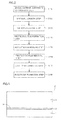
Fig. 2 is a flowchart schematically illustrating a method of manufacturing the MOSFET. -
Fig. 3 is a schematic cross-sectional view for explaining the method of manufacturing the MOSFET. -
Fig. 4 is a schematic cross-sectional view for explaining the method of manufacturing the MOSFET. -
Fig. 5 is a schematic cross-sectional view for explaining the method of manufacturing the MOSFET. -
Fig. 6 is a schematic cross-sectional view for explaining the method of manufacturing the MOSFET. -
Fig. 7 is a schematic cross-sectional view for explaining the method of manufacturing the MOSFET. -
Fig. 8 is a schematic cross-sectional view for explaining the method of manufacturing the MOSFET. - An embodiment of the present invention will be described hereinafter with reference to the drawings. It is noted that the same or corresponding parts are designated with the same reference numerals in the drawing below, and description thereof will not be repeated.
- First, a semiconductor device that can be manufactured with a method of manufacturing a semiconductor device in one embodiment of the present invention will be described. Referring to
Fig. 1 , aMOSFET 100 which is a semiconductor device is a DiMOSFET, and includes asilicon carbide substrate 1 of an n conductivity type (first conductivity type), abuffer layer 2 of the n conductivity type made of silicon carbide, adrift layer 3 of the n conductivity type made of silicon carbide, a pair of ptype body regions 4 of a p conductivity type (second conductivity type), n+ regions 5 of the n conductivity type, and p+ regions 6 of the p conductivity type. -
Buffer layer 2 is formed on onemain surface 1A ofsilicon carbide substrate 1, and is of the n conductivity type by containing an n type impurity.Drift layer 3 is formed onbuffer layer 2, and is of the n conductivity type by containing an n type impurity. The n type impurity contained indrift layer 3 is N (nitrogen), for example, and is contained in a concentration (density) lower than that of the n type impurity contained inbuffer layer 2.Buffer layer 2 anddrift layer 3 constitute an epitaxial growth layer formed on onemain surface 1A ofsilicon carbide substrate 1. - The pair of p
type body regions 4 is formed apart from each other in the epitaxial growth layer to include amain surface 3A opposite to a main surface closer tosilicon carbide substrate 1, and is of the p conductivity type by containing a p type impurity (an impurity of the p conductivity type). The p type impurity contained in ptype body regions 4 is aluminum (Al) and/or boron (B), for example. - Each of n+
regions 5 is formed in each of the pair of ptype body regions 4 to includemain surface 3A and be surrounded by each of ptype body regions 4. N+ regions 5 contain an n type impurity such as P in a concentration (density) higher than that of the n type impurity contained indrift layer 3. Each of p+ regions 6 is formed in each of the pair of ptype body regions 4 to includemain surface 3A, be surrounded by each of ptype body regions 4, and be adjacent to each of n+regions 5. P+ regions 6 contain a p type impurity such as Al in a concentration (density) higher than that of the p type impurity contained in ptype body regions 4.Buffer layer 2,drift layer 3, ptype body regions 4, n+ regions 5 and p+ regions 6 constitute anactive layer 7. - Referring to
Fig. 1 ,MOSFET 100 further includes agate oxide film 91 as a gate insulating film, agate electrode 93, a pair ofsource contact electrodes 92, an interlayerinsulating film 94, asource line 95, and adrain electrode 96. -
Gate oxide film 91 is formed on and in contact withmain surface 3A of the epitaxial growth layer to extend from an upper surface of one of n+ regions 5 to an upper surface of the other n+ region 5, and is made of silicon dioxide (SiO2), for example. -
Gate electrode 93 is arranged in contact withgate oxide film 91 to extend from above one of n+regions 5 to above the other n+ region 5.Gate electrode 93 is formed of a conductor such as polysilicon including an impurity or Al. - Each of
source contact electrodes 92 is arranged in contact withmain surface 3A to extend from a top portion of each of the pair of n+ regions 5 in a direction away fromgate oxide film 91 to reach a top portion of each of p+ regions 6.Source contact electrodes 92 are made of a material capable of making ohmic contact with n+ regions 5, such as NixSiy (nickel silicide). -
Interlayer insulating film 94 is formed to surroundgate electrode 93 abovemain surface 3A ofdrift layer 3 and extend from above one of ptype body regions 4 to above the other ptype body region 4, and is made of silicon dioxide (SiO2) which is an insulator, for example. -
Source line 95 surroundsinterlayer insulating film 94 abovemain surface 3A ofdrift layer 3, and extends to upper surfaces ofsource contact electrodes 92.Source line 95 is formed of a conductor such as Al, and is electrically connected to n+ regions 5 viasource contact electrodes 92. -
Drain electrode 96 is formed in contact with a main surface ofsilicon carbide substrate 1 opposite to the surface on whichdrift layer 3 is formed. Thisdrain electrode 96 is made of a material capable of making ohmic contact withsilicon carbide substrate 1, such as NixSiy, and is electrically connected tosilicon carbide substrate 1. - Operation of
MOSFET 100 will now be described. Referring toFig. 1 , whengate electrode 93 has a voltage lower than a threshold voltage, i.e., in an off state, a pn junction between each of ptype body regions 4 and driftlayer 3 located immediately belowgate oxide film 91 is reverse biased and non-conducting even if a voltage is applied to the drain electrode. On the other hand, when a voltage equal to or higher than the threshold voltage is applied togate electrode 93, an inversion layer is formed in a channel region in ptype body region 4 which is in contact withgate oxide film 91. As a result, n+ regions 5 and driftlayer 3 are electrically connected to each other, causing a current to flow betweensource line 95 anddrain electrode 96. - As has been described, in
MOSFET 100, the inversion layer is formed in the channel region in ptype body region 4 which is in contact withgate oxide film 91, and a current flows through the inversion layer. If surface roughness occurs inmain surface 3A, therefore, resistance in the inversion layer (channel resistance) increases to increase on-resistance. Nevertheless, surface roughness ofmain surface 3A is reduced and the occurrence of the above problem is suppressed inMOSFET 100 in this embodiment, which is manufactured with the method of manufacturing a semiconductor device in this embodiment to be described below. - A method of
manufacturing MOSFET 100 in this embodiment will now be described with reference toFigs. 2 to 8 . Referring toFig. 2 , in the method ofmanufacturing MOSFET 100 in this embodiment, a silicon carbide substrate preparation step is first performed as a step (S110). In this step (S110), referring toFig. 3 ,silicon carbide substrate 1 obtained by slicing an ingot that has been manufactured with a sublimation method, for example, is prepared. - Next, an epitaxial growth step is performed as a step (S 120). In this step (S120), referring to
Fig. 3 ,buffer layer 2 and driftlayer 3 made of silicon carbide are successively formed by epitaxial growth on onemain surface 1A ofsilicon carbide substrate 1. As a result, asubstrate 8 with an epitaxial growth layer is obtained as a substrate made of silicon carbide. - Next, an ion implantation step is performed as a step (S 130). In this step (S 130), referring to
Figs. 3 and4 , ion implantation for forming ptype body regions 4 is first performed. Specifically, Al (aluminum) ions are implanted intodrift layer 3, for example, to form ptype body regions 4. Then, ion implantation for forming n+ regions 5 is performed. Specifically, P (phosphor) ions are implanted into ptype body regions 4, for example, to form n+ regions 5 in ptype body regions 4. Further, ion implantation for forming p+ regions 6 is performed. Specifically, Al ions are implanted into ptype body regions 4, for example, to form p+ regions 6 in ptype body regions 4. Each of these ion implantations can be performed by forming a mask layer, which is made of silicon dioxide (SiO2) and has an opening in a desired region where the ion implantation is to be performed, on a main surface ofdrift layer 3. - Next, a protective film formation step is performed as a step (S 140). In this step (S140), referring to
Fig. 5 , aprotective film 80 made of silicon dioxide is formed onmain surface 3A ofsubstrate 8 with the epitaxial growth layer into which the ion implantation was performed in step (S 130). Thisprotective film 80 can be formed by thermal oxidation, for example.Protective film 80 can have a thickness of 0.1 µm or more and 1 µm or less, for example.Protective film 80 may be formed by CVD (Chemical Vapor Deposition) such as plasma CVD. - Next, an activation annealing step is performed as a step (S150). In this step (S150),
substrate 8 with the epitaxial growth layer on whichprotective film 80 was formed in step (S 140) is heated to a temperature range of 1600°C or more in an atmosphere containing gas including an oxygen atom. As a result, the impurities introduced intosubstrate 8 with the epitaxial growth layer by the ion implantation in step (S 130) are activated, and ptype body regions 4, n+ regions 5 and p+ regions 6 of the desired conductivity types are obtained. - Here, if
substrate 8 with the epitaxial growth layer is heated in an argon gas atmosphere in step (S150), for example, cracks 80A may occur inprotective film 80 due to the difference in coefficient of linear expansion between silicon carbide and silicon dioxide and the like, as shown inFig. 6 . In this case, a silicon atom that has leftsubstrate 8 with the epitaxial growth layer is released into the atmosphere throughcracks 80A. As a result, surface roughness occurs. - To address this problem, in step (S 150) in this embodiment,
substrate 8 with the epitaxial growth layer is heated in the atmosphere containing the gas including an oxygen atom. Accordingly, silicon that has leftsubstrate 8 with the epitaxial growth layer is bonded to oxygen in the atmosphere, and becomes silicon dioxide. As a result, as shown inFig. 7 , asilicon dioxide film 82 is formed in a boundary portion betweensubstrate 8 with the epitaxial growth layer andprotective film 80, and cracksuppression portions 81 made of silicon dioxide and filling (repairing) cracks 80A are formed. The occurrence and growth ofcracks 80A is thus suppressed, thereby reducing the occurrence of surface roughness. - For example, oxygen gas, ozone gas, nitrogen monoxide gas, nitrogen dioxide gas, or carbon monoxide gas may be employed as the above gas including an oxygen atom. Oxygen gas is inexpensive and easy to handle, and is thus particularly suitable as the above gas including an oxygen atom. Further, in step (S 150),
substrate 8 with the epitaxial growth layer may be heated in an oxygen gas atmosphere, or in an atmosphere containing oxygen gas and argon gas and including an impurity as the remainder. - Moreover, in step (S 150), it is preferable that the heating temperature of
substrate 8 with the epitaxial growth layer be set to 1700°C or less. By setting the heating temperature ofsubstrate 8 with the epitaxial growth layer to 1700°C or less, surface roughness can be more reliably suppressed byprotective film 80 made of silicon dioxide,silicon dioxide film 82 and cracksuppression portions 81. - Furthermore, steps (S 140) and (S150) may be performed as a single step. Specifically, for example,
protective film 80 is formed byheating substrate 8 with the epitaxial growth layer to a temperature range of 1100°C or more and 1600°C or less in a reaction chamber adjusted to an atmosphere containing oxygen gas and argon gas and including an impurity as the remainder and maintaining the substrate for a period of 5 minutes or more and 120 minutes or less, and then activation annealing is carried out by heating the substrate to a temperature range of 1600°C or more and 1700°C or less in the same reaction chamber without changing the atmosphere and maintaining the substrate for a period of 1 minute or more and 30 minutes or less. By performing steps (S140) and (S 150) as a single step in this manner, the manufacturing process ofMOSFET 100 can be simplified. - Next, a protective film removal step is performed as a step (S 160). In this step (S160),
protective film 80 is removed.Protective film 80 may be removed with liquid containing hydrofluoric acid, or in a plasma process using fluorine, for example. - Next, an oxide film formation step is performed as a step (S170). In this step (S170), referring to
Fig. 8 , oxide film (gate oxide film) 91 is formed by conducting heat treatment of heating the substrate to 1300°C in an oxygen atmosphere and maintaining the substrate for 60 minutes, for example. - Next, an electrode formation step is performed as a step (S 180). Referring to
Figs. 8 and1 , in this step (S180), first,gate electrode 93 made of polysilicon which is a conductor including a high concentration of impurity is formed by CVD, photolithography and etching, for example. Then, interlayer insulatingfilm 94 made of SiO2 which is an insulator is formed by CVD, for example, to surroundgate electrode 93 abovemain surface 3A. Then, interlayer insulatingfilm 94 andoxide film 91 in a region wheresource contact electrode 92 is to be formed are removed by photolithography and etching. Then, a nickel (Ni) film formed by an evaporation method, for example, is heated and silicidized, to formsource contact electrode 92 anddrain electrode 96. Then,source line 95 made of Al which is a conductor is formed by an evaporation method, for example, to surroundinterlayer insulating film 94 abovemain surface 3A and extend to the upper surfaces of n+ regions 5 andsource contact electrodes 92. Following the above procedure,MOSFET 100 in this embodiment is completed. - As has been described, in the method of
manufacturing MOSFET 100 in this embodiment, even ifcracks 80A may occur inprotective film 80 made of silicon dioxide in step (S 150), the occurrence ofcracks 80A is suppressed by the silicon dioxide produced by the bonding between silicon that leavessubstrate 8 with the epitaxial growth layer and an oxygen atom contained in the gas in the atmosphere. As a result, according to the method ofmanufacturing MOSFET 100 in this embodiment, surface roughness during the activation annealing ofsubstrate 8 with the epitaxial growth layer can be suppressed. - While the manufacture of a MOSFET has been described in the above embodiment as an example of the method of manufacturing a semiconductor device of the present invention, semiconductor devices that can be manufactured with the manufacturing method of the present invention are not limited as such. The method of manufacturing a semiconductor device of the present invention is widely applicable to methods of manufacturing semiconductor devices employing a process of performing ion implantation into a substrate made of silicon carbide, and then carrying out activation annealing, and is more specifically applicable to methods of manufacturing a JFET (Junction Field Effect Transistor), an IGBT (Insulated Gate Bipolar Transistor) and the like.
- It should be understood that the embodiments disclosed herein are illustrative and non-restrictive in every respect. The scope of the present invention is defined by the terms of the claims, rather than the description above, and is intended to include any modifications within the scope and meaning equivalent to the terms of the claims.
- The method of manufacturing a semiconductor device of the present invention is particularly advantageously applicable to a method of manufacturing a semiconductor device employing a process of performing ion implantation into a substrate made of silicon carbide, and then carrying out activation annealing.
-
- 1 silicon carbide substrate; 1A main surface; 2 buffer layer; 3 drift layer; 3A main surface; 4 p type body region; 5 n+ region; 6 p+ region; 7 active layer; 8 substrate with epitaxial growth layer; 80 protective film; 80A crack; 81 crack suppression portion; 82 silicon dioxide film; 91 gate oxide film (oxide film); 92 source contact electrode; 93 gate electrode; 94 interlayer insulating film; 95 source line; 96 drain electrode; 100 MOSFET.
Claims (5)
- A method of manufacturing a semiconductor device (100), comprising the steps of:preparing a substrate (8) made of silicon carbide;performing ion implantation into said substrate (8);forming a protective film (80) made of silicon dioxide on said substrate (8) into which said ion implantation was performed; andheating said substrate (8) on which said protective film (80) was formed to a temperature range of 1600°C or more in an atmosphere containing gas including an oxygen atom.
- The method of manufacturing a semiconductor device (100) according to claim 1, wherein
in said step of heating said substrate (8), said substrate (8) on which said protective film (80) was formed is heated to a temperature range of 1700°C or less. - The method of manufacturing a semiconductor device (100) according to claim 1, wherein
in said step of heating said substrate (8), said substrate (8) on which said protective film (80) was formed is heated in an atmosphere containing oxygen gas. - The method of manufacturing a semiconductor device (100) according to claim 1, wherein
in said step of forming a protective film (80), said protective film (80) is formed by thermal oxidation. - The method of manufacturing a semiconductor device (100) according to claim 4, wherein
said step of forming a protective film (80) and said step of heating said substrate (8) are performed as a single step.
Applications Claiming Priority (2)
| Application Number | Priority Date | Filing Date | Title |
|---|---|---|---|
| JP2011050928A JP5659882B2 (en) | 2011-03-09 | 2011-03-09 | Manufacturing method of semiconductor device |
| PCT/JP2011/076267 WO2012120731A1 (en) | 2011-03-09 | 2011-11-15 | Production method for semiconductor device |
Publications (2)
| Publication Number | Publication Date |
|---|---|
| EP2685488A1 true EP2685488A1 (en) | 2014-01-15 |
| EP2685488A4 EP2685488A4 (en) | 2014-10-22 |
Family
ID=46795959
Family Applications (1)
| Application Number | Title | Priority Date | Filing Date |
|---|---|---|---|
| EP11860559.1A Withdrawn EP2685488A4 (en) | 2011-03-09 | 2011-11-15 | PRODUCTION METHOD FOR SEMICONDUCTOR DEVICE |
Country Status (7)
| Country | Link |
|---|---|
| US (1) | US8524585B2 (en) |
| EP (1) | EP2685488A4 (en) |
| JP (1) | JP5659882B2 (en) |
| KR (1) | KR20140031846A (en) |
| CN (1) | CN103548118A (en) |
| TW (1) | TW201237968A (en) |
| WO (1) | WO2012120731A1 (en) |
Families Citing this family (8)
| Publication number | Priority date | Publication date | Assignee | Title |
|---|---|---|---|---|
| CN104143503A (en) * | 2013-05-07 | 2014-11-12 | 上海凯世通半导体有限公司 | Doping method |
| JP6376729B2 (en) * | 2013-05-21 | 2018-08-22 | ローム株式会社 | Manufacturing method of semiconductor device |
| CN105161416A (en) * | 2015-09-24 | 2015-12-16 | 株洲南车时代电气股份有限公司 | Method for doping semiconductor structure |
| JP6314965B2 (en) * | 2015-12-11 | 2018-04-25 | トヨタ自動車株式会社 | Manufacturing method of semiconductor device |
| JP6853621B2 (en) * | 2016-03-17 | 2021-03-31 | 国立大学法人大阪大学 | Manufacturing method of silicon carbide semiconductor device |
| KR102427555B1 (en) * | 2017-01-17 | 2022-08-01 | 젯트에프 프리드리히스하펜 아게 | How to make an insulating layer on silicon carbide |
| CN110391317B (en) * | 2019-07-29 | 2021-03-09 | 通威太阳能(成都)有限公司 | A kind of suede preparation method of single crystal silicon wafer |
| JP7697313B2 (en) * | 2021-08-17 | 2025-06-24 | 富士電機株式会社 | Silicon carbide semiconductor device and method for manufacturing silicon carbide semiconductor device |
Family Cites Families (13)
| Publication number | Priority date | Publication date | Assignee | Title |
|---|---|---|---|---|
| US5411907A (en) * | 1992-09-01 | 1995-05-02 | Taiwan Semiconductor Manufacturing Company | Capping free metal silicide integrated process |
| JPH0786199A (en) | 1993-09-16 | 1995-03-31 | Fuji Electric Co Ltd | Method for manufacturing silicon carbide semiconductor device |
| KR100306527B1 (en) * | 1994-06-15 | 2002-06-26 | 구사마 사부로 | Manufacturing method of thin film semiconductor device, thin film semiconductor device |
| JP3580052B2 (en) * | 1996-10-17 | 2004-10-20 | 株式会社デンソー | Method for manufacturing silicon carbide semiconductor device |
| US5952679A (en) | 1996-10-17 | 1999-09-14 | Denso Corporation | Semiconductor substrate and method for straightening warp of semiconductor substrate |
| JP3760688B2 (en) * | 1999-08-26 | 2006-03-29 | 富士電機ホールディングス株式会社 | Method for manufacturing silicon carbide semiconductor device |
| JP4961633B2 (en) * | 2001-04-18 | 2012-06-27 | 株式会社デンソー | Method for manufacturing silicon carbide semiconductor device |
| JP4134575B2 (en) * | 2002-02-28 | 2008-08-20 | 松下電器産業株式会社 | Semiconductor device and manufacturing method thereof |
| US7572741B2 (en) * | 2005-09-16 | 2009-08-11 | Cree, Inc. | Methods of fabricating oxide layers on silicon carbide layers utilizing atomic oxygen |
| JP5509520B2 (en) * | 2006-12-21 | 2014-06-04 | 富士電機株式会社 | Method for manufacturing silicon carbide semiconductor device |
| US7820534B2 (en) * | 2007-08-10 | 2010-10-26 | Mitsubishi Electric Corporation | Method of manufacturing silicon carbide semiconductor device |
| JP5266996B2 (en) * | 2008-09-12 | 2013-08-21 | 住友電気工業株式会社 | Semiconductor device manufacturing method and semiconductor device |
| JP2010262952A (en) * | 2009-04-29 | 2010-11-18 | Mitsubishi Electric Corp | Method for manufacturing silicon carbide semiconductor device |
-
2011
- 2011-03-09 JP JP2011050928A patent/JP5659882B2/en not_active Expired - Fee Related
- 2011-11-15 KR KR1020137018075A patent/KR20140031846A/en not_active Withdrawn
- 2011-11-15 WO PCT/JP2011/076267 patent/WO2012120731A1/en not_active Ceased
- 2011-11-15 CN CN201180067218.3A patent/CN103548118A/en active Pending
- 2011-11-15 EP EP11860559.1A patent/EP2685488A4/en not_active Withdrawn
- 2011-11-28 TW TW100143597A patent/TW201237968A/en unknown
-
2012
- 2012-03-08 US US13/415,406 patent/US8524585B2/en not_active Expired - Fee Related
Also Published As
| Publication number | Publication date |
|---|---|
| US20120231617A1 (en) | 2012-09-13 |
| JP5659882B2 (en) | 2015-01-28 |
| JP2012190865A (en) | 2012-10-04 |
| WO2012120731A1 (en) | 2012-09-13 |
| US8524585B2 (en) | 2013-09-03 |
| KR20140031846A (en) | 2014-03-13 |
| CN103548118A (en) | 2014-01-29 |
| EP2685488A4 (en) | 2014-10-22 |
| TW201237968A (en) | 2012-09-16 |
Similar Documents
| Publication | Publication Date | Title |
|---|---|---|
| CN101647093B (en) | Method for manufacturing semiconductor device and semiconductor device | |
| US8524585B2 (en) | Method of manufacturing semiconductor device | |
| US20130023113A1 (en) | Method for manufacturing semiconductor device | |
| US8809945B2 (en) | Semiconductor device having angled trench walls | |
| CN103890951B (en) | The method and semiconductor devices being used for producing the semiconductor devices | |
| US8765617B2 (en) | Method of manufacturing semiconductor device | |
| EP2797118B1 (en) | Semiconductor device | |
| JP2010034481A (en) | Method of manufacturing semiconductor device, and semiconductor device | |
| US9806167B2 (en) | Method for manufacturing silicon carbide semiconductor device | |
| JP2015065316A (en) | Method for manufacturing silicon carbide semiconductor device | |
| US8772139B2 (en) | Method of manufacturing semiconductor device | |
| WO2013011787A1 (en) | Method for manufacturing semiconductor device | |
| JP6070790B2 (en) | Semiconductor device manufacturing method and semiconductor device | |
| JP2010027638A (en) | Fabrication process of semiconductor device and semiconductor device |
Legal Events
| Date | Code | Title | Description |
|---|---|---|---|
| PUAI | Public reference made under article 153(3) epc to a published international application that has entered the european phase |
Free format text: ORIGINAL CODE: 0009012 |
|
| 17P | Request for examination filed |
Effective date: 20130808 |
|
| AK | Designated contracting states |
Kind code of ref document: A1 Designated state(s): AL AT BE BG CH CY CZ DE DK EE ES FI FR GB GR HR HU IE IS IT LI LT LU LV MC MK MT NL NO PL PT RO RS SE SI SK SM TR |
|
| DAX | Request for extension of the european patent (deleted) | ||
| A4 | Supplementary search report drawn up and despatched |
Effective date: 20140922 |
|
| RIC1 | Information provided on ipc code assigned before grant |
Ipc: H01L 29/78 20060101ALI20140916BHEP Ipc: H01L 29/16 20060101ALN20140916BHEP Ipc: H01L 21/324 20060101AFI20140916BHEP Ipc: H01L 21/265 20060101ALI20140916BHEP Ipc: H01L 21/336 20060101ALI20140916BHEP |
|
| STAA | Information on the status of an ep patent application or granted ep patent |
Free format text: STATUS: THE APPLICATION HAS BEEN WITHDRAWN |
|
| 18W | Application withdrawn |
Effective date: 20141017 |